以下、本実施形態の赤外線センサモジュールについて、図1〜図15を参照しながら説明する。
Hereinafter, the infrared sensor module of the present embodiment will be described with reference to FIGS.
赤外線センサモジュールは、赤外線センサチップ100と、赤外線センサチップ100と協働するICチップ122と、赤外線センサチップ100およびICチップ122が収納されたパッケージ133とを備えている。
The infrared sensor module includes an infrared sensor chip 100, an IC chip 122 that cooperates with the infrared sensor chip 100, and a package 133 in which the infrared sensor chip 100 and the IC chip 122 are housed.
赤外線センサチップ100は、赤外線による熱エネルギを電気エネルギに変換する熱電変換部である感温部30および感温部30の出力電圧を取り出すためのMOSトランジスタ4を具備するa×b個(図示例では、8×8個)の画素部2が、半導体基板1の一表面側においてa行b列(図示例では、8行8列)の2次元アレイ状に配置されている。なお、図示例では、a=8、b=8としてあるが、a≧2、b≧2であればよい。
The infrared sensor chip 100 includes a temperature sensing portion 30 that is a thermoelectric conversion portion that converts thermal energy from infrared rays into electrical energy, and a × b MOS transistors 4 that extract the output voltage of the temperature sensing portion 30 (illustrated example). Then, 8 × 8 pixel units 2 are arranged in a two-dimensional array of a rows and b columns (8 rows and 8 columns in the illustrated example) on one surface side of the semiconductor substrate 1. In the illustrated example, a = 8 and b = 8, but a ≧ 2 and b ≧ 2 may be satisfied.
上述のMOSトランジスタ4は、図4、図11に示すように、半導体基板1の上記一表面側に形成された第1導電形のウェル領域41内で、第2導電形のソース領域44と第2導電形のドレイン領域43とが離間して形成されている。本実施形態では、ウェル領域41がチャネル形成用領域を構成している。なお、図14には、第1導電形をp形、第2導電形をn形としてMOSトランジスタ4をnチャネルMOSトランジスタとした場合の等価回路図を示してある。また、図14の等価回路図では、感温部30を抵抗の図記号で表してある。
As shown in FIGS. 4 and 11, the MOS transistor 4 described above includes a second conductivity type source region 44 and a first conductivity type well region 41 formed on the one surface side of the semiconductor substrate 1. A drain region 43 of two conductivity types is formed apart from each other. In the present embodiment, the well region 41 constitutes a channel formation region. FIG. 14 is an equivalent circuit diagram when the first conductivity type is p-type, the second conductivity type is n-type, and the MOS transistor 4 is an n-channel MOS transistor. In the equivalent circuit diagram of FIG. 14, the temperature sensing unit 30 is represented by a resistance symbol.
また、赤外線センサチップ100は、各列のb個(8個)の画素部2の感温部30の一端がMOSトランジスタ4のソース領域44−ドレイン領域43を介して各列ごとに共通接続されたb個(8個)の第1の配線101を備えている。
In the infrared sensor chip 100, one end of the temperature sensing unit 30 of the b (eight) pixel units 2 in each column is commonly connected to each column via the source region 44 and the drain region 43 of the MOS transistor 4. In addition, b (eight) first wirings 101 are provided.
また、赤外線センサチップ100は、各行の感温部30に対応するMOSトランジスタ4のゲート電極46が各行ごとに共通接続されたa個(8個)の第2の配線102と、各行のMOSトランジスタ4のウェル領域41が各列ごとに共通接続されたb個(8個)の第3の配線103と、各列のa個(8個)の感温部30の他端が各列ごとに共通接続されたb個(図示例では、8個)の第4の配線104とを備えている。
In addition, the infrared sensor chip 100 includes a (eight) second wirings 102 in which the gate electrodes 46 of the MOS transistors 4 corresponding to the temperature sensing units 30 in each row are commonly connected to each row, and the MOS transistors in each row. B (eight) third wirings 103 in which four well regions 41 are commonly connected to each column, and the other ends of the a (eight) temperature sensing portions 30 in each column are connected to each column. And b (eight in the illustrated example) fourth wirings 104 connected in common.
上述の赤外線センサチップ100は、第1の配線101が各別に接続された出力用のb個の第1のパッドVout1〜Vout8と、第2の配線102が各別に接続された画素部選択用のa個の第2のパッドVsel1〜Vsel8と、各第3の配線103が共通接続された第3のパッドVchと、第4の配線104が共通接続された基準バイアス用の第4のパッドVrefinとを備えている。しかして、赤外線センサチップ100は、全ての感温部30の出力を時系列的に読み出すことができるようになっている。すなわち、MOSトランジスタ4が、順次、オン状態になるように各画素部2を選択するための第2のパッドVsel1〜Vsel8の電位を制御することで各画素部2の出力電圧を順次読み出すことができる。
The infrared sensor chip 100 described above is for selecting a pixel unit in which b first pads Vout1 to Vout8 for output to which the first wiring 101 is connected individually and the second wiring 102 are connected to each other. a second pads Vsel1 to Vsel8, a third pad Vch to which each third wiring 103 is connected in common, and a fourth pad Vrefin for reference bias to which the fourth wiring 104 is connected in common It has. Therefore, the infrared sensor chip 100 can read the outputs of all the temperature sensing units 30 in time series. That is, the output voltage of each pixel unit 2 can be read sequentially by controlling the potentials of the second pads Vsel1 to Vsel8 for selecting each pixel unit 2 so that the MOS transistor 4 is sequentially turned on. it can.
また、赤外線センサチップ100は、各MOSトランジスタ4のゲート電極46・ソース電極48間に過電圧が印加されるのを防止するために各第2の配線102それぞれにカソードが接続された複数のツェナダイオードZDを備えている。ここで、ツェナダイオードZDは、図13に示すように、半導体基板1の上記一表面側に形成された第1導電形の第1拡散領域81内に第2導電形の第2拡散領域82が形成されたものである。そして、赤外線センサチップ100は、各ツェナダイオードZDの第1拡散領域81が共通接続された第5のパッドVzdを備えている。
Further, the infrared sensor chip 100 includes a plurality of Zener diodes each having a cathode connected to each second wiring 102 in order to prevent an overvoltage from being applied between the gate electrode 46 and the source electrode 48 of each MOS transistor 4. It has a ZD. Here, the Zener diode ZD has a second conductivity type second diffusion region 82 in the first conductivity type first diffusion region 81 formed on the one surface side of the semiconductor substrate 1, as shown in FIG. It is formed. The infrared sensor chip 100 includes a fifth pad Vzd to which the first diffusion regions 81 of the Zener diodes ZD are commonly connected.
また、赤外線センサチップ100は、半導体基板1が接続された基板バイアス用の第6のパッドVsuを備えている。なお、図15の等価回路図には、ウェル領域41と半導体基板1とで構成される寄生ダイオードD3、第1拡散領域81と半導体基板1とで構成される寄生ダイオードD4も記載してある。
Further, the infrared sensor chip 100 includes a sixth pad Vsu for substrate bias to which the semiconductor substrate 1 is connected. The equivalent circuit diagram of FIG. 15 also shows a parasitic diode D3 composed of the well region 41 and the semiconductor substrate 1, and a parasitic diode D4 composed of the first diffusion region 81 and the semiconductor substrate 1.
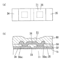
パッケージ133は、図1(a)に示すように、赤外線センサチップ100およびICチップ122が実装されたパッケージ本体134と、パッケージ本体134との間に赤外線センサチップ100およびICチップ122を囲む形でパッケージ本体134に気密的に接合されたパッケージ蓋135とで構成されている。
As shown in FIG. 1A, the package 133 surrounds the infrared sensor chip 100 and the IC chip 122 between the package main body 134 on which the infrared sensor chip 100 and the IC chip 122 are mounted and the package main body 134. The package lid 135 is hermetically bonded to the package body 134.
パッケージ本体134は、ICチップ122と赤外線センサチップ100とが横並びで実装されている。一方、パッケージ蓋135は、赤外線センサチップ100での検知対象の赤外線を透過する機能および導電性を有している。
The package body 134 is mounted with the IC chip 122 and the infrared sensor chip 100 side by side. On the other hand, the package lid 135 has a function of transmitting infrared rays to be detected by the infrared sensor chip 100 and conductivity.
パッケージ蓋135は、パッケージ本体134の上記一表面側に覆着されたキャップ152と、キャップ152において赤外線センサチップ100に対応する部位に形成された開口窓152aを閉塞するレンズ153とで構成されている。ここにおいて、レンズ153が、赤外線を透過する機能を有するとともに、赤外線センサチップ100へ赤外線を収束する機能を有している。なお、レンズ153の代わりに、赤外線を透過する平板状の赤外線透過部材を設けてもよい。
The package lid 135 includes a cap 152 that is covered on the one surface side of the package body 134, and a lens 153 that closes an opening window 152a formed in a portion of the cap 152 corresponding to the infrared sensor chip 100. Yes. Here, the lens 153 has a function of transmitting infrared rays and a function of converging infrared rays to the infrared sensor chip 100. Instead of the lens 153, a plate-shaped infrared transmitting member that transmits infrared light may be provided.
本実施形態の赤外線センサモジュールは、パッケージ本体134とパッケージ蓋135とで構成されるパッケージ133の内部空間(気密空間)165を、ドライ窒素雰囲気としてあるが、これに限らず、例えば、真空雰囲気としてもよい。
In the infrared sensor module of the present embodiment, the internal space (airtight space) 165 of the package 133 constituted by the package body 134 and the package lid 135 is a dry nitrogen atmosphere, but is not limited to this, for example, a vacuum atmosphere Also good.
パッケージ本体134は、絶縁材料からなる基体134aに金属材料からなる配線パターン(図示せず)および電磁シールド層144が形成されており、電磁シールド層144により電磁シールド機能を有している。一方、パッケージ蓋135は、レンズ153およびキャップ152それぞれが導電性を有しており、レンズ153がキャップ152に対して導電性材料により接合されている。したがって、パッケージ蓋135は、レンズ153とキャップ152とが電気的に接続されている。そして、パッケージ蓋135は、パッケージ本体134の電磁シールド層144と電気的に接続されている。しかして、本実施形態では、パッケージ本体134の電磁シールド層144とパッケージ蓋135とを同電位とすることができる。その結果、パッケージ133は、赤外線センサチップ100とICチップ122と上述の配線パターンと後述のボンディングワイヤ(図示せず)と含んで構成されるセンサ回路(図示せず)への外来の電磁ノイズを防止する電磁シールド機能を有している。
In the package body 134, a wiring pattern (not shown) made of a metal material and an electromagnetic shield layer 144 are formed on a base 134a made of an insulating material, and the electromagnetic shield layer 144 has an electromagnetic shield function. On the other hand, in the package lid 135, the lens 153 and the cap 152 each have conductivity, and the lens 153 is bonded to the cap 152 by a conductive material. Therefore, the lens lid 153 and the cap 152 are electrically connected to the package lid 135. The package lid 135 is electrically connected to the electromagnetic shield layer 144 of the package body 134. Therefore, in the present embodiment, the electromagnetic shield layer 144 of the package body 134 and the package lid 135 can be set to the same potential. As a result, the package 133 generates external electromagnetic noise to a sensor circuit (not shown) including the infrared sensor chip 100, the IC chip 122, the above-described wiring pattern, and a bonding wire (not shown) described later. It has an electromagnetic shielding function to prevent.
パッケージ本体134は、赤外線センサチップ100およびICチップ122が一表面側に実装される平板状のセラミック基板により構成してある。要するに、パッケージ本体134は、基体134aが絶縁材料であるセラミックスにより形成されており、上述の配線パターンのうち基体134aの一表面側に形成された部位に、赤外線センサチップ100の各パッドVout1〜Vout8,Vsel1〜Vsel8,Vrefin,Vsu,VzdおよびICチップ122のパッドが、適宜、ボンディングワイヤを介して接続されている。なお、赤外線センサチップ100とICチップ122とは、ボンディングワイヤなどを介して電気的に接続されている。各ボンディングワイヤとしては、Alワイヤに比べて耐腐食性の高いAuワイヤを用いることが好ましい。
The package body 134 is configured by a flat ceramic substrate on which the infrared sensor chip 100 and the IC chip 122 are mounted on one surface side. In short, the package body 134 is formed of ceramics whose base 134a is an insulating material, and each pad Vout1 to Vout8 of the infrared sensor chip 100 is formed on a portion formed on one surface side of the base 134a in the above wiring pattern. , Vsel1 to Vsel8, Vrefin, Vsu, Vzd and the pads of the IC chip 122 are appropriately connected through bonding wires. The infrared sensor chip 100 and the IC chip 122 are electrically connected via a bonding wire or the like. As each bonding wire, it is preferable to use an Au wire having higher corrosion resistance than an Al wire.
本実施形態では、パッケージ本体134の絶縁材料としてセラミックスを採用しているので、上記絶縁材料としてエポキシ樹脂などの有機材料を採用する場合に比べて、パッケージ本体134の耐湿性および耐熱性を向上させることができる。ここで、絶縁材料のセラミックスとして、窒化アルミニウムや炭化珪素などに比べて熱伝導率の小さなアルミナを採用すれば、ICチップ122やパッケージ133の外部からの熱に起因した赤外線センサチップ100の温度上昇を抑制することが可能となる。
In the present embodiment, ceramics is used as the insulating material of the package body 134, so that the moisture resistance and heat resistance of the package body 134 are improved as compared with the case where an organic material such as an epoxy resin is used as the insulating material. be able to. Here, if alumina having a lower thermal conductivity than aluminum nitride or silicon carbide is used as the insulating material ceramic, the temperature of the infrared sensor chip 100 is increased due to heat from the outside of the IC chip 122 and the package 133. Can be suppressed.
また、パッケージ本体134は、上述の配線パターンの一部により構成される外部接続電極(図示せず)が、基体134aの他表面と側面とに跨って形成されている。しかして、本実施形態の赤外線センサモジュールでは、回路基板などへの2次実装後において、回路基板などとの接合部の外観検査を容易に行うことができる。
Further, the package body 134 is formed with external connection electrodes (not shown) constituted by a part of the above-described wiring pattern across the other surface and side surfaces of the base 134a. Therefore, in the infrared sensor module of the present embodiment, after the secondary mounting on the circuit board or the like, it is possible to easily inspect the appearance of the joint portion with the circuit board or the like.
また、赤外線センサチップ100は、パッケージ本体134に対して、第1のダイボンド剤(例えば、シリコーン樹脂など)からなる複数の接合部115を介して実装されている。また、ICチップ122は、パッケージ本体134に対して、第2のダイボンド剤(例えば、シリコーン樹脂など)からなる接合部125を介して実装されている。各ダイボンド剤としては、低融点ガラスやエポキシ系樹脂やシリコーン系樹脂などの絶縁性接着剤、半田(鉛フリー半田、Au−Sn半田など)や銀ペーストなどの導電性接着剤を用いればよい。また、各ダイボンド剤を用いずに、例えば、常温接合法や、Au−Sn共晶もしくはAu−Si共晶を利用した共晶接合法などにより接合してもよい。
The infrared sensor chip 100 is mounted on the package body 134 via a plurality of joints 115 made of a first die bond agent (for example, silicone resin). In addition, the IC chip 122 is mounted on the package body 134 via a bonding portion 125 made of a second die bond agent (for example, silicone resin). As each die bond agent, an insulating adhesive such as low melting glass, epoxy resin, or silicone resin, or conductive adhesive such as solder (lead-free solder, Au—Sn solder, etc.) or silver paste may be used. Further, without using each die-bonding agent, for example, bonding may be performed by a room temperature bonding method or a eutectic bonding method using Au—Sn eutectic or Au—Si eutectic.
上述の赤外線センサモジュールでは、赤外線センサチップ100とパッケージ本体134との間の空間116が断熱部として機能し、しかも、赤外線センサチップ100の裏面の全体をパッケージ本体134に接合する場合に比べて接合部115の断面積を低減できるので、パッケージ本体134から赤外線センサチップ100へ熱が伝達しにくくなる。接合部115には、赤外線センサチップ100とパッケージ本体134との距離を規定するスペーサを混入させてもよく、このようなスペーサを混入させておけば、赤外線センサモジュールの製品間での赤外線センサチップ100とパッケージ本体134との間の熱絶縁性能のばらつきを低減可能となる。
In the infrared sensor module described above, the space 116 between the infrared sensor chip 100 and the package main body 134 functions as a heat insulating portion, and the entire back surface of the infrared sensor chip 100 is bonded to the package main body 134 compared to the case where it is bonded. Since the cross-sectional area of the part 115 can be reduced, it becomes difficult to transfer heat from the package body 134 to the infrared sensor chip 100. A spacer that defines the distance between the infrared sensor chip 100 and the package body 134 may be mixed in the joint 115, and if such a spacer is mixed, the infrared sensor chip between products of the infrared sensor module. The variation in the thermal insulation performance between 100 and the package body 134 can be reduced.
また、ICチップ122は、外周形状が矩形状(正方形状ないし長方形状)であり、裏面全体が接合部125を介してパッケージ本体134に接合されている。
The IC chip 122 has a rectangular outer shape (square shape or rectangular shape), and the entire back surface is bonded to the package body 134 via the bonding portion 125.
パッケージ蓋135は、パッケージ本体134側の一面が開放された箱状に形成され赤外線センサチップ100に対応する部位に開口窓152aが形成されたキャップ152と、キャップ152の開口窓152aを閉塞する形でキャップ152に接合されたレンズ153とで構成されており、キャップ152の上記一面がパッケージ本体134により閉塞される形でパッケージ本体134に気密的に接合されている。ここで、パッケージ本体134の上記一表面の周部には、パッケージ本体134の外周形状に沿った枠状の金属パターン147(図1(a)参照)が全周に亘って形成されている。そして、パッケージ133は、パッケージ蓋135とパッケージ本体134の金属パターン147とが、シーム溶接(抵抗溶接法)により金属接合されているので、気密性および電磁シールド効果を高めることができる。なお、パッケージ蓋135のキャップ152は、コバールにより形成されており、Niめっきが施されている。また、パッケージ本体134の金属パターン147は、コバールにより形成され、Niのめっきが施され、さらにAuのめっきが施されている。
The package lid 135 is formed in a box shape in which one surface on the package body 134 side is opened, and a cap 152 in which an opening window 152a is formed at a portion corresponding to the infrared sensor chip 100, and an opening window 152a of the cap 152 is closed. The lens 153 is joined to the cap 152, and the one surface of the cap 152 is hermetically joined to the package body 134 so as to be closed by the package body 134. Here, a frame-like metal pattern 147 (see FIG. 1A) along the outer peripheral shape of the package main body 134 is formed on the entire periphery of the one surface of the package main body 134. In the package 133, since the package lid 135 and the metal pattern 147 of the package body 134 are metal-bonded by seam welding (resistance welding method), the airtightness and the electromagnetic shielding effect can be enhanced. Note that the cap 152 of the package lid 135 is made of Kovar and plated with Ni. Further, the metal pattern 147 of the package body 134 is formed by Kovar, plated with Ni, and further plated with Au.
パッケージ蓋135とパッケージ本体134の金属パターン147との接合方法は、シーム溶接に限らず、他の溶接(例えば、スポット溶接)や、導電性樹脂により接合してもよい。ここで、導電性樹脂として異方導電性接着剤を用いれば、樹脂(バインダー)中に分散された導電粒子の含有量が少なく、接合時に加熱・加圧を行うことでパッケージ蓋135とパッケージ本体134との接合部の厚みを薄くできるので、外部からパッケージ133内へ水分やガス(例えば、水蒸気、酸素など)が侵入するのを抑制できる。また、導電性樹脂として、酸化バリウム、酸化カルシウムなどの乾燥剤を混入させたものを用いてもよい。
The joining method of the package lid 135 and the metal pattern 147 of the package body 134 is not limited to seam welding, and may be joined by other welding (for example, spot welding) or conductive resin. Here, if an anisotropic conductive adhesive is used as the conductive resin, the content of the conductive particles dispersed in the resin (binder) is small, and the package lid 135 and the package main body are heated and pressed during bonding. Since the thickness of the joint with 134 can be reduced, it is possible to prevent moisture and gas (for example, water vapor, oxygen, etc.) from entering the package 133 from the outside. Further, a conductive resin in which a desiccant such as barium oxide or calcium oxide is mixed may be used.
なお、パッケージ本体134およびパッケージ蓋135の外周形状は矩形状としてあるが、矩形状に限らず、例えば、円形状でもよい。また、パッケージ蓋135のキャップ152は、パッケージ本体134側の端縁から全周に亘って外方に延設された鍔部152bを備えており、鍔部152bが全周に亘ってパッケージ本体134と接合されている。
In addition, although the outer peripheral shape of the package main body 134 and the package lid 135 is a rectangular shape, it is not limited to a rectangular shape, and may be a circular shape, for example. The cap 152 of the package lid 135 includes a flange portion 152b that extends outward from the edge on the package body 134 side over the entire circumference, and the flange portion 152b extends over the entire circumference. It is joined with.
レンズ153は、平凸型の非球面レンズである。しかして、本実施形態の赤外線センサモジュールでは、レンズ153の薄型化を図りながらも、赤外線センサチップ100での赤外線の受光効率の向上による高感度化を図れる。また、本実施形態の赤外線センサモジュールでは、赤外線センサチップ100の検知エリアをレンズ153により設定することが可能となる。レンズ153は、赤外線センサチップ100の半導体基板1とは別の半導体基板(半導体ウェハ)を用いて形成されている。すなわち、レンズ153は、所望のレンズ形状に応じて半導体基板(ここでは、シリコン基板)との接触パターンを設計した陽極を半導体基板の一表面側に半導体基板との接触がオーミック接触となるように形成した後に半導体基板の構成元素の酸化物をエッチング除去する溶液からなる電解液中で半導体基板の他表面側を陽極酸化することで除去部位となる多孔質部を形成してから当該多孔質部を除去することにより形成された半導体レンズ(ここでは、シリコンレンズ)により構成されている。なお、この種の陽極酸化技術を応用した半導体レンズの製造方法については、例えば、特許第3897055号公報、特許第3897056号公報などに開示されている製造方法を適宜に適用することができる。
The lens 153 is a plano-convex aspherical lens. Thus, in the infrared sensor module of the present embodiment, the sensitivity can be increased by improving the infrared light receiving efficiency of the infrared sensor chip 100 while reducing the thickness of the lens 153. In the infrared sensor module of the present embodiment, the detection area of the infrared sensor chip 100 can be set by the lens 153. The lens 153 is formed using a semiconductor substrate (semiconductor wafer) different from the semiconductor substrate 1 of the infrared sensor chip 100. That is, the lens 153 has an anode whose contact pattern is designed with a semiconductor substrate (here, a silicon substrate) according to a desired lens shape so that the contact with the semiconductor substrate becomes ohmic contact with one surface side of the semiconductor substrate. After the formation, the porous portion is formed as a removal site by anodizing the other surface side of the semiconductor substrate in an electrolytic solution composed of a solution for removing the oxide of the constituent element of the semiconductor substrate by etching. It is comprised by the semiconductor lens (here silicon lens) formed by removing. As a method for manufacturing a semiconductor lens to which this kind of anodization technology is applied, for example, a manufacturing method disclosed in Japanese Patent No. 3897055 and Japanese Patent No. 3897056 can be appropriately applied.
本実施形態の赤外線センサモジュールでは、レンズ153として、球面レンズよりも短焦点で且つ開口径が大きく収差が小さな半導体レンズを採用することができるから、短焦点化により、パッケージ133の薄型化を図れる。本実施形態の赤外線センサモジュールは、赤外線センサチップ100の検知対象の赤外線として、人体から放射される10μm付近の波長帯(8μm〜13μm)の赤外線を想定しており、レンズ153の材料として、ZnSやGaAsなどに比べて環境負荷が少なく且つ、Geに比べて低コスト化が可能であり、しかも、ZnSに比べて波長分散が小さなSiを採用している。
In the infrared sensor module according to the present embodiment, a semiconductor lens having a shorter focal point, a larger aperture diameter, and smaller aberration than the spherical lens can be adopted as the lens 153. Therefore, the package 133 can be made thinner by shortening the focal point. . In the infrared sensor module of the present embodiment, an infrared ray having a wavelength band near 10 μm (8 μm to 13 μm) emitted from a human body is assumed as an infrared ray to be detected by the infrared sensor chip 100, and a material of the lens 153 is ZnS. Compared with Ge and GaAs, etc., the environmental load is small, the cost can be reduced as compared with Ge, and Si having a smaller wavelength dispersion than ZnS is adopted.
また、レンズ153は、キャップ152における開口部152aの周部に導電性接着剤(例えば、鉛フリー半田、銀ペーストなど)からなる接合部158により固着されている。上述のように、接合部158の材料として導電性接着剤を採用することにより、レンズ153が、接合部158およびキャップ152を介してパッケージ本体134の電磁シールド層144に電気的に接続されるので、電磁ノイズに対するシールド性を高めることができ、外来の電磁ノイズに起因したS/N比の低下を防止することができる。
The lens 153 is fixed to a peripheral portion of the opening 152a in the cap 152 with a joint 158 made of a conductive adhesive (for example, lead-free solder, silver paste, etc.). As described above, since the lens 153 is electrically connected to the electromagnetic shield layer 144 of the package body 134 via the joint 158 and the cap 152 by using a conductive adhesive as the material of the joint 158. The shielding property against electromagnetic noise can be improved, and the reduction in the S / N ratio due to external electromagnetic noise can be prevented.
上述のレンズ153には、赤外線センサチップ100での検知対象の赤外線の波長を含む所望の波長域の赤外線を透過し当該波長域以外の赤外線を反射する光学多層膜(多層干渉フィルタ膜)からなるフィルタ部(図示せず)を設けることが好ましい。このようなフィルタ部を設けることにより、所望の波長域以外の不要な波長域の赤外線や可視光をフィルタ部によりカットすることが可能となり、太陽光などによるノイズの発生を抑制することができ、高感度化を図れる。
The lens 153 includes an optical multilayer film (multilayer interference filter film) that transmits infrared light in a desired wavelength range including the wavelength of infrared light to be detected by the infrared sensor chip 100 and reflects infrared light outside the wavelength range. It is preferable to provide a filter part (not shown). By providing such a filter part, it becomes possible to cut infrared rays and visible light in an unnecessary wavelength range other than the desired wavelength range by the filter part, and it is possible to suppress the generation of noise due to sunlight, High sensitivity can be achieved.
また、本実施形態では、パッケージ本体134が平板状に形成されているので、パッケージ本体134への赤外線センサチップ100およびICチップ122の実装が容易になるとともに、パッケージ本体134の低コスト化が可能となる。また、パッケージ本体134が平板状に形成されているので、パッケージ本体134を、一面が開放された箱状の形状として、多層セラミック基板により構成し、パッケージ本体134の内底面に赤外線センサチップ100を実装する場合に比べて、パッケージ本体134の上記一表面側に配置される赤外線センサチップ100とレンズ153との間の距離の精度を高めることができ、より一層の高感度化を図れる。なお、以下では、パッケージ本体134において、赤外線センサチップ100を実装する領域を第1の領域140、ICチップ122を実装する領域を第2の領域142と称する。
In this embodiment, since the package body 134 is formed in a flat plate shape, the infrared sensor chip 100 and the IC chip 122 can be easily mounted on the package body 134, and the cost of the package body 134 can be reduced. It becomes. Since the package main body 134 is formed in a flat plate shape, the package main body 134 is formed of a multilayer ceramic substrate in a box shape with one side open, and the infrared sensor chip 100 is formed on the inner bottom surface of the package main body 134. Compared with the case of mounting, the accuracy of the distance between the infrared sensor chip 100 and the lens 153 arranged on the one surface side of the package main body 134 can be improved, and further higher sensitivity can be achieved. In the following description, in the package body 134, an area for mounting the infrared sensor chip 100 is referred to as a first area 140, and an area for mounting the IC chip 122 is referred to as a second area 142.
本実施形態の赤外線センサモジュールでは、パッケージ本体134において、第1の領域140に比べて、第2の領域142の厚みを薄くしてある。ここで、パッケージ本体134の第2の領域142は、基体134aの上記一表面に凹部134bを設けることにより、第1の領域140よりも厚みを薄くしてある。また、パッケージ本体134の第2の領域142では、電磁シールド層144が露出している。
In the infrared sensor module of the present embodiment, the thickness of the second region 142 is made thinner in the package body 134 than in the first region 140. Here, the second region 142 of the package body 134 is made thinner than the first region 140 by providing a recess 134b on the one surface of the base body 134a. Further, the electromagnetic shield layer 144 is exposed in the second region 142 of the package body 134.
また、パッケージ本体134の第2の領域142では、金属材料(例えば、Cuなど)からなる複数のビア(サーマルビア)145が基体134aの厚み方向に貫設されており、各ビア145が電磁シールド層144と接して熱結合されている。
Further, in the second region 142 of the package body 134, a plurality of vias (thermal vias) 145 made of a metal material (for example, Cu) are provided in the thickness direction of the base body 134a, and each via 145 is an electromagnetic shield. It is thermally bonded in contact with layer 144.
ここで、ICチップ122は、第2の領域142において電磁シールド層144に接合部125を介して実装されている。しかして、ICチップ122で発生した熱を電磁シールド層144におけるICチップ122の直下の部位およびビア145を通してパッケージ133の外側へ効率良く放熱させることが可能となる。本実施形態では、電磁シールド層144のうち第2の領域142に形成された部位が、ICチップ122が実装され熱結合される金属部を構成し、各ビア145が、第1の領域140を避けて形成されてパッケージ133の外側に一部が露出する放熱部を構成している。要するに、金属部は、第1の領域140を避けて形成されてパッケージ133の外側に一部が露出する放熱部と熱結合されている。
Here, the IC chip 122 is mounted on the electromagnetic shield layer 144 via the bonding portion 125 in the second region 142. Therefore, it is possible to efficiently dissipate heat generated in the IC chip 122 to the outside of the package 133 through a portion of the electromagnetic shield layer 144 immediately below the IC chip 122 and the via 145. In the present embodiment, a portion of the electromagnetic shield layer 144 formed in the second region 142 constitutes a metal part on which the IC chip 122 is mounted and thermally coupled, and each via 145 defines the first region 140. A heat dissipating part that is formed so as to be partly exposed outside the package 133 is formed. In short, the metal part is formed so as to avoid the first region 140 and is thermally coupled to a heat radiating part that is partially exposed to the outside of the package 133.
次に、本実施形態における赤外線センサチップ100についてさらに詳細に説明する。
Next, the infrared sensor chip 100 in the present embodiment will be described in more detail.
赤外線センサチップ100は、感温部30が埋設された熱型赤外線検出部3とMOSトランジスタ4とを有する複数(a×b個)の画素部2が、半導体基板1の上記一表面側においてアレイ状(ここでは、2次元アレイ状)に配置されている。ここで、半導体基板1の上記一表面は、Si(100)面としてある。感温部30は、複数個(ここでは、6個)のサーモパイル30a(図2参照)を直列接続することにより構成されている。
In the infrared sensor chip 100, a plurality (a × b) of pixel units 2 each having a thermal infrared detection unit 3 in which a temperature sensing unit 30 is embedded and a MOS transistor 4 are arrayed on the one surface side of the semiconductor substrate 1. (In this case, a two-dimensional array). Here, the one surface of the semiconductor substrate 1 is a Si (100) plane. The temperature sensing unit 30 is configured by connecting a plurality of (here, six) thermopiles 30a (see FIG. 2) in series.
各画素部2の熱型赤外線検出部3は、半導体基板1の上記一表面側において熱型赤外線検出部3の形成用領域A1(図4参照)に形成されている。また、各画素部2のMOSトランジスタ4は、半導体基板1の上記一表面側においてMOSトランジスタ4の形成用領域A2(図4参照)に形成されている。
The thermal infrared detector 3 of each pixel unit 2 is formed in the formation area A1 (see FIG. 4) of the thermal infrared detector 3 on the one surface side of the semiconductor substrate 1. Further, the MOS transistor 4 of each pixel portion 2 is formed in the formation region A2 of the MOS transistor 4 (see FIG. 4) on the one surface side of the semiconductor substrate 1.
赤外線センサチップ100は、半導体基板1の上記一表面側において熱型赤外線検出部3の一部の直下に空洞部11が形成されている。熱型赤外線検出部3は、半導体基板1の上記一表面側で空洞部11の周部に形成された支持部3dと、半導体基板1の上記一表面側で平面視において空洞部11を覆う第1の薄膜構造部3aとを備えている。第1の薄膜構造部3aは、赤外線を吸収する赤外線吸収部33を備えている。ここで、第1の薄膜構造部3aは、空洞部11の周方向に沿って並設され支持部3dに支持された複数の第2の薄膜構造部3aaと、隣接する第2の薄膜構造部3aa同士を連結する連結片3c(図2参照)とを有している。なお、図2の例の熱型赤外線検出部3では、複数の線状のスリット13を設けることにより、第1の薄膜構造部3aが6つの第2の薄膜構造部3aaに分離されている。以下では、赤外線吸収部33(第1の赤外線吸収部33と称する)のうち第2の薄膜構造部3aaそれぞれに対応して分割された各部位を第2の赤外線吸収部33aと称する。
In the infrared sensor chip 100, a cavity 11 is formed immediately below a part of the thermal infrared detector 3 on the one surface side of the semiconductor substrate 1. The thermal infrared detector 3 includes a support 3d formed on the periphery of the cavity 11 on the one surface side of the semiconductor substrate 1, and a first cover that covers the cavity 11 in plan view on the one surface side of the semiconductor substrate 1. 1 thin film structure portion 3a. The first thin film structure portion 3a includes an infrared absorbing portion 33 that absorbs infrared rays. Here, the first thin film structure portion 3a includes a plurality of second thin film structure portions 3aa arranged in parallel along the circumferential direction of the cavity portion 11 and supported by the support portion 3d, and adjacent second thin film structure portions. It has the connection piece 3c (refer FIG. 2) which connects 3aa. 2, the first thin film structure portion 3a is separated into six second thin film structure portions 3aa by providing a plurality of linear slits 13. Below, each part divided | segmented corresponding to each 2nd thin film structure part 3aa among the infrared absorption parts 33 (it calls 1st infrared absorption part 33) is called 2nd infrared absorption part 33a.
熱型赤外線検出部3は、第2の薄膜構造部3aaごとにサーモパイル30aが設けられている。ここで、サーモパイル30aは、温接点T1が、第2の薄膜構造部3aaに設けられ、冷接点T2が、支持部3dに設けられている。要するに、温接点T1は、熱型赤外線検出部3において空洞部11に重なる領域に形成され、冷接点T2は、熱型赤外線検出部3において空洞部11に重ならない領域に形成されている。
The thermal infrared detector 3 is provided with a thermopile 30a for each second thin film structure 3aa. Here, in the thermopile 30a, the hot junction T1 is provided in the second thin film structure portion 3aa, and the cold junction T2 is provided in the support portion 3d. In short, the hot junction T1 is formed in a region overlapping the cavity 11 in the thermal infrared detector 3, and the cold junction T2 is formed in a region not overlapping the cavity 11 in the thermal infrared detector 3.
また、熱型赤外線検出部3の感温部30は、各サーモパイル30aごとに出力を取り出す場合に比べて温度変化に対する出力変化が大きくなる接続関係で、全てのサーモパイル30aが電気的に接続されている。図2の例では、感温部30は、6個のサーモパイル30aを直列接続してある。ただし、上述の接続関係は、複数個のサーモパイル30aの全てを直列接続する接続関係に限らない。例えば、それぞれ3個のサーモパイル30aの直列回路を並列接続すれば、6個のサーモパイル30aが並列接続されている場合や、各サーモパイル30aごとに出力を取り出す場合に比べて、感度を高めることができる。また、6個のサーモパイル30aの全てが直列接続されている場合に比べて、感温部30の電気抵抗を低くできて熱雑音が低減されるから、S/N比が向上する。
In addition, the temperature sensing unit 30 of the thermal infrared detection unit 3 has a connection relationship in which the output change with respect to the temperature change is larger than when the output is taken out for each thermopile 30a, and all the thermopile 30a are electrically connected. Yes. In the example of FIG. 2, the temperature sensing unit 30 has six thermopiles 30a connected in series. However, the connection relationship described above is not limited to the connection relationship in which all of the plurality of thermopiles 30a are connected in series. For example, if a series circuit of three thermopiles 30a is connected in parallel, the sensitivity can be increased as compared with the case where six thermopiles 30a are connected in parallel or the output is taken out for each thermopile 30a. . In addition, compared to the case where all of the six thermopiles 30a are connected in series, the electrical resistance of the temperature sensing unit 30 can be lowered and the thermal noise is reduced, so the S / N ratio is improved.
ここで、熱型赤外線検出部3では、第2の薄膜構造部3aaごとに、支持部3dと第2の赤外線吸収部33aとを連結する2つの平面視短冊状のブリッジ部3bb,3bbが空洞部11の周方向に離間して形成されている。これにより、2つのブリッジ部3bb,3bbと第2の赤外線吸収部33aとを空間的に分離し空洞部11に連通する平面視U字状のスリット14が形成されている。熱型赤外線検出部3のうち、平面視において第1の薄膜構造部3aを囲む部位である支持部3dは、矩形枠状の形状となっている。なお、ブリッジ部3bbは、上述の各スリット13,14により、第2の赤外線吸収部33aおよび支持部3dそれぞれとの連結部位以外の部分が、第2の赤外線吸収部33aおよび支持部3dと空間的に分離されている。ここで、第2の薄膜構造部3aaは、支持部3dからの延長方向の寸法を93μm、この延長方向に直交する幅方向の寸法を75μmとし、各ブリッジ部3bbの幅寸法を23μm、各スリット13,14の幅を5μmに設定してあるが、これらの値は一例であって特に限定するものではない。
Here, in the thermal-type infrared detection unit 3, for each second thin film structure unit 3aa, the two bridge portions 3bb and 3bb having a rectangular shape in plan view connecting the support unit 3d and the second infrared absorption unit 33a are hollow. The portions 11 are formed so as to be separated from each other in the circumferential direction. As a result, a slit 14 having a U-shape in plan view that spatially separates the two bridge portions 3bb, 3bb and the second infrared absorbing portion 33a and communicates with the cavity portion 11 is formed. The support part 3d which is a site | part surrounding the 1st thin film structure part 3a in planar view among the thermal-type infrared detection parts 3 has a rectangular frame shape. Note that the bridge portion 3bb has a space other than the second infrared absorption portion 33a and the support portion 3d, and the space between the second infrared absorption portion 33a and the support portion 3d. Separated. Here, in the second thin film structure portion 3aa, the dimension in the extending direction from the support part 3d is 93 μm, the dimension in the width direction orthogonal to the extending direction is 75 μm, the width dimension of each bridge portion 3bb is 23 μm, and each slit Although the widths 13 and 14 are set to 5 μm, these values are merely examples and are not particularly limited.
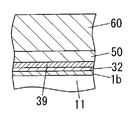
第1の薄膜構造部3aは、半導体基板1の上記一表面側に形成されたシリコン酸化膜1bと、当該シリコン酸化膜1b上に形成されたシリコン窒化膜32と、当該シリコン窒化膜32上に形成された感温部30と、シリコン窒化膜32の表面側で感温部30を覆うように形成された層間絶縁膜50と、層間絶縁膜50上に形成されたパッシベーション膜60との積層構造部をパターニングすることにより形成されている。層間絶縁膜50は、BPSG膜により構成してある。パッシベーション膜60は、PSG膜と当該PSG膜上に形成されたNSG膜との積層膜により構成してあるが、これに限らず、例えば、シリコン窒化膜により構成してもよい。
The first thin film structure portion 3 a includes a silicon oxide film 1 b formed on the one surface side of the semiconductor substrate 1, a silicon nitride film 32 formed on the silicon oxide film 1 b, and the silicon nitride film 32. A laminated structure of the formed temperature sensitive portion 30, an interlayer insulating film 50 formed so as to cover the temperature sensitive portion 30 on the surface side of the silicon nitride film 32, and a passivation film 60 formed on the interlayer insulating film 50. It is formed by patterning the part. The interlayer insulating film 50 is composed of a BPSG film. The passivation film 60 is composed of a laminated film of a PSG film and an NSG film formed on the PSG film, but is not limited thereto, and may be composed of, for example, a silicon nitride film.
上述の熱型赤外線検出部3では、シリコン窒化膜32のうち第1の薄膜構造部3aのブリッジ部3bb,3bb以外の部位が第1の赤外線吸収部33を構成している。また、支持部3dは、シリコン酸化膜1bとシリコン窒化膜32と層間絶縁膜50とパッシベーション膜60とで構成されている。
In the thermal infrared detector 3 described above, portions of the silicon nitride film 32 other than the bridge portions 3bb and 3bb of the first thin film structure portion 3a constitute the first infrared absorber 33. The support 3d is composed of a silicon oxide film 1b, a silicon nitride film 32, an interlayer insulating film 50, and a passivation film 60.
また、赤外線センサチップ100は、層間絶縁膜50とパッシベーション膜60との積層膜が、半導体基板1の上記一表面側において、熱型赤外線検出部3の形成用領域A1とMOSトランジスタ4の形成用領域A2とに跨って形成されており、この積層膜のうち、熱型赤外線検出部3の形成用領域A1に形成された部分が赤外線吸収膜70(図4(b)参照)を兼ねている。ここで、赤外線吸収膜70の屈折率をn2、検出対象の赤外線の中心波長をλとするとき、赤外線吸収膜70の厚さt2をλ/4n2に設定するようにしているので、検出対象の波長(例えば、8〜12μm)の赤外線の吸収効率を高めることができ、高感度化を図れる。例えば、n2=1.4、λ=10μmの場合には、t2≒1.8μmとすればよい。なお、本実施形態では、層間絶縁膜50の膜厚を0.8μm、パッシベーション膜60の膜厚を1μm(PSG膜の膜厚を0.5μm、NSG膜の膜厚を0.5μm)としてある。
Further, in the infrared sensor chip 100, the laminated film of the interlayer insulating film 50 and the passivation film 60 is formed on the one surface side of the semiconductor substrate 1 for forming the formation region A 1 of the thermal infrared detector 3 and the MOS transistor 4. Of the laminated film, the portion formed in the formation region A1 of the thermal infrared detector 3 also serves as the infrared absorption film 70 (see FIG. 4B). . Here, when the refractive index of the infrared absorption film 70 is n 2 and the center wavelength of the infrared ray to be detected is λ, the thickness t2 of the infrared absorption film 70 is set to λ / 4n 2. The absorption efficiency of infrared rays of the target wavelength (for example, 8 to 12 μm) can be increased, and high sensitivity can be achieved. For example, when n 2 = 1.4 and λ = 10 μm, t2≈1.8 μm may be set. In the present embodiment, the interlayer insulating film 50 has a thickness of 0.8 μm, the passivation film 60 has a thickness of 1 μm (the PSG film has a thickness of 0.5 μm, and the NSG film has a thickness of 0.5 μm). .
また、各画素部2では、空洞部11の内周形状が矩形状であり、連結片3cは、平面視X字状に形成されており、第2の薄膜構造部3aaの延長方向に交差する斜め方向において隣接する第2の薄膜構造部3aa,3aa同士、第2の薄膜構造部3aaの延長方向において隣接する第2の薄膜構造部3aa,3aa同士、第2の薄膜構造部3aaの延長方向に直交する方向において隣接する第2の薄膜構造部3aa,3aa同士を連結している。
Further, in each pixel portion 2, the inner peripheral shape of the cavity portion 11 is rectangular, and the connecting piece 3c is formed in an X shape in plan view, and intersects with the extending direction of the second thin film structure portion 3aa. The second thin film structure portions 3aa and 3aa adjacent in the oblique direction, the second thin film structure portions 3aa and 3aa adjacent in the extension direction of the second thin film structure portion 3aa, and the extension direction of the second thin film structure portion 3aa The second thin film structure portions 3aa and 3aa adjacent to each other in the direction orthogonal to are connected to each other.
サーモパイル30aは、シリコン窒化膜32上で第2の薄膜構造部3aaと支持部3dとに跨って形成されたn形ポリシリコン層34とp形ポリシリコン層35との一端部同士を第2の赤外線吸収部33aの赤外線入射面側で金属材料(例えば、Al−Siなど)からなる接続部36により電気的に接続した複数個(図2に示した例では、9個)の熱電対を有している。また、サーモパイル30aは、半導体基板1の上記一表面側で互いに隣り合う熱電対のn形ポリシリコン層34の他端部とp形ポリシリコン層35の他端部とが金属材料(例えば、Al−Siなど)からなる接続部37により接合され電気的に接続されている。ここで、サーモパイル30aは、n形ポリシリコン層34の上記一端部とp形ポリシリコン層35の上記一端部と接続部36とで温接点T1を構成している。また、n形ポリシリコン層34の上記他端部とp形ポリシリコン層35の上記他端部と接続部37とで冷接点T2を構成している。なお、本実施形態における赤外線センサチップ100では、サーモパイル30aの各n形ポリシリコン層34および各p形ポリシリコン層35それぞれにおいて、上述のブリッジ部3bb,3bbに形成されている部位および半導体基板1の上記一表面側のシリコン窒化膜32上に形成されている部位でも赤外線を吸収することができる。
The thermopile 30a has a second end portion of the n-type polysilicon layer 34 and the p-type polysilicon layer 35 formed on the silicon nitride film 32 across the second thin film structure portion 3aa and the support portion 3d. A plurality of (9 in the example shown in FIG. 2) thermocouples electrically connected by the connecting portion 36 made of a metal material (for example, Al—Si) on the infrared incident surface side of the infrared absorbing portion 33a. is doing. In addition, the thermopile 30a has a metal material (for example, Al Al) with the other end of the n-type polysilicon layer 34 and the other end of the p-type polysilicon layer 35 of the thermocouple adjacent to each other on the one surface side of the semiconductor substrate 1. -Si and the like) are joined and electrically connected. Here, in the thermopile 30a, the one end portion of the n-type polysilicon layer 34, the one end portion of the p-type polysilicon layer 35, and the connection portion 36 constitute a hot junction T1. Further, the other end portion of the n-type polysilicon layer 34, the other end portion of the p-type polysilicon layer 35, and the connecting portion 37 constitute a cold junction T2. In the infrared sensor chip 100 according to the present embodiment, each of the n-type polysilicon layer 34 and the p-type polysilicon layer 35 of the thermopile 30a and the portions formed in the above-described bridge portions 3bb and 3bb and the semiconductor substrate 1 Infrared rays can also be absorbed at a portion formed on the silicon nitride film 32 on the one surface side.
また、赤外線センサチップ100は、空洞部11の形状が、四角錘状であり、平面視における中央部の方が周部に比べて深さ寸法が大きくなっているので、第1の薄膜構造部3aの中央部に温接点T1が集まるように各画素部2におけるサーモパイル30aの平面レイアウトを設計してある。すなわち、図2の上下方向における真ん中の2つの第2の薄膜構造部3aaでは、図2および図5に示すように、3つの第2の薄膜構造部3aaの並設方向に沿って温接点T1を並べて配置してあるのに対し、当該上下方向における上側の2つの第2の薄膜構造部3aaでは、図2および図6に示すように、3つの第2の薄膜構造部3aaの並設方向において真ん中の第2の薄膜構造部3aaに近い側に温接点T1を集中して配置してあり、当該上下方向における下側の2つの第2の薄膜構造部3aaでは、図2に示すように、3つの第2の薄膜構造部3aaの並設方向において真ん中の第2の薄膜構造部3aaに近い側に温接点T1を集中して配置してある。しかして、本実施形態における赤外線センサチップ100では、図2の上下方向における上側、下側の第2の薄膜構造部3aaの複数の温接点T1の配置が、真ん中の第2の薄膜構造部3aaの複数の温接点T1の配置と同じである場合に比べて、温接点T1の温度変化を大きくできるので、感度を向上できる。なお、本実施形態では、空洞部11の最深部の深さを所定深さdp(図4(b)参照)とするとき、所定深さdpを200μmに設定してあるが、この値は一例であり、特に限定するものではない。
Further, in the infrared sensor chip 100, the cavity portion 11 has a quadrangular pyramid shape, and the depth of the central portion in plan view is larger than that of the peripheral portion. The planar layout of the thermopile 30a in each pixel unit 2 is designed so that the hot junction T1 gathers at the center of 3a. That is, in the two second thin film structure portions 3aa in the middle in the vertical direction of FIG. 2, as shown in FIGS. 2 and 5, the hot junction T1 is arranged along the juxtaposed direction of the three second thin film structure portions 3aa. Are arranged side by side, in the upper two second thin film structure portions 3aa in the vertical direction, as shown in FIGS. 2 and 6, the parallel arrangement direction of the three second thin film structure portions 3aa In FIG. 2, the hot junctions T1 are concentrated on the side close to the middle second thin film structure 3aa, and the two lower second thin film structures 3aa in the vertical direction are as shown in FIG. In the direction in which the three second thin film structure portions 3aa are arranged side by side, the hot junctions T1 are concentrated on the side close to the middle second thin film structure portion 3aa. Therefore, in the infrared sensor chip 100 in the present embodiment, the arrangement of the plurality of hot junctions T1 of the upper and lower second thin film structure portions 3aa in the vertical direction of FIG. 2 is the middle second thin film structure portion 3aa. Since the temperature change of the hot junction T1 can be increased as compared with the arrangement of the plurality of hot junctions T1, the sensitivity can be improved. In the present embodiment, when the depth of the deepest portion of the cavity portion 11 is a predetermined depth dp (see FIG. 4B), the predetermined depth dp is set to 200 μm, but this value is an example. There is no particular limitation.
また、第2の薄膜構造部3aaは、シリコン窒化膜32の赤外線入射面側においてサーモパイル30aを形成していない領域に、第2の薄膜構造部3aaの反りを抑制するとともに赤外線を吸収するn形ポリシリコン層からなる赤外線吸収層39が形成されている。また、隣接する第2の薄膜構造部3aa,3aa同士を連結する連結片3cには、当該連結片3cを補強するn形ポリシリコン層からなる補強層39b(図7参照)が設けられている。ここで、補強層39bは、赤外線吸収層39と連続一体に形成されている。しかして、赤外線センサチップ100では、連結片3cが補強層39bにより補強されているので、使用中の外部の温度変化や衝撃に起因して発生する応力による破損を防止でき、また、製造時の破損を低減でき、製造歩留まりの向上を図れる。なお、本実施形態では、図7に示す連結片3cの長さ寸法L1を24μm、幅寸法L2を5μm、補強層39bの幅寸法L3を1μmに設定してあるが、これらの数値は一例であり、特に限定するものではない。ただし、本実施形態のように半導体基板1としてシリコン基板を用いており、補強層39bがn形ポリシリコン層により形成される場合には、空洞部11の形成時に補強層39bがエッチングされるのを防止するために、補強層39bの幅寸法は、連結片3cの幅寸法よりも小さく設定し、平面視において補強層39bの両側縁が連結片3cの両側縁よりも内側に位置する必要がある。
Further, the second thin film structure portion 3aa is an n-type that suppresses the warp of the second thin film structure portion 3aa and absorbs infrared rays in a region where the thermopile 30a is not formed on the infrared incident surface side of the silicon nitride film 32. An infrared absorption layer 39 made of a polysilicon layer is formed. Further, the connecting piece 3c that connects the adjacent second thin film structure portions 3aa and 3aa is provided with a reinforcing layer 39b (see FIG. 7) made of an n-type polysilicon layer that reinforces the connecting piece 3c. . Here, the reinforcing layer 39 b is formed integrally with the infrared absorption layer 39. Therefore, in the infrared sensor chip 100, since the connecting piece 3c is reinforced by the reinforcing layer 39b, it is possible to prevent damage due to stress generated due to an external temperature change or impact during use. Breakage can be reduced and the production yield can be improved. In this embodiment, the length L1 of the connecting piece 3c shown in FIG. 7 is set to 24 μm, the width L2 is set to 5 μm, and the width L3 of the reinforcing layer 39b is set to 1 μm. There is no particular limitation. However, when a silicon substrate is used as the semiconductor substrate 1 as in the present embodiment and the reinforcing layer 39b is formed of an n-type polysilicon layer, the reinforcing layer 39b is etched when the cavity 11 is formed. In order to prevent this, the width dimension of the reinforcing layer 39b must be set smaller than the width dimension of the connecting piece 3c, and both side edges of the reinforcing layer 39b need to be located inside the both side edges of the connecting piece 3c in plan view. is there.
また、赤外線センサチップ100は、図7および図12(b)に示すように、連結片3cの両側縁と第2の薄膜構造部3aaの側縁との間にそれぞれ面取り部3d,3dが形成され、X字状の連結片3cの略直交する側縁間にも面取り部3eが形成されている。しかして、赤外線センサチップ100では、図12(a)に示すように面取り部が形成されていない場合に比べて、連結片3cと第2の薄膜構造部3aaとの連結部位での応力集中を緩和でき、製造時に発生する残留応力を低減できるとともに製造時の破損を低減でき、製造歩留まりの向上を図れる。また、使用中の外部の温度変化や衝撃に起因して発生する応力による破損を防止できる。なお、図7に示した例では、各面取り部3d,3eをR(アール)が3μmのR面取り部としてあるが、R面取り部に限らず、例えば、C面取り部としてもよい。
Further, as shown in FIGS. 7 and 12B, the infrared sensor chip 100 has chamfered portions 3d and 3d formed between both side edges of the connecting piece 3c and side edges of the second thin film structure portion 3aa. A chamfered portion 3e is also formed between the side edges of the X-shaped connecting piece 3c that are substantially orthogonal to each other. Thus, in the infrared sensor chip 100, compared to the case where the chamfered portion is not formed as shown in FIG. 12A, the stress concentration at the connecting portion between the connecting piece 3c and the second thin film structure portion 3aa is reduced. This can alleviate the residual stress generated during the manufacturing process and can reduce the damage during the manufacturing process, thereby improving the manufacturing yield. Further, it is possible to prevent damage due to stress generated due to an external temperature change or impact during use. In the example shown in FIG. 7, each of the chamfered portions 3d and 3e is an R chamfered portion having an R (R) of 3 μm, but is not limited to the R chamfered portion, and may be a C chamfered portion, for example.
また、赤外線センサチップ100は、各熱型赤外線検出部3に、支持部3dと一方のブリッジ部3bbと第2の赤外線吸収部33aと他方のブリッジ部3bbと支持部3dとに跨るように引き回されたn形ポリシリコン層からなる故障診断用配線(故障診断用のヒータ)139を設けて、全ての故障診断用配線139を直列接続してある。しかして、a×b個の故障診断用配線139の直列回路へ通電することで、ブリッジ部3bbの折れなどの破損の有無を検出することができる。
In addition, the infrared sensor chip 100 is connected to each thermal infrared detector 3 so as to straddle the support 3d, one bridge 3bb, the second infrared absorber 33a, the other bridge 3bb, and the support 3d. A fault diagnosis wiring (heat diagnosis heater) 139 made of the rotated n-type polysilicon layer is provided, and all the fault diagnosis wirings 139 are connected in series. Accordingly, it is possible to detect the presence or absence of breakage such as breakage of the bridge portion 3bb by energizing the series circuit of the a × b failure diagnosis wirings 139.
要するに、赤外線センサチップ100は、製造途中での検査時や使用時において、a×b個の故障診断用配線139の直列回路への通電の有無によって、ブリッジ部3bbの折れや故障診断用配線139の断線などを検出することができる。また、赤外線センサチップ100では、上述の検査時や使用時において、a×b個の故障診断用配線139の直列回路へ通電して各感温部30の出力を検出することにより、感温部30の断線の有無や感度のばらつき(感温部30の出力のばらつき)などを検知することが可能となる。ここにおいて、感度のばらつきに関しては、画素部2ごとの感度のばらつきを検知することが可能であり、例えば、第1の薄膜構造部3aの反りや第1の薄膜構造部3aの半導体基板1へのスティッキングなどに起因した感度のばらつきを検知することが可能となる。ここで、本実施形態における赤外線センサチップ100では、平面視において、故障診断用配線139を複数の温接点T1の群の付近において折り返され蛇行した形状としてある。したがって、故障診断用配線139へ通電することにより発生するジュール熱によって、各温接点T1を効率良く温めることができる。上述の故障診断用配線139は、n形ポリシリコン層34およびp形ポリシリコン層35と同一平面上に同一厚さで形成されている。
In short, the infrared sensor chip 100 is configured such that the bridge portion 3bb is broken or the failure diagnosis wiring 139 is changed depending on whether or not the series circuit of the a × b failure diagnosis wirings 139 is energized at the time of inspection or use during manufacture. Disconnection can be detected. Further, in the infrared sensor chip 100, during the above-described inspection and use, the temperature sensing unit 30 detects the output of each temperature sensing unit 30 by energizing the series circuit of the a × b fault diagnosis wirings 139. It is possible to detect the presence / absence of disconnection of 30 and variations in sensitivity (variations in output of the temperature sensing unit 30). Here, regarding the sensitivity variation, it is possible to detect the sensitivity variation for each pixel unit 2. For example, the warp of the first thin film structure unit 3 a or the semiconductor substrate 1 of the first thin film structure unit 3 a. It is possible to detect variations in sensitivity due to sticking or the like. Here, in the infrared sensor chip 100 according to the present embodiment, the failure diagnosis wiring 139 is folded and meandered in the vicinity of the group of the plurality of hot junctions T1 in plan view. Therefore, each hot junction T1 can be efficiently warmed by Joule heat generated by energizing the failure diagnosis wiring 139. The above-described failure diagnosis wiring 139 is formed with the same thickness on the same plane as the n-type polysilicon layer 34 and the p-type polysilicon layer 35.
上述の赤外線吸収層39および故障診断用配線139は、n形ポリシリコン層34と同じn形不純物(例えば、リンなど)を同じ不純物濃度(例えば、1018〜1020cm−3)で含んでおり、n形ポリシリコン層34と同時に形成されている。また、p形ポリシリコン層35のp形不純物として例えばボロンを採用すればよく、不純物濃度を例えば1018〜1020cm−3程度の範囲で適宜設定すればよい。本実施形態では、n形ポリシリコン層34およびp形ポリシリコン層35それぞれの不純物濃度が1018〜1020cm−3であり、熱電対の抵抗値を低減でき、S/N比の向上を図れる。なお、赤外線吸収層39および故障診断用配線139は、n形ポリシリコン層34と同じn形不純物を同じ不純物濃度でドーピングしてあるが、これに限らず、例えば、p形ポリシリコン層35と同じ不純物を同じ不純物濃度でドーピングしてもよい。
The infrared absorption layer 39 and the failure diagnosis wiring 139 described above contain the same n-type impurity (for example, phosphorus) as the n-type polysilicon layer 34 at the same impurity concentration (for example, 10 18 to 10 20 cm −3 ). The n-type polysilicon layer 34 is formed at the same time. Further, for example, boron may be adopted as the p-type impurity of the p-type polysilicon layer 35, and the impurity concentration may be appropriately set within a range of, for example, about 10 18 to 10 20 cm −3 . In the present embodiment, the impurity concentration of each of the n-type polysilicon layer 34 and the p-type polysilicon layer 35 is 10 18 to 10 20 cm −3 , the resistance value of the thermocouple can be reduced, and the S / N ratio can be improved. I can plan. The infrared absorption layer 39 and the failure diagnosis wiring 139 are doped with the same n-type impurity as the n-type polysilicon layer 34 at the same impurity concentration. However, the present invention is not limited to this. For example, the p-type polysilicon layer 35 The same impurity may be doped with the same impurity concentration.
赤外線センサチップ100は、n形ポリシリコン層34、p形ポリシリコン層35、赤外線吸収層39、および故障診断用配線139の屈折率をn1、検出対象の赤外線の中心波長をλとするとき、n形ポリシリコン層34、p形ポリシリコン層35、赤外線吸収層39、および故障診断用配線139それぞれの厚さt1をλ/4n1に設定してある。しかして、本実施形態における赤外線センサチップ100では、検出対象の波長(例えば、8〜12μm)の赤外線の吸収効率を高めることができ、高感度化を図れる。例えば、n1=3.6、λ=10μmの場合には、t1≒0.69μmとすればよい。
In the infrared sensor chip 100, when the refractive index of the n-type polysilicon layer 34, the p-type polysilicon layer 35, the infrared absorption layer 39, and the failure diagnosis wiring 139 is n 1 and the center wavelength of the infrared ray to be detected is λ, , it is set n-type polysilicon layer 34, p-type polysilicon layer 35, the infrared-absorbing layer 39, and the failure diagnosis wirings 139 respectively thicknesses t1 to lambda / 4n 1. Therefore, in the infrared sensor chip 100 in this embodiment, the absorption efficiency of infrared rays having a wavelength to be detected (for example, 8 to 12 μm) can be increased, and high sensitivity can be achieved. For example, when n 1 = 3.6 and λ = 10 μm, t 1 ≈0.69 μm may be set.
また、赤外線センサチップ100は、n形ポリシリコン層34、p形ポリシリコン層35、赤外線吸収層39、および故障診断用配線139それぞれの不純物濃度が1018〜1020cm−3であるので、赤外線の吸収率を高くしつつ赤外線の反射を抑制することができて、感温部30の出力のS/N比を高めることができる。また、本実施形態における赤外線センサチップ100では、赤外線吸収層39および故障診断用配線139をn形ポリシリコン層34と同一工程で形成できるから、低コスト化を図れる。
Further, in the infrared sensor chip 100, the n-type polysilicon layer 34, the p-type polysilicon layer 35, the infrared absorption layer 39, and the fault diagnosis wiring 139 each have an impurity concentration of 10 18 to 10 20 cm −3 . Infrared reflection can be suppressed while increasing the infrared absorption rate, and the S / N ratio of the output of the temperature sensing unit 30 can be increased. Further, in the infrared sensor chip 100 according to the present embodiment, the infrared absorption layer 39 and the failure diagnosis wiring 139 can be formed in the same process as the n-type polysilicon layer 34, so that the cost can be reduced.
ここで、感温部30の接続部36と接続部37とは、半導体基板1の上記一表面側において、層間絶縁膜50によって絶縁分離されている(図8および図9参照)。すなわち、温接点T1側の接続部36は、層間絶縁膜50に形成したコンタクトホール50a1,50a2を通して、両ポリシリコン層34,35の上記各一端部と電気的に接続されている。また、冷接点T2側の接続部37は、層間絶縁膜50に形成されたコンタクトホール50a3,50a4を通して、両ポリシリコン層34,35の上記各他端部と電気的に接続されている。
Here, the connection part 36 and the connection part 37 of the temperature sensing part 30 are insulated and separated by the interlayer insulating film 50 on the one surface side of the semiconductor substrate 1 (see FIGS. 8 and 9). That is, the connecting portion 36 on the warm junction T1 side is electrically connected to the one end portions of the polysilicon layers 34 and 35 through the contact holes 50a 1 and 50a 2 formed in the interlayer insulating film 50. Further, the connecting portion 37 on the cold junction T2 side is electrically connected to the other end portions of the polysilicon layers 34 and 35 through contact holes 50a 3 and 50a 4 formed in the interlayer insulating film 50. .
また、MOSトランジスタ4は、上述のように、半導体基板1の上記一表面側においてMOSトランジスタ4の形成用領域A2に形成されている。
Further, the MOS transistor 4 is formed in the formation region A2 of the MOS transistor 4 on the one surface side of the semiconductor substrate 1 as described above.
MOSトランジスタ4は、図4および図11に示すように、半導体基板1の上記一表面側に第1導電形であるp形(p+)のウェル領域41が形成され、ウェル領域41内に、第2導電形であるn形(n+)のドレイン領域43と第2導電形であるn形(n+)のソース領域44とが離間して形成されている。さらに、ウェル領域41内には、ドレイン領域43とソース領域44とを囲む第1導電形であるp形(p++)のチャネルストッパ領域42が形成されている。
As shown in FIGS. 4 and 11, in the MOS transistor 4, a p-type (p + ) well region 41 that is a first conductivity type is formed on the one surface side of the semiconductor substrate 1. An n-type (n + ) drain region 43 that is the second conductivity type and an n-type (n + ) source region 44 that is the second conductivity type are formed apart from each other. Further, in the well region 41, a p-type (p ++ ) channel stopper region 42 which is a first conductivity type surrounding the drain region 43 and the source region 44 is formed.
ウェル領域41においてドレイン領域43とソース領域44との間に位置する部位の上には、シリコン酸化膜(熱酸化膜)からなるゲート絶縁膜45を介してn形ポリシリコン層からなるゲート電極46が形成されている。
A gate electrode 46 made of an n-type polysilicon layer is disposed on a portion of the well region 41 located between the drain region 43 and the source region 44 via a gate insulating film 45 made of a silicon oxide film (thermal oxide film). Is formed.
また、ドレイン領域43上には、金属材料(例えば、Al−Siなど)からなるドレイン電極47が形成され、ソース領域44上には、金属材料(例えば、Al−Siなど)からなるソース電極48が形成されている。
A drain electrode 47 made of a metal material (for example, Al—Si) is formed on the drain region 43, and a source electrode 48 made of a metal material (for example, Al—Si) is formed on the source region 44. Is formed.
ゲート電極46、ドレイン電極47およびソース電極48は、上述の層間絶縁膜50によって絶縁分離されている。ここで、ドレイン電極47は、層間絶縁膜50に形成したコンタクトホール50dを通してドレイン領域43と電気的に接続され、ソース電極48は、層間絶縁膜50に形成したコンタクトホール50eを通してソース領域44と電気的に接続されている。
The gate electrode 46, the drain electrode 47, and the source electrode 48 are insulated and separated by the interlayer insulating film 50 described above. Here, the drain electrode 47 is electrically connected to the drain region 43 through a contact hole 50 d formed in the interlayer insulating film 50, and the source electrode 48 is electrically connected to the source region 44 through a contact hole 50 e formed in the interlayer insulating film 50. Connected.
赤外線センサチップ100の各画素部2では、MOSトランジスタ4のソース電極48と感温部30の一端とが電気的に接続され、感温部30の他端が第4の配線104に電気的に接続されている。また、各画素部2では、MOSトランジスタ4のドレイン電極47が、第1の配線101と電気的に接続され、ゲート電極46が、n形ポリシリコン配線からなる第2の配線102と電気的に接続されている。また、各画素部2では、MOSトランジスタ4のチャネルストッパ領域42上に、金属材料(例えば、Al−Siなど)からなる電極49が形成されている。しかして、ウェル領域41は、チャネルストッパ領域42および電極49を介して、第3の配線103と電気的に接続されている。なお、電極49は、層間絶縁膜50に形成したコンタクトホール50fを通してチャネルストッパ領域42と電気的に接続されている。
In each pixel unit 2 of the infrared sensor chip 100, the source electrode 48 of the MOS transistor 4 and one end of the temperature sensing unit 30 are electrically connected, and the other end of the temperature sensing unit 30 is electrically connected to the fourth wiring 104. It is connected. In each pixel unit 2, the drain electrode 47 of the MOS transistor 4 is electrically connected to the first wiring 101, and the gate electrode 46 is electrically connected to the second wiring 102 made of n-type polysilicon wiring. It is connected. In each pixel portion 2, an electrode 49 made of a metal material (for example, Al—Si) is formed on the channel stopper region 42 of the MOS transistor 4. Thus, the well region 41 is electrically connected to the third wiring 103 through the channel stopper region 42 and the electrode 49. The electrode 49 is electrically connected to the channel stopper region 42 through a contact hole 50f formed in the interlayer insulating film 50.
また、上述のツェナダイオードZDは、図13に示すように、第1拡散領域81上にアノード電極83が形成され、第2拡散領域82上に2つのカソード電極84a,84bが形成されている。このツェナダイオードZDは、アノード電極83が、第5のパッドVzdと電気的に接続され、一方のカソード電極84aが、1つの第2の配線102を介して当該第2の配線102に接続されたMOSトランジスタ4のゲート電極46と電気的に接続され、他方のカソード電極84bが、当該第2の配線102に接続された第2のパッドVsel1〜Vsel8の1つと電気的に接続されている。
In the above Zener diode ZD, the anode electrode 83 is formed on the first diffusion region 81 and the two cathode electrodes 84a and 84b are formed on the second diffusion region 82, as shown in FIG. In this Zener diode ZD, the anode electrode 83 is electrically connected to the fifth pad Vzd, and one cathode electrode 84a is connected to the second wiring 102 via one second wiring 102. The MOS transistor 4 is electrically connected to the gate electrode 46, and the other cathode electrode 84 b is electrically connected to one of the second pads Vsel 1 to Vsel 8 connected to the second wiring 102.
上述の赤外線センサチップ100によれば、故障診断用配線139へ通電してサーモパイル30aの出力を測定することにより、サーモパイル30aの断線などの故障の有無を判断することが可能となって、信頼性の向上を図れる。しかも、赤外線センサチップ100は、故障診断用配線139が、熱型赤外線検出部3において半導体基板1の空洞部11に重なる領域でサーモパイル30aと重ならないように配置されているので、故障診断用配線139によるサーモパイル30aの温接点T1の熱容量の増大を防止でき、感度および応答速度の向上を図れる。
According to the infrared sensor chip 100 described above, by energizing the failure diagnosis wiring 139 and measuring the output of the thermopile 30a, it is possible to determine the presence or absence of a failure such as disconnection of the thermopile 30a. Can be improved. In addition, the infrared sensor chip 100 is arranged so that the failure diagnosis wiring 139 does not overlap the thermopile 30a in a region where the failure detection wiring 139 overlaps the cavity 11 of the semiconductor substrate 1 in the thermal infrared detection unit 3. The increase in the heat capacity of the hot junction T1 of the thermopile 30a due to 139 can be prevented, and the sensitivity and response speed can be improved.
ここで、赤外線センサチップ100は、使用時において自己診断を行わない通常時において、故障診断用配線139も外部からの赤外線を吸収するので、複数の温接点T1の温度の均一化を図れ、感度の向上を図れる。なお、赤外線センサチップ100では、赤外線吸収層39および補強層39bも外部からの赤外線を吸収するので、複数の温接点T1の温度の均一化を図れ、感度の向上を図れる。また、赤外線センサチップ100の使用時の自己診断は、ICチップ122に設けられた自己診断回路(図示せず)により定期的に行われるが、必ずしも定期的に行う必要はない。
Here, in the infrared sensor chip 100, since the failure diagnosis wiring 139 also absorbs infrared rays from the outside during normal times when self-diagnosis is not performed during use, the temperature of the plurality of hot junctions T1 can be made uniform and the sensitivity can be improved. Can be improved. In the infrared sensor chip 100, since the infrared absorbing layer 39 and the reinforcing layer 39b also absorb infrared rays from the outside, the temperature of the plurality of hot junctions T1 can be made uniform, and the sensitivity can be improved. Further, the self-diagnosis when using the infrared sensor chip 100 is periodically performed by a self-diagnosis circuit (not shown) provided in the IC chip 122, but it is not always necessary to perform it periodically.
また、赤外線センサチップ100は、第1の薄膜構造部3aが、複数の第2の薄膜構造部3aaに分離され、各第2の薄膜構造部3aaごとにサーモパイル30aの温接点T1が設けられるとともに、各サーモパイル30aごとに出力を取り出す場合に比べて温度変化に対する出力変化が大きくなる接続関係で全てのサーモパイル30aが電気的に接続されているので、応答速度および感度の向上を図れる。しかも、赤外線センサチップ100は、全ての第2の薄膜構造部3aaに跨って故障診断用配線139が形成されているので、熱型赤外線検出部3の全てのサーモパイル30aを一括して自己診断することが可能となる。また、赤外線センサチップ100では、隣接する第2の薄膜構造部3aa,3aa同士を連結する連結片3cが形成されていることにより、各第2の薄膜構造部3aaの反りを低減でき、構造安定性の向上を図れ、感度が安定する。
Further, in the infrared sensor chip 100, the first thin film structure 3a is separated into a plurality of second thin film structures 3aa, and a hot contact T1 of the thermopile 30a is provided for each second thin film structure 3aa. Since all the thermopile 30a are electrically connected in a connection relationship in which the output change with respect to the temperature change is larger than when the output is taken out for each thermopile 30a, the response speed and the sensitivity can be improved. Moreover, since the failure diagnosis wiring 139 is formed across all the second thin film structures 3aa, the infrared sensor chip 100 performs self-diagnosis of all the thermopiles 30a of the thermal infrared detection unit 3 at once. It becomes possible. Further, in the infrared sensor chip 100, since the connecting pieces 3c that connect the adjacent second thin film structure portions 3aa and 3aa are formed, the warpage of each second thin film structure portion 3aa can be reduced, and the structural stability can be reduced. Improve the stability and stabilize the sensitivity.
また、赤外線センサチップ100は、n形ポリシリコン層34とp形ポリシリコン層35と赤外線吸収層39と補強層39bと故障診断用配線139とが同一の厚さに設定されているので、第2の薄膜構造部3aaの応力バランスの均一性が向上する。これにより、赤外線センサチップ100は、第2の薄膜構造部3aaの反りを抑制することができ、製品ごとの感度のばらつきや、画素部2ごとの感度のばらつきを低減できる。
In the infrared sensor chip 100, the n-type polysilicon layer 34, the p-type polysilicon layer 35, the infrared absorption layer 39, the reinforcing layer 39b, and the failure diagnosis wiring 139 are set to the same thickness. The uniformity of the stress balance of the second thin film structure portion 3aa is improved. Thereby, the infrared sensor chip 100 can suppress the warp of the second thin film structure portion 3aa, and can reduce variations in sensitivity for each product and variations in sensitivity for each pixel portion 2.
また、赤外線センサチップ100は、故障診断用配線139が、第1の熱電要素であるn形ポリシリコン層34もしくは第2の熱電要素であるp形ポリシリコン層35と同じ材料により形成されているので、故障診断用配線139を第1の熱電要素もしくは第2の熱電要素と同時に形成することが可能となり、製造プロセスの簡略化による低コスト化を図れる。
In the infrared sensor chip 100, the fault diagnosis wiring 139 is formed of the same material as the n-type polysilicon layer 34 that is the first thermoelectric element or the p-type polysilicon layer 35 that is the second thermoelectric element. Therefore, the failure diagnosis wiring 139 can be formed simultaneously with the first thermoelectric element or the second thermoelectric element, and the cost can be reduced by simplifying the manufacturing process.
また、赤外線センサチップ100は、赤外線吸収部33および故障診断用配線139を備えた複数の画素部2が、半導体基板1の上記一表面側で2次元アレイ状に設けられているので、製造時や使用時の自己診断に際して各画素部2それぞれの故障診断用配線139に通電することにより、各画素部2それぞれの感温部30の感度のばらつきを把握することが可能となる。
In addition, since the infrared sensor chip 100 is provided with a plurality of pixel portions 2 including the infrared absorbing portion 33 and the failure diagnosis wiring 139 in a two-dimensional array on the one surface side of the semiconductor substrate 1, In addition, when the self-diagnosis at the time of use is applied to the failure diagnosis wiring 139 of each pixel unit 2, it is possible to grasp the variation in sensitivity of the temperature sensing unit 30 of each pixel unit 2.
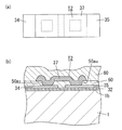
ところで、赤外線センサチップ100は、図1(c)の画素部2の概略平面レイアウト図に示すように、各画素部2ごとにサーモパイル30aの冷接点T2の温度を調整可能な温度調整部90が設けられている。なお、図1(c)は説明を簡単にするために画素部2の構造を簡略化して図示してある。また、温度調整部90は、画素部2における熱型赤外線検出部3の形成用領域A1(図4参照)に形成されている。
By the way, the infrared sensor chip 100 includes a temperature adjustment unit 90 that can adjust the temperature of the cold junction T2 of the thermopile 30a for each pixel unit 2 as shown in the schematic plan layout diagram of the pixel unit 2 in FIG. Is provided. In FIG. 1C, the structure of the pixel portion 2 is simplified for the sake of simplicity. Further, the temperature adjustment unit 90 is formed in the formation region A1 (see FIG. 4) of the thermal infrared detection unit 3 in the pixel unit 2.
図1(c)における温度調整部90は、各画素部2それぞれにおいて冷接点T2における温接点T1側とは反対側に配置された薄膜ヒータ91により構成されており、薄膜ヒータ91の両端部がそれぞれ配線92,92を介して図示しない温度調整部用のパッドと電気的に接続されている。要するに、図1(c)における温度調整部90は、冷接点T2の温度を昇温させる機能を有することで冷接点T2の温度を調整可能である。この温度調整部90は、上述のICチップ122によって制御される。言い換えれば、ICチップ122は、温度調整部90を制御する機能を有している。
The temperature adjusting unit 90 in FIG. 1C is configured by a thin film heater 91 disposed on the opposite side of the cold junction T2 to the warm junction T1 side in each pixel unit 2, and both end portions of the thin film heater 91 are provided. The wirings are electrically connected to pads for temperature adjustment unit (not shown) through wirings 92 and 92, respectively. In short, the temperature adjusting unit 90 in FIG. 1C can adjust the temperature of the cold junction T2 by having a function of raising the temperature of the cold junction T2. The temperature adjustment unit 90 is controlled by the IC chip 122 described above. In other words, the IC chip 122 has a function of controlling the temperature adjustment unit 90.
上述の薄膜ヒータ91は、平面視形状が蛇行した形状に形成されている。また、薄膜ヒータ91は、n形ポリシリコン層により構成してある。ここで、薄膜ヒータ91は、サーモパイル30aのn形ポリシリコン層34およびp形ポリシリコン層35と同一平面上に同一厚さで形成されている。したがって、薄膜ヒータ91をサーモパイル30aのn形ポリシリコン層34と同一工程で形成することが可能となるから、低コスト化を図れる。薄膜ヒータ91は、n形ポリシリコン層に限らず、例えば、p形ポリシリコン層により構成してもよく、この場合は、薄膜ヒータ91をサーモパイル30aのp形ポリシリコン層35と同一工程で形成することが可能となる。なお、薄膜ヒータ91は、金属薄膜により構成してもよい。
The thin film heater 91 described above is formed in a meandering shape in plan view. The thin film heater 91 is composed of an n-type polysilicon layer. Here, the thin film heater 91 is formed with the same thickness on the same plane as the n-type polysilicon layer 34 and the p-type polysilicon layer 35 of the thermopile 30a. Therefore, since the thin film heater 91 can be formed in the same process as the n-type polysilicon layer 34 of the thermopile 30a, the cost can be reduced. The thin film heater 91 is not limited to the n-type polysilicon layer, and may be formed of, for example, a p-type polysilicon layer. In this case, the thin film heater 91 is formed in the same process as the p-type polysilicon layer 35 of the thermopile 30a. It becomes possible to do. The thin film heater 91 may be composed of a metal thin film.
また、赤外線センサチップ100は、各画素部2それぞれにおいて冷接点T2における温接点T1側とは反対側に配置された温度センサ93を備えることが好ましい。この場合、赤外線センサチップ100は、温度センサ93の両端部がそれぞれ配線97,97を介して図示しない温度モニタ用のパッドと電気的に接続されている。これにより、赤外線センサモジュールは、赤外線センサチップ100が温度センサ93によって冷接点T2の温度を検知することができ、ICチップ122が、温度センサ93の出力に基づいて温度調整部90を制御することが可能となる。なお、本実施形態では、温度センサ93よりも温度調整部90を、冷接点T2に近づけて配置してある。
In addition, the infrared sensor chip 100 preferably includes a temperature sensor 93 disposed on the opposite side of the cold junction T2 from the hot junction T1 side in each pixel unit 2. In this case, in the infrared sensor chip 100, both ends of the temperature sensor 93 are electrically connected to a temperature monitoring pad (not shown) via wirings 97 and 97, respectively. Accordingly, in the infrared sensor module, the infrared sensor chip 100 can detect the temperature of the cold junction T2 by the temperature sensor 93, and the IC chip 122 controls the temperature adjustment unit 90 based on the output of the temperature sensor 93. Is possible. In the present embodiment, the temperature adjustment unit 90 is arranged closer to the cold junction T2 than the temperature sensor 93.
温度センサ93は、複数のp形ポリシリコン層94と複数のn形ポリシリコン層95とが金属材料(例えば、Al−Siなど)からなる接続部96により交互に接続されている。ここで、温度センサ93のp形ポリシリコン層94およびn形ポリシリコン層95は、サーモパイル30aのn形ポリシリコン層34およびp形ポリシリコン層35と同一平面上に同一厚さで形成されている。したがって、温度センサ93をサーモパイル30aと同一工程で同時に形成することが可能となるから、低コスト化を図れる。
In the temperature sensor 93, a plurality of p-type polysilicon layers 94 and a plurality of n-type polysilicon layers 95 are alternately connected by connection portions 96 made of a metal material (for example, Al—Si). Here, the p-type polysilicon layer 94 and the n-type polysilicon layer 95 of the temperature sensor 93 are formed with the same thickness on the same plane as the n-type polysilicon layer 34 and the p-type polysilicon layer 35 of the thermopile 30a. Yes. Therefore, the temperature sensor 93 can be simultaneously formed in the same process as the thermopile 30a, so that the cost can be reduced.
以下、赤外線センサチップ100の製造方法の一例について図16〜図19を参照して説明する。
Hereinafter, an example of a method for manufacturing the infrared sensor chip 100 will be described with reference to FIGS.
まず、第2導電形のシリコン基板からなる半導体基板1の上記一表面側に第1の所定膜厚(例えば、0.3μm)の第1のシリコン酸化膜31と第2の所定膜厚(例えば、0.1μm)のシリコン窒化膜32との積層膜からなる絶縁層を形成する絶縁層形成工程を行う。その後、フォトリソグラフィ技術およびエッチング技術を利用して当該絶縁層のうち熱型赤外線検出部3の形成用領域A1に対応する部分の一部を残してMOSトランジスタ4の形成用領域A2に対応する部分をエッチング除去する絶縁層パターニング工程を行うことによって、図16(a)に示す構造を得る。ここにおいて、第1のシリコン酸化膜31は、半導体基板1を所定温度(例えば、1100℃)で熱酸化することにより形成し、シリコン窒化膜32は、LPCVD法により形成している。
First, a first silicon oxide film 31 having a first predetermined film thickness (for example, 0.3 μm) and a second predetermined film thickness (for example, 0.3 μm) are formed on the one surface side of the semiconductor substrate 1 made of a second conductivity type silicon substrate. , 0.1 μm), an insulating layer forming step for forming an insulating layer made of a laminated film with the silicon nitride film 32 is performed. Thereafter, a portion corresponding to the formation region A2 of the MOS transistor 4 is left using the photolithography technique and the etching technique while leaving a part of the insulating layer corresponding to the formation area A1 of the thermal infrared detector 3. The structure shown in FIG. 16A is obtained by performing an insulating layer patterning process for removing the film by etching. Here, the first silicon oxide film 31 is formed by thermally oxidizing the semiconductor substrate 1 at a predetermined temperature (for example, 1100 ° C.), and the silicon nitride film 32 is formed by the LPCVD method.
上述の絶縁層パターニング工程の後、半導体基板1の上記一表面側に第1導電形であるp形(p+)のウェル領域41を形成するウェル領域形成工程を行う。続いて、半導体基板1の上記一表面側におけるウェル領域41内に第1導電形であるp形(p++)のチャネルストッパ領域42を形成するチャネルストッパ領域形成工程を行う。その後、MOSトランジスタ4のしきい値電圧Vthを制御するためのイオン注入工程を行うことによって、図16(b)に示す構造を得る。ここで、ウェル領域形成工程では、まず、半導体基板1の上記一表面側の露出部位を所定温度で熱酸化することにより第2のシリコン酸化膜(熱酸化膜)51を選択的に形成する。その後、ウェル領域41を形成するためのマスクを利用したフォトリソグラフィ技術およびエッチング技術を利用して第2のシリコン酸化膜51をパターニングする。続いて、第1導電形の不純物(ここでは、p形の不純物であり、例えば、ボロンなど)のイオン注入を行ってから、ドライブインを行うことにより、ウェル領域41を形成する。また、チャネルストッパ領域形成工程では、半導体基板1の上記一表面側を所定温度で熱酸化することにより第3のシリコン酸化膜(熱酸化膜)52を選択的に形成する。その後、チャネルストッパ領域42を形成するためのマスクを利用したフォトリソグラフィ技術およびエッチング技術を利用して第3のシリコン酸化膜52をパターニングする。続いて、第1導電形の不純物(ここでは、p形の不純物であり、例えば、ボロンなど)のイオン注入を行ってから、ドライブインを行うことにより、チャネルストッパ領域42を形成する。なお、第1のシリコン酸化膜31と第2のシリコン酸化膜51と第3のシリコン酸化膜52とで、半導体基板1の上記一表面側のシリコン酸化膜1bを構成している。
After the insulating layer patterning step, a well region forming step for forming a p-type (p + ) well region 41 of the first conductivity type on the one surface side of the semiconductor substrate 1 is performed. Subsequently, a channel stopper region forming step of forming a p-type (p ++ ) channel stopper region 42 as the first conductivity type in the well region 41 on the one surface side of the semiconductor substrate 1 is performed. Thereafter, an ion implantation step for controlling the threshold voltage Vth of the MOS transistor 4 is performed to obtain the structure shown in FIG. Here, in the well region forming step, first, the second silicon oxide film (thermal oxide film) 51 is selectively formed by thermally oxidizing the exposed portion on the one surface side of the semiconductor substrate 1 at a predetermined temperature. Thereafter, the second silicon oxide film 51 is patterned using a photolithography technique and an etching technique using a mask for forming the well region 41. Subsequently, the well region 41 is formed by performing ion implantation of a first conductivity type impurity (here, p-type impurity, for example, boron) and then performing drive-in. In the channel stopper region forming step, the third silicon oxide film (thermal oxide film) 52 is selectively formed by thermally oxidizing the one surface side of the semiconductor substrate 1 at a predetermined temperature. Thereafter, the third silicon oxide film 52 is patterned by using a photolithography technique and an etching technique using a mask for forming the channel stopper region 42. Subsequently, the channel stopper region 42 is formed by performing ion implantation of a first conductivity type impurity (here, p-type impurity, for example, boron) and then performing drive-in. Note that the first silicon oxide film 31, the second silicon oxide film 51, and the third silicon oxide film 52 constitute the silicon oxide film 1 b on the one surface side of the semiconductor substrate 1.
上述のイオン注入工程の後、第2導電形であるn形(n+)のドレイン領域43および第2導電形であるn形(n+)のソース領域44を形成するソース・ドレイン形成工程を行う。このソース・ドレイン形成工程では、ウェル領域41におけるドレイン領域43およびソース領域44それぞれの形成予定領域に第2導電形の不純物(ここでは、n形の不純物であり、例えば、リンなど)のイオン注入を行ってから、ドライブを行うことによって、ドレイン領域43およびソース領域44を形成する。
After the above-described ion implantation step, a source / drain formation step of forming an n-type (n + ) drain region 43 that is the second conductivity type and an n-type (n + ) source region 44 that is the second conductivity type is performed. Do. In this source / drain formation step, ions of a second conductivity type impurity (here, an n-type impurity, such as phosphorus) are implanted into the formation region of each of the drain region 43 and the source region 44 in the well region 41. After performing the above, the drain region 43 and the source region 44 are formed by driving.
ソース・ドレイン形成工程の後、半導体基板1の上記一表面側に例えば熱酸化により所定膜厚(例えば、600Å)のシリコン酸化膜(熱酸化膜)からなるゲート絶縁膜45を形成するゲート絶縁膜形成工程を行う。続いて、半導体基板1の上記一表面側の全面にゲート電極46、第2の配線102(図2参照)、n形ポリシリコン層34、p形ポリシリコン層35、薄膜ヒータ91、n形ポリシリコン層95、p形ポリシリコン層94、赤外線吸収層39および故障診断用配線139の基礎となる所定膜厚(例えば、0.69μm)のノンドープポリシリコン層をLPCVD法により形成するポリシリコン層形成工程を行う。その後、フォトリソグラフィ技術およびエッチング技術を利用して上記ノンドープポリシリコン層のうちゲート電極46、第2の配線102、n形ポリシリコン層34、p形ポリシリコン層35、薄膜ヒータ91、n形ポリシリコン層95、p形ポリシリコン層94、赤外線吸収層39および故障診断用配線139それぞれに対応する部分が残るようにパターニングするポリシリコン層パターニング工程を行う。続いて、上記ノンドープポリシリコン層のうちp形ポリシリコン層35およびp形ポリシリコン層94に対応する部分にp形の不純物(例えば、ボロンなど)のイオン注入を行ってからドライブを行うことによりp形ポリシリコン層35およびp形ポリシリコン層94を形成するp形ポリシリコン層形成工程を行う。その後、上記ノンドープポリシリコン層のうちn形ポリシリコン層34、赤外線吸収層39、故障診断用配線139、ゲート電極46および第2の配線102に対応する部分にn形の不純物例えば、リンなど)のイオン注入を行ってからドライブを行うことによりn形ポリシリコン層34、薄膜ヒータ91、n形ポリシリコン層95、赤外線吸収層39、故障診断用配線139、ゲート電極46および第2の配線102を形成するn形ポリシリコン層形成工程を行うことによって、図17(a)に示す構造を得る。なお、p形ポリシリコン層形成工程とn形ポリシリコン層形成工程との順序は逆でもよい。
After the source / drain formation step, a gate insulating film 45 is formed on the one surface side of the semiconductor substrate 1 by, for example, thermal oxidation to form a gate insulating film 45 made of a silicon oxide film (thermal oxide film) having a predetermined thickness (for example, 600 mm). A formation process is performed. Subsequently, the gate electrode 46, the second wiring 102 (see FIG. 2), the n-type polysilicon layer 34, the p-type polysilicon layer 35, the thin film heater 91, and the n-type polysilicon are formed on the entire surface of the semiconductor substrate 1 on the one surface side. Polysilicon layer formation in which a non-doped polysilicon layer having a predetermined film thickness (for example, 0.69 μm) serving as a basis for the silicon layer 95, the p-type polysilicon layer 94, the infrared absorption layer 39, and the failure diagnosis wiring 139 is formed by LPCVD. Perform the process. Thereafter, the gate electrode 46, the second wiring 102, the n-type polysilicon layer 34, the p-type polysilicon layer 35, the thin film heater 91, and the n-type poly-silicon among the non-doped polysilicon layers using the photolithography technique and the etching technique. A polysilicon layer patterning step is performed in which a pattern corresponding to each of the silicon layer 95, the p-type polysilicon layer 94, the infrared absorption layer 39, and the failure diagnosis wiring 139 remains. Subsequently, by performing ion implantation of a p-type impurity (for example, boron) into a portion corresponding to the p-type polysilicon layer 35 and the p-type polysilicon layer 94 in the non-doped polysilicon layer, driving is performed. A p-type polysilicon layer forming step for forming the p-type polysilicon layer 35 and the p-type polysilicon layer 94 is performed. Thereafter, of the non-doped polysilicon layer, the n-type polysilicon layer 34, the infrared absorption layer 39, the failure diagnosis wiring 139, the gate electrode 46, and the portion corresponding to the second wiring 102 are n-type impurities such as phosphorus) The n-type polysilicon layer 34, the thin film heater 91, the n-type polysilicon layer 95, the infrared absorption layer 39, the failure diagnosis wiring 139, the gate electrode 46, and the second wiring 102 are obtained by performing driving after performing ion implantation. The structure shown in FIG. 17A is obtained by performing the n-type polysilicon layer forming step of forming. The order of the p-type polysilicon layer forming step and the n-type polysilicon layer forming step may be reversed.
上述のp形ポリシリコン層形成工程およびn形ポリシリコン層形成工程が終了した後、半導体基板1の上記一表面側に層間絶縁膜50を形成する層間絶縁膜形成工程を行う。続いて、フォトリソグラフィ技術およびエッチング技術を利用して層間絶縁膜50にコンタクトホール50a1,50a2,50a3,50a4,50d,50e,50f(図8、図9、図11参照)を形成するコンタクトホール形成工程を行うことによって、図17(b)に示す構造を得る。層間絶縁膜形成工程では、半導体基板1の上記一表面側に所定膜厚(例えば、0.8μm)のBPSG膜をCVD法により堆積させてから、所定温度(例えば、800℃)でリフローすることにより平坦化された層間絶縁膜50を形成する。また、コンタクトホール形成工程では、薄膜ヒータ91の両端部それぞれの一部を露出させるコンタクトホール(図示せず)や、温度センサ93の接続部96用のコンタクトホール(図示せず)なども形成する。
After the p-type polysilicon layer forming step and the n-type polysilicon layer forming step are completed, an interlayer insulating film forming step for forming an interlayer insulating film 50 on the one surface side of the semiconductor substrate 1 is performed. Subsequently, contact holes 50a 1 , 50a 2 , 50a 3 , 50a 4 , 50d, 50e, 50f (see FIGS. 8, 9, and 11) are formed in the interlayer insulating film 50 using photolithography technology and etching technology. By performing the contact hole forming step, the structure shown in FIG. 17B is obtained. In the interlayer insulating film forming step, a BPSG film having a predetermined film thickness (for example, 0.8 μm) is deposited on the one surface side of the semiconductor substrate 1 by the CVD method, and then reflowed at a predetermined temperature (for example, 800 ° C.). The interlayer insulating film 50 planarized by the above is formed. In the contact hole forming step, a contact hole (not shown) for exposing a part of each end of the thin film heater 91, a contact hole (not shown) for the connection portion 96 of the temperature sensor 93, and the like are also formed. .
上述のコンタクトホール形成工程の後、半導体基板1の上記一表面側の全面に接続部36,37、ドレイン電極47、ソース電極48、第4の配線104、第1の配線101、第3の配線103、パッドVout1〜Vout8,Vsel1〜Vsel8,Vrefin,Vsu(図14参照)、薄膜ヒータ91に接続される配線92、温度センサ93に接続される配線97、上述の温度調整部用のパッド、上述の温度モニタ用のパッドなどの基礎となる所定膜厚(例えば、2μm)の金属膜(例えば、Al−Si膜)を形成する金属膜形成工程を行う。続いて、金属膜をパターニングすることで接続部36,37、ドレイン電極47、ソース電極48、第4の配線104、第1の配線101、第3の配線103、パッドVout1〜Vout8,Vsel1〜Vsel8,Vrefin,Vsuなどを形成する金属膜パターニング工程を行うことによって、図18(a)に示す構造を得る。上述の金属膜形成工程では、金属膜をスパッタ法により形成している。金属膜形成工程での金属膜の形成方法は、スパッタ法に限らず、例えば、CVD法や蒸着法などでもよい。また、金属膜パターニング工程では、フォトリソグラフィ技術およびエッチング技術を利用して金属膜をパターニングする。ここで、金属膜パターニング工程におけるエッチングはRIEにより行っている。なお、この金属膜パターニング工程を行うことにより、温接点T1および冷接点T2が形成される。
After the contact hole forming step, the connection portions 36 and 37, the drain electrode 47, the source electrode 48, the fourth wiring 104, the first wiring 101, and the third wiring are formed on the entire surface of the semiconductor substrate 1 on the one surface side. 103, pads Vout1 to Vout8, Vsel1 to Vsel8, Vrefin, Vsu (see FIG. 14), a wiring 92 connected to the thin film heater 91, a wiring 97 connected to the temperature sensor 93, a pad for the above-described temperature adjustment unit, A metal film forming step of forming a metal film (for example, an Al—Si film) having a predetermined film thickness (for example, 2 μm) serving as a basis for the temperature monitoring pad is performed. Subsequently, by patterning the metal film, the connection portions 36 and 37, the drain electrode 47, the source electrode 48, the fourth wiring 104, the first wiring 101, the third wiring 103, the pads Vout1 to Vout8, Vsel1 to Vsel8. , Vrefin, Vsu, etc. are performed to obtain the structure shown in FIG. In the metal film forming step described above, the metal film is formed by sputtering. The method for forming the metal film in the metal film forming step is not limited to the sputtering method, and for example, a CVD method or a vapor deposition method may be used. In the metal film patterning step, the metal film is patterned using a photolithography technique and an etching technique. Here, etching in the metal film patterning step is performed by RIE. By performing this metal film patterning step, the hot junction T1 and the cold junction T2 are formed.
上述の金属膜パターニング工程の後、半導体基板1の上記一表面側(つまり、層間絶縁膜50の表面側)に所定膜厚(例えば、0.5μm)のPSG膜と所定膜厚(例えば、0.5μm)のNSG膜との積層膜からなるパッシベーション膜60を形成するパッシベーション膜形成工程を行うことによって、図18(b)に示す構造を得る。パッシベーション膜形成工程では、CVD法によってパッシベーション膜60を形成する。
After the metal film patterning step, a PSG film having a predetermined film thickness (for example, 0.5 μm) and a predetermined film thickness (for example, 0 μm) are formed on the one surface side of the semiconductor substrate 1 (that is, the surface side of the interlayer insulating film 50). A passivation film forming step for forming a passivation film 60 made of a laminated film with a (.5 μm) NSG film is performed to obtain the structure shown in FIG. In the passivation film forming step, the passivation film 60 is formed by a CVD method.
上述のパッシベーション膜形成工程の後、第1のシリコン酸化膜31、シリコン窒化膜32、層間絶縁膜50、パッシベーション膜60などを備えた積層構造部をパターニングすることにより、第2の薄膜構造部3aaおよび連結片3cを形成する積層構造部パターニング工程を行うことによって、図19(a)に示す構造を得る。なお、積層構造部パターニング工程を行う際には、既に積層構造部に感温部30などが埋設されている。また、積層構造部パターニング工程において、各スリット13,14を形成している。
After the above-described passivation film forming step, the second thin film structure portion 3aa is patterned by patterning the laminated structure portion including the first silicon oxide film 31, the silicon nitride film 32, the interlayer insulating film 50, the passivation film 60, and the like. And the structure shown to Fig.19 (a) is obtained by performing the laminated structure part patterning process which forms the connection piece 3c. In addition, when performing a laminated structure part patterning process, the temperature sensitive part 30 etc. are already embed | buried in the laminated structure part. Moreover, each slit 13 and 14 is formed in the lamination | stacking structure part patterning process.
上述の積層構造部パターニング工程の後、フォトリソグラフィ技術およびエッチング技術を利用してパッドVout1〜Vout8,Vsel1〜Vsel8,Vrefin,Vsu(図14参照)、上述の温度調整部用のパッド、上述の温度モニタ用のパッドを露出させる開口部(図示せず)を形成する開口部形成工程を行う。次に、各スリット13,14をエッチング液導入孔としてエッチング液を導入し半導体基板1を異方性エッチング(結晶異方性エッチング)することにより半導体基板1に空洞部11を形成する空洞部形成工程を行うことで、図19(b)に示す構造を得る。ここで、開口部形成工程では、フォトリソグラフィ技術およびエッチング技術を利用して上述の開口部を形成する。また、開口部形成工程におけるエッチングはRIEにより行っている。また、空洞部形成工程では、エッチング液として所定温度(例えば、85℃)に加熱したTMAH溶液を用いているが、エッチング液はTMAH溶液に限らず、他のアルカリ系溶液(例えば、KOH溶液など)を用いてもよい。なお、空洞部形成工程が終了するまでの全工程はウェハレベルで行うので、空洞部形成工程が終了した後、個々の赤外線センサチップ100に分離する分離工程を行えばよい。また、上述の製造方法では、ツェナダイオードZDの製造工程について説明を省略したが、イオン注入技術、拡散技術、薄膜形成技術、エッチング技術などを利用して形成することができる。
After the layered structure portion patterning step, the pads Vout1 to Vout8, Vsel1 to Vsel8, Vrefin, Vsu (see FIG. 14), the temperature adjusting portion pad, and the temperature An opening forming step for forming an opening (not shown) for exposing the monitoring pad is performed. Next, the cavity is formed by forming the cavity 11 in the semiconductor substrate 1 by introducing the etchant with the slits 13 and 14 as the etchant introduction holes and anisotropically etching the semiconductor substrate 1 (crystal anisotropic etching). By performing the steps, the structure shown in FIG. 19B is obtained. Here, in the opening forming step, the above-described opening is formed using a photolithography technique and an etching technique. Etching in the opening forming step is performed by RIE. In the cavity forming step, a TMAH solution heated to a predetermined temperature (for example, 85 ° C.) is used as the etching solution. However, the etching solution is not limited to the TMAH solution, and other alkaline solutions (for example, KOH solution, etc.) ) May be used. In addition, since all the processes until the cavity part forming process is completed are performed at the wafer level, a separation process for separating the individual infrared sensor chips 100 may be performed after the cavity part forming process is completed. In the above-described manufacturing method, the description of the manufacturing process of the Zener diode ZD is omitted, but it can be formed using an ion implantation technique, a diffusion technique, a thin film forming technique, an etching technique, and the like.
上述の赤外線センサチップ100では、半導体基板1として上記一表面が(100)面の単結晶シリコン基板を用いて、エッチング速度の結晶面方位依存性を利用した異方性エッチングにより形成する空洞部11を四角錘状の形状としてあるが、四角錘状の形状に限らず、四角錘台状の形状でもよい。また、半導体基板1の上記一表面の面方位は特に限定するものではなく、例えば、半導体基板1として上記一表面がSi(110)面の単結晶のシリコン基板を用いてもよい。また、赤外線センサチップ100において、半導体基板1の空洞部11は、半導体基板1の厚み方向に貫通する形で形成してもよく、この場合は、空洞部11を形成する空洞部形成工程において、半導体基板1の上記一表面とは反対の他表面側から、半導体基板1における空洞部11の形成予定領域を、例えば誘導結合プラズマ(ICP)型のドライエッチング装置を用いた異方性エッチング技術を利用して形成すればよい。また、赤外線センサチップ100は、熱電変換部である感温部30を具備する複数の画素部2が半導体基板1の一表面側においてアレイ状に配置されたものであればよく、構造は特に限定するものではない。また、感温部30を構成するサーモパイル30aの数も複数に限らず、1つでもよい。
In the infrared sensor chip 100 described above, the cavity 11 is formed by anisotropic etching using the dependency of the etching rate on the crystal plane orientation using the single crystal silicon substrate whose one surface is the (100) plane as the semiconductor substrate 1. However, the shape is not limited to the quadrangular pyramid shape, and may be a quadrangular frustum shape. The plane orientation of the one surface of the semiconductor substrate 1 is not particularly limited. For example, a single crystal silicon substrate having the Si (110) surface as the one surface may be used as the semiconductor substrate 1. In the infrared sensor chip 100, the cavity 11 of the semiconductor substrate 1 may be formed so as to penetrate in the thickness direction of the semiconductor substrate 1. In this case, in the cavity forming process for forming the cavity 11, An anisotropic etching technique using, for example, an inductively coupled plasma (ICP) type dry etching apparatus is used to form a cavity 11 formation region in the semiconductor substrate 1 from the other surface side opposite to the one surface of the semiconductor substrate 1. What is necessary is just to form using. The infrared sensor chip 100 may be any structure as long as a plurality of pixel units 2 including the temperature sensing unit 30 that is a thermoelectric conversion unit are arranged in an array on one surface side of the semiconductor substrate 1, and the structure is particularly limited. Not what you want. Moreover, the number of thermopile 30a which comprises the temperature sensing part 30 is not restricted to plural, One may be sufficient.
また、半導体基板1の導電形は、n形に限らず、例えば、図20〜図22に示すようにp形でもよい。図20は、p形の半導体基板1がチャネル形成用領域を構成し、ドレイン領域43およびソース領域44の導電形をn形(n+)とする例である。また、図21は、p形の半導体基板1に形成したp形(p+)のウェル領域41がチャネル形成用領域を構成し、ドレイン領域43およびソース領域44の導電形をn形(n+)とする例である。また、図22は、p形の半導体基板1に形成したn形のウェル領域41がチャネル形成用領域を構成し、ドレイン領域43およびソース領域44の導電形をp形(p+)とする例である。
Further, the conductivity type of the semiconductor substrate 1 is not limited to the n-type, and may be, for example, a p-type as shown in FIGS. FIG. 20 shows an example in which the p-type semiconductor substrate 1 constitutes a channel formation region, and the conductivity type of the drain region 43 and the source region 44 is n-type (n + ). FIG. 21 also shows that a p-type (p + ) well region 41 formed in a p-type semiconductor substrate 1 constitutes a channel formation region, and the conductivity type of the drain region 43 and the source region 44 is n-type (n + ). FIG. 22 shows an example in which the n-type well region 41 formed in the p-type semiconductor substrate 1 constitutes a channel formation region, and the conductivity type of the drain region 43 and the source region 44 is p-type (p + ). It is.
次に、ICチップ122について説明する。
Next, the IC chip 122 will be described.
ICチップ122は、ASIC(:Application Specific IC)であり、シリコン基板を用いて形成されている。また、ICチップ122としてベアチップを用いている。しかして、本実施形態では、ICチップ122がベアチップをパッケージングしたものである場合に比べて、パッケージ133の小型化を図れる。ICチップ122は、赤外線センサチップ100のパッドVout1〜Vout8,Vsel1〜Vsel8,Vrefin,Vsu,Vzd、上述の温度調整部用のパッド、上述の温度モニタ用のパッドそれぞれと適宜に接続される複数のパッド(図示せず)を備えている。
The IC chip 122 is an ASIC (Application Specific IC) and is formed using a silicon substrate. A bare chip is used as the IC chip 122. Therefore, in the present embodiment, the package 133 can be downsized as compared with the case where the IC chip 122 is a package of a bare chip. The IC chip 122 has a plurality of pads Vout1 to Vout8, Vsel1 to Vsel8, Vrefin, Vsu, and Vzd of the infrared sensor chip 100, a pad for the temperature adjusting unit, and a pad for the temperature monitoring as appropriate. A pad (not shown) is provided.
ICチップ122は、赤外線センサチップ100を制御する制御部と、赤外線センサチップ100の出力電圧からなる出力信号を信号処理する信号処理部と、上述の自己診断回路とを備えている。制御部は、赤外線センサチップ100のVsel1〜Vsel8,Vrefin,Vsu,Vzdなどの電位を制御する機能や、温度調整部90を制御する機能などを有している。また、信号処理部は、第1のパッドVout1〜Vout8それぞれに電気的に接続されたパッドの出力電圧(出力信号)を増幅する増幅回路、第1のパッドVout1〜Vout8それぞれに電気的に接続されたパッドの出力電圧を択一的に上記増幅回路に入力するマルチプレクサ、増幅回路の出力をA/D変換するA/D変換回路、A/D変換回路の出力に基づいて適宜の演算を行う演算回路などを備えた回路構成としてあるが、信号処理回路の回路構成は特に限定するものではない。なお、パッケージ133内において、赤外線センサチップ100の近傍に、絶対温度を測定するためのサーミスタを配置して、ICチップ122の演算回路が、上記サーミスタの出力と感温部30の出力とに基づいて温度を演算するようにしてもよい。
The IC chip 122 includes a control unit that controls the infrared sensor chip 100, a signal processing unit that performs signal processing on an output signal that is an output voltage of the infrared sensor chip 100, and the above-described self-diagnosis circuit. The control unit has a function of controlling potentials such as Vsel1 to Vsel8, Vrefin, Vsu, and Vzd of the infrared sensor chip 100, a function of controlling the temperature adjustment unit 90, and the like. In addition, the signal processing unit is electrically connected to each of the first pads Vout1 to Vout8 and an amplifier circuit that amplifies the output voltage (output signal) of the pads electrically connected to each of the first pads Vout1 to Vout8. A multiplexer that alternatively inputs the output voltage of the pad to the amplifier circuit, an A / D converter circuit that performs A / D conversion on the output of the amplifier circuit, and an arithmetic operation that performs appropriate calculations based on the output of the A / D converter circuit Although the circuit configuration includes a circuit and the like, the circuit configuration of the signal processing circuit is not particularly limited. In the package 133, a thermistor for measuring the absolute temperature is arranged in the vicinity of the infrared sensor chip 100, and the arithmetic circuit of the IC chip 122 is based on the output of the thermistor and the output of the temperature sensing unit 30. Thus, the temperature may be calculated.
本実施形態の赤外線センサモジュールの製造にあたっては、パッケージ本体134に赤外線センサチップ100およびICチップ122を実装する実装工程を行ってから、所望の雰囲気中でパッケージ蓋135とパッケージ本体134とを接合する接合工程を行うようにすればよい。
In manufacturing the infrared sensor module of the present embodiment, a mounting process for mounting the infrared sensor chip 100 and the IC chip 122 on the package body 134 is performed, and then the package lid 135 and the package body 134 are joined in a desired atmosphere. What is necessary is just to perform a joining process.
ところで、本実施形態の赤外線センサモジュールにおいて、温度調整部90を設けていない比較例では、レンズ153の形状やパッケージ133内の温度分布の影響で、赤外線センサチップ100における各画素部2の冷接点T2の温度がばらつきやすい。このような温度分布は、例えば、ICチップ122と赤外線センサチップ100との間での熱伝達や、赤外線センサチップ100とパッケージ本体134との間での熱伝達や、赤外線センサチップ100とパッケージ蓋135との間の熱伝達などに起因して生じる。
By the way, in the infrared sensor module of the present embodiment, in the comparative example in which the temperature adjustment unit 90 is not provided, the cold junction of each pixel unit 2 in the infrared sensor chip 100 is affected by the shape of the lens 153 and the temperature distribution in the package 133. The temperature of T2 is likely to vary. Such a temperature distribution may be, for example, heat transfer between the IC chip 122 and the infrared sensor chip 100, heat transfer between the infrared sensor chip 100 and the package body 134, or the infrared sensor chip 100 and the package lid. This is caused by heat transfer to and from 135.
これに対して、本実施形態の赤外線センサモジュールでは、各画素部2ごとにサーモパイル30aの冷接点T2の温度を調整可能な温度調整部90が設けられているので、赤外線センサチップ100の画素部2ごとの感度の均一化を図ることが可能となる。すなわち、本実施形態の赤外線センサモジュールでは、温度調整部90により冷接点T2の温度を調整することにより、赤外線センサチップ100の画素部2ごとの出力を補正することが可能となり、画素部2ごとの感度の均一化を図ることが可能となる。そして、この赤外線センサモジュールにおいては、温度調整部90が、冷接点T2の温度を昇温させる機能を有することで冷接点T2の温度を調整可能であり、ICチップ122が、温度調整部90を制御する機能を有している。ICチップ122において温度調整部90を制御する機能の決定にあたっては、例えば、まず、比較例の赤外線センサモジュールにおいて、赤外線検知エリアを塞ぐ大きさの標準の赤外線源(例えば、黒体、擬似黒体など)からの赤外線を検知させる。ここで、比較例の赤外線センサモジュールの各画素部2の出力が均一化されるように、各冷接点T2の温度の調整度合い(出力の小さな画素部2の出力が増加するように、温度調整部90の制御内容)を決める。そして、この調整度合いに応じたデータを実施形態の赤外線センサモジュールにおけるICチップ122のメモリ(図示せず)などに記憶させておけばよい。なお、温度調整部90の制御内容としては、例えば、各冷接点T2近傍の薄膜ヒータ90への通電量(電流値、電流供給時のオンデューティ)などが挙げられる。
On the other hand, in the infrared sensor module of the present embodiment, since the temperature adjustment unit 90 that can adjust the temperature of the cold junction T2 of the thermopile 30a is provided for each pixel unit 2, the pixel unit of the infrared sensor chip 100 is provided. It becomes possible to make the sensitivity uniform every two. In other words, in the infrared sensor module of the present embodiment, by adjusting the temperature of the cold junction T2 by the temperature adjustment unit 90, the output of each pixel unit 2 of the infrared sensor chip 100 can be corrected. It is possible to make the sensitivity uniform. In this infrared sensor module, the temperature adjustment unit 90 can adjust the temperature of the cold junction T2 by having the function of raising the temperature of the cold junction T2, and the IC chip 122 can adjust the temperature adjustment unit 90. It has a function to control. In determining the function of controlling the temperature adjusting unit 90 in the IC chip 122, for example, in the infrared sensor module of the comparative example, first, a standard infrared source having a size that covers the infrared detection area (for example, a black body or a pseudo black body). Etc.) is detected. Here, the temperature adjustment degree of each cold junction T2 is adjusted so that the output of each pixel unit 2 of the infrared sensor module of the comparative example is uniform (the temperature adjustment is performed so that the output of the pixel unit 2 having a small output increases). Control content of the unit 90). Data corresponding to the degree of adjustment may be stored in a memory (not shown) of the IC chip 122 in the infrared sensor module of the embodiment. The control content of the temperature adjustment unit 90 includes, for example, the energization amount (current value, on-duty when supplying current) to the thin film heater 90 in the vicinity of each cold junction T2.
また、本実施形態の赤外線センサモジュールでは、温度調整部90が、各画素部2それぞれにおいて冷接点T2における温接点T1側とは反対側に配置された薄膜ヒータ91からなるので、赤外線センサチップ100において冷接点T2の近傍に温度調整部90を位置精度良く形成することができ、各画素部2それぞれの冷接点T2を効率良く昇温させることが可能となる。また、ICチップ122において、上述の温度センサ92の出力をモニタしながら温度調整部90を制御するようにすれば、冷接点T2の温度を高精度に制御することが可能となる。この場合、例えば、冷接点T2の温度が最も高い画素部2の冷接点T2の温度と他の画素部2の冷接点T2の温度との差分に基づいて、他の画素部2の温度調整部90を制御するようにすればよい。温度センサ93は、半導体基板1の上記一表面側に設けてあるが、半導体基板1の上記他表面側において、各画素部2それぞれの投影領域内に設けてもよい。
Further, in the infrared sensor module of the present embodiment, the temperature adjustment unit 90 includes the thin film heater 91 disposed on the opposite side of the cold junction T2 to the warm junction T1 side in each pixel unit 2, and thus the infrared sensor chip 100. Therefore, the temperature adjusting unit 90 can be formed with high positional accuracy in the vicinity of the cold junction T2, and the temperature of the cold junction T2 of each pixel unit 2 can be increased efficiently. Further, in the IC chip 122, if the temperature adjustment unit 90 is controlled while monitoring the output of the temperature sensor 92, the temperature of the cold junction T2 can be controlled with high accuracy. In this case, for example, based on the difference between the temperature of the cold junction T2 of the pixel unit 2 having the highest temperature of the cold junction T2 and the temperature of the cold junction T2 of the other pixel unit 2, the temperature adjustment unit of the other pixel unit 2 90 may be controlled. Although the temperature sensor 93 is provided on the one surface side of the semiconductor substrate 1, the temperature sensor 93 may be provided in the projection region of each pixel unit 2 on the other surface side of the semiconductor substrate 1.
また、上述の赤外線センサモジュールは、温度調整部90が、冷接点T2の温度を昇温させることで冷接点T2の温度を調整するものであるが、これに限らず、例えば、温度調整部90が、冷接点T2の温度を降温させる機能を有することで冷接点T2の温度を調整可能であるものとして、ICチップ122が、この温度調整部90を制御する機能を有するようにしてもよい。ここで、比較例の赤外線センサモジュールの各画素部2の出力が均一化されるように、各冷接点T2の温度の調整度合いを決める際には、出力の大きな画素部2の出力が減少するように、ICチップ122による温度調整部90の制御内容を決めればよい。
In the above-described infrared sensor module, the temperature adjustment unit 90 adjusts the temperature of the cold junction T2 by increasing the temperature of the cold junction T2. However, the temperature adjustment unit 90 is not limited thereto. However, the IC chip 122 may have a function of controlling the temperature adjusting unit 90, assuming that the temperature of the cold junction T2 can be adjusted by having the function of lowering the temperature of the cold junction T2. Here, when the degree of adjustment of the temperature of each cold junction T2 is determined so that the output of each pixel unit 2 of the infrared sensor module of the comparative example is made uniform, the output of the pixel unit 2 having a large output decreases. As described above, the control content of the temperature adjustment unit 90 by the IC chip 122 may be determined.
この場合、例えば、図23に示すように、半導体基板1の他表面側において各画素部2それぞれに対応する領域ごとに1対1で配置された複数のペルチェ素子200により温度調整部90を構成してもよい。ここにおいて、各ペルチェ素子200は、例えば、パッケージ本体134に設ければよい。
In this case, for example, as shown in FIG. 23, the temperature adjustment unit 90 is configured by a plurality of Peltier elements 200 arranged in a one-to-one manner for each region corresponding to each pixel unit 2 on the other surface side of the semiconductor substrate 1. May be. Here, each Peltier element 200 may be provided in the package body 134, for example.
また、上述の赤外線センサモジュールは、温度調整部90が冷接点T2の温度を調整するものであるが、これに限らず、温度調整部90が、温接点T1の温度を調整するものでもよい。この場合には、例えば、温度調整部90として、例えば、温接点T1の近傍に薄膜ヒータを配置し、上述の比較例において出力の小さな画素部2の出力が増加するように、ICチップ122による温度調整部90の制御内容を決めればよい。
In the infrared sensor module described above, the temperature adjustment unit 90 adjusts the temperature of the cold junction T2, but the temperature adjustment unit 90 is not limited to this, and the temperature adjustment unit 90 may adjust the temperature of the hot junction T1. In this case, for example, as the temperature adjustment unit 90, for example, a thin film heater is disposed in the vicinity of the hot junction T1, and the IC chip 122 is used so that the output of the pixel unit 2 having a small output increases in the above-described comparative example. What is necessary is just to determine the control content of the temperature adjustment unit 90.
また、赤外線センサモジュールは、温度調整部90が、冷接点T2の温度を昇温させる機能および降温させる機能を有することで冷接点T2の温度を調整可能であり、ICチップ122が、この温度調整部90を制御する機能を有するようにしてもよく、これにより、各冷接点T2の温度の制御性を向上させることが可能となる。この場合、例えば、温度調整部90として、上述の薄膜ヒータ91とペルチェ素子200とを各画素部2ごとに設ければよい。
In addition, the infrared sensor module can adjust the temperature of the cold junction T2 by the temperature adjustment unit 90 having the function of raising and lowering the temperature of the cold junction T2, and the IC chip 122 can adjust the temperature. The function of controlling the unit 90 may be provided, and thereby, the controllability of the temperature of each cold junction T2 can be improved. In this case, for example, the thin film heater 91 and the Peltier element 200 described above may be provided for each pixel unit 2 as the temperature adjustment unit 90.