JP2012153548A - Silicon single-crystal wafer production method and annealed wafer - Google Patents
Silicon single-crystal wafer production method and annealed wafer Download PDFInfo
- Publication number
- JP2012153548A JP2012153548A JP2011011790A JP2011011790A JP2012153548A JP 2012153548 A JP2012153548 A JP 2012153548A JP 2011011790 A JP2011011790 A JP 2011011790A JP 2011011790 A JP2011011790 A JP 2011011790A JP 2012153548 A JP2012153548 A JP 2012153548A
- Authority
- JP
- Japan
- Prior art keywords
- wafer
- silicon single
- single crystal
- less
- region
- Prior art date
- Legal status (The legal status is an assumption and is not a legal conclusion. Google has not performed a legal analysis and makes no representation as to the accuracy of the status listed.)
- Granted
Links
- 239000013078 crystal Substances 0.000 title claims abstract description 67
- XUIMIQQOPSSXEZ-UHFFFAOYSA-N Silicon Chemical compound [Si] XUIMIQQOPSSXEZ-UHFFFAOYSA-N 0.000 title claims abstract description 54
- 229910052710 silicon Inorganic materials 0.000 title claims abstract description 54
- 239000010703 silicon Substances 0.000 title claims abstract description 54
- 238000004519 manufacturing process Methods 0.000 title claims abstract description 20
- 230000007547 defect Effects 0.000 claims abstract description 56
- IJGRMHOSHXDMSA-UHFFFAOYSA-N Atomic nitrogen Chemical compound N#N IJGRMHOSHXDMSA-UHFFFAOYSA-N 0.000 claims abstract description 48
- 238000010438 heat treatment Methods 0.000 claims abstract description 32
- 229910052760 oxygen Inorganic materials 0.000 claims abstract description 28
- 239000001301 oxygen Substances 0.000 claims abstract description 28
- QVGXLLKOCUKJST-UHFFFAOYSA-N atomic oxygen Chemical compound [O] QVGXLLKOCUKJST-UHFFFAOYSA-N 0.000 claims abstract description 27
- 238000000034 method Methods 0.000 claims abstract description 27
- 229910052757 nitrogen Inorganic materials 0.000 claims abstract description 24
- 235000012431 wafers Nutrition 0.000 claims description 102
- 230000007935 neutral effect Effects 0.000 claims description 2
- 238000005121 nitriding Methods 0.000 abstract description 6
- 238000009826 distribution Methods 0.000 abstract description 5
- 230000000052 comparative effect Effects 0.000 description 7
- 239000002019 doping agent Substances 0.000 description 6
- 238000011156 evaluation Methods 0.000 description 6
- 238000009792 diffusion process Methods 0.000 description 4
- 239000002344 surface layer Substances 0.000 description 4
- 230000008034 disappearance Effects 0.000 description 2
- 239000002244 precipitate Substances 0.000 description 2
- 229910052787 antimony Inorganic materials 0.000 description 1
- 229910052785 arsenic Inorganic materials 0.000 description 1
- 230000003247 decreasing effect Effects 0.000 description 1
- 230000007812 deficiency Effects 0.000 description 1
- 230000000694 effects Effects 0.000 description 1
- 229910052751 metal Inorganic materials 0.000 description 1
- 239000002184 metal Substances 0.000 description 1
- 150000002739 metals Chemical class 0.000 description 1
- 150000004767 nitrides Chemical class 0.000 description 1
- 230000002093 peripheral effect Effects 0.000 description 1
- 229910052698 phosphorus Inorganic materials 0.000 description 1
- 238000005498 polishing Methods 0.000 description 1
- 229920001296 polysiloxane Polymers 0.000 description 1
- 239000000758 substrate Substances 0.000 description 1
- 230000008685 targeting Effects 0.000 description 1
Images

Classifications
-
- C—CHEMISTRY; METALLURGY
- C30—CRYSTAL GROWTH
- C30B—SINGLE-CRYSTAL GROWTH; UNIDIRECTIONAL SOLIDIFICATION OF EUTECTIC MATERIAL OR UNIDIRECTIONAL DEMIXING OF EUTECTOID MATERIAL; REFINING BY ZONE-MELTING OF MATERIAL; PRODUCTION OF A HOMOGENEOUS POLYCRYSTALLINE MATERIAL WITH DEFINED STRUCTURE; SINGLE CRYSTALS OR HOMOGENEOUS POLYCRYSTALLINE MATERIAL WITH DEFINED STRUCTURE; AFTER-TREATMENT OF SINGLE CRYSTALS OR A HOMOGENEOUS POLYCRYSTALLINE MATERIAL WITH DEFINED STRUCTURE; APPARATUS THEREFOR
- C30B33/00—After-treatment of single crystals or homogeneous polycrystalline material with defined structure
- C30B33/02—Heat treatment
-
- C—CHEMISTRY; METALLURGY
- C30—CRYSTAL GROWTH
- C30B—SINGLE-CRYSTAL GROWTH; UNIDIRECTIONAL SOLIDIFICATION OF EUTECTIC MATERIAL OR UNIDIRECTIONAL DEMIXING OF EUTECTOID MATERIAL; REFINING BY ZONE-MELTING OF MATERIAL; PRODUCTION OF A HOMOGENEOUS POLYCRYSTALLINE MATERIAL WITH DEFINED STRUCTURE; SINGLE CRYSTALS OR HOMOGENEOUS POLYCRYSTALLINE MATERIAL WITH DEFINED STRUCTURE; AFTER-TREATMENT OF SINGLE CRYSTALS OR A HOMOGENEOUS POLYCRYSTALLINE MATERIAL WITH DEFINED STRUCTURE; APPARATUS THEREFOR
- C30B29/00—Single crystals or homogeneous polycrystalline material with defined structure characterised by the material or by their shape
- C30B29/02—Elements
- C30B29/06—Silicon
-
- H—ELECTRICITY
- H01—ELECTRIC ELEMENTS
- H01L—SEMICONDUCTOR DEVICES NOT COVERED BY CLASS H10
- H01L21/00—Processes or apparatus adapted for the manufacture or treatment of semiconductor or solid state devices or of parts thereof
- H01L21/02—Manufacture or treatment of semiconductor devices or of parts thereof
- H01L21/04—Manufacture or treatment of semiconductor devices or of parts thereof the devices having at least one potential-jump barrier or surface barrier, e.g. PN junction, depletion layer or carrier concentration layer
- H01L21/18—Manufacture or treatment of semiconductor devices or of parts thereof the devices having at least one potential-jump barrier or surface barrier, e.g. PN junction, depletion layer or carrier concentration layer the devices having semiconductor bodies comprising elements of Group IV of the Periodic System or AIIIBV compounds with or without impurities, e.g. doping materials
- H01L21/30—Treatment of semiconductor bodies using processes or apparatus not provided for in groups H01L21/20 - H01L21/26
- H01L21/324—Thermal treatment for modifying the properties of semiconductor bodies, e.g. annealing, sintering
-
- H—ELECTRICITY
- H01—ELECTRIC ELEMENTS
- H01L—SEMICONDUCTOR DEVICES NOT COVERED BY CLASS H10
- H01L29/00—Semiconductor devices adapted for rectifying, amplifying, oscillating or switching, or capacitors or resistors with at least one potential-jump barrier or surface barrier, e.g. PN junction depletion layer or carrier concentration layer; Details of semiconductor bodies or of electrodes thereof ; Multistep manufacturing processes therefor
- H01L29/02—Semiconductor bodies ; Multistep manufacturing processes therefor
- H01L29/30—Semiconductor bodies ; Multistep manufacturing processes therefor characterised by physical imperfections; having polished or roughened surface
- H01L29/32—Semiconductor bodies ; Multistep manufacturing processes therefor characterised by physical imperfections; having polished or roughened surface the imperfections being within the semiconductor body
Abstract
Description
本発明は、例えばIGBT用のシリコン単結晶ウェーハの製造方法に関する。 The present invention relates to a method for manufacturing a silicon single crystal wafer for IGBT, for example.
IGBT(Insulated Gate Bipolar Transistor)のような縦型シリコンデバイス向けのウェーハとしては、一般にFZ法(Floating Zone Method)により製造された導電型がN型のウェーハが用いられている。IGBTは、ウェーハを縦方向に使うデバイスであるため、ウェーハのバルクの品質に影響される。このため、欠陥の少ないウェーハを得られやすいFZ法が用いられている。 As a wafer for a vertical silicon device such as an IGBT (Insulated Gate Bipolar Transistor), a wafer having an N type conductivity manufactured by an FZ method (Floating Zone Method) is generally used. An IGBT is a device that uses a wafer in the vertical direction, and is therefore affected by the quality of the wafer bulk. For this reason, the FZ method in which a wafer with few defects is easily obtained is used.
しかし、FZ法ではウェーハの大口径化は困難で、大量生産には適さない。このため、CZ法(Czochralski Method)で製造された、欠陥領域がN領域で、窒素ドープ、低酸素濃度のウェーハ(特許文献1)や、N領域、低酸素濃度で、RTA処理されたウェーハ(特許文献2)が提案がされている。 However, it is difficult to increase the wafer diameter by the FZ method, which is not suitable for mass production. For this reason, wafers manufactured by the CZ method (Czochralski Method) with a defect region of N region, nitrogen-doped, low oxygen concentration (Patent Document 1), and wafers of N region, low oxygen concentration and RTA processing Patent Document 2) has been proposed.
なお、CZ法におけるウェーハの欠陥領域は、シリコン単結晶インゴットの引き上げ速度に大きく依存して変化するものである。引き上げ速度が高速な領域ではVacancyと呼ばれる点欠陥である空孔が凝集したボイドと考えられるグローイン欠陥が、結晶径方向のほぼ全域に高密度に存在し、これらの欠陥が存在する領域はV領域と呼ばれている。また、引き上げ速度を遅くしていくと、結晶周辺部に発生していたOSFリングが結晶内部に向かって収縮していき、ついには消滅する。更に引き上げ速度を遅くすると、VacancyやInterstitial Silicon(格子間シリコン)の過不足が少ないN(Neutral)領域が出現する。
このN領域のシリコン単結晶を得るための引き上げ速度の幅は狭く、歩留まりが悪いため、高コストのウェーハとなるが、結晶中に欠陥がほとんど無いためIGBT用のウェーハとして用いられていた。
Note that the defect region of the wafer in the CZ method changes greatly depending on the pulling speed of the silicon single crystal ingot. In the region where the pulling rate is high, the glow-in defects considered as voids, which are point defects called vacancy, are present in high density almost all over the crystal diameter direction, and the region where these defects exist is the V region. is called. Further, as the pulling rate is decreased, the OSF ring generated in the periphery of the crystal contracts toward the inside of the crystal and eventually disappears. Further, when the pulling rate is further reduced, an N (Neutral) region in which excess or deficiency of vacancy or interstitial silicon (interstitial silicon) is small appears.
The width of the pulling speed for obtaining the silicon single crystal in the N region is narrow and the yield is poor, so that the wafer becomes high cost. However, since the crystal has almost no defects, it has been used as a wafer for IGBT.
IGBT用ウェーハに対して、ウェーハ面内及び縦方向で抵抗率のばらつきが大きいと、素子間で抵抗率の差が生じ、破損の原因となってしまう。
このため、IGBT用のウェーハとして、面内抵抗率分布が5%以下のウェーハも提案されている(特許文献3、特許文献4)。
If the variation in resistivity is large in the wafer plane and in the vertical direction with respect to the IGBT wafer, a difference in resistivity occurs between elements, which causes damage.
For this reason, wafers having an in-plane resistivity distribution of 5% or less have also been proposed as IGBT wafers (Patent Documents 3 and 4).
しかし、上記のウェーハは、N領域、低酸素濃度のウェーハに窒素ドープ、RTA処理、中性子照射を行うことにより、バルク中の欠陥を無欠陥とし、面内抵抗率分布を改善するというもので、N領域のウェーハの使用が前提となっていた。従って、コストが高く、歩留まりが悪かった。 However, the above-mentioned wafer is such that a defect in the bulk is made defect-free by performing nitrogen doping, RTA treatment, and neutron irradiation on the N region, low oxygen concentration wafer, and the in-plane resistivity distribution is improved. The premise was the use of wafers in the N region. Therefore, the cost is high and the yield is poor.
本発明は、上記問題点に鑑みてなされたものであって、大口径に対応可能なCZ法で製造したV領域のウェーハを用いて、バルク中の欠陥を無欠陥とし、さらに中性子照射を行わなくても、中性子照射を行った場合と同程度の面内抵抗率分布とすることにより、IGBT向けに適用可能な低コストのシリコン単結晶ウェーハを製造する方法を提供することを目的とする。 The present invention has been made in view of the above-described problems, and uses a V-region wafer manufactured by a CZ method capable of handling a large diameter to make defects in the bulk defect-free and further perform neutron irradiation. Even if it is not, it aims at providing the method of manufacturing the low-cost silicon single crystal wafer applicable for IGBT by setting it as the in-plane resistivity distribution comparable to the case where neutron irradiation is performed.
上記目的を達成するために、本発明は、チョクラルスキー法により育成されたV領域のシリコン単結晶インゴットから得られた酸素濃度7ppma(JEIDA:日本電子工業振興協会による換算係数を使用)未満、窒素濃度1×10¹³〜1×10¹⁴atoms/cm3のシリコン単結晶ウェーハに対して、非窒化性雰囲気下、1150〜1300℃で、1〜120分の熱処理を行うことを特徴とするシリコン単結晶ウェーハの製造方法を提供する。 In order to achieve the above object, the present invention provides an oxygen concentration of less than 7 ppma obtained from a V-region silicon single crystal ingot grown by the Czochralski method (JEIDA: using a conversion factor by the Japan Electronics Industry Promotion Association), A silicon single-crystal wafer having a nitrogen concentration of 1 × 10 13 to 1 × 10 14 atoms / cm 3 is subjected to heat treatment at 1150 to 1300 ° C. for 1 to 120 minutes in a non-nitriding atmosphere. A method for producing a single crystal wafer is provided.
上記のシリコン単結晶ウェーハであれば、V領域のシリコン単結晶を用いても、非窒化性雰囲気下、1150〜1300℃で、1〜120分の熱処理を行うことで、表層のみならず、バルク中の結晶欠陥を効果的に低減することができ、さらに、ウェーハの抵抗率の面内ばらつきも改善することができる。このため、本発明の製造方法では、生産性の良いV領域のシリコン単結晶ウェーハを用い、さらに、中性子照射を行うことなく抵抗率の面内ばらつきも改善して、IGBTに適したウェーハを製造できるため、IGBT用ウェーハ製造の生産性を向上させ、コストを低減できる。 If it is said silicon single crystal wafer, even if it uses the silicon | silicone single crystal of V area | region, by performing heat processing for 1 to 120 minutes at 1150-1300 degreeC by non-nitriding atmosphere, not only a surface layer but bulk It is possible to effectively reduce the crystal defects therein, and to improve the in-plane variation of the resistivity of the wafer. For this reason, in the manufacturing method of the present invention, a silicon single crystal wafer in the V region with good productivity is used, and further, in-plane variation of resistivity is improved without performing neutron irradiation, and a wafer suitable for IGBT is manufactured. Therefore, the productivity of manufacturing the wafer for IGBT can be improved and the cost can be reduced.
このとき、前記熱処理を行うことにより、前記シリコン単結晶ウェーハのバルク中の欠陥サイズ15nm以上の結晶欠陥の密度を2×10⁶/cm3以下とすることが好ましい。
このような結晶欠陥の密度とすることで、IGBT等に適した高品質のウェーハとすることができる。
At this time, it is preferable that the density of crystal defects having a defect size of 15 nm or more in the bulk of the silicon single crystal wafer is 2 × 10 6 / cm 3 or less by performing the heat treatment.
By setting the density of such crystal defects, a high-quality wafer suitable for an IGBT or the like can be obtained.
このとき、前記熱処理を行うことにより、前記シリコン単結晶ウェーハの抵抗率の面内ばらつきを5%以下とすることが好ましい。
このように、本発明の方法であれば、中性子照射を行うことなく、熱処理で抵抗率の面内ばらつきを改善することができ、低コストで高品質のウェーハにすることができる。
At this time, it is preferable that the in-plane variation in resistivity of the silicon single crystal wafer is 5% or less by performing the heat treatment.
Thus, according to the method of the present invention, the in-plane variation of resistivity can be improved by heat treatment without performing neutron irradiation, and a high-quality wafer can be obtained at low cost.
このとき、前記シリコン単結晶ウェーハを、導電型がN型で、IGBT向けデバイスに用いるものとすることが好ましい。
本発明の製造方法であれば、このようなIGBT向けデバイスに用いるウェーハを低コストで生産性良く製造することができる。
At this time, it is preferable that the silicon single crystal wafer has an N conductivity type and is used for an IGBT device.
If it is the manufacturing method of this invention, the wafer used for such a device for IGBT can be manufactured at low cost with high productivity.
また、本発明は、チョクラルスキー法により育成されたV領域のシリコン単結晶インゴットから得られた酸素濃度7ppma未満、窒素濃度1×10¹³〜1×10¹⁴atoms/cm3のシリコン単結晶ウェーハを熱処理して製造されたアニールウェーハであって、該アニールウェーハのバルク中の欠陥サイズ15nm以上の結晶欠陥の密度が2×106/cm3以下であることを特徴とするアニールウェーハを提供する。 The present invention also provides a silicon single crystal wafer having an oxygen concentration of less than 7 ppma and a nitrogen concentration of 1 × 10 13 to 1 × 10 14 atoms / cm 3 obtained from a V region silicon single crystal ingot grown by the Czochralski method. An annealed wafer manufactured by heat-treating the wafer, wherein the density of crystal defects having a defect size of 15 nm or more in the bulk of the annealed wafer is 2 × 10 6 / cm 3 or less. .
このようなアニールウェーハであれば、歩留まり良く育成できるV領域のシリコン単結晶インゴットから得られるため低コストで、バルク中の結晶欠陥が非常に少ないため、IGBT用のウェーハとして好適である。 Such an annealed wafer is suitable as an IGBT wafer because it is obtained from a V-region silicon single crystal ingot that can be grown with a high yield and is low in cost and has very few crystal defects in the bulk.
このとき、前記アニールウェーハの抵抗率の面内ばらつきが、5%以下であることが好ましい。
このようウェーハであれば、デバイスを作製した場合、故障の発生を防止でき、歩留まりが向上するウェーハとなる。
At this time, the in-plane variation in resistivity of the annealed wafer is preferably 5% or less.
With such a wafer, when a device is manufactured, the occurrence of a failure can be prevented and the yield can be improved.
このとき、前記アニールウェーハは、導電型がN型で、IGBT向けデバイスに用いるものであることが好ましい。
このように、本発明のアニールウェーハは、IGBT向けデバイスに用いるのに好適である。
At this time, it is preferable that the annealed wafer has an N conductivity type and is used for an IGBT device.
Thus, the annealed wafer of the present invention is suitable for use in a device for IGBT.
以上のように、本発明によれば、V領域のシリコン単結晶ウェーハを用いて、IGBT向けのアニールウェーハを生産性良く低コストで製造することができる。 As described above, according to the present invention, an annealed wafer for IGBT can be manufactured with good productivity and low cost using a V-region silicon single crystal wafer.
以下、本発明について、実施態様の一例として、詳細に説明するが、本発明はこれに限定されるものではない。 Hereinafter, although this invention is demonstrated in detail as an example of an embodiment, this invention is not limited to this.
まず、本発明のアニールウェーハは、チョクラルスキー法により育成されたV領域のシリコン単結晶インゴットから得られた酸素濃度7ppma未満、窒素濃度1×10¹³〜1×10¹⁴atoms/cm3のシリコン単結晶ウェーハを熱処理して製造されたアニールウェーハであって、該アニールウェーハのバルク中の欠陥サイズ15nm以上の結晶欠陥の密度が2×106/cm3以下である。 First, the annealed wafer of the present invention is silicon having an oxygen concentration of less than 7 ppma and a nitrogen concentration of 1 × 10 13 to 1 × 10 14 atoms / cm 3 obtained from a V-region silicon single crystal ingot grown by the Czochralski method. An annealed wafer manufactured by heat-treating a single crystal wafer, and the density of crystal defects having a defect size of 15 nm or more in the bulk of the annealed wafer is 2 × 10 6 / cm 3 or less.
このようなアニールウェーハであれば、問題となるような大きさの結晶欠陥がバルク中に非常に少ないため、例えばウェーハの縦方向(厚さ方向)に素子が形成されるIGBT向けのウェーハとして好適である。また、V領域のシリコン単結晶インゴットから得られるものであるため生産性良く製造できる。 With such an annealed wafer, there are very few crystal defects of a problem size in the bulk, so it is suitable as a wafer for an IGBT in which elements are formed in the longitudinal direction (thickness direction) of the wafer, for example. It is. Further, since it is obtained from a silicon single crystal ingot in the V region, it can be manufactured with high productivity.
このとき、本発明のアニールウェーハの抵抗率の面内ばらつきが、5%以下であることが好ましい。
このような中性子照射を用いることなく熱処理により抵抗率の均一性が上記範囲にまで向上されたウェーハであれば、高品質で安価なIGBT用ウェーハとすることができる。
At this time, the in-plane variation in resistivity of the annealed wafer of the present invention is preferably 5% or less.
As long as the uniformity of resistivity is improved to the above range by heat treatment without using such neutron irradiation, a high-quality and inexpensive IGBT wafer can be obtained.
このような本発明のアニールウェーハは、導電型がN型であれば、IGBT向けデバイスに用いるウェーハとして好適である。 Such an annealed wafer of the present invention is suitable as a wafer used for an IGBT device if the conductivity type is N-type.
上記のような本発明のアニールウェーハを製造する方法の一例として、本発明のシリコン単結晶ウェーハの製造方法を以下に説明する。 As an example of the method for producing the annealed wafer of the present invention as described above, the method for producing a silicon single crystal wafer of the present invention will be described below.
本発明のシリコン単結晶ウェーハの製造方法では、チョクラルスキー法により育成されたV領域のシリコン単結晶インゴットから得られた酸素濃度7ppma未満、窒素濃度1×10¹³〜1×10¹⁴atoms/cm3のシリコン単結晶ウェーハに対して、非窒化性雰囲気下、1150〜1300℃で、1〜120分の熱処理を行う。 In the method for producing a silicon single crystal wafer of the present invention, an oxygen concentration of less than 7 ppma and a nitrogen concentration of 1 × 10 13 to 1 × 10 14 atoms / cm obtained from a V region silicon single crystal ingot grown by the Czochralski method. 3 is subjected to heat treatment at 1150 to 1300 ° C. for 1 to 120 minutes in a non-nitriding atmosphere.
本発明において、例えば、MCZ法により、欠陥領域がV領域となるように引き上げ速度等を制御しながら、さらに、酸素濃度が7ppma未満となるように、シリコン単結晶インゴットを育成する。この際、窒素濃度1×10¹³〜1×10¹⁴atoms/cm3となるように窒素をドープする。また、例えば導電型をN型とする場合には、ドーパントとして、P、As、Sb等をドープすることもできる。
そして、このように育成したシリコン単結晶インゴットをスライスし、研磨等を行うことで、酸素濃度7ppma未満、窒素濃度1×10¹³〜1×10¹⁴atoms/cm3で、全面がV領域のシリコン単結晶ウェーハを作製することができる。
In the present invention, for example, a silicon single crystal ingot is grown by the MCZ method so that the oxygen concentration is less than 7 ppma while controlling the pulling rate so that the defect region becomes the V region. At this time, nitrogen is doped so that the nitrogen concentration is 1 × 10 13 to 1 × 10 14 atoms / cm 3 . For example, when the conductivity type is N-type, P, As, Sb, or the like can be doped as a dopant.
Then, the silicon single crystal ingot grown in this way is sliced and polished, so that the silicon concentration is less than 7 ppma, the nitrogen concentration is 1 × 10 13 to 1 × 10 14 atoms / cm 3 , and the entire surface is V region silicon. A single crystal wafer can be produced.
このように、従来ではIGBT用にN領域のウェーハを用いていたが、本発明ではV領域のウェーハを用いることができるため、インゴット育成時の引き上げ速度のマージンを拡大でき、ウェーハ製造の生産性が向上する。また、CZ法を用いるので、大口径のウェーハを得るのが容易である。 As described above, the N region wafer is conventionally used for the IGBT. However, since the V region wafer can be used in the present invention, the margin of the pulling speed at the time of ingot growth can be increased, and the productivity of the wafer manufacture Will improve. Moreover, since the CZ method is used, it is easy to obtain a large-diameter wafer.
この際、窒素濃度が1×10¹³atoms/cm3未満では、ウェーハの酸素析出物のサイズが大きくなり、後工程の熱処理によりバルク内部の欠陥の消滅が困難となる。窒素濃度が1×1014atoms/cm3より大きい場合には、ウェーハ外周にOSFが形成される。 At this time, if the nitrogen concentration is less than 1 × 10 13 atoms / cm 3 , the size of oxygen precipitates on the wafer becomes large, and it becomes difficult to eliminate defects inside the bulk by a heat treatment in a later step. When the nitrogen concentration is higher than 1 × 10 14 atoms / cm 3 , OSF is formed on the outer periphery of the wafer.
また、本発明のシリコン単結晶ウェーハの酸素濃度は、7ppma未満、好ましくは5ppma以下であり、このような極低酸素濃度であれば熱処理によりウェーハ中の欠陥を十分に消滅させることができ、一方、酸素濃度が7ppma以上になると、熱処理によって欠陥が消滅しにくくなり、特にバルク中の欠陥が多く残ってしまう。
このように、本発明において、酸素濃度と窒素濃度を上記範囲とすることで、ウェーハ中の酸素析出物サイズが、MO601(三井金属製)により、赤外線の散乱強度で評価すると250a.u以下と小さくなり、その後の熱処理により欠陥を消滅しやすくなる。
Further, the oxygen concentration of the silicon single crystal wafer of the present invention is less than 7 ppma, preferably 5 ppma or less. With such an extremely low oxygen concentration, defects in the wafer can be sufficiently eliminated by heat treatment, When the oxygen concentration is 7 ppma or more, defects are difficult to disappear by heat treatment, and many defects in the bulk remain in particular.
As described above, in the present invention, when the oxygen concentration and the nitrogen concentration are within the above ranges, the size of the oxygen precipitate in the wafer is 250a. It becomes small below u, and it becomes easy to eliminate defects by subsequent heat treatment.
そして、このようなシリコン単結晶ウェーハに対して、例えば縦型熱処理炉で、Ar、H2、Ar+O2等の非窒化性雰囲気下、1150〜1300℃で1〜120分の熱処理を行う。
この熱処理において、表層の酸素が外方拡散し、さらに、バルク中のグローイン欠陥の内壁の酸化膜が溶解し、空洞の縮小、さらには空洞が埋まることによって、バルク中の欠陥サイズ15nm以上の結晶欠陥の密度を2×10⁶/cm3以下とすることができる。
Then, such a silicon single crystal wafer is heat-treated at 1150 to 1300 ° C. for 1 to 120 minutes in a non-nitriding atmosphere such as Ar, H 2 , Ar + O 2 or the like in a vertical heat treatment furnace, for example.
In this heat treatment, oxygen in the surface layer diffuses outward, the oxide film on the inner wall of the glow-in defect in the bulk dissolves, the cavity is reduced, and the cavity is filled, so that a crystal having a defect size of 15 nm or more in the bulk is obtained. The density of defects can be 2 × 10 6 / cm 3 or less.
このときNH3、N2等の窒化性雰囲気下で熱処理を行うと、ウェーハ表面に窒化膜が形成されてしまい、酸素の外方拡散を妨げ、欠陥の消滅が十分にできない。
また、熱処理温度は、1150℃未満では欠陥の消滅が不十分で、1300℃を超えると、スリップ転位が発生することがある。さらに、この熱処理温度は1200℃以下がスリップ転位発生を確実に防止できるため、好ましい。熱処理時間は、1分以上であれば欠陥の消滅を効果的に達成でき、120分以下であれば十分であり、またスリップ転位の発生を抑制できる。
At this time, if heat treatment is performed in a nitriding atmosphere such as NH 3 or N 2 , a nitride film is formed on the wafer surface, preventing oxygen from diffusing outwardly, and defects cannot be sufficiently eliminated.
Further, when the heat treatment temperature is less than 1150 ° C., the disappearance of defects is insufficient, and when it exceeds 1300 ° C., slip dislocation may occur. Further, the heat treatment temperature is preferably 1200 ° C. or lower because slip dislocation can be reliably prevented. If the heat treatment time is 1 minute or longer, the disappearance of defects can be effectively achieved, and if it is 120 minutes or shorter, it is sufficient, and the occurrence of slip dislocation can be suppressed.
この熱処理により、ウェーハの抵抗率の面内ばらつきを5%以下とすることができる。
従来では、このような面内均一な抵抗率を得るためには、中性子照射が必要で、この処理によりコストが高くなっていた。しかし、本発明者らは、以下のような知見から熱処理による抵抗率均一化の方法を見出した。
By this heat treatment, the in-plane variation of the resistivity of the wafer can be reduced to 5% or less.
Conventionally, in order to obtain such an in-plane uniform resistivity, neutron irradiation is required, and this processing has increased the cost. However, the present inventors have found a method of uniforming resistivity by heat treatment from the following knowledge.
P等のドーパントの拡散は、ドーパント単体での拡散ではなく、ドーパントとI(Si)(格子間シリコン)のペアで拡散する。特に、Vacancyが存在する場合、ドーパント+I(Si)の拡散を促進する。
従って、本発明の窒素ドープ+低酸素ウェーハに対して上記の高温熱処理を行うと、窒素の外方拡散が起こり、さらに、酸素が少ないため、過剰なVacancyが発生する。この大量のVacancyの発生により、ドーパント+I(Si)の拡散が促進され、抵抗率が均一方向に変化することを見出した。
このような本発明の熱処理により中性子照射と同等以上の抵抗率均一化が可能で、IGBT用ウェーハの製造コストを効果的に低減することができる。
Diffusion of a dopant such as P is not performed by a single dopant, but by a pair of dopant and I (Si) (interstitial silicon). In particular, when vacancy is present, it facilitates diffusion of dopant + I (Si).
Therefore, when the above-described high-temperature heat treatment is performed on the nitrogen-doped + low-oxygen wafer according to the present invention, out-diffusion of nitrogen occurs, and more oxygen is generated due to less oxygen. It has been found that the generation of this large amount of vacancy promotes the diffusion of dopant + I (Si) and the resistivity changes in a uniform direction.
Such a heat treatment according to the present invention makes it possible to equalize the resistivity equal to or higher than that of neutron irradiation, and effectively reduce the manufacturing cost of the IGBT wafer.
以上のような本発明のシリコン単結晶ウェーハの製造方法であれば、導電型をN型とすることでIGBT向けデバイスに用いるのに好適なウェーハを低コストで生産性良く製造することができる。
ただし、本発明のアニールウェーハ及びシリコン単結晶ウェーハの製造方法で製造したウェーハは、IGBT以外のデバイスにも用いることができる。
With the method for manufacturing a silicon single crystal wafer of the present invention as described above, a wafer suitable for use in a device for IGBT can be manufactured with low cost and high productivity by making the conductivity type N type.
However, the wafer manufactured by the manufacturing method of the annealed wafer and the silicon single crystal wafer of the present invention can be used for devices other than IGBTs.
以下、実施例及び比較例を示して本発明をより具体的に説明するが、本発明はこれらに限定されるものではない。
(実施例1、比較例1)
(酸素濃度の臨界的意義の証明)
チョクラルスキー法により得られた、窒素濃度5×10¹³atoms/cm3でV領域のシリコン単結晶ウェーハを、酸素濃度が4ppma,6ppma,8ppma(JEIDA)の三種類用意して、Ar雰囲気下、1170℃、1時間の熱処理を行った。
EXAMPLES Hereinafter, although an Example and a comparative example are shown and this invention is demonstrated more concretely, this invention is not limited to these.
(Example 1, Comparative Example 1)
(Proof of critical significance of oxygen concentration)
Three types of silicon single crystal wafers obtained by the Czochralski method and having a nitrogen concentration of 5 × 10 13 atoms / cm 3 and a V region with oxygen concentrations of 4 ppma, 6 ppma, and 8 ppma (JEIDA) are prepared in an Ar atmosphere. Heat treatment was performed at 1170 ° C. for 1 hour.
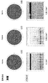
この熱処理したウェーハについて、MO601(三井金属製)を用いて、サイズが15nm以上の結晶欠陥の密度を評価した。MO601は表層5μm付近の欠陥評価が可能である。
評価の際、バルク中の欠陥評価は、深さ方向研磨(50μm、100μm狙い)し、MO601で評価を行った。この評価方法は研磨面の全面評価が可能である。
評価結果を図1,表1に示す。
About this heat-processed wafer, the density of the crystal defect whose size is 15 nm or more was evaluated using MO601 (made by Mitsui Metals). MO601 can evaluate defects near the surface layer of 5 μm.
At the time of evaluation, defects in the bulk were evaluated by MO 601 after polishing in the depth direction (targeting 50 μm and 100 μm). This evaluation method can evaluate the entire polished surface.
The evaluation results are shown in FIG.
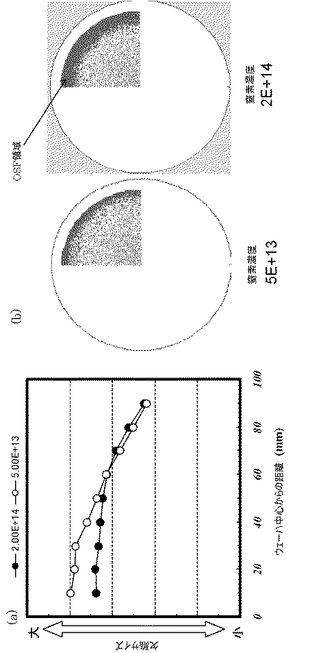
図1,表1に示すように、酸素濃度8ppmaの場合には、熱処理を行っても、特にバルク中に欠陥が残ってしまい、バルク中の欠陥密度を2×10⁶/cm3以下とすることはできなかった。一方、4、6ppmaの場合には、欠陥密度は2×106/cm3以下となり、特に5ppma以下の場合には、バルク中にも欠陥が検出されなかった。従って、酸素濃度は7ppma未満、特には5ppma以下が好ましいことが分かる。 As shown in FIG. 1 and Table 1, when the oxygen concentration is 8 ppma, defects remain particularly in the bulk even when heat treatment is performed, and the defect density in the bulk is set to 2 × 10 6 / cm 3 or less. I couldn't. On the other hand, in the case of 4, 6 ppma, the defect density was 2 × 10 6 / cm 3 or less, and in particular, in the case of 5 ppma or less, no defect was detected in the bulk. Therefore, it can be seen that the oxygen concentration is preferably less than 7 ppma, particularly 5 ppma or less.
(実施例2、比較例2)
(窒素濃度の臨界的意義の証明)
チョクラルスキー法により得られた、酸素濃度が4ppma(JEIDA)でV領域のシリコン単結晶ウェーハを、窒素濃度が1×10¹³atoms/cm3未満、2×1013atoms/cm3、5×1013atoms/cm3、2×1014atoms/cm3の4種類用意して、Ar雰囲気下、1170℃、1時間の熱処理を行った。
実施例1、比較例1と同様の方法で欠陥評価を行った結果を表2に示す。
(Example 2, comparative example 2)
(Proof of critical significance of nitrogen concentration)
A silicon single crystal wafer in the V region having an oxygen concentration of 4 ppma (JEIDA) obtained by the Czochralski method has a nitrogen concentration of less than 1 × 10 13 atoms / cm 3 , 2 × 10 13 atoms / cm 3 , 5 × Four types of 10 13 atoms / cm 3 and 2 × 10 14 atoms / cm 3 were prepared, and heat treatment was performed at 1170 ° C. for 1 hour in an Ar atmosphere.
Table 2 shows the results of defect evaluation performed in the same manner as in Example 1 and Comparative Example 1.
表2から分かるように、窒素濃度が1×10¹³atoms/cm3未満の場合には、欠陥のサイズが大きく、熱処理後にも、表層及びバルクに欠陥が残ってしまう。
図2(a)に熱処理前のシリコン単結晶中の欠陥のサイズを示すグラフと、(b)その表面の欠陥領域をMO601で測定した結果を示す。図2(b)に示すように、同じ条件で引き上げた単結晶から得られたウェーハにもかかわらず、窒素濃度が2×10¹⁴atoms/cm3の方は、窒素濃度が過剰で、V領域の外周にOSFが形成されてしまっている。すなわち、図2(a)に示すように、外周部分の欠陥サイズが窒素濃度が2×1014atoms/cm3の場合の方が大きくなっている。このように、窒素濃度が1×1014atoms/cm3を超えると、外周にOSFが形成された。
As can be seen from Table 2, when the nitrogen concentration is less than 1 × 10 13 atoms / cm 3 , the defect size is large, and defects remain in the surface layer and the bulk even after the heat treatment.
FIG. 2A shows a graph showing the size of defects in the silicon single crystal before the heat treatment, and FIG. 2B shows the result of measuring the defect region on the surface by MO601. As shown in FIG. 2B, the nitrogen concentration is 2 × 10 14 atoms / cm 3 in spite of the wafer obtained from the single crystal pulled up under the same conditions. OSF has been formed on the outer periphery of the substrate. That is, as shown in FIG. 2A, the defect size in the outer peripheral portion is larger when the nitrogen concentration is 2 × 10 14 atoms / cm 3 . Thus, when the nitrogen concentration exceeded 1 × 10 14 atoms / cm 3 , OSF was formed on the outer periphery.
(実施例3、比較例3)
チョクラルスキー法により得られた、窒素濃度が5×10¹³atoms/cm3、酸素濃度が4ppma(JEIDA)でV領域のシリコン単結晶ウェーハを用意して、Ar雰囲気下、1時間の熱処理を行った。熱処理温度は1130、1150、1170、1200、1300℃より高い温度(>1300℃)でそれぞれ行った。
実施例1、比較例1と同様の方法で欠陥評価を行った。また、面内抵抗率分布を平面SRで測定した。結果を表3に示す。
(Example 3, Comparative Example 3)
A V-region silicon single crystal wafer having a nitrogen concentration of 5 × 10 13 atoms / cm 3 and an oxygen concentration of 4 ppma (JEIDA) obtained by the Czochralski method is prepared and heat-treated for 1 hour in an Ar atmosphere. went. The heat treatment temperatures were higher than 1130, 1150, 1170, 1200 and 1300 ° C. (> 1300 ° C.), respectively.
Defect evaluation was performed in the same manner as in Example 1 and Comparative Example 1. Further, the in-plane resistivity distribution was measured on the plane SR. The results are shown in Table 3.
表3に示すように、熱処理温度が1130℃では、欠陥が残ってしまっており、また、抵抗率の均一化も不十分である。一方、1150〜1200℃では欠陥が消滅し、抵抗率が均一になっている。また、熱処理温度が1300℃より高いと、スリップ転位が発生してしまった。 As shown in Table 3, when the heat treatment temperature is 1130 ° C., defects remain, and the resistivity is not sufficiently uniform. On the other hand, at 1150 to 1200 ° C., the defect disappears and the resistivity is uniform. Further, when the heat treatment temperature was higher than 1300 ° C., slip dislocation occurred.
なお、本発明は、上記実施形態に限定されるものではない。上記実施形態は、例示であり、本発明の特許請求の範囲に記載された技術的思想と実質的に同一な構成を有し、同様な作用効果を奏するものは、いかなるものであっても本発明の技術的範囲に包含される。 The present invention is not limited to the above embodiment. The above-described embodiment is an exemplification, and the present invention has substantially the same configuration as the technical idea described in the claims of the present invention, and any device that exhibits the same function and effect is the present invention. It is included in the technical scope of the invention.
Claims (7)
The annealed wafer according to claim 5 or 6, wherein the annealed wafer has an N conductivity type and is used for an IGBT device.
Priority Applications (6)
| Application Number | Priority Date | Filing Date | Title |
|---|---|---|---|
| JP2011011790A JP5764937B2 (en) | 2011-01-24 | 2011-01-24 | Manufacturing method of silicon single crystal wafer |
| US13/993,810 US8916953B2 (en) | 2011-01-24 | 2012-01-06 | Method for manufacturing silicon single crystal wafer and annealed wafer |
| DE112012000306.3T DE112012000306B4 (en) | 2011-01-24 | 2012-01-06 | Method for manufacturing a silicon single crystal wafer |
| CN201280006313.7A CN103328696B (en) | 2011-01-24 | 2012-01-06 | The manufacture method of silicon single crystal wafer and annealed wafer |
| PCT/JP2012/000053 WO2012101957A1 (en) | 2011-01-24 | 2012-01-06 | Silicon single-crystal wafer production method, and annealed wafer |
| KR1020137019428A KR101750688B1 (en) | 2011-01-24 | 2012-01-06 | Silicon single-crystal wafer production method, and annealed wafer |
Applications Claiming Priority (1)
| Application Number | Priority Date | Filing Date | Title |
|---|---|---|---|
| JP2011011790A JP5764937B2 (en) | 2011-01-24 | 2011-01-24 | Manufacturing method of silicon single crystal wafer |
Publications (2)
| Publication Number | Publication Date |
|---|---|
| JP2012153548A true JP2012153548A (en) | 2012-08-16 |
| JP5764937B2 JP5764937B2 (en) | 2015-08-19 |
Family
ID=46580538
Family Applications (1)
| Application Number | Title | Priority Date | Filing Date |
|---|---|---|---|
| JP2011011790A Active JP5764937B2 (en) | 2011-01-24 | 2011-01-24 | Manufacturing method of silicon single crystal wafer |
Country Status (6)
| Country | Link |
|---|---|
| US (1) | US8916953B2 (en) |
| JP (1) | JP5764937B2 (en) |
| KR (1) | KR101750688B1 (en) |
| CN (1) | CN103328696B (en) |
| DE (1) | DE112012000306B4 (en) |
| WO (1) | WO2012101957A1 (en) |
Cited By (5)
| Publication number | Priority date | Publication date | Assignee | Title |
|---|---|---|---|---|
| WO2014061196A1 (en) * | 2012-10-16 | 2014-04-24 | 信越半導体株式会社 | Soi wafer manufacturing method |
| WO2014080565A1 (en) * | 2012-11-26 | 2014-05-30 | 信越半導体株式会社 | Soi wafer manufacturing method |
| JP2014148448A (en) * | 2013-02-01 | 2014-08-21 | Shin Etsu Handotai Co Ltd | Silicon single crystal wafer, evaluation method thereof and method for manufacturing silicon single crystal rod |
| WO2015107874A1 (en) * | 2014-01-16 | 2015-07-23 | 信越半導体株式会社 | Heat-treatment method for single-crystal silicon wafer |
| WO2015107875A1 (en) * | 2014-01-16 | 2015-07-23 | 信越半導体株式会社 | Heat-treatment method for single-crystal silicon wafer |
Families Citing this family (7)
| Publication number | Priority date | Publication date | Assignee | Title |
|---|---|---|---|---|
| KR101303422B1 (en) * | 2011-03-28 | 2013-09-05 | 주식회사 엘지실트론 | Method for Manufacturing Single Crystal Ingot and Single Crystal Ingot, Wafer manufactured by the same |
| DE102014107161B4 (en) * | 2014-05-21 | 2019-10-31 | Infineon Technologies Ag | Method of making an IGBT and IGBT |
| DE102016209008B4 (en) * | 2016-05-24 | 2019-10-02 | Siltronic Ag | Process for producing a semiconductor wafer of monocrystalline silicon, apparatus for producing a semiconductor wafer of monocrystalline silicon and semiconductor wafer of monocrystalline silicon |
| CN106591948B (en) * | 2017-01-21 | 2019-10-25 | 台州市一能科技有限公司 | A kind of N-type polycrystalline silicon used for solar batteries and its production method |
| KR102092358B1 (en) | 2018-06-22 | 2020-03-23 | 울산과학기술원 | Single Crystal Ingot using Barium Zirconate and a Method of Manufacturing thereof |
| JP7099175B2 (en) * | 2018-08-27 | 2022-07-12 | 株式会社Sumco | Silicon single crystal manufacturing method and silicon wafer |
| CN114990693A (en) * | 2022-04-02 | 2022-09-02 | 天津中环领先材料技术有限公司 | Annealing process of NTD monocrystalline silicon |
Citations (2)
| Publication number | Priority date | Publication date | Assignee | Title |
|---|---|---|---|---|
| JP2001146498A (en) * | 1999-11-12 | 2001-05-29 | Shin Etsu Handotai Co Ltd | Silicon single crystal wafer, method for producing the same and soi wafer |
| WO2009025342A1 (en) * | 2007-08-21 | 2009-02-26 | Sumco Corporation | Silicon single crystal wafer for igbt and method for manufacturing silicon single crystal wafer for igbt |
Family Cites Families (20)
| Publication number | Priority date | Publication date | Assignee | Title |
|---|---|---|---|---|
| JPS5321460B2 (en) * | 1974-06-06 | 1978-07-03 | ||
| TW589415B (en) * | 1998-03-09 | 2004-06-01 | Shinetsu Handotai Kk | Method for producing silicon single crystal wafer and silicon single crystal wafer |
| JP2000020399A (en) * | 1998-06-30 | 2000-01-21 | Hitachi Ltd | Virtual computer system |
| JP3800006B2 (en) * | 1998-08-31 | 2006-07-19 | 信越半導体株式会社 | Manufacturing method of silicon single crystal wafer and silicon single crystal wafer |
| US6517632B2 (en) * | 2000-01-17 | 2003-02-11 | Toshiba Ceramics Co., Ltd. | Method of fabricating a single crystal ingot and method of fabricating a silicon wafer |
| JP2002201091A (en) * | 2000-09-01 | 2002-07-16 | Wacker Nsce Corp | Method of manufacturing epitaxial wafer having no epitaxial defect using nitrogen and carbon added substrate |
| JP4463957B2 (en) | 2000-09-20 | 2010-05-19 | 信越半導体株式会社 | Silicon wafer manufacturing method and silicon wafer |
| US7189293B2 (en) | 2001-06-28 | 2007-03-13 | Shin-Etsu Handotai Co., Ltd. | Method of producing annealed wafer and annealed wafer |
| JP4633977B2 (en) | 2001-08-30 | 2011-02-16 | 信越半導体株式会社 | Annealed wafer manufacturing method and annealed wafer |
| JP4703934B2 (en) | 2002-02-26 | 2011-06-15 | 信越半導体株式会社 | Annealed wafer manufacturing method |
| DE102005013831B4 (en) * | 2005-03-24 | 2008-10-16 | Siltronic Ag | Silicon wafer and method for the thermal treatment of a silicon wafer |
| JP5188673B2 (en) * | 2005-06-09 | 2013-04-24 | 株式会社Sumco | Silicon wafer for IGBT and method for manufacturing the same |
| JP2007194232A (en) * | 2006-01-17 | 2007-08-02 | Shin Etsu Handotai Co Ltd | Process for producing silicon single crystal wafer |
| JP4760729B2 (en) * | 2006-02-21 | 2011-08-31 | 株式会社Sumco | Silicon single crystal wafer for IGBT and manufacturing method of silicon single crystal wafer for IGBT |
| JP5072460B2 (en) * | 2006-09-20 | 2012-11-14 | ジルトロニック アクチエンゲゼルシャフト | Silicon wafer for semiconductor and manufacturing method thereof |
| EP2144280B1 (en) * | 2007-05-02 | 2010-12-29 | Siltronic AG | Silicon wafer and method for manufacturing the same |
| JP5321460B2 (en) | 2007-08-21 | 2013-10-23 | 株式会社Sumco | Manufacturing method of silicon single crystal wafer for IGBT |
| WO2009025338A1 (en) | 2007-08-21 | 2009-02-26 | Sumco Corporation | Silicon single crystal wafer for igbt and method for manufacturing silicon single crystal wafer for igbt |
| WO2009028658A1 (en) | 2007-08-29 | 2009-03-05 | Sumco Corporation | Silicon single crystal wafer for igbt, method for manufacturing silicon single crystal wafer for igbt and method for assuring resistivity of silicon single crystal wafer for igbt |
| JP2010062466A (en) * | 2008-09-05 | 2010-03-18 | Sumco Corp | Silicon wafer for vertical silicon device and its manufacturing method, silicon single crystal, and vertical silicon device |
-
2011
- 2011-01-24 JP JP2011011790A patent/JP5764937B2/en active Active
-
2012
- 2012-01-06 CN CN201280006313.7A patent/CN103328696B/en active Active
- 2012-01-06 WO PCT/JP2012/000053 patent/WO2012101957A1/en active Application Filing
- 2012-01-06 US US13/993,810 patent/US8916953B2/en active Active
- 2012-01-06 KR KR1020137019428A patent/KR101750688B1/en active IP Right Grant
- 2012-01-06 DE DE112012000306.3T patent/DE112012000306B4/en active Active
Patent Citations (2)
| Publication number | Priority date | Publication date | Assignee | Title |
|---|---|---|---|---|
| JP2001146498A (en) * | 1999-11-12 | 2001-05-29 | Shin Etsu Handotai Co Ltd | Silicon single crystal wafer, method for producing the same and soi wafer |
| WO2009025342A1 (en) * | 2007-08-21 | 2009-02-26 | Sumco Corporation | Silicon single crystal wafer for igbt and method for manufacturing silicon single crystal wafer for igbt |
Cited By (16)
| Publication number | Priority date | Publication date | Assignee | Title |
|---|---|---|---|---|
| WO2014061196A1 (en) * | 2012-10-16 | 2014-04-24 | 信越半導体株式会社 | Soi wafer manufacturing method |
| JP2014082316A (en) * | 2012-10-16 | 2014-05-08 | Shin Etsu Handotai Co Ltd | Soi wafer manufacturing method |
| WO2014080565A1 (en) * | 2012-11-26 | 2014-05-30 | 信越半導体株式会社 | Soi wafer manufacturing method |
| JP2014107357A (en) * | 2012-11-26 | 2014-06-09 | Shin Etsu Handotai Co Ltd | Soi wafer manufacturing method |
| JP2014148448A (en) * | 2013-02-01 | 2014-08-21 | Shin Etsu Handotai Co Ltd | Silicon single crystal wafer, evaluation method thereof and method for manufacturing silicon single crystal rod |
| WO2015107874A1 (en) * | 2014-01-16 | 2015-07-23 | 信越半導体株式会社 | Heat-treatment method for single-crystal silicon wafer |
| WO2015107875A1 (en) * | 2014-01-16 | 2015-07-23 | 信越半導体株式会社 | Heat-treatment method for single-crystal silicon wafer |
| JP2015135872A (en) * | 2014-01-16 | 2015-07-27 | 信越半導体株式会社 | Silicon single crystal wafer heat treatment method |
| JP2015135873A (en) * | 2014-01-16 | 2015-07-27 | 信越半導体株式会社 | Silicon single crystal wafer heat treatment method |
| KR20160106602A (en) * | 2014-01-16 | 2016-09-12 | 신에쯔 한도타이 가부시키가이샤 | Heat-treatment method for single-crystal silicon wafer |
| KR20160107169A (en) * | 2014-01-16 | 2016-09-13 | 신에쯔 한도타이 가부시키가이샤 | Heat-treatment method for single-crystal silicon wafer |
| US9850595B2 (en) | 2014-01-16 | 2017-12-26 | Shin-Etsu Handotai Co., Ltd. | Method for heat treatment of silicon single crystal wafer |
| US9938640B2 (en) | 2014-01-16 | 2018-04-10 | Shin-Etsu Handotai Co., Ltd. | Method for heat treatment of silicon single crystal wafer |
| US10066322B2 (en) | 2014-01-16 | 2018-09-04 | Shin-Etsu Handotai Co., Ltd. | Method for heat treatment of silicon single crystal wafer |
| KR102188589B1 (en) * | 2014-01-16 | 2020-12-08 | 신에쯔 한도타이 가부시키가이샤 | Heat-treatment method for single-crystal silicon wafer |
| KR102192287B1 (en) * | 2014-01-16 | 2020-12-17 | 신에쯔 한도타이 가부시키가이샤 | Heat-treatment method for single-crystal silicon wafer |
Also Published As
| Publication number | Publication date |
|---|---|
| WO2012101957A1 (en) | 2012-08-02 |
| US8916953B2 (en) | 2014-12-23 |
| DE112012000306T5 (en) | 2013-09-26 |
| US20130264685A1 (en) | 2013-10-10 |
| KR20140016255A (en) | 2014-02-07 |
| KR101750688B1 (en) | 2017-06-26 |
| CN103328696A (en) | 2013-09-25 |
| DE112012000306B4 (en) | 2021-03-18 |
| CN103328696B (en) | 2016-05-11 |
| JP5764937B2 (en) | 2015-08-19 |
Similar Documents
| Publication | Publication Date | Title |
|---|---|---|
| JP5764937B2 (en) | Manufacturing method of silicon single crystal wafer | |
| JP5621791B2 (en) | Manufacturing method of silicon single crystal wafer and electronic device | |
| JP2006344823A (en) | Silicon wafer for igbt and its manufacturing method | |
| JPWO2004073057A1 (en) | Silicon wafer manufacturing method | |
| JP5251137B2 (en) | Single crystal silicon wafer and manufacturing method thereof | |
| JP2007207875A (en) | Silicon wafer and manufacturing method thereof | |
| JP5103745B2 (en) | High frequency diode and manufacturing method thereof | |
| JP5885305B2 (en) | Silicon wafer and manufacturing method thereof | |
| JP2008294112A (en) | Silicon single-crystal wafer and method of manufacturing the same | |
| KR102188589B1 (en) | Heat-treatment method for single-crystal silicon wafer | |
| JP2010056316A (en) | Silicon wafer, and method of manufacturing the same | |
| JP2010287885A (en) | Silicon wafer and method of manufacturing the same | |
| WO2014057741A1 (en) | Method for producing silicon epitaxial wafer and solid-state image-pickup element using same | |
| KR102192287B1 (en) | Heat-treatment method for single-crystal silicon wafer | |
| JP2013219300A (en) | Epitaxial wafer and manufacturing method of the same | |
| JP5906006B2 (en) | Silicon wafer manufacturing method | |
| JP5560546B2 (en) | Silicon wafer and manufacturing method thereof | |
| JP2016195211A (en) | Silicon wafer manufacturing method | |
| JP2012134517A (en) | Silicon wafer for igbt and manufacturing method of the same | |
| WO2021166896A1 (en) | Method for manufacturing semiconductor silicon wafer | |
| JP2013089783A (en) | Manufacturing method of silicon wafer | |
| JP6988737B2 (en) | Manufacturing method of silicon wafer and silicon wafer | |
| TW201802305A (en) | Silicon wafer | |
| JP5805843B2 (en) | Silicon single crystal substrate and manufacturing method thereof | |
| JP5434239B2 (en) | Silicon wafer manufacturing method |
Legal Events
| Date | Code | Title | Description |
|---|---|---|---|
| A621 | Written request for application examination |
Free format text: JAPANESE INTERMEDIATE CODE: A621 Effective date: 20121218 |
|
| A131 | Notification of reasons for refusal |
Free format text: JAPANESE INTERMEDIATE CODE: A131 Effective date: 20140603 |
|
| A521 | Request for written amendment filed |
Free format text: JAPANESE INTERMEDIATE CODE: A523 Effective date: 20140711 |
|
| A02 | Decision of refusal |
Free format text: JAPANESE INTERMEDIATE CODE: A02 Effective date: 20141216 |
|
| A521 | Request for written amendment filed |
Free format text: JAPANESE INTERMEDIATE CODE: A523 Effective date: 20150306 |
|
| A911 | Transfer to examiner for re-examination before appeal (zenchi) |
Free format text: JAPANESE INTERMEDIATE CODE: A911 Effective date: 20150316 |
|
| TRDD | Decision of grant or rejection written | ||
| A01 | Written decision to grant a patent or to grant a registration (utility model) |
Free format text: JAPANESE INTERMEDIATE CODE: A01 Effective date: 20150519 |
|
| A61 | First payment of annual fees (during grant procedure) |
Free format text: JAPANESE INTERMEDIATE CODE: A61 Effective date: 20150601 |
|
| R150 | Certificate of patent or registration of utility model |
Ref document number: 5764937 Country of ref document: JP Free format text: JAPANESE INTERMEDIATE CODE: R150 |
|
| S531 | Written request for registration of change of domicile |
Free format text: JAPANESE INTERMEDIATE CODE: R313531 |
|
| R350 | Written notification of registration of transfer |
Free format text: JAPANESE INTERMEDIATE CODE: R350 |
|
| R250 | Receipt of annual fees |
Free format text: JAPANESE INTERMEDIATE CODE: R250 |
|
| R250 | Receipt of annual fees |
Free format text: JAPANESE INTERMEDIATE CODE: R250 |
|
| R250 | Receipt of annual fees |
Free format text: JAPANESE INTERMEDIATE CODE: R250 |
|
| R250 | Receipt of annual fees |
Free format text: JAPANESE INTERMEDIATE CODE: R250 |
|
| R250 | Receipt of annual fees |
Free format text: JAPANESE INTERMEDIATE CODE: R250 |
|
| R250 | Receipt of annual fees |
Free format text: JAPANESE INTERMEDIATE CODE: R250 |