JP2012146977A - Semiconductor device including diode - Google Patents
Semiconductor device including diode Download PDFInfo
- Publication number
- JP2012146977A JP2012146977A JP2011282710A JP2011282710A JP2012146977A JP 2012146977 A JP2012146977 A JP 2012146977A JP 2011282710 A JP2011282710 A JP 2011282710A JP 2011282710 A JP2011282710 A JP 2011282710A JP 2012146977 A JP2012146977 A JP 2012146977A
- Authority
- JP
- Japan
- Prior art keywords
- region
- type
- anode
- semiconductor
- semiconductor device
- Prior art date
- Legal status (The legal status is an assumption and is not a legal conclusion. Google has not performed a legal analysis and makes no representation as to the accuracy of the status listed.)
- Granted
Links
- 239000004065 semiconductor Substances 0.000 title claims abstract description 102
- 239000012535 impurity Substances 0.000 claims description 26
- 238000002955 isolation Methods 0.000 claims description 12
- 230000005669 field effect Effects 0.000 claims description 10
- 239000000758 substrate Substances 0.000 claims description 7
- 230000000903 blocking effect Effects 0.000 claims description 5
- 238000011084 recovery Methods 0.000 abstract description 10
- 239000002184 metal Substances 0.000 description 8
- 239000002800 charge carrier Substances 0.000 description 7
- 239000007943 implant Substances 0.000 description 4
- 238000010586 diagram Methods 0.000 description 3
- 230000000694 effects Effects 0.000 description 3
- 238000000034 method Methods 0.000 description 3
- 239000000956 alloy Substances 0.000 description 2
- 229910045601 alloy Inorganic materials 0.000 description 2
- 238000005530 etching Methods 0.000 description 2
- 238000009413 insulation Methods 0.000 description 2
- 229910004298 SiO 2 Inorganic materials 0.000 description 1
- VYPSYNLAJGMNEJ-UHFFFAOYSA-N Silicium dioxide Chemical compound O=[Si]=O VYPSYNLAJGMNEJ-UHFFFAOYSA-N 0.000 description 1
- 230000004913 activation Effects 0.000 description 1
- 230000006978 adaptation Effects 0.000 description 1
- 239000012620 biological material Substances 0.000 description 1
- 239000002019 doping agent Substances 0.000 description 1
- 238000001312 dry etching Methods 0.000 description 1
- 239000011810 insulating material Substances 0.000 description 1
- 239000012212 insulator Substances 0.000 description 1
- 238000005468 ion implantation Methods 0.000 description 1
- 239000000463 material Substances 0.000 description 1
- 229910052814 silicon oxide Inorganic materials 0.000 description 1
- 238000006467 substitution reaction Methods 0.000 description 1
Images


Classifications
-
- H—ELECTRICITY
- H01—ELECTRIC ELEMENTS
- H01L—SEMICONDUCTOR DEVICES NOT COVERED BY CLASS H10
- H01L27/00—Devices consisting of a plurality of semiconductor or other solid-state components formed in or on a common substrate
- H01L27/02—Devices consisting of a plurality of semiconductor or other solid-state components formed in or on a common substrate including semiconductor components specially adapted for rectifying, oscillating, amplifying or switching and having at least one potential-jump barrier or surface barrier; including integrated passive circuit elements with at least one potential-jump barrier or surface barrier
- H01L27/04—Devices consisting of a plurality of semiconductor or other solid-state components formed in or on a common substrate including semiconductor components specially adapted for rectifying, oscillating, amplifying or switching and having at least one potential-jump barrier or surface barrier; including integrated passive circuit elements with at least one potential-jump barrier or surface barrier the substrate being a semiconductor body
- H01L27/08—Devices consisting of a plurality of semiconductor or other solid-state components formed in or on a common substrate including semiconductor components specially adapted for rectifying, oscillating, amplifying or switching and having at least one potential-jump barrier or surface barrier; including integrated passive circuit elements with at least one potential-jump barrier or surface barrier the substrate being a semiconductor body including only semiconductor components of a single kind
- H01L27/0814—Diodes only
-
- H—ELECTRICITY
- H01—ELECTRIC ELEMENTS
- H01L—SEMICONDUCTOR DEVICES NOT COVERED BY CLASS H10
- H01L27/00—Devices consisting of a plurality of semiconductor or other solid-state components formed in or on a common substrate
- H01L27/02—Devices consisting of a plurality of semiconductor or other solid-state components formed in or on a common substrate including semiconductor components specially adapted for rectifying, oscillating, amplifying or switching and having at least one potential-jump barrier or surface barrier; including integrated passive circuit elements with at least one potential-jump barrier or surface barrier
- H01L27/04—Devices consisting of a plurality of semiconductor or other solid-state components formed in or on a common substrate including semiconductor components specially adapted for rectifying, oscillating, amplifying or switching and having at least one potential-jump barrier or surface barrier; including integrated passive circuit elements with at least one potential-jump barrier or surface barrier the substrate being a semiconductor body
- H01L27/06—Devices consisting of a plurality of semiconductor or other solid-state components formed in or on a common substrate including semiconductor components specially adapted for rectifying, oscillating, amplifying or switching and having at least one potential-jump barrier or surface barrier; including integrated passive circuit elements with at least one potential-jump barrier or surface barrier the substrate being a semiconductor body including a plurality of individual components in a non-repetitive configuration
- H01L27/0611—Devices consisting of a plurality of semiconductor or other solid-state components formed in or on a common substrate including semiconductor components specially adapted for rectifying, oscillating, amplifying or switching and having at least one potential-jump barrier or surface barrier; including integrated passive circuit elements with at least one potential-jump barrier or surface barrier the substrate being a semiconductor body including a plurality of individual components in a non-repetitive configuration integrated circuits having a two-dimensional layout of components without a common active region
- H01L27/0617—Devices consisting of a plurality of semiconductor or other solid-state components formed in or on a common substrate including semiconductor components specially adapted for rectifying, oscillating, amplifying or switching and having at least one potential-jump barrier or surface barrier; including integrated passive circuit elements with at least one potential-jump barrier or surface barrier the substrate being a semiconductor body including a plurality of individual components in a non-repetitive configuration integrated circuits having a two-dimensional layout of components without a common active region comprising components of the field-effect type
- H01L27/0629—Devices consisting of a plurality of semiconductor or other solid-state components formed in or on a common substrate including semiconductor components specially adapted for rectifying, oscillating, amplifying or switching and having at least one potential-jump barrier or surface barrier; including integrated passive circuit elements with at least one potential-jump barrier or surface barrier the substrate being a semiconductor body including a plurality of individual components in a non-repetitive configuration integrated circuits having a two-dimensional layout of components without a common active region comprising components of the field-effect type in combination with diodes, or resistors, or capacitors
-
- H—ELECTRICITY
- H01—ELECTRIC ELEMENTS
- H01L—SEMICONDUCTOR DEVICES NOT COVERED BY CLASS H10
- H01L29/00—Semiconductor devices adapted for rectifying, amplifying, oscillating or switching, or capacitors or resistors with at least one potential-jump barrier or surface barrier, e.g. PN junction depletion layer or carrier concentration layer; Details of semiconductor bodies or of electrodes thereof ; Multistep manufacturing processes therefor
- H01L29/66—Types of semiconductor device ; Multistep manufacturing processes therefor
- H01L29/68—Types of semiconductor device ; Multistep manufacturing processes therefor controllable by only the electric current supplied, or only the electric potential applied, to an electrode which does not carry the current to be rectified, amplified or switched
- H01L29/70—Bipolar devices
- H01L29/72—Transistor-type devices, i.e. able to continuously respond to applied control signals
- H01L29/739—Transistor-type devices, i.e. able to continuously respond to applied control signals controlled by field-effect, e.g. bipolar static induction transistors [BSIT]
- H01L29/7393—Insulated gate bipolar mode transistors, i.e. IGBT; IGT; COMFET
- H01L29/7395—Vertical transistors, e.g. vertical IGBT
- H01L29/7396—Vertical transistors, e.g. vertical IGBT with a non planar surface, e.g. with a non planar gate or with a trench or recess or pillar in the surface of the emitter, base or collector region for improving current density or short circuiting the emitter and base regions
- H01L29/7397—Vertical transistors, e.g. vertical IGBT with a non planar surface, e.g. with a non planar gate or with a trench or recess or pillar in the surface of the emitter, base or collector region for improving current density or short circuiting the emitter and base regions and a gate structure lying on a slanted or vertical surface or formed in a groove, e.g. trench gate IGBT
-
- H—ELECTRICITY
- H01—ELECTRIC ELEMENTS
- H01L—SEMICONDUCTOR DEVICES NOT COVERED BY CLASS H10
- H01L29/00—Semiconductor devices adapted for rectifying, amplifying, oscillating or switching, or capacitors or resistors with at least one potential-jump barrier or surface barrier, e.g. PN junction depletion layer or carrier concentration layer; Details of semiconductor bodies or of electrodes thereof ; Multistep manufacturing processes therefor
- H01L29/66—Types of semiconductor device ; Multistep manufacturing processes therefor
- H01L29/86—Types of semiconductor device ; Multistep manufacturing processes therefor controllable only by variation of the electric current supplied, or only the electric potential applied, to one or more of the electrodes carrying the current to be rectified, amplified, oscillated or switched
- H01L29/861—Diodes
- H01L29/8611—Planar PN junction diodes
-
- H—ELECTRICITY
- H01—ELECTRIC ELEMENTS
- H01L—SEMICONDUCTOR DEVICES NOT COVERED BY CLASS H10
- H01L2924/00—Indexing scheme for arrangements or methods for connecting or disconnecting semiconductor or solid-state bodies as covered by H01L24/00
- H01L2924/0001—Technical content checked by a classifier
- H01L2924/0002—Not covered by any one of groups H01L24/00, H01L24/00 and H01L2224/00
Abstract
Description
半導体ダイオードは半導体用途において広く使用されている。半導体変換器用途では、還流ダイオードの逆回復挙動とオン状態特性とのトレードオフが変換器特性に影響を与える。したがってダイオードの逆回復挙動とオン状態特性とのトレードオフを改善することが望ましい。 Semiconductor diodes are widely used in semiconductor applications. In semiconductor converter applications, the trade-off between reverse recovery behavior and on-state characteristics of the freewheeling diode affects the converter characteristics. It is therefore desirable to improve the trade-off between diode reverse recovery behavior and on-state characteristics.
半導体装置の一実施形態によると、半導体装置は陰極を含む。半導体装置はさらに第1のp型半導体陽極領域と第2のp型半導体陽極領域とを有する陽極を含む。第1のp型半導体陽極領域は陽極接触領域に電気的に接続される。第2のp型半導体陽極領域は、第2のp型半導体陽極領域と陽極接触領域間を電気的に接続または切断するように構成されたスイッチを介し陽極接触領域に電気的に接続される。 According to one embodiment of the semiconductor device, the semiconductor device includes a cathode. The semiconductor device further includes an anode having a first p-type semiconductor anode region and a second p-type semiconductor anode region. The first p-type semiconductor anode region is electrically connected to the anode contact region. The second p-type semiconductor anode region is electrically connected to the anode contact region via a switch configured to electrically connect or disconnect between the second p-type semiconductor anode region and the anode contact region.
当業者は、以下の詳細な説明を読み添付図面を見ることによりさらなる特徴と利点を理解することになる。 Those skilled in the art will appreciate further features and advantages upon reading the following detailed description and viewing the accompanying drawings.
添付図面は本発明をさらに理解するために含まれ、本明細書に援用され本明細書の一部を構成する。添付図面は本発明の実施形態を例示し、本明細書と共に本発明の実施形態の原理を説明するのに役立つ。本発明の他の実施形態および本発明の実施形態の意図した利点の多くは以下の詳細説明を参照することによりさらに良く理解されるので容易に理解される。添付図面の構成要素同士は互いに対して必ずしも一定のスケールで記載されていない。同様な参照符号は対応する同様な部分を示す。様々な例示実施形態の特徴は互いに排除しない限り組み合わせられ得る。 The accompanying drawings are included to provide a further understanding of the invention, and are incorporated in and constitute a part of this specification. The accompanying drawings illustrate embodiments of the invention and, together with the description, serve to explain the principles of embodiments of the invention. Many of the intended advantages of other embodiments of the present invention and embodiments of the present invention will be readily understood as they are better understood by reference to the following detailed description. The components of the accompanying drawings are not necessarily drawn to scale relative to each other. Like reference numerals designate corresponding similar parts. The features of the various exemplary embodiments may be combined unless excluded from one another.
実施形態は添付図面に示され、以下の明細書の中で詳述される。 Embodiments are illustrated in the accompanying drawings and are described in detail in the following specification.
以下の詳細説明では、本明細書の一部をなす添付図面を参照して、本発明を実施し得る特定の実施態様を例示として示す。この点に関し、「最上部」、「最下部」、「前部」「後部」、「先頭の」、「後続の」等の方向用語は説明される図面の配向に関連して使用される。実施形態の構成要素は多くの異なる配向で配置されることができるので、上記方向用語は例示のために使用され、決して限定するものではない。他の実施形態を利用してもよいことと、本発明の範囲から逸脱することなく構造的または論理的変更をなし得ることと、を理解すべきである。したがって以下の詳細説明は限定的な意味でとらえるべきでなく、本発明の範囲は添付の特許請求範囲により規定される。 In the following detailed description, reference is made to the accompanying drawings that form a part hereof, and in which is shown by way of illustration specific embodiments in which the invention may be practiced. In this regard, directional terms such as “top”, “bottom”, “front”, “back”, “top”, “follow” are used in connection with the orientation of the drawings being described. Since the components of the embodiments can be arranged in many different orientations, the above directional terms are used for illustration and are in no way limiting. It should be understood that other embodiments may be utilized and that structural or logical changes may be made without departing from the scope of the present invention. The following detailed description is, therefore, not to be taken in a limiting sense, and the scope of the present invention is defined by the appended claims.
多くの実施形態について以下に説明する。この場合、同一の構造的特徴部は添付図面内の同一または類似の参照符号により特定される。本明細書との関連では、「横の」または「横方向」は、半導体材料または半導体キャリアの横方向の広がりに概して平行に走る方向または広がりを意味するように理解すべきである。したがって横方向はこれらの表面または面に対し概して平行に延びる。これとは対照的に、用語「垂直の」または「垂直方向」はこれらの表面または面、したがって横方向に対して概して垂直に走る方向を意味するように理解される。したがって垂直方向は半導体キャリアの厚さ方向に走る。 A number of embodiments are described below. In this case, identical structural features are identified by identical or similar reference signs in the accompanying drawings. In the context of this specification, “lateral” or “lateral” should be understood to mean a direction or extent that runs generally parallel to the lateral extent of the semiconductor material or semiconductor carrier. The transverse direction thus extends generally parallel to these surfaces or planes. In contrast, the term “vertical” or “vertical direction” is understood to mean a direction that runs generally perpendicular to these surfaces or planes, and thus transverse directions. Therefore, the vertical direction runs in the thickness direction of the semiconductor carrier.
図1に、陽極Aと陰極Cを含むダイオード100の一実施形態の概略図を例示する。陽極Aは第1の陽極A1と第2の陽極A2を含む。第1の陽極A1は陽極接触部(図1に図示せず)に電気的に接続される。第2の陽極A2は、第2の陽極A2と陽極接触部間を電気的に接続または切断するように構成されたスイッチSを介し陽極接触部に電気的に接続される。
FIG. 1 illustrates a schematic diagram of one embodiment of a
スイッチSは、オン状態(すなわち導電状態)とオフ状態(すなわち非導電状態)間で切り替わるのに好適な任意の装置であってよい。一例として、スイッチSはFETまたはバイポーラトランジスタ等のトランジスタを含んでよい。 Switch S may be any device suitable for switching between an on state (ie, a conductive state) and an off state (ie, a non-conductive state). As an example, the switch S may include a transistor such as an FET or a bipolar transistor.
一実施形態によると、スイッチSは、ダイオード100の活性領域内に少なくとも部分的に形成されてもよい。一例として、第2の陽極A2は、ダイオード100とスイッチSの両方に共通の半導体領域、例えば第2の陽極とFET(バイポーラトランジスタ)のソースとドレイン(エミッタとコレクタ)の1つを構成するp型半導体領域を含んでよい。別の実施形態によると、スイッチSはダイオード100の活性領域と異なる活性領域内に形成されてもよい。一例として、第2の陽極A2は接触プラグおよび/または配線を介しスイッチSに電気的に接続されてもよいし、スイッチSは他の接触プラグおよび/または別の配線を介し陽極接触部に電気的に接続されてもよい。陰極Cは、第1の陽極A1と第2の陽極A2の両方に共通な陰極接触部例えば金属領域を含む。
According to one embodiment, the switch S may be at least partially formed in the active region of the
スイッチSがオン状態(すなわち導電状態)である場合、第2の陽極A2は陽極Aと陰極C間の電流の流れに寄与する。スイッチSがオフ状態にある場合、陰極Cと第2の陽極A2間の電流の流れは無効にされる。陽極効率は、不純物添加のドーズ量(例えば、不純物濃度、不純物添加の垂直方向広がり、または陽極A内の少数キャリア寿命)等の効率に影響を与える陽極パラメータを適切に調整することにより、第1の陽極A1より第2の陽極A2においてより高く設定される。ダイオード100はスイッチSのオン状態およびオフ状態における電圧をブロッキングすることができる。ダイオード100は、スイッチSがオフ状態にあり第2の陽極A2が非作動化された場合、低い電荷キャリア濃度したがって有用な逆回復挙動を有する所謂高速モードで動作するが、スイッチSがオン状態にあり第2の陽極A2が作動化された場合、ダイオード100は高い電荷キャリア濃度と低オン抵抗を有する所謂低飽和モードで動作する。スイッチSのオフ状態はダイオード100のより良好な逆回復挙動を可能にするが、スイッチSのオン状態はダイオード100のより良好なオン状態特性を可能にする。したがってダイオード100の動作モードに依存するスイッチSのオン状態とオフ状態とを切り替えることにより、ダイオード100の逆回復挙動とオン状態特性とのトレードオフを改善することができる。
When the switch S is in the on state (that is, the conductive state), the second anode A 2 contributes to the current flow between the anode A and the cathode C. If the switch S is in the OFF state, the flow of the cathode C and the second current between the anode A 2 is disabled. The anode efficiency is obtained by appropriately adjusting anode parameters that affect the efficiency such as the dose of impurity addition (for example, impurity concentration, vertical spread of impurity addition, or minority carrier lifetime in the anode A). The second anode A 2 is set higher than the anode A 1 . The
図2に、ダイオード200の一実施形態の一部分の断面を例示する。ダイオード200は、n型半導体基板(例えば、エピタキシャル層等の半導体層をその上に有しない、または1つまたは複数の半導体層を有するSi基板)等のn型ドリフト領域202を含む。n型ドリフト領域202内には、n型ドリフト領域202の第1の側208に接する第1のp型陽極領域204と第2のp型陽極領域206が形成される。n型ドリフト領域202内において、第2のp型陽極領域206の底面は、第1のp型陽極領域204の底面より深くに位置する、すなわち、第1の側208からn型ドリフト領域202への垂直方向210に沿った第2のp型陽極領域206の広がりd2は第1のp型陽極領域204の対応する広がりd1より大きい。横方向211は第1の側208に対して平行であり、垂直方向210に対して垂直である。
FIG. 2 illustrates a cross section of a portion of one embodiment of a
n型陰極領域212は、n型ドリフト領域202の第2の側214でn型ドリフト領域202に接する。n型陰極領域212は第1のp型陽極領域204と第2のp型陽極領域206に共通である。金属または合金等の陰極接触部216はn型陰極領域212に接する。
The n-
第1のp型陽極領域204は第1の側208において陽極接触部218に電気的に接続される。陽極接触部208は1つまたはいくつかの接触プラグおよび/または1つまたはいくつかの配線を含んでよい。
The first p-
第2のp型陽極領域206はFET220を介し陽極接触部218に電気的に接続される。FET220はソースとドレインの一方としてp型陽極領域206を含む。n型領域221はp型陽極領域206内に配置され第1の側208に接する。チャネル222はn型領域221内の第1の側208に位置する。チャネル222の導電率はチャネル222上に配置されたゲート構造224により制御可能である。ゲート構造224は、ゲート誘電体226(例えば、SiO2)とゲート電極228(例えば、金属、合金またはドープ半導体等の導電性または半導体生材料)を含む。FET220のソースとドレインの他方を構成するp型領域230はn型領域221内に配置され第1の側208に接する。FET220のソースとドレイン間の電流の流れは、ゲート電極228にそれぞれの電圧が印加されると、ソースとドレインの一方としての第2のp型陽極領域206とソースとドレインの他方としてのp型領域230との間の第1の側208の横方向211に沿って制御可能である。したがってFET220を介し第2のp型陽極領域206をオンとオフすることによりダイオードの逆回復挙動とオン状態特性に影響を与えることができる。これにより、逆回復挙動とオン状態特性とのトレードオフを改善することができる。
The second p-
第1と第2のp型陽極領域204、206の不純物添加と垂直方向寸法は図2に示す実施形態と異なってもよい。第2のp型陽極領域206の不純物添加のドーズ量は、また、例えば第2のp型陽極領域206内の不純物濃度をそれぞれ増加させることに関連して、第1のp型陽極領域204のn型ドリフト領域202内の深さを第2のp型陽極領域206の深さより大きく設定することにより、第1のp型陽極領域204の不純物添加のドーズ量より大きくしてもよい。第1のp型陽極領域204の不純物添加のドーズ量に対する第2のp型陽極領域206の不純物添加のドーズ量の比は、例えば5〜104、5〜103、または5〜102であってよい。
Impurity addition and vertical dimension of the first and second p-
図3は、図2に示す第1のp型陽極領域204(第2のp型陽極領域206)の線A−A’(B−B’)に沿ったp型不純物の濃度N1(N2)のプロファイルの一実施形態の概略グラフを例示する。 FIG. 3 shows the p-type impurity concentration N 1 (N ′) along the line AA ′ (BB ′) of the first p-type anode region 204 (second p-type anode region 206) shown in FIG. 2 illustrates a schematic graph of an embodiment of the profile of 2 ).
図2の第1のp型陽極領域204内のp型不純物添加の濃度N1は第2のp型陽極領域206内のp型不純物添加の濃度N2より低い。これにより、第2のp型陽極領域206の陽極効率を第1のp型陽極領域204の陽極効率より大きく設定することができる。濃度N1、N2のプロファイルは、例えばエネルギーとドーズ量等のインプラントパラメータを適切に選択することにより調整されてもよい。
The p-type impurity doping concentration N 1 in the first p-
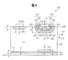
図4は、図2に示す実施形態のダイオード200と類似のダイオード400のさらに別の実施形態の一部分の断面を例示する。しかしながらダイオード400はn型陰極領域412に加え第2のn型陰極領域434という点でダイオード200と異なる。第2のn型陰極領域434は第2のp型陽極領域406に対向して配置されるが、第1のp型陽極領域404に対向した領域には存在しない。さらに、n型ドリフト領域402内において、第2のn型陰極領域434は、n型陰極領域412より深く延びる、すなわち第2の側414からn型ドリフト領域402内への垂直方向410に沿った第2のn型陰極領域434の広がりd4はn型陰極領域412の対応する広がりd3より大きい。これにより陰極効率を、第1のp型陽極領域404に対向した領域よりも第2のp型陽極領域406に対向した領域でより大きく設定することができる。一例としてd4は、例えばインプラントエネルギー等のインプラントパラメータを適切に選択することによりd3より大きくなるように調整されてもよい。
FIG. 4 illustrates a cross-section of a portion of yet another embodiment of a
図5に、図4に示すn型陰極領域412(第2のn型陰極領域434)の線C−C’(D−D’)に沿ったn型不純物の濃度N3(N4)のプロファイルの一実施形態の概略グラフを例示する。 FIG. 5 shows the concentration N 3 (N 4 ) of the n-type impurity along the line CC ′ (DD ′) of the n-type cathode region 412 (second n-type cathode region 434) shown in FIG. Fig. 3 illustrates a schematic graph of one embodiment of a profile.
図4のn型陰極領域412内のn型不純物の濃度N3は第2のn型陰極領域434内のn型不純物の濃度N4より小さい。これにより陰極効率を、第1のp型陽極領域404に対向した領域よりも第2のp型陽極領域406に対向した領域でより大きく設定することができる。濃度N3、N4のプロファイルは、例えばエネルギーとドーズ量等のインプラントパラメータを適切に選択することにより調整されてもよい。
The n-type impurity concentration N 3 in the n-
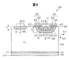
図6は、図2に示す実施形態のダイオード200と類似のダイオード600のさらに別の実施形態の一部分の断面を例示する。しかしながらダイオード600はゲート構造624の寸法によりダイオード200と異なる。図2のダイオード200のゲート構造224の一方の横方向広がりは第2のp型陽極領域206上で終わるが、図6のダイオード600のゲート構造624の対応する横方向の広がりはn型ドリフト領域602上で終わる。この特有の特徴は、電圧ブロッキング能力を有しない単極モードのダイオード600を動作させる際のn型ドリフト領域602内の電荷キャリア濃度のさらなる低減という技術的効果を与える。この単極モードでは、第1の側608においてn型ドリフト領域602とn型領域621間のチャネルに沿った電子流の流れを可能にするように正電圧がゲート電極628に印加される。したがってn型ドリフト領域602内の電荷キャリア濃度を低減しかつ非常に高速でダイオード600を動作させることが可能となる。しかしながら動作が逆回復を続ける前に、ダイオード600は電圧ブロッキング能力を有する動作モードに戻らなければならない(例えば、ゲート電極628に印加される電圧を変化させることにより)。
FIG. 6 illustrates a cross-section of a portion of yet another embodiment of a
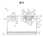
図7Aに、ダイオード700の別の実施形態の一部分の断面を例示する。ダイオード700は、第1のp型陽極領域704が、第1の側708から垂直方向710に沿ったn型ドリフト領域702内に延びるトレンチ分離部738に横方向に接するという点で図2に示すダイオード200と異なる。トレンチ分離部738は、例えばドライエッチング工程後にトレンチをシリコンの酸化物等の電気絶縁材により充填するなどのエッチング工程によりn型ドリフト領域702内にトレンチをエッチングすることにより形成されてもよい。図7Aの実施形態では、n型ドリフト領域702内において、トレンチ分離部738は第1のp型陽極領域704より深く延びる、すなわちトレンチ分離部738の底面は第1のp型陽極領域704の底面より下にある。他の実施形態によると、トレンチ分離部738の底面はまた、第1のp型陽極領域704の底面より上またはそれと同じレベルに位置してもよい。
FIG. 7A illustrates a cross section of a portion of another embodiment of a
ダイオード700はさらに、FET720が垂直チャネルトレンチFETであってFET220などの横方向チャネルFETではないという点で図2に示すダイオード200と異なる。FET720のゲート構造724はゲート電極728とトレンチ内に配置された誘電体726とを含む。ソースとドレインの一方を構成する第2のp型陽極領域706と、チャネル722を含むn型領域721と、ソースとドレインの他方を構成するp型領域730と、のそれぞれの側面はゲート構造724に接する。チャネル722の導電率はゲート電極728に印加された電圧により制御可能である。
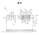
図7Bに、図7Aに示された実施形態のダイオード700と類似のダイオード700’のさらに別の実施形態の一部分の断面を例示する。
FIG. 7B illustrates a cross section of a portion of yet another embodiment of a diode 700 'similar to the
図7Bのダイオード700’は、n型ドリフト領域702内において、ゲート電極728’が第2のp型陽極領域706より深く延びる、すなわちゲート電極728’の底面は、第2のp型陽極領域706の底面より下に位置するという点で図7Aのダイオード700と異なる。換言すれば、第1の側708に対するゲート電極728’の底面の深さd5は第1の側708に対する第2のp型陽極領域706の底面の深さd6より大きい。
In the
図6に示す平面型FET620のゲート電極628と同様に、ゲート電極728’は、電圧ブロッキング能力を有しない単極モードのダイオード700’を動作させる際のn型ドリフト領域702内の電荷キャリア濃度のさらなる低減という技術的な効果を与える。この単極モードでは、トレンチの側壁におけるn型ドリフト領域702とn型領域721間の垂直チャネルに沿った電子流の流れを可能にするように正電圧がゲート電極728’に印加される。したがって、n型ドリフト領域702内の電荷キャリア濃度を低減しかつ非常に高速でダイオード700’を動作させることが可能となる。しかしながら動作が逆回復を続ける前に、ダイオード700’は電圧ブロッキング能力を有する動作モードに戻らなければならない(例えば、ゲート電極728’に印加される電圧を変化させることにより)。
Similar to the
図8Aに、図7Aに示された実施形態のダイオード700と同様なダイオード800の別の実施形態の一部分の断面を例示する。
FIG. 8A illustrates a cross-section of a portion of another embodiment of a
ダイオード800は、ダイオード800が第1のp型陽極領域804に接するトレンチ分離部を欠くという点で図7Aのダイオード700と異なる。その代り、第1のp型陽極領域804は、図2、4、6に示された実施形態と同様なn型ドリフト領域802により囲まれる。
The
図8Bは、図8Aに示された実施形態のダイオード800と同様なダイオード800’のさらに別の実施形態の一部分の断面を例示する。
FIG. 8B illustrates a cross-section of a portion of yet another embodiment of a diode 800 'similar to the
図8Bのダイオード800’は、n型ドリフト領域802内において、ゲート電極828’が第2のp型陽極領域806より深く延びる、すなわちゲート電極828’の底面は、第2のp型陽極領域806の底面より下に位置するという点で図8Aのダイオード800と異なる。換言すれば、第1の側808に対するゲート電極828’の底面の深さd5は第1の側808に対する第2のp型陽極領域806の底面の深さd6より大きい。ゲート電極828’の配置に関連する技術的効果に関しては、図7Bのゲート電極728’と上述の関連説明を参照されたい。
In the
他の実施形態によると、ダイオードは、横方向チャネルFETと、トレンチ絶縁部に横方向に接する第1のp型陽極領域と、を含んでよい。 According to another embodiment, the diode may include a lateral channel FET and a first p-type anode region that is in lateral contact with the trench insulator.
第1のp型陽極領域に隣接するトレンチ絶縁部の配置により、この領域のエミッタ効率を低減することができる。スイッチをトレンチFETとして形成すると、チャネル導電率を改善できるかもしれない。 By arranging the trench insulation adjacent to the first p-type anode region, the emitter efficiency of this region can be reduced. If the switch is formed as a trench FET, channel conductivity may be improved.
図9に、図2、4、6のダイオード200、400、600と類似の、陰極接触部916、n型陰極領域912、n型ドリフト領域902、第2のp型陽極領域906を含むダイオード900のさらに別の実施形態の一部分の断面を例示する。第1のp型陽極領域904、904’はマージドPINショットキーダイオードの一部である。マージドPINショットキーダイオードは、第1の側908上の金属接触部942とそれに接するn型ドリフト領域902間のショットキー接合をさらに含む。金属接触部942は、ダイオード900の第1の陽極接触部918の一部であってもよいし、あるいはそれに電気的に接続されてもよい。金属接触部942はまた、第1のp型陽極領域904、904’に対する電気的接続を与える。したがってマージドPINショットキーダイオードでは、第1のp型陽極領域904、904’と金属接触部942がこのマージドPINショットキーダイオードの陽極を構成する。
FIG. 9 illustrates a
スイッチSは、第2のp型陽極領域906と陽極接触部918間を電気的に接続または切断する。一実施形態によると、スイッチSはダイオード900の活性領域内に少なくとも部分的に形成されてもよい。別の実施形態によると、スイッチSはダイオード900の活性領域と異なる活性領域内に形成されてもよい。第2の陽極領域906とは異なり、マージドPINショットキーダイオードの陽極を、スイッチSにより作動化または非作動化することができない。マージドPINショットキーダイオードはエミッタ効率を低減させることができるので、開スイッチSと閉スイッチSの動作モード間のダイオード900の効率の差をさらに拡大させてもよい、すなわち、開スイッチSと閉スイッチSの動作モード間の電荷キャリア濃度の差をさらに拡大させてもよい。
The switch S electrically connects or disconnects between the second p-
他の実施形態によると、上記実施形態の半導体領域の導電型は逆であってもよい。したがって上述の陽極が陰極であり、上述の陰極が陽極であってもよい。この場合を図10に模式的に示す。図10に示す実施形態によると、ダイオード100’は陽極Aと陰極Cを含む。陰極Cは第1の陰極C1と第2の陰極C2を含む。第1の陰極C1は陰極接触部(図10に図示せず)に電気的に接続される。第2の陰極C2は、第2の陰極C2と陰極接触部間を電気的に接続または切断するように構成されたスイッチSを介し陰極接触部に電気的に接続される。
According to other embodiments, the conductivity types of the semiconductor regions of the above embodiments may be reversed. Therefore, the above-mentioned anode may be a cathode, and the above-mentioned cathode may be an anode. This case is schematically shown in FIG. According to the embodiment shown in FIG. 10, the
図2〜9に示された上記実施形態は、n型とp型だけでなく陽極と陰極も交換することにより、ダイオード100’に必要な変更を加える。 The above embodiments shown in FIGS. 2-9 make the necessary changes to the diode 100 'by replacing not only the n-type and p-type but also the anode and cathode.
「真下に」、「下に」、「下部の」、「上に」、「上部の」等の空間的相対用語は、1つの構成要素の第2の構成要素に対する位置の説明を簡単にするために使用される。これらの用語は、添付図面に図示したものとは異なる配向に加え装置の様々な配向を包含するように意図されている。さらに「第1」、「第2」等の用語はまた、様々な素子、領域、部分等を説明するために使用され、限定することを意図していない。同じ用語は本明細書を通し同じ構成要素を指す。 Spatial relative terms such as “below”, “below”, “bottom”, “above”, “top” simplify the description of the position of one component relative to the second component Used for. These terms are intended to encompass various orientations of the device in addition to orientations different from those illustrated in the accompanying drawings. Further, terms such as “first”, “second”, etc. are also used to describe various elements, regions, portions, etc., and are not intended to be limiting. The same terms refer to the same components throughout the specification.
本明細書で使用される際、用語「有する」、「含有する」、「含む」等は、明示された要素または特徴の存在を示すが追加要素または追加特徴を排除しない開放型用語である。単数形式の冠詞は文脈が明確に示さない限り単数だけでなく複数形式のものを含むように意図される。 As used herein, the terms “having”, “containing”, “including”, etc. are open terms that indicate the presence of an explicit element or feature but do not exclude additional elements or features. Articles in the singular are intended to include the plural as well as the singular unless the context clearly indicates otherwise.
本明細書に記載の様々な実施形態の特徴は特に明記しない限り互いに組み合わせられ得るということを理解すべきである。 It should be understood that the features of the various embodiments described herein may be combined with each other, unless expressly specified otherwise.
本明細書で使用される際、用語「電気的に接続」は構成要素同士が直接接続されなければならないことを意味するように意図されず、「電気的に接続」された構成要素間に介在構成要素が設けられてもよい。 As used herein, the term “electrically connected” is not intended to mean that the components must be directly connected to each other, but is interposed between “electrically connected” components. Components may be provided.
本明細書で使用される際、用語「活性領域」は、例えばトレンチ分離部または接合分離部等の絶縁により他の領域の半導体領域から電気的に絶縁された装置の半導体領域を指す。 As used herein, the term “active region” refers to a semiconductor region of a device that is electrically isolated from other regions of the semiconductor region by insulation, such as trench isolation or junction isolation.
本明細書で使用される際、特定の導電型(例えば、n型またはp型)の用語「不純物添加のドーズ量」は、例えば適切な方法(例えば、イオン注入)による単位表面積当たりの半導体本体(例えば、ドリフト領域)内に導入されるその特定の導電型のドーパントの数を指す。 As used herein, the term “impurity dose” for a particular conductivity type (eg, n-type or p-type) refers to a semiconductor body per unit surface area, eg, by a suitable method (eg, ion implantation). It refers to the number of dopants of that particular conductivity type that are introduced into (eg, drift region).
本明細書では特定の実施形態が例示され説明されたが、様々な代替のおよび/または等価な実施形態が本発明の範囲から逸脱することなく、上に示され説明された特定の実施形態を置換し得るということを当業者は理解することになる。本出願は、本明細書で検討された特定の実施形態のあらゆる適合化または変形を網羅するように意図されている。したがって本発明は特許請求の範囲とその等価物だけにより限定されるように意図されている。 While specific embodiments have been illustrated and described herein, various alternative and / or equivalent embodiments may be illustrated and described above without departing from the scope of the invention. Those skilled in the art will understand that substitutions can be made. This application is intended to cover any adaptations or variations of the specific embodiments discussed herein. Therefore, it is intended that this invention be limited only by the claims and the equivalents thereof.
100 ダイオード
A 陽極
A1 第1の陽極
A2 第2の陽極
C 陰極
S スイッチ
200、400、600、700、700’、800、800’、900 ダイオード
202、402、602、702、802、902 n型ドリフト領域
204、404、604、704、804、904、904’ 第1のp型陽極領域
206、406、606、706、806、906 第2のp型陽極領域
208、408、608、708、808 第1の側
210、410、610、710、810 垂直方向
211、411、611、711、811 横方向
212、412、612、712、812、912 n型陰極領域
214、414、614、714、814、914 第2の側
216、416、616、716、816、916 陰極接触部
218、418、618、718、818 陽極接触部
220、420、620、720、820 FET
221、421、621、721、821 n型領域
222、422、622、822 チャネル
224、424、624、724、824 ゲート構造
226、426、626、726、826 ゲート誘電体
228、428、628、728、728’、828、828’ ゲート電極
230、430、630、730、830 p型領域
434 第2のn型陰極領域
738 トレンチ分離部
918 陽極接触部
942 金属接触部
d1 第1のp型陽極領域の広がり
d2 第2のp型陽極領域の広がり
d5 ゲート電極’の底面の深さ
d6 第2のp型陽極領域の底面の深さ
N1、N2 p型不純物濃度
N3、N4 n型不純物濃度
A−A’、B−B、C−C’、D−D’ 断面線
100 Diode A Anode A 1 First anode A 2 Second anode C
221, 421, 621, 721, 821 n-
Claims (26)
第1のp型半導体陽極領域と第2のp型半導体陽極領域を含む陽極と、を含む半導体装置であって
前記第1のp型半導体陽極領域は陽極接触領域に電気的に接続され、
前記第2のp型半導体陽極領域は前記第2のp型半導体陽極領域と前記陽極接触領域間を電気的に接続または切断するように構成されたスイッチを介し前記陽極接触領域に電気的に接続される、半導体装置。 A cathode,
A semiconductor device including an anode including a first p-type semiconductor anode region and a second p-type semiconductor anode region, wherein the first p-type semiconductor anode region is electrically connected to an anode contact region,
The second p-type semiconductor anode region is electrically connected to the anode contact region via a switch configured to electrically connect or disconnect between the second p-type semiconductor anode region and the anode contact region. A semiconductor device.
前記第1の補助n型領域は前記第2のp型半導体陽極領域内に配置され、
前記第2の補助p型領域は前記第1の補助n型領域内に配置され、
前記第2のp型半導体陽極領域と前記第1の補助n型領域と前記第2の補助p型領域はそれぞれ半導体基板の表面に接し、
ゲートは前記第1の補助n型領域上に配置され、前記ゲートは前記第2の補助p型領域と前記第2のp型半導体陽極領域間の表面において前記第1の補助n型領域内に位置するチャネルの導電率を制御するように構成される、請求項12または13に記載の半導体装置。 The switch is a planar field effect transistor including a lateral channel;
The first auxiliary n-type region is disposed in the second p-type semiconductor anode region;
The second auxiliary p-type region is disposed in the first auxiliary n-type region;
The second p-type semiconductor anode region, the first auxiliary n-type region, and the second auxiliary p-type region are in contact with the surface of the semiconductor substrate, respectively.
A gate is disposed on the first auxiliary n-type region, and the gate is in the first auxiliary n-type region at a surface between the second auxiliary p-type region and the second p-type semiconductor anode region. 14. A semiconductor device according to claim 12 or 13, configured to control the conductivity of the located channel.
前記第1の補助n型領域は前記第2のp型半導体陽極領域内に配置され、
前記第2の補助p型領域は前記第1の補助n型領域内に配置され、
前記第1の補助n型領域と前記第2の補助p型領域は半導体基板の表面に接し、
ゲート電極はトレンチ内に配置され、前記ゲート電極は前記第2の補助p型領域と前記第2のp型半導体陽極領域間の前記トレンチの側壁における前記第1の補助n型領域内に位置するチャネルの導電率を制御するように構成される、請求項13に記載の半導体装置。 The switch is a trench field effect transistor including a vertical channel;
The first auxiliary n-type region is disposed in the second p-type semiconductor anode region;
The second auxiliary p-type region is disposed in the first auxiliary n-type region;
The first auxiliary n-type region and the second auxiliary p-type region are in contact with the surface of the semiconductor substrate;
A gate electrode is disposed in the trench, and the gate electrode is positioned in the first auxiliary n-type region on the sidewall of the trench between the second auxiliary p-type region and the second p-type semiconductor anode region. The semiconductor device of claim 13, configured to control the conductivity of the channel.
第1のn型半導体陰極領域と第2のn型半導体陰極領域を含む陰極とを含む半導体装置であって、
前記第1のn型半導体陰極領域は陰極接触領域に電気的に接続され、
前記第2のn型半導体陰極領域は、前記第2のn型半導体陰極領域と前記陰極接触領域間を電気的に接続または切断するように構成されたスイッチを介し前記陰極接触領域に電気的に接続される、半導体装置。 The anode,
A semiconductor device including a first n-type semiconductor cathode region and a cathode including a second n-type semiconductor cathode region,
The first n-type semiconductor cathode region is electrically connected to a cathode contact region;
The second n-type semiconductor cathode region is electrically connected to the cathode contact region via a switch configured to electrically connect or disconnect between the second n-type semiconductor cathode region and the cathode contact region. A semiconductor device to be connected.
Applications Claiming Priority (2)
| Application Number | Priority Date | Filing Date | Title |
|---|---|---|---|
| US12/980,041 US8415747B2 (en) | 2010-12-28 | 2010-12-28 | Semiconductor device including diode |
| US12/980,041 | 2010-12-28 |
Publications (2)
| Publication Number | Publication Date |
|---|---|
| JP2012146977A true JP2012146977A (en) | 2012-08-02 |
| JP5872281B2 JP5872281B2 (en) | 2016-03-01 |
Family
ID=46315597
Family Applications (1)
| Application Number | Title | Priority Date | Filing Date |
|---|---|---|---|
| JP2011282710A Active JP5872281B2 (en) | 2010-12-28 | 2011-12-26 | Semiconductor device including a diode |
Country Status (4)
| Country | Link |
|---|---|
| US (1) | US8415747B2 (en) |
| JP (1) | JP5872281B2 (en) |
| CN (1) | CN102569298B (en) |
| DE (1) | DE102011056956A1 (en) |
Cited By (4)
| Publication number | Priority date | Publication date | Assignee | Title |
|---|---|---|---|---|
| JP2017135175A (en) * | 2016-01-26 | 2017-08-03 | 豊田合成株式会社 | Semiconductor device, power conversion device, and method for manufacturing semiconductor device |
| WO2018135224A1 (en) | 2017-01-18 | 2018-07-26 | 株式会社日立パワーデバイス | Semiconductor device and electric power conversion device using same |
| WO2021112076A1 (en) * | 2019-12-06 | 2021-06-10 | 株式会社日立製作所 | Semiconductor circuit control method, and power converter adopting same |
| DE112022001954T5 (en) | 2021-09-02 | 2024-01-18 | Hitachi Power Semiconductor Device, Ltd. | SEMICONDUCTOR DEVICE, METHOD FOR PRODUCING THE SEMICONDUCTOR DEVICE AND POWER CONVERSION DEVICE |
Families Citing this family (7)
| Publication number | Priority date | Publication date | Assignee | Title |
|---|---|---|---|---|
| DE102015102138B4 (en) * | 2015-02-13 | 2017-02-02 | Infineon Technologies Ag | Semiconductor devices and a method of forming a semiconductor device |
| DE102015120210B4 (en) * | 2015-11-23 | 2019-02-21 | Infineon Technologies Ag | Power semiconductor transistor with increased bipolar gain |
| DE102016105699B4 (en) * | 2016-03-29 | 2019-12-12 | Infineon Technologies Ag | A semiconductor device having fin portions between gate structures extending into a semiconductor portion |
| DE102016112490B4 (en) | 2016-07-07 | 2022-05-25 | Infineon Technologies Ag | Semiconductor devices and method of forming a semiconductor device |
| TWI630700B (en) * | 2017-05-10 | 2018-07-21 | 新唐科技股份有限公司 | Semiconductor device |
| JP6896672B2 (en) * | 2018-03-21 | 2021-06-30 | 株式会社東芝 | Semiconductor devices and their manufacturing methods |
| GB2609343B (en) * | 2018-07-23 | 2023-06-07 | Ween Semiconductors Co Ltd | Power Semiconductor Device |
Citations (13)
| Publication number | Priority date | Publication date | Assignee | Title |
|---|---|---|---|---|
| JPS63107169A (en) * | 1986-10-24 | 1988-05-12 | Fuji Electric Co Ltd | Reverse conducting gto thyristor |
| JPH02126669A (en) * | 1988-08-31 | 1990-05-15 | Sgs Thomson Microelectron Sa | Composite mos transistor and free ring diode |
| JPH0677506A (en) * | 1992-04-17 | 1994-03-18 | Fuji Electric Co Ltd | Semiconductor device and its driving method |
| JPH07263640A (en) * | 1994-03-04 | 1995-10-13 | Siemens Ag | Semiconductor device for overvoltage protection |
| JPH07302904A (en) * | 1994-05-05 | 1995-11-14 | Fuji Electric Co Ltd | Semiconductor device and its control method |
| JPH0832064A (en) * | 1994-07-15 | 1996-02-02 | Fuji Electric Co Ltd | Mos semiconductor device, drive method and circuit thereof |
| JPH08293618A (en) * | 1995-04-20 | 1996-11-05 | Toshiba Corp | High breakdown strength semiconductor device |
| JPH09107097A (en) * | 1995-10-11 | 1997-04-22 | Fuji Electric Co Ltd | Rectifier device and its drive method |
| JP2002076343A (en) * | 2000-08-23 | 2002-03-15 | Toshiba Corp | Semiconductor device |
| JP2003509836A (en) * | 1999-05-25 | 2003-03-11 | ウィリアムス、リチャード・ケイ | Trench semiconductor device with gate oxide layer having multiple thicknesses and method of manufacturing the same |
| JP2007311822A (en) * | 2007-07-23 | 2007-11-29 | Toshiba Corp | Schottky barrier diode |
| JP2008539571A (en) * | 2005-04-28 | 2008-11-13 | シーメンス アクチエンゲゼルシヤフト | Controllable semiconductor diodes, electronic components and intermediate voltage converters |
| JP2010062377A (en) * | 2008-09-04 | 2010-03-18 | Sanyo Electric Co Ltd | Semiconductor device and manufacturing method thereof |
Family Cites Families (2)
| Publication number | Priority date | Publication date | Assignee | Title |
|---|---|---|---|---|
| US6642088B1 (en) * | 2002-04-10 | 2003-11-04 | Taiwan Semiconductor Manufacturing Company | Silicon-controlled rectifier structures on silicon-on insulator with shallow trench isolation |
| US8389352B2 (en) * | 2011-02-11 | 2013-03-05 | International Business Machines Corporation | Silicon germanium film formation method and structure |
-
2010
- 2010-12-28 US US12/980,041 patent/US8415747B2/en active Active
-
2011
- 2011-12-23 DE DE102011056956A patent/DE102011056956A1/en active Pending
- 2011-12-26 JP JP2011282710A patent/JP5872281B2/en active Active
- 2011-12-28 CN CN201110446266.5A patent/CN102569298B/en active Active
Patent Citations (13)
| Publication number | Priority date | Publication date | Assignee | Title |
|---|---|---|---|---|
| JPS63107169A (en) * | 1986-10-24 | 1988-05-12 | Fuji Electric Co Ltd | Reverse conducting gto thyristor |
| JPH02126669A (en) * | 1988-08-31 | 1990-05-15 | Sgs Thomson Microelectron Sa | Composite mos transistor and free ring diode |
| JPH0677506A (en) * | 1992-04-17 | 1994-03-18 | Fuji Electric Co Ltd | Semiconductor device and its driving method |
| JPH07263640A (en) * | 1994-03-04 | 1995-10-13 | Siemens Ag | Semiconductor device for overvoltage protection |
| JPH07302904A (en) * | 1994-05-05 | 1995-11-14 | Fuji Electric Co Ltd | Semiconductor device and its control method |
| JPH0832064A (en) * | 1994-07-15 | 1996-02-02 | Fuji Electric Co Ltd | Mos semiconductor device, drive method and circuit thereof |
| JPH08293618A (en) * | 1995-04-20 | 1996-11-05 | Toshiba Corp | High breakdown strength semiconductor device |
| JPH09107097A (en) * | 1995-10-11 | 1997-04-22 | Fuji Electric Co Ltd | Rectifier device and its drive method |
| JP2003509836A (en) * | 1999-05-25 | 2003-03-11 | ウィリアムス、リチャード・ケイ | Trench semiconductor device with gate oxide layer having multiple thicknesses and method of manufacturing the same |
| JP2002076343A (en) * | 2000-08-23 | 2002-03-15 | Toshiba Corp | Semiconductor device |
| JP2008539571A (en) * | 2005-04-28 | 2008-11-13 | シーメンス アクチエンゲゼルシヤフト | Controllable semiconductor diodes, electronic components and intermediate voltage converters |
| JP2007311822A (en) * | 2007-07-23 | 2007-11-29 | Toshiba Corp | Schottky barrier diode |
| JP2010062377A (en) * | 2008-09-04 | 2010-03-18 | Sanyo Electric Co Ltd | Semiconductor device and manufacturing method thereof |
Cited By (7)
| Publication number | Priority date | Publication date | Assignee | Title |
|---|---|---|---|---|
| JP2017135175A (en) * | 2016-01-26 | 2017-08-03 | 豊田合成株式会社 | Semiconductor device, power conversion device, and method for manufacturing semiconductor device |
| WO2018135224A1 (en) | 2017-01-18 | 2018-07-26 | 株式会社日立パワーデバイス | Semiconductor device and electric power conversion device using same |
| JP2018117044A (en) * | 2017-01-18 | 2018-07-26 | 株式会社 日立パワーデバイス | Semiconductor device and power conversion device using the same |
| WO2021112076A1 (en) * | 2019-12-06 | 2021-06-10 | 株式会社日立製作所 | Semiconductor circuit control method, and power converter adopting same |
| JP2021090026A (en) * | 2019-12-06 | 2021-06-10 | 株式会社日立製作所 | Semiconductor circuit control method and power converter using the method |
| JP7315443B2 (en) | 2019-12-06 | 2023-07-26 | 株式会社日立製作所 | SEMICONDUCTOR CIRCUIT CONTROL METHOD AND POWER CONVERTER USING THE SAME |
| DE112022001954T5 (en) | 2021-09-02 | 2024-01-18 | Hitachi Power Semiconductor Device, Ltd. | SEMICONDUCTOR DEVICE, METHOD FOR PRODUCING THE SEMICONDUCTOR DEVICE AND POWER CONVERSION DEVICE |
Also Published As
| Publication number | Publication date |
|---|---|
| JP5872281B2 (en) | 2016-03-01 |
| US8415747B2 (en) | 2013-04-09 |
| CN102569298A (en) | 2012-07-11 |
| US20120161224A1 (en) | 2012-06-28 |
| DE102011056956A1 (en) | 2012-06-28 |
| CN102569298B (en) | 2015-06-17 |
Similar Documents
| Publication | Publication Date | Title |
|---|---|---|
| JP5872281B2 (en) | Semiconductor device including a diode | |
| US8778764B2 (en) | Method of making an insulated gate semiconductor device having a shield electrode structure and structure therefor | |
| CN108257953B (en) | Semiconductor device having IGBT region and non-switchable diode region | |
| US10680089B2 (en) | Semiconductor device having an active trench and a body trench | |
| CN107026207B (en) | Semiconductor device including lateral transistor | |
| JP2005510059A (en) | Field effect transistor semiconductor device | |
| US10490658B2 (en) | Power semiconductor device | |
| WO2007117307A2 (en) | Trench field plate termination for power devices | |
| KR101896332B1 (en) | Semiconductor device and method manufacturing the same | |
| US7989921B2 (en) | Soi vertical bipolar power component | |
| US20230343863A1 (en) | Semiconductor Device Including First Gate Electrode and Second Gate Electrode | |
| US20110156093A1 (en) | High-voltage power transistor using soi technology | |
| CN112670340B (en) | P-type grid HEMT device | |
| US11094691B2 (en) | Semiconductor device | |
| CN113675265A (en) | Vertical power semiconductor device and method of manufacture | |
| CN113053991A (en) | Cell structure of reverse conducting IGBT and reverse conducting IGBT | |
| TWI794647B (en) | Device of improving igbt light load efficiency | |
| US20240072178A1 (en) | Diode and manufacturing method therefor, and semiconductor device | |
| CN107768240B (en) | Source region structure of trench transistor and preparation method thereof | |
| CN112909084A (en) | Semiconductor device including insulated gate bipolar transistor | |
| CN117099209A (en) | Power semiconductor device and method for manufacturing the same | |
| CN114586174A (en) | Vertical field effect transistor and method for its construction | |
| TW201526203A (en) | Semiconductor device and method of fabricating the same | |
| CN113632237A (en) | Reverse conducting insulated gate power semiconductor device with low conduction loss | |
| US20160013268A1 (en) | Power semiconductor device |
Legal Events
| Date | Code | Title | Description |
|---|---|---|---|
| A977 | Report on retrieval |
Free format text: JAPANESE INTERMEDIATE CODE: A971007 Effective date: 20131028 |
|
| A601 | Written request for extension of time |
Free format text: JAPANESE INTERMEDIATE CODE: A601 Effective date: 20140204 |
|
| A602 | Written permission of extension of time |
Free format text: JAPANESE INTERMEDIATE CODE: A602 Effective date: 20140207 |
|
| A521 | Request for written amendment filed |
Free format text: JAPANESE INTERMEDIATE CODE: A523 Effective date: 20140217 |
|
| A131 | Notification of reasons for refusal |
Free format text: JAPANESE INTERMEDIATE CODE: A131 Effective date: 20140708 |
|
| A521 | Request for written amendment filed |
Free format text: JAPANESE INTERMEDIATE CODE: A523 Effective date: 20140916 |
|
| A02 | Decision of refusal |
Free format text: JAPANESE INTERMEDIATE CODE: A02 Effective date: 20150210 |
|
| A521 | Request for written amendment filed |
Free format text: JAPANESE INTERMEDIATE CODE: A523 Effective date: 20150608 |
|
| A911 | Transfer to examiner for re-examination before appeal (zenchi) |
Free format text: JAPANESE INTERMEDIATE CODE: A911 Effective date: 20150805 |
|
| A131 | Notification of reasons for refusal |
Free format text: JAPANESE INTERMEDIATE CODE: A131 Effective date: 20150929 |
|
| A521 | Request for written amendment filed |
Free format text: JAPANESE INTERMEDIATE CODE: A523 Effective date: 20151125 |
|
| TRDD | Decision of grant or rejection written | ||
| A01 | Written decision to grant a patent or to grant a registration (utility model) |
Free format text: JAPANESE INTERMEDIATE CODE: A01 Effective date: 20151215 |
|
| A61 | First payment of annual fees (during grant procedure) |
Free format text: JAPANESE INTERMEDIATE CODE: A61 Effective date: 20160113 |
|
| R150 | Certificate of patent or registration of utility model |
Ref document number: 5872281 Country of ref document: JP Free format text: JAPANESE INTERMEDIATE CODE: R150 |
|
| R250 | Receipt of annual fees |
Free format text: JAPANESE INTERMEDIATE CODE: R250 |
|
| R250 | Receipt of annual fees |
Free format text: JAPANESE INTERMEDIATE CODE: R250 |
|
| R250 | Receipt of annual fees |
Free format text: JAPANESE INTERMEDIATE CODE: R250 |
|
| R250 | Receipt of annual fees |
Free format text: JAPANESE INTERMEDIATE CODE: R250 |
|
| R250 | Receipt of annual fees |
Free format text: JAPANESE INTERMEDIATE CODE: R250 |
|
| R250 | Receipt of annual fees |
Free format text: JAPANESE INTERMEDIATE CODE: R250 |