JP2012146940A - Electronic component and electronic device - Google Patents
Electronic component and electronic device Download PDFInfo
- Publication number
- JP2012146940A JP2012146940A JP2011043968A JP2011043968A JP2012146940A JP 2012146940 A JP2012146940 A JP 2012146940A JP 2011043968 A JP2011043968 A JP 2011043968A JP 2011043968 A JP2011043968 A JP 2011043968A JP 2012146940 A JP2012146940 A JP 2012146940A
- Authority
- JP
- Japan
- Prior art keywords
- external connection
- circuit pattern
- electronic component
- connection terminal
- laminate
- Prior art date
- Legal status (The legal status is an assumption and is not a legal conclusion. Google has not performed a legal analysis and makes no representation as to the accuracy of the status listed.)
- Withdrawn
Links
Images


Abstract
Description
本発明は、電子部品および電子装置に関するものである。 The present invention relates to an electronic component and an electronic device.
ノイズを減衰させるフィルタとして、例えば、複数の絶縁体層が積層された積層体と、積層体の積層方向に沿った四側面にそれぞれ設けられた複数の共通端子と、複数の共通端子と電気的に接続され、絶縁体層間に設けられた回路パターンとを備えた電子部品が提案されている(例えば、特許文献1を参照。)。 As a filter for attenuating noise, for example, a laminated body in which a plurality of insulator layers are laminated, a plurality of common terminals provided on four side surfaces along the lamination direction of the laminated body, a plurality of common terminals, And an electronic component including a circuit pattern provided between insulator layers has been proposed (see, for example, Patent Document 1).
このようなフィルタ部品は積層体の積層方向と垂直な主面を実装面として、配線基板の一主面に実装される。各共通端子は積層体の実装面に設けられており、この実装面を配線基板の一主面に対向させ、共通端子と配線基板の一主面に設けられている複数のランドとを半田接合することによって、フィルタ部品が配線基板上に実装される。 Such a filter component is mounted on one main surface of the wiring board with a main surface perpendicular to the stacking direction of the laminate as a mounting surface. Each common terminal is provided on the mounting surface of the laminate. The mounting surface is opposed to one main surface of the wiring board, and the common terminals and a plurality of lands provided on the one main surface of the wiring board are soldered together. By doing so, the filter component is mounted on the wiring board.
しかしながら、上述した従来の実装構造体においては積層体内の回路パターンと配線基板のランドとが広い面積で対向することに起因して、両者間で大きな容量が発生してしまい、所望する電気的特性が得られなくなる場合がある。 However, in the conventional mounting structure described above, a large capacitance is generated between the circuit pattern in the laminate and the land of the wiring board facing each other over a wide area, and desired electrical characteristics are obtained. May not be obtained.
本発明は、以上のような問題点に鑑みて案出されたものであり、その目的は、電子部品を配線基板に実装した際に、不要な容量が発生するのを抑制することが可能な電子部品を提供することにある。 The present invention has been devised in view of the above problems, and an object of the present invention is to suppress generation of unnecessary capacitance when an electronic component is mounted on a wiring board. To provide electronic components.
本発明の電子部品は、複数の絶縁体層が積層された直方体状の積層体と、該積層体の積層方向に沿った四側面のうち一側面に設けられた外部接続端子と、該外部接続端子と電気的に接続され、前記絶縁体層間に設けられた回路パターンとを備えているものである。 The electronic component of the present invention includes a rectangular parallelepiped laminate in which a plurality of insulator layers are laminated, an external connection terminal provided on one side surface among four sides along the lamination direction of the laminate, and the external connection A circuit pattern electrically connected to the terminal and provided between the insulator layers.
本発明の電子装置は、上記の電子部品と、一主面に前記外部接続端子と対応する複数のランドを有する配線基板とを有しており、前記電子部品が、前記一側面の前記外部接続端子を前記複数のランドに対向させた状態で前記配線基板の前記一主面上に実装されていることを特徴とするものである。 The electronic device of the present invention includes the above-described electronic component and a wiring board having a plurality of lands corresponding to the external connection terminals on one main surface, and the electronic component is the external connection on the one side surface. The terminal is mounted on the one main surface of the wiring board in a state of facing the plurality of lands.
本発明の電子部品によれば、複数の絶縁体層が積層された直方体状の積層体と、積層体の積層方向に沿った四側面のうち一側面に設けられた外部接続端子と、外部接続端子と電気的に接続され、絶縁体層間に設けられた回路パターンとを備えていることから、外部接続端子を配線基板の複数のランドに接続する際、外部接続端子が設けられている積層体の一側面を実装面として用いることにより、配線基板のランドに対して回路パターンが対向する面積を小さくすることができる。その結果、回路パターンと複数のランド間で不要な容量が発生するのを抑制できる。 According to the electronic component of the present invention, a rectangular parallelepiped laminate in which a plurality of insulator layers are laminated, an external connection terminal provided on one side surface among four side surfaces along the lamination direction of the laminate, and an external connection Since it has a circuit pattern electrically connected to the terminals and provided between the insulator layers, when the external connection terminals are connected to a plurality of lands on the wiring board, the laminated body provided with the external connection terminals By using one side surface as the mounting surface, the area of the circuit pattern facing the land of the wiring board can be reduced. As a result, generation of unnecessary capacitance between the circuit pattern and the plurality of lands can be suppressed.
以下に、本発明の電子部品の実施の形態の一例について図面を参照しつつ詳細に説明する。 Hereinafter, an example of an embodiment of an electronic component of the present invention will be described in detail with reference to the drawings.
図1および図3に示すように、電子部品1は、積層体2と、外部接続端子3と、電子回路4とを備えている。
As shown in FIGS. 1 and 3, the
電子部品1は、例えば、携帯電話または小型PC(Personal Computer)等の移動体通
信機器内部における、LCD,メモリー部,RF回路およびカメラ部等の各構成部への信号を伝送するための信号ライン等で用いられる。この信号ラインには外部からのノイズが混入しやすいので、電子部品1は、このノイズを減衰させるノイズフィルタ素子として使用される。また、電子部品1は、携帯電話または小型PC等の他に、例えば、カーナビゲーションシステムやテレビ等の、一般的に高周波信号が使用されるデジタル機器にも使用される。
The
積層体2は、複数の絶縁体層5が積層されて成り、直方体状である。この積層体2は、1層当たり例えば5μm〜300μmの厚みに形成された矩形状の複数の絶縁体層5を、例
えば2〜50層積層して成る直方体状の絶電体ブロックである。
The
また、積層体2の寸法は、積層体2の長辺の長さを、例えば1〜3mmとし、積層体2の短辺の長さを、例えば0.5〜2mmとし、積層体2の高さを、例えば0.3〜2mmとする。
The dimensions of the
絶縁体層5の材料としては、例えば、誘電体セラミック材料が用いられ、必要に応じて焼結助剤、低融点ガラス材料等を用いても良い。誘電体セラミック材料としては、例えばTiO2−Nd2O3−BaTiO3系等セラミック材料が用いられる。焼結助剤としては、例えば、BiVO4、CuO、Li2O、B2O3等が用いられる。
As a material of the
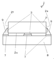
積層体2は、図1に示すように、互いに対向する第1の主面2a及び第2の主面2bと、互いに対向する第1の側面2c及び第2の側面2dと、互いに対向する第3の側面2e及び第4の側面2fとを有する略直方体状に形成されている。
As shown in FIG. 1, the
回路パターン6は、外部接続端子3と電気的に接続され、絶縁体層5間に設けられている。この回路パターン6は、コンデンサおよびインダクタの少なくとも一部を構成することにより、電子回路4を形成する。
The
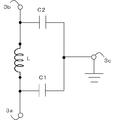
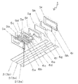
図3に示す例においては、絶縁体層5a〜5iが積層されて積層体2となっている。これら絶縁体層5間に回路パターン6が形成されることにより、電子回路4としてフィルタ回路が形成されている。図3に示す例において、このフィルタ回路において、絶縁体層5a〜5f上の回路パターン6a〜6fは、絶縁体層5a〜5eを貫通するビアホール導体によって、互いに接続されて所定の巻き数を有するコイル状のインダクタ素子L1を構成している。また、絶縁体層5h、5i上の回路パターン6h、6iは第1コンデンサ素子C1を構成している。また、絶縁体層5g、5h上の回路パターン6g、6hは第2コンデンサ素子C2を構成している。
In the example illustrated in FIG. 3, the
絶縁体層5a、5i上の回路パターン6a、6iは入力端子3aに接続されている。絶縁体層5f、5g上の回路パターン6f、6gは出力端子3bに接続されている。絶縁体層5h上の回路パターン6hはグランド端子3cに接続されている。
The
なお、図3では、絶縁体層5a〜5iを9層用いて積層体2を形成した例を示したが、絶縁体層5a上に、回路パターン6aを覆うようにさらに1又は複数の絶縁体層5を配置させても良い。また、絶縁体層5iの回路パターン6iが形成されていない面に、さらに1又は複数の絶縁体層5が配置されていてもよい。
FIG. 3 shows an example in which the
以上の構成の電子回路4は、図4に示すような、両端が一対の入出力端子3a、3bにそれぞれ接続されたインダクタ素子Lと、入力端子3aおよび接地端子3cの間に配置された第1コンデンサ素子C1と、入力端子3bおよび接地端子3cの間に配置された第2コンデンサ素子C2とから成る等価回路として表される。
As shown in FIG. 4, the electronic circuit 4 having the above configuration includes an inductor element L whose both ends are connected to a pair of input /
絶縁体層5a〜5iに形成される回路パターン6a〜6iの材料としては、AgまたはAg−Pd合金もしくはAg−Pt合金等のAgを主成分とする合金などから成る導電材料、あるいはCuまたはCu−Zn合金,Cu−Sn合金,Cu−Ag合金もしくはCu−Ni合金等のCuを主成分とする合金などから成る導電材料を用いることができ、各種電極の厚みは、例えば5μm〜25μmに適宜設定される。
As the material of the
外部接続端子3は、図1に示す例では、積層体2の積層方向に沿った四側面のうち一側面2c(第1の側面2c)に設けられている。なお、図1に示す例において積層体2の第1の側面2cに設けられた外部接続端子3は、それぞれ入力端子3a、出力端子3b、グランド端子3cとして機能する。
In the example illustrated in FIG. 1, the
図1に示す例では、外部接続端子3は、積層体2の積層方向に沿って帯状に設けられている。この外部接続端子3は、例えば長さが0.3〜2mmであり、幅が0.2mm〜0.3mm
である。また、外部接続端子3の厚みは、例えば10μm〜25μmである。
In the example shown in FIG. 1, the
It is. The thickness of the
また、これら外部接続端子3の形状は、第1の側面2cにおいて、積層体2の積層方向に対して斜めである帯状または楕円形状等であってもよいものである。外部接続端子3は、スクリーン印刷又は金属箔の転写等の方法によって形成される。
Further, the shape of these
以上の構成の電子部品1は、図2および図3に示すように、一主面に外部接続端子3と対応する複数のランド7a〜7cを有する配線基板8に実装される。そして、電子部品1は、一側面(第1の側面2c)の複数の外部接続端子3を複数のランド7a〜7cに対向させた状態で配線基板8の一主面上に実装される。
As shown in FIGS. 2 and 3, the
電子部品1の実装面は、図2に示すように、第1の側面2cである。このように、電子部品1は、外部接続端子3が第1の側面2cに設けられているので、この側面2cを実装面とできる。
As shown in FIG. 2, the mounting surface of the
このような構成により、配線基板8のランド7に対して回路パターン6が対向する面積を小さくすることができる。その結果、回路パターン6と複数のランド7間で不要な容量が発生するのを抑制できる。
With such a configuration, the area of the
配線基板8の材料としては、例えば、酸化アルミニウム質焼結体、窒化アルミニウム質焼結体、ムライト質焼結体、炭化珪素質焼結体、ガラスセラミックス焼結体等のセラミック材料が用いられる。また、ポリイミド樹脂、エポキシ樹脂等の有機樹脂材料を用いてもよい。また、セラミックスまたはガラス等の無機材料をエポキシ樹脂等の有機樹脂材料に混合させて成る複合材等を用いてもよい。
As the material of the
ランド7は、外部接続端子3と対応するように、配線基板8の一主面に設けられている。このランド7は、W、Cu、Ag、Au、Pd、Ta、Mn等の金属材料により形成される。このランド7の形成手段としては、メタライズ層、めっき層、蒸着等による金属の薄膜層として外部接続端子3を積層体2に被着させる手段を用いることができる。例えば、W及びAgから成るペーストを配線基板8の一主面となるグリーンシートにメタライズ層として印刷してこれをグリーンシートとともに焼成する方法が用いられる。また、金属箔を転写することによって、ランド7を形成してもよい。
The
ランド7および接続端子3は、接合材(図示せず。)を介して電気的に接続される。この接合材は、Sn−Ag系またはSn−Ag−Cu系等の半田、Au−Sn等の低融点ろう材、Ag−Ge系等の高融点ろう材、導電性有機樹脂、あるいはシーム溶接・電子ビーム溶接等の溶接法による接合を可能とするような金属材料等により形成されている。
The
また、本例の電子部品1によれば、コンデンサを構成するような面積の広い回路パターン6を、積層方向のどこに位置させたとしても、配線基板8のランド7と回路パターン6との間での不要な容量発生を抑制することができる。よって、電子部品1内の回路を設計する際に、回路パターン6の配置の自由度を向上させることができるので好ましい。
Further, according to the
また、外部接続端子3が設けられた一側面は、四側面2c〜2fのうちの短辺を有する側面2e(2f)であることが好ましい。この構成により、この短辺を有する側面2e(2f)を配線基板に対する実装面とすることができる。よって、回路パターン6の短手方向を配線基板8側にすることができる。従って、図5に示すように、回路パターン6の厚み幅と配線基板8のランド7との対向領域をさらに減少させることができる。結果、ランド7と回路パターン6との間における不要な容量の発生をさらに抑制させることができる。
Moreover, it is preferable that the one side surface provided with the
また、図3に示す例の回路パターン6の、外部接続端子3の配列方向の長さは、外部接続端子1つ分の幅以下であることが好ましい。これによって、回路パターン6の厚み幅と、ランド7との対向領域の面積をさらに軽減することができる。よって、ランド7と回路パターン6との間における不要な容量の発生をさらに抑制させることができる。
Moreover, it is preferable that the length of the
例えば、外部接続端子3の幅は、積層体2の外表面に引き出されている部分の回路パターン6の幅と略同一であることが好ましい。略同一とは、外部接続端子3の幅と回路パターン6の引き出し部の幅との差が、外部接続端子3の幅の5%以内ということである。外部接続端子3の幅を、回路パターン6の幅と比較して大きすぎないように制御することで
、外部接続端子3と回路パターン6の厚み幅との対向領域の面積が増大することを抑制できる。よって、外部接続端子3と回路パターンとの間における不要な容量発生を抑制させることができる。
For example, it is preferable that the width of the
また、図3に示す例においては、外部接続端子3は積層方向に沿って延びるように設けられている。このような構成によって、外部接続端子3は、積層方向の面積を広くできる。よって、ランド7と接続する際に位置ずれによる電気的接続不良を防ぐことができる。
In the example shown in FIG. 3, the
また、例えば、外部接続端子3は積層方向に部分的に形成することが好ましい。このような構成によって、他の回路パターンの厚み幅との間で、不要な容量の発生を抑制できる。
For example, it is preferable to form the
なお、このときの配線基板8の複数のランド7は、積層体2の積層方向に沿って延びていることが好ましい。この構成によれば、前述したように積層方向に延びている外部接続端子3とランド7との接触面積を増大できる。よって、両者間の電気抵抗を軽減することができる。
At this time, the plurality of
電子部品1は、以下に示すようなセラミックグリーンシート積層法によって作製される。
The
具体的には、まず、例えばTiO2−Nd2O3−BaTiO3から成る誘電体セラミック材料粉末に適当な有機溶剤等を添加し混合して泥漿状にするとともに、ドクターブレード法等を用いることによってセラミックグリーンシートを形成する。 Specifically, first, an appropriate organic solvent or the like is added to and mixed with a dielectric ceramic material powder made of, for example, TiO 2 —Nd 2 O 3 —BaTiO 3 to form a slurry, and a doctor blade method or the like is used. To form a ceramic green sheet.
次に、得られたセラミックグリーンシートにスクリーン印刷法等によって、各種回路パターン6a〜6iを形成して、これらを積層し圧着して積層体2の成形体を形成する。
Next,
次に、この積層体2の成形体を所定の大きさに分割して、800〜1050℃で焼成すること
により焼結した積層体2が得られる。
Next, the
次に、得られた積層体2の角部に、マイクロクラックの除去および欠けの発生を防止する目的で、バレル研磨等による面取りを施す。
Next, chamfering by barrel polishing or the like is performed on the corners of the obtained
次に、面取りが施された積層体2の表面に、Ag,Ag−Pd合金またはAg−Pt合金等から成る導電材料から成るグランド端子3cおよび入出力端子3a、3bを形成する。このとき、グランド端子3cおよび入出力端子3a、3bとなる導体ペーストを、積層体2の表面にスクリーン印刷法等によって所定パターンに塗布する。次に、導体ペーストが塗布された積層体2を焼成して、グランド端子3cおよび入出力端子3a、3bを形成する。そして、グランド端子3cおよび入出力端子3a、3bの表面に、必要に応じてNiメッキ層,Auメッキ層,Snメッキ層または半田メッキ層等のメッキ層を形成して、電子部品1を得る。
Next, the
なお、本発明は上述した実施の形態の例に限定されるものではなく、本発明の要旨を逸脱しない範囲において種々の変更,改良等が可能である。 The present invention is not limited to the embodiments described above, and various changes and improvements can be made without departing from the scope of the present invention.
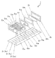
例えば、図6に示すように、外部接続端子3を、積層体2の一側面(2c)に設け、他の外部接続端子3を一側面(2c)に隣接する側面(2f、2e)に設けるとともに、他の外部接続端子3と電気的に接続されるランド7は、平面視で積層体2と重ならないように配置されていることが好ましい。
For example, as shown in FIG. 6, the
このような構成によって、他の外部接続端子3と接続されるランド7は、積層体2内の回路パターン6の厚み幅と対向しなくなるので、不要な容量の発生をさらに抑制させることができる。
With such a configuration, the
なお、図6に示す例においては、他の外部接続端子3とランド7とは、前述したのと同様の材料から成る接合材9を介して接続されている。
In the example shown in FIG. 6, the other
図7と図13とは、ともに図8に示した等価回路を構成する。図9と図14とは、ともに図10に示した等価回路を構成する。図11と図15とは、ともに図12に示した等価回路を構成する。 7 and 13 together constitute the equivalent circuit shown in FIG. 9 and 14 together constitute the equivalent circuit shown in FIG. 11 and 15 together constitute the equivalent circuit shown in FIG.
このように、図7、図9、図11に示す例の電子部品と、図13〜図15に示す例の従来の電子部品とは、等価回路は同じであるが、外部接続端子3が積層体2の一側面2cに設けられている点が異なる。これによって、上述したように、配線基板8のランド7に対して回路パターン6が対向する面積を小さくすることができる。その結果、回路パターン6と複数のランド7間で不要な容量が発生するのを抑制できる。さらに、図7、図9、図11に示す例においては、外部接続端子3と、回路パターン6とが、ビアホール導体を介することなく電気的に接続されている構成となる。よって、積層体2中に存在するビアホール導体は、異なる絶縁体層5間の回路パターン6同士を接続するものに限られる。他方、図13〜図15に示す例においては、外部接続端子3が積層体2の主面に設けられているので、外部接続端子3と、回路パターン6とが、ビアホール導体を介して接続されている。結果、図7、図9、図11に示す例の構成によれば、図13〜図15と比較して、積層体2中において外部接続端子3と回路パターン6とを接続するビアホール導体の分だけ、ビアホール導体の全体の数を減少させることができる。
As described above, the electronic components in the examples shown in FIGS. 7, 9, and 11 and the conventional electronic components in the examples shown in FIGS. 13 to 15 have the same equivalent circuit, but the
例えば、図13〜図15においては、回路パターン6aと外部接続端子3aとを接続するために、絶縁体層5a〜5iを貫通するビアホール導体を設けているが、図7、図9、
図11に示す例の構成によれば、回路パターン6aを外部接続端子3aに直接接続させているので、その分ビアホール導体を省略している。よって、図13〜図15と比較して、積層体2中のビアホール導体の数を減少させることができる。
For example, in FIGS. 13 to 15, via hole conductors penetrating the insulating
According to the configuration of the example shown in FIG. 11, the
このように、積層体2中のビアホール導体の数を減少させることができれば、回路パターン6の形成可能な面積を広くできるので、回路パターン6の設計の自由度が向上する。また、同じ大きさの回路パターン6を形成するにしても、回路パターン6の形成面積を小さくできるので、積層体2の小型化を図ることができる。
Thus, if the number of via-hole conductors in the
1:電子部品
2:積層体
3(3a〜3c):外部接続端子
4:電子回路
5(5a〜5i):絶縁体層
6(6a〜6i):回路パターン
7(7a〜7c):ランド
8:配線基板
L(L1,L2):インダクタ素子
C(C1,C2):コンデンサ素子
1: Electronic component 2: Laminated body 3 (3a-3c): External connection terminal 4: Electronic circuit 5 (5a-5i): Insulator layer 6 (6a-6i): Circuit pattern 7 (7a-7c): Land 8 : Wiring board L (L1, L2): Inductor element C (C1, C2): Capacitor element
Claims (5)
該積層体の積層方向に沿った四側面のうち一側面に設けられた外部接続端子と、
該外部接続端子と電気的に接続され、前記絶縁体層間に設けられた回路パターンとを備える電子部品。 A rectangular parallelepiped laminate in which a plurality of insulator layers are laminated;
External connection terminals provided on one side surface among the four side surfaces along the stacking direction of the laminate,
An electronic component comprising a circuit pattern electrically connected to the external connection terminal and provided between the insulator layers.
一主面に前記外部接続端子と対応する複数のランドを有する配線基板とを有しており、
前記電子部品が、前記一側面の前記外部接続端子を前記複数のランドに対向させた状態で前記配線基板の前記一主面上に実装されていることを特徴とする電子装置。 An electronic component according to claim 1,
It has a wiring board having a plurality of lands corresponding to the external connection terminals on one main surface,
The electronic device is mounted on the one main surface of the wiring board with the external connection terminal on the one side faced to the plurality of lands.
Priority Applications (1)
| Application Number | Priority Date | Filing Date | Title |
|---|---|---|---|
| JP2011043968A JP2012146940A (en) | 2010-12-22 | 2011-03-01 | Electronic component and electronic device |
Applications Claiming Priority (3)
| Application Number | Priority Date | Filing Date | Title |
|---|---|---|---|
| JP2010286105 | 2010-12-22 | ||
| JP2010286105 | 2010-12-22 | ||
| JP2011043968A JP2012146940A (en) | 2010-12-22 | 2011-03-01 | Electronic component and electronic device |
Publications (1)
| Publication Number | Publication Date |
|---|---|
| JP2012146940A true JP2012146940A (en) | 2012-08-02 |
Family
ID=46790181
Family Applications (1)
| Application Number | Title | Priority Date | Filing Date |
|---|---|---|---|
| JP2011043968A Withdrawn JP2012146940A (en) | 2010-12-22 | 2011-03-01 | Electronic component and electronic device |
Country Status (1)
| Country | Link |
|---|---|
| JP (1) | JP2012146940A (en) |
Cited By (2)
| Publication number | Priority date | Publication date | Assignee | Title |
|---|---|---|---|---|
| KR101514554B1 (en) * | 2013-10-18 | 2015-04-22 | 삼성전기주식회사 | Composite electronic component and board for mounting the same |
| CN108390658A (en) * | 2017-02-03 | 2018-08-10 | 株式会社村田制作所 | Laminated electronic component and laminated type LC filters |
-
2011
- 2011-03-01 JP JP2011043968A patent/JP2012146940A/en not_active Withdrawn
Cited By (3)
| Publication number | Priority date | Publication date | Assignee | Title |
|---|---|---|---|---|
| KR101514554B1 (en) * | 2013-10-18 | 2015-04-22 | 삼성전기주식회사 | Composite electronic component and board for mounting the same |
| CN108390658A (en) * | 2017-02-03 | 2018-08-10 | 株式会社村田制作所 | Laminated electronic component and laminated type LC filters |
| CN108390658B (en) * | 2017-02-03 | 2021-07-09 | 株式会社村田制作所 | Laminated electronic component and laminated LC filter |
Similar Documents
| Publication | Publication Date | Title |
|---|---|---|
| US7430107B2 (en) | Monolithic capacitor, circuit board, and circuit module | |
| JP4093327B2 (en) | High frequency component and manufacturing method thereof | |
| KR100970838B1 (en) | Monolithic ceramic capacitor | |
| US10135416B2 (en) | Composite electronic component and board having the same | |
| US10553362B1 (en) | Multilayer ceramic electronic component and interposer included therein | |
| US9236184B2 (en) | Monolithic ceramic electronic component and method for manufacturing the same | |
| JP6466690B2 (en) | Multilayer capacitor | |
| US10122339B2 (en) | Composite electronic component and board having the same | |
| KR20150089212A (en) | Inductor Assembly | |
| JP6128209B2 (en) | MULTILAYER WIRING BOARD, MANUFACTURING METHOD THEREOF, AND PROBE CARD BOARD | |
| JP2012146940A (en) | Electronic component and electronic device | |
| JP2003204163A (en) | Multilayer circuit board | |
| JP2007200971A (en) | Multilayer wiring substrate | |
| JP3798959B2 (en) | Multilayer wiring board | |
| JP2017098070A (en) | Electronic device | |
| JP2010016141A (en) | Ceramic board with built-in part and its manufacturing method | |
| JP3825293B2 (en) | Multilayer wiring board | |
| JP6164228B2 (en) | Module and manufacturing method thereof | |
| JP2006041319A (en) | Surface-mounted multiple capacitor and mounting structure thereof | |
| JP2009027044A (en) | Multi-layer capacitor and wiring board with built-in capacitor | |
| JP2023143583A (en) | Multilayer capacitor and board having the same embedded therein | |
| JP6610072B2 (en) | Multilayer capacitor and wiring board | |
| JP4953684B2 (en) | WIRING BOARD AND ELECTRONIC DEVICE USING THE SAME | |
| JP2008186965A (en) | Multilayer wiring board and manufacturing method thereof, and electronic device using multilayer wiring board | |
| JP5159229B2 (en) | Wiring board manufacturing method |
Legal Events
| Date | Code | Title | Description |
|---|---|---|---|
| A300 | Withdrawal of application because of no request for examination |
Free format text: JAPANESE INTERMEDIATE CODE: A300 Effective date: 20140513 |