JP2012138531A - Semiconductor power module - Google Patents
Semiconductor power module Download PDFInfo
- Publication number
- JP2012138531A JP2012138531A JP2010291429A JP2010291429A JP2012138531A JP 2012138531 A JP2012138531 A JP 2012138531A JP 2010291429 A JP2010291429 A JP 2010291429A JP 2010291429 A JP2010291429 A JP 2010291429A JP 2012138531 A JP2012138531 A JP 2012138531A
- Authority
- JP
- Japan
- Prior art keywords
- case
- bolt
- power module
- semiconductor chip
- semiconductor power
- Prior art date
- Legal status (The legal status is an assumption and is not a legal conclusion. Google has not performed a legal analysis and makes no representation as to the accuracy of the status listed.)
- Pending
Links
Images
Classifications
-
- H—ELECTRICITY
- H01—ELECTRIC ELEMENTS
- H01L—SEMICONDUCTOR DEVICES NOT COVERED BY CLASS H10
- H01L2924/00—Indexing scheme for arrangements or methods for connecting or disconnecting semiconductor or solid-state bodies as covered by H01L24/00
- H01L2924/0001—Technical content checked by a classifier
- H01L2924/0002—Not covered by any one of groups H01L24/00, H01L24/00 and H01L2224/00
Abstract
Description
この発明は、インバータ装置等の電力変換装置に使用される半導体パワーモジュールに関する。 The present invention relates to a semiconductor power module used in a power conversion device such as an inverter device.
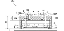
特許文献1に記載された従来の半導体パワーモジュールの一例を図6を参照して説明する。この従来の半導体パワーモジュール101では、天井部および側壁部を有するケース2内において、端子板7の一端は半導体チップ5と接続板6を介して接続され、ケース2外に露出した端子板7の他端部は直角に折り曲げられ、ケース2の天井部の外面と接触している。端子板7には貫通孔が設けられ、この貫通孔の内周に雌ネジ103が設けられている。雌ネジ103のある箇所に対応するケース2の天井部には凹型の深い孔104が設けられている。そして、主回路を構成するための外部導体9(例えば、バスバーなど。)を端子板7上に配置し、ボルト102を用いて、雄ネジが設けられた軸部102Aを端子板7の雌ネジ103に螺合して固着される。なお、図示しないが、当然、外部導体9には、ボルト102の軸部10Aが通る貫通孔が設けられる。
An example of a conventional semiconductor power module described in
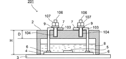
また、特許文献2に記載された従来の半導体モジュール201では、図7に示すように、前記ボルト102に代えて、雄ネジの設けられた棒状の軸部材106を使用し、ナット107を軸部材106の上端からねじ込むことにより、外部導体9と端子板7とを固定するように構成している。
Moreover, in the
しかし、このような従来のパワーモジュールの構造では、ボルト102の軸部102Aまたは軸部材106を収容するための深い穴104がケース2の天井部の外面から厚み方向に存在しているため、ケース2の天井部の厚み(D)を十分に厚く形成する必要がある。結果として、ケース2の側壁部を含めた全体の高さ(H)が高くなってしまい、小型化の要請に応えることが難しかった。
However, in such a conventional power module structure, since the
本発明は、上記の課題に鑑みて、ケースの薄型化に寄与しうる半導体パワーモジュールを提供することを目的とする。 An object of this invention is to provide the semiconductor power module which can contribute to thickness reduction of a case in view of said subject.
この発明の半導体パワーモジュールは、半導体チップ、ケース、ボルト、端子およびナットを有する。ケースは、前記半導体チップを覆うように配置される。ボルトは、頭部が前記ケースに埋設され、軸部が前記ケース外面から突出する。端子は、前記半導体チップおよび外部導体に接続される。ナットは、前記ボルトの軸部に螺合され、前記外部導体を前記端子と共に前記ケース外面に固定する。 The semiconductor power module of this invention has a semiconductor chip, a case, a bolt, a terminal, and a nut. The case is disposed so as to cover the semiconductor chip. The head of the bolt is embedded in the case, and the shaft portion protrudes from the outer surface of the case. The terminal is connected to the semiconductor chip and the external conductor. The nut is screwed into the shaft portion of the bolt, and fixes the outer conductor together with the terminal to the outer surface of the case.
この構成の半導体パワーモジュールによると、ボルトの軸部を収容するための深い穴をケースの厚み方向に設けることが不要であり、ケースの厚みとしては、ボルトの頭部を埋設可能な寸法が確保出来れば十分である。したがって、従来のものに比べてケースの厚みを大幅に削減出来る。 According to the semiconductor power module having this configuration, it is not necessary to provide a deep hole in the thickness direction of the case for accommodating the shaft portion of the bolt, and the thickness of the case ensures a dimension capable of embedding the bolt head. It is enough if possible. Therefore, the thickness of the case can be greatly reduced as compared with the conventional one.
なお、ボルトの頭部をケースに埋設するには、樹脂のインサート成型を利用して容易に実現出来る。或いは、ボルトの頭部が樹脂製のケース内に樹脂を充填することにより埋設されるようにしても良い。 In addition, embedding the bolt head in the case can be easily realized by using resin insert molding. Alternatively, the head of the bolt may be embedded by filling a resin case with resin.
また、前記端子の一例としては、帯状の板金から成る端子板が挙げられる。前記端子板の一端は半導体チップに接続され、前記端子板の他端部が前記ケースの外面に沿って前記ケースの外側へ導出されて前記ボルトの軸部に嵌合され、前記端子板と前記ナットとの間に前記外部導体が狭持される。 An example of the terminal is a terminal plate made of a strip-shaped sheet metal. One end of the terminal plate is connected to a semiconductor chip, and the other end portion of the terminal plate is led out of the case along the outer surface of the case and is fitted to a shaft portion of the bolt. The outer conductor is sandwiched between the nuts.
ケース外に露出した前記端子板は直角に折り曲げられる。したがって、端子板の他端部に折り曲げ方向に延びる長孔もしくは筋状の切り欠きを設けておくと、端子板の折り曲げ時にボルトの軸部の先端が端子板に当接することがない。 The terminal board exposed outside the case is bent at a right angle. Therefore, if a long hole or streak-like notch extending in the bending direction is provided at the other end portion of the terminal plate, the tip of the bolt shaft portion does not contact the terminal plate when the terminal plate is bent.
また、前記端子の他の例としては、前記ボルトの頭部が前記半導体チップに接続されることにより、前記ボルトが前記端子を兼ねるように構成することも可能である。 As another example of the terminal, it is possible to configure the bolt so that it also serves as the terminal by connecting the head of the bolt to the semiconductor chip.
この発明によれば、ケースの薄型化に寄与しうる半導体パワーモジュールを提供することが可能となる。 According to the present invention, it is possible to provide a semiconductor power module that can contribute to reducing the thickness of the case.
この発明の一実施形態に係る半導体パワーモジュールを図1〜図3を参照して説明する。 A semiconductor power module according to an embodiment of the present invention will be described with reference to FIGS.
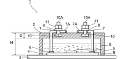
図1に示すように、この実施形態に係る半導体パワーモジュール1は、半導体チップ5、ケース2、ボルト11、端子板7およびナット11を有する。
As shown in FIG. 1, the
半導体チップ5は、基板4上の中央にマウントされる。本実施の形態では半導体チップ5が2端子素子(例えば、ダイオードなど。)である場合を示しているが、3端子以上の端子を持つ素子であっても構わない。半導体チップ5の各端子に対応して、基板4上の図面における左右両端部には、接続板6が2個設けられている。半導体チップ5の各端子と対応する接続板6とは、導体パターンや配線を用いて電気的に接続されている。
The
基板4は、冷却板3上に接着や溶接により固定されている。冷却板3の底面側には図示しないヒートシンクが取付けられ、基板4および冷却板3を介して半導体チップ5から発生する熱がヒートシンクに伝熱される。これにより、半導体パワーモジュール1の冷却構造が実現される。
The
ケース2は樹脂製である。ケース2は、側壁部と天井部を有し、底面が開放された箱型に形成されている。ケース2は、半導体チップ5および接続板6が搭載された基板4を覆うように、冷却板3上に嵌め込みやビス止め等で固定される。ケース2内には、半導体チップ5を汚れや湿気から保護するために、封止材8(例えば、モールド樹脂など。)が空間を残して詰められている。
ボルト10は、頭部がケース2の天井部に埋設され、雄ネジが設けられた軸部10Aがケース2の天井部外面から突出する。なお、ボルト10の頭部をケース2に埋設するには、樹脂のインサート成型を利用すれば容易に実現出来る。
The
端子板7は帯状の板金から出来ている。端子板7は、半導体チップ5と外部導体9に接続される本発明の端子の一例である。端子板7は基板4に対して略垂直に立設され、その一端(図1における下端)は接続板6に半田付け等により固定される。これにより、端子板7の一端と半導体チップ5が接続板6を介して電気的に接続される。
The
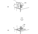
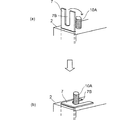
端子板7の他端部は、ケース2の天井部に設けられた貫通孔を貫通してケース2の外面に導出される。ケース2外に露出した端子板7の他端部は直角に折り曲げられ、図示のごとくケース2の外面と接触するようになる。端子板7の他端部には、ボルト10の軸部10Aが通るための貫通孔が設けられる。
The other end of the
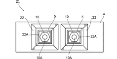
図2、図3は端子板7に設けられる貫通孔の例を示している。貫通孔を、折り曲げ方向に延びる長孔7A(図2参照。)もしくは筋状の切り欠き7B(図3参照。)として形成することにより、端子板7の折り曲げ時にボルト10の軸部10Aの先端が端子板7に当接することなく貫通孔に挿入される。これにより、端子板7の他端部を、ボルト10の軸部10Aに嵌合させることが出来る。
2 and 3 show examples of through holes provided in the
さらに、ボルト10の軸部10Aには端子板7の上から外部導体9(例えば、バスバーなど。)が取付けられる。このとき、ボルト10の軸部10Aが突出しているので、軸部10Aを外部導体9の取り付け用のガイドとすることが出来る。なお、図示しないが、当然、外部導体9には、ボルト10の軸部10Aが通る貫通孔が設けられる。
Further, an external conductor 9 (for example, a bus bar) is attached to the
そして、ナット11がボルト10の軸部10Aに螺合される。ナット11は、外部導体9を端子板4と共にケース2外面に固定するものである。
Then, the
本実施の形態に係る半導体パワーモジュール1によると、従来の半導体パワーモジュールのように、ボルトの軸部もしくは軸部材を収容するための深い穴104(図5、図6参照。)をケース2の厚み方向に設けることが不要であり、ケース2の天井部の厚み(D)としては、ボルト10の頭部を埋設可能な寸法が確保出来れば十分である。したがって、従来のものに比べてケース2の天井部の厚み(D)を大幅に削減出来、ひいてはケース2の側壁部を含む全体の高さ(H)を低減できる。これにより、製品の小型化の要請に答えることが出来る。また、ケース2の材料である樹脂の使用量も削減され、製品価格の低下にも寄与する。
According to the
次に、本発明の第2の実施形態に係る半導体パワーモジュールについて図4、図5を参照して説明する。この図において、上記第1の実施形態に係るパワーモジュールと同一部材には同一符号を付している。 Next, a semiconductor power module according to a second embodiment of the present invention will be described with reference to FIGS. In this figure, the same reference numerals are assigned to the same members as those of the power module according to the first embodiment.
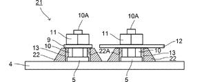
本実施の形態に係る半導体パワーモジュール21では、図4に示すように、この基板4上に半導体チップ5がマウントされ、半導体チップ5の上面に、半田や接着剤等によりボルト10の頭部の図で見て底面が固着され、半導体チップ5とボルト10自体が電気的に接続される。すなわち、本実施の形態では、ボルト10が、半導体チップ5を外部導体9に接続させるための端子を兼ねている。ケース22は台状を呈し、底面から高さ方向に延びる筒状の開口22Aを有している。ケース22の開口22Aをボルト10の頭部に被せ、その後開口22Aに樹脂13を充填してボルト10の頭部を埋設する。図4で示すこの状態ではボルト10の軸部10Aはケース22外の上方に突出している。なお、ケース22は開口22Aの下方が少なくとも半導体チップ5よりも大きな錐台状でもよく、その場合は上方が窄んでいる分、充填させる樹脂は少なくて済む。本例では開口22Aの上方はボルト10の頭部より大きければ良く、開口22Aの形状としては柱状をしていても錐台状をしていても構わない。本例では半導体チップ5が開口22Aよりも小さな場合を示したが、半導体チップ5が開口22A上方よりも大きい場合には、開口22Aが下方に向けて大きくなる錐台状としても、開口22Aの下方に段差を設けて半導体チップ5を覆うようにしても良い。
In the
ケース22の高さは、半導体チップ5とボルト10の頭部を合わせた高さと略同一の寸法に設定されており、ボルト10の頭部の図で見て上面(軸部10Aが形成された面)が露出している。他の基板12や外部導体9の貫通孔をボルト10の軸部10Aに通し、ボルト10の露出した面に他の基板12や外部導体9を載せ、ナット11をボルト10の軸部10Aに螺合させる。ナット11は、他の基板12や外部導体9をケース2外面に固定するものである。
The height of the
このようにボルト10の露出面に他の基板12や外部導体9を載せて取り付けるため、ボルト10の露出面を放熱板として利用でき、高い放熱効果を得ることができる。なお、本例ではボルト10の上端を露出させた例を示したが、ボルト10の頭部を完全に埋設するようにし、他の基板などの取り付け高さを調整することもできる。その場合でも、半導体チップ5の熱が直接ボルト10を通じて外部に伝わるため、放熱効果を得ることができる。
Thus, since the other board |
特に、本実施の形態に係る半導体パワーモジュール21によると、第1の実施形態のような端子板7(図1参照。)が不要であるため、ボルト10は、軸部10Aの短いものを使用することが可能となる。また、ナット11は、外部導体9のみを固定できれば良いため、高さ寸法の小さいものを選んで使用することが可能となる。したがって、半導体パワーモジュールを極めて小型に構成することが可能となる。
In particular, according to the
上述の実施形態の説明は、すべての点で例示であって、制限的なものではないと考えられるべきである。この発明の範囲は、上述の実施形態ではなく、特許請求の範囲によって示される。さらに、この発明の範囲には、特許請求の範囲と均等の意味および範囲内でのすべての変更が含まれることが意図される。 The above description of the embodiment is to be considered in all respects as illustrative and not restrictive. The scope of the present invention is shown not by the above-described embodiments but by the claims. Furthermore, the scope of the present invention is intended to include all modifications within the meaning and scope equivalent to the claims.
1,21…半導体パワーモジュール
2,22…ケース
4…基板
5…半導体チップ
6…接続板
7…端子板
9…外部導体
10…ボルト
10A…ボルトの軸部
11…ナット
DESCRIPTION OF
Claims (6)
前記半導体チップを覆うように配置されるケースと、
頭部が前記ケースに埋設され、軸部が前記ケース外面から突出するボルトと、
前記半導体チップおよび外部導体に接続される端子と、
前記ボルトの軸部に螺合され、前記外部導体を前記端子と共に前記ケース外面に固定するナットと、
を有する半導体パワーモジュール。 A semiconductor chip and a case arranged to cover the semiconductor chip;
A bolt with a head embedded in the case and a shaft protruding from the outer surface of the case;
Terminals connected to the semiconductor chip and the external conductor;
A nut that is screwed onto the shaft of the bolt and fixes the outer conductor to the outer surface of the case together with the terminal;
A semiconductor power module.
Priority Applications (1)
| Application Number | Priority Date | Filing Date | Title |
|---|---|---|---|
| JP2010291429A JP2012138531A (en) | 2010-12-28 | 2010-12-28 | Semiconductor power module |
Applications Claiming Priority (1)
| Application Number | Priority Date | Filing Date | Title |
|---|---|---|---|
| JP2010291429A JP2012138531A (en) | 2010-12-28 | 2010-12-28 | Semiconductor power module |
Publications (1)
| Publication Number | Publication Date |
|---|---|
| JP2012138531A true JP2012138531A (en) | 2012-07-19 |
Family
ID=46675705
Family Applications (1)
| Application Number | Title | Priority Date | Filing Date |
|---|---|---|---|
| JP2010291429A Pending JP2012138531A (en) | 2010-12-28 | 2010-12-28 | Semiconductor power module |
Country Status (1)
| Country | Link |
|---|---|
| JP (1) | JP2012138531A (en) |
Cited By (5)
| Publication number | Priority date | Publication date | Assignee | Title |
|---|---|---|---|---|
| JP2013062406A (en) * | 2011-09-14 | 2013-04-04 | Shindengen Electric Mfg Co Ltd | Semiconductor device |
| CN105765716A (en) * | 2014-05-15 | 2016-07-13 | 富士电机株式会社 | Power semiconductor module and composite module |
| CN106531693A (en) * | 2015-09-15 | 2017-03-22 | 富士电机株式会社 | Semiconductor device |
| JP2018113368A (en) * | 2017-01-12 | 2018-07-19 | 三菱電機株式会社 | Semiconductor module |
| WO2019087327A1 (en) * | 2017-11-01 | 2019-05-09 | 三菱電機株式会社 | Semiconductor device, production method therefor, and automobile |
Citations (4)
| Publication number | Priority date | Publication date | Assignee | Title |
|---|---|---|---|---|
| JPS61501602A (en) * | 1984-03-05 | 1986-07-31 | ヒユ−ズ・エアクラフト・カンパニ− | Thermal Activated Shorting Diode Switch with Junction Path of Non-Change Operation |
| JPS61232644A (en) * | 1985-04-08 | 1986-10-16 | Mitsubishi Electric Corp | Semiconductor device |
| JPH0494155A (en) * | 1990-08-09 | 1992-03-26 | Fuji Electric Co Ltd | Externally-led terminal of semiconductor device |
| JPH0922973A (en) * | 1995-07-07 | 1997-01-21 | Mitsubishi Electric Corp | Semiconductor device |
-
2010
- 2010-12-28 JP JP2010291429A patent/JP2012138531A/en active Pending
Patent Citations (4)
| Publication number | Priority date | Publication date | Assignee | Title |
|---|---|---|---|---|
| JPS61501602A (en) * | 1984-03-05 | 1986-07-31 | ヒユ−ズ・エアクラフト・カンパニ− | Thermal Activated Shorting Diode Switch with Junction Path of Non-Change Operation |
| JPS61232644A (en) * | 1985-04-08 | 1986-10-16 | Mitsubishi Electric Corp | Semiconductor device |
| JPH0494155A (en) * | 1990-08-09 | 1992-03-26 | Fuji Electric Co Ltd | Externally-led terminal of semiconductor device |
| JPH0922973A (en) * | 1995-07-07 | 1997-01-21 | Mitsubishi Electric Corp | Semiconductor device |
Cited By (8)
| Publication number | Priority date | Publication date | Assignee | Title |
|---|---|---|---|---|
| JP2013062406A (en) * | 2011-09-14 | 2013-04-04 | Shindengen Electric Mfg Co Ltd | Semiconductor device |
| CN105765716A (en) * | 2014-05-15 | 2016-07-13 | 富士电机株式会社 | Power semiconductor module and composite module |
| CN106531693A (en) * | 2015-09-15 | 2017-03-22 | 富士电机株式会社 | Semiconductor device |
| JP2018113368A (en) * | 2017-01-12 | 2018-07-19 | 三菱電機株式会社 | Semiconductor module |
| WO2019087327A1 (en) * | 2017-11-01 | 2019-05-09 | 三菱電機株式会社 | Semiconductor device, production method therefor, and automobile |
| JPWO2019087327A1 (en) * | 2017-11-01 | 2020-04-23 | 三菱電機株式会社 | Semiconductor device, manufacturing method thereof, and automobile |
| CN111279475A (en) * | 2017-11-01 | 2020-06-12 | 三菱电机株式会社 | Semiconductor device, method for manufacturing same, and automobile |
| US11251098B2 (en) | 2017-11-01 | 2022-02-15 | Mitsubishi Electric Corporation | Semiconductor device, production method therefor, and automobile |
Similar Documents
| Publication | Publication Date | Title |
|---|---|---|
| JP6252871B2 (en) | Circuit structure and electrical junction box | |
| US9698507B2 (en) | Package structure of power module | |
| JP6521171B2 (en) | Circuit structure | |
| JP2012138531A (en) | Semiconductor power module | |
| JP2014138442A (en) | Motor driving device having radiator | |
| WO2015025447A1 (en) | Semiconductor devices | |
| US8169069B2 (en) | Integrated semiconductor outline package | |
| US9704776B2 (en) | Semiconductor device having semiconductor module and cooler coupled with bolt | |
| JP5556531B2 (en) | Electronic module mounting structure | |
| US20060267180A1 (en) | Heat sink arrangement for electrical apparatus | |
| WO2017098703A1 (en) | Heat radiating device for heat generating electronic component, manufacturing method thereof, and vehicle-mounted charger | |
| JP5787435B2 (en) | Semiconductor heat dissipation device | |
| JP2009295706A (en) | Electronic controller | |
| US11533819B2 (en) | Method for manufacturing a stack structure | |
| JP5764443B2 (en) | Semiconductor device | |
| JP4588774B2 (en) | Exterior resin case for semiconductor devices | |
| JP2011082344A (en) | Method for locking electronic component and electronic apparatus | |
| JP6409879B2 (en) | Packaged power semiconductor and packaged power semiconductor mounting structure | |
| KR102333657B1 (en) | Power module | |
| JP4513560B2 (en) | Power module and air conditioner | |
| JP7466850B2 (en) | On-board chargers and inverters | |
| JP7026865B1 (en) | Power module | |
| JP7056366B2 (en) | Semiconductor modules and semiconductor devices using them | |
| JP2005158918A (en) | Packaging resin case for semiconductor device | |
| KR102333646B1 (en) | Power module |
Legal Events
| Date | Code | Title | Description |
|---|---|---|---|
| A621 | Written request for application examination |
Free format text: JAPANESE INTERMEDIATE CODE: A621 Effective date: 20131115 |
|
| A977 | Report on retrieval |
Free format text: JAPANESE INTERMEDIATE CODE: A971007 Effective date: 20140630 |
|
| A131 | Notification of reasons for refusal |
Free format text: JAPANESE INTERMEDIATE CODE: A131 Effective date: 20140708 |
|
| A02 | Decision of refusal |
Free format text: JAPANESE INTERMEDIATE CODE: A02 Effective date: 20141111 |