JP2012109382A - Connection structure and method of circuit board and lead wire - Google Patents
Connection structure and method of circuit board and lead wire Download PDFInfo
- Publication number
- JP2012109382A JP2012109382A JP2010256755A JP2010256755A JP2012109382A JP 2012109382 A JP2012109382 A JP 2012109382A JP 2010256755 A JP2010256755 A JP 2010256755A JP 2010256755 A JP2010256755 A JP 2010256755A JP 2012109382 A JP2012109382 A JP 2012109382A
- Authority
- JP
- Japan
- Prior art keywords
- lead wire
- circuit board
- lead wires
- connection structure
- hole
- Prior art date
- Legal status (The legal status is an assumption and is not a legal conclusion. Google has not performed a legal analysis and makes no representation as to the accuracy of the status listed.)
- Granted
Links
Images


Abstract
Description
本発明は、回路基板とリード線との接続構造及び方法に係り、特に、車両等の振動状況下で用いるのに好適な回路基板とリード線との接続構造及び方法に関するものである。 The present invention relates to a circuit board and lead wire connection structure and method, and more particularly, to a circuit board and lead wire connection structure and method suitable for use in vibration conditions of a vehicle or the like.
通常、回路基板とリード線とを接続する場合、例えば、特許文献1に記載されているように、回路基板の接続部にリード線の導体露出部を接触させ、はんだ付け等により接合して電気的に接続する。
Normally, when connecting a circuit board and a lead wire, for example, as described in
ところが、はんだ接合による回路基板とリード線との接続構造(以下、単に接続構造ともいう)を車両等の振動状況下で用いた場合(例えば、車載センサのリード線とECUの回路基板とを接続する場合等)、振動により回路基板とリード線との接合部に外力が加わり、リード線が外れたりして信頼性上好ましくない。 However, when a connection structure between a circuit board and a lead wire by soldering (hereinafter also simply referred to as a connection structure) is used under vibration conditions of a vehicle or the like (for example, connecting a lead wire of an in-vehicle sensor and a circuit board of an ECU) Etc.), an external force is applied to the joint between the circuit board and the lead wire due to vibration, and the lead wire is detached, which is not preferable in terms of reliability.
この問題を克服すべく、車両等の振動状況下では、振動によって生じる接合部への影響を低減するために抵抗溶接による接続構造を用いることが多い。抵抗溶接は、はんだ接合よりも接合強度が高く信頼性に優れるが、接合時に回路基板を破壊してしまう虞がある。即ち、はんだ接合の場合は、回路基板の接続部をはんだの融点(組成にもよるが200℃前後)まで加熱すれば接合が可能であるが、抵抗溶接の場合は、接続する材料の融点(例えば、リード線の導体露出部及び回路基板の接続部は主に銅で形成されており、この場合融点は1000℃以上)まで加熱しなければならず、加熱時の熱で回路基板を破壊してしまう虞がある。そのため、リード線を回路基板に直接、抵抗溶接することは好ましくないので、以下のような構造を採用している。 In order to overcome this problem, a connection structure by resistance welding is often used to reduce the influence on the joint caused by vibration under vibration conditions of a vehicle or the like. Resistance welding has higher bonding strength and higher reliability than solder bonding, but may damage the circuit board during bonding. That is, in the case of solder joining, joining is possible by heating the connection part of the circuit board to the melting point of the solder (depending on the composition, but around 200 ° C.), but in the case of resistance welding, the melting point of the material to be connected ( For example, the conductor exposed portion of the lead wire and the connection portion of the circuit board are mainly formed of copper, and in this case, the melting point must be heated to 1000 ° C. or higher), and the circuit board is destroyed by the heat during heating. There is a risk that. Therefore, it is not preferable to resistance-weld the lead wire directly to the circuit board, so the following structure is adopted.
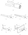
図4に示すように、抵抗溶接による接続構造30は、リード線31と、スルーホール32が形成された回路基板33と、プレス成形により形成された端子部品34がインサート成形されてなる端子インサート基板ホルダ35と、を備える。
As shown in FIG. 4, the
この接続構造30においては、図5(a)〜(c)に示すように、リード線31の素線固めされた導体露出部36が端子部品34の接続端子37に抵抗溶接され、端子部品34のスルーホール挿入ピン部38が回路基板33のスルーホール32に挿入されると共にはんだ接合されて、リード線31と回路基板33とが端子部品34を介して接続されている。なお、図5(a),(b)では端子部品34のみを、図5(c)ではリード線31と回路基板33と端子部品34のみを図示している。
In this
このように、リード線31と端子部品34とを接合強度の高い抵抗溶接で接続し、回路基板33と端子部品34とを振動でも接続が外れにくいスルーホール32及びスルーホール挿入ピン部38を用いた方法で接続することで、振動に強い接続構造を実現している。
In this way, the
しかしながら、抵抗溶接による接続構造では、端子部品を介してリード線と回路基板とを接続する必要があるため、はんだ接合による接続構造に比べて、端子部品の分だけ部品点数が増大してしまうという問題や、端子部品のプレス成形、及び端子部品のインサート成形のために、高コストになってしまうという問題があった。 However, in the connection structure by resistance welding, since it is necessary to connect the lead wire and the circuit board via the terminal component, the number of components increases by the amount of the terminal component compared to the connection structure by solder bonding. There is a problem that the cost becomes high due to the problem and the press molding of the terminal parts and the insert molding of the terminal parts.
また、抵抗溶接のためにリード線を端子部品の溶接位置へ位置決めする必要があるが、この位置決めが複雑で自動化が困難であるため、手作業に頼る部分が多く、高コストになってしまっていた。 In addition, it is necessary to position the lead wire to the welding position of the terminal parts for resistance welding, but this positioning is complicated and difficult to automate, so there are many parts that rely on manual work, and the cost is high. It was.
更に、リード線と端子部品、スルーホールとスルーホール挿入ピン部の2箇所で接続を行うため、信頼性を確保するための導通確認を2箇所で行う必要があり、面倒であるという問題があった。 In addition, since the connection is made at two locations of the lead wire and the terminal component, the through hole and the through hole insertion pin portion, it is necessary to confirm the continuity to ensure reliability at two locations, which is troublesome. It was.
そこで、本発明の目的は、前記課題を解決し、振動環境下においても信頼性の向上が可能であり、且つ、製造コストの低コスト化に寄与することが可能であり、更には、信頼性を確保するための導通確認の簡素化に寄与することが可能な回路基板とリード線との接続構造及び方法を提供することにある。 Therefore, the object of the present invention is to solve the above problems, improve the reliability even in a vibration environment, contribute to the reduction of the manufacturing cost, and further improve the reliability. It is an object to provide a connection structure and a method for connecting a circuit board and a lead wire that can contribute to simplification of confirmation of continuity in order to ensure the resistance.
この目的を達成するために創案された本発明は、複数のスルーホールが形成された回路基板と、前記複数のスルーホールのいずれかに挿入されて接続されるスルーホール挿入ピン部を有する複数のリード線と、前記複数のリード線の前記スルーホール挿入ピン部のそれぞれが対応する前記スルーホールに挿入されるように、前記複数のリード線を位置決め固定するリード線固定部材と、を備え、前記スルーホール挿入ピン部は、前記リード線の導体露出部に曲げ加工を施して形成される回路基板とリード線との接続構造である。 The present invention devised to achieve this object includes a circuit board having a plurality of through holes and a plurality of through hole insertion pin portions that are inserted into and connected to any of the plurality of through holes. A lead wire fixing member that positions and fixes the plurality of lead wires so that each of the through hole insertion pin portions of the plurality of lead wires is inserted into the corresponding through hole, and The through-hole insertion pin portion is a connection structure between a circuit board and a lead wire formed by bending a conductor exposed portion of the lead wire.
前記リード線の導体露出部は、前記リード線の露出された導体を素線固めして形成されると良い。 The conductor exposed portion of the lead wire may be formed by solidifying the exposed conductor of the lead wire.
前記リード線固定部材は、前記スルーホールに挿入される前記スルーホール挿入ピン部の端部を除く前記リード線の端部を覆うように形成されると共に、前記回路基板を載置するための台座部を有すると良い。 The lead wire fixing member is formed so as to cover an end portion of the lead wire excluding an end portion of the through hole insertion pin portion inserted into the through hole, and a base for mounting the circuit board It is good to have a part.
また、本発明は、回路基板に複数のスルーホールを形成し、複数のリード線のそれぞれを段剥きして導体を露出させ、前記複数のリード線の露出された前記導体を素線固めして導体露出部を形成し、前記複数のリード線の前記導体露出部のそれぞれに曲げ加工を施して、前記複数のスルーホールのいずれかに挿入するためのスルーホール挿入ピン部を形成し、前記複数のリード線の前記スルーホール挿入ピン部のそれぞれが対応する前記スルーホールに挿入されるように、前記複数のリード線を位置決め固定し、前記複数のリード線の前記スルーホール挿入ピン部のそれぞれを対応する前記スルーホールに挿入すると共に接合して、前記回路基板と前記リード線を接続し、前記リード線と接続した前記回路基板を樹脂でポッティグする回路基板とリード線との接続方法である。 The present invention also includes forming a plurality of through holes in the circuit board, stepping off each of the plurality of lead wires to expose the conductor, and solidifying the exposed conductor of the plurality of lead wires. Forming a conductor exposed portion, bending each of the conductor exposed portions of the plurality of lead wires to form a through-hole insertion pin portion for insertion into any of the plurality of through-holes; The plurality of lead wires are positioned and fixed so that each of the through hole insertion pin portions of the lead wires is inserted into the corresponding through hole, and each of the through hole insertion pin portions of the plurality of lead wires is fixed. A circuit board for inserting and joining the corresponding through hole to connect the circuit board and the lead wire, and potting the circuit board connected to the lead wire with resin. As a method of connecting the lead wires.
本発明によれば、振動環境下においても信頼性の向上が可能であり、且つ、製造コストの低コスト化に寄与することが可能であり、更には、信頼性を確保するための導通確認の簡素化に寄与することが可能な回路基板とリード線との接続構造及び方法を提供することができる。 According to the present invention, it is possible to improve the reliability even in a vibration environment, contribute to the reduction of the manufacturing cost, and further confirm the continuity for ensuring the reliability. A circuit board-lead wire connecting structure and method that can contribute to simplification can be provided.
以下、本発明の好適な実施の形態を添付図面にしたがって説明する。 Preferred embodiments of the present invention will be described below with reference to the accompanying drawings.
図1は、本発明の好適な実施の形態に係る回路基板とリード線との接続構造を示す図である。 FIG. 1 is a diagram showing a connection structure between a circuit board and lead wires according to a preferred embodiment of the present invention.
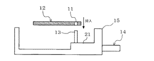
図1に示すように、本実施の形態に係る回路基板とリード線との接続構造10は、複数のスルーホール11が形成された回路基板12と、複数のスルーホール11のいずれかに挿入されて接続されるスルーホール挿入ピン部13を有する複数のリード線14と、複数のリード線14のスルーホール挿入ピン部13のそれぞれが対応するスルーホール11に挿入されるように、複数のリード線14を位置決め固定するリード線固定部材15と、を備え、スルーホール挿入ピン部13は、リード線14の導体露出部20に曲げ加工を施して形成される。
As shown in FIG. 1, the circuit board-lead
この接続構造10の構成を、回路基板12とリード線14の接続方法と共に説明する。
The configuration of the
先ず、回路基板12に複数のスルーホール11を形成する。この回路基板12は、図4で説明した従来の接続構造30で用いていたものをそのまま転用することが可能であり、格別工程が増加する訳ではない。
First, a plurality of through
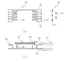
他方、図2(a),(b)に示すように、複数のリード線14のそれぞれを段剥きして導体16を露出させておく。図2(a)では、複数本(例えば7本)の素線からなる導体16(撚線)とその外周に被覆された絶縁体17とを有する2本のリード線14がシース18により束ねられたケーブル19を用いる例を示しているが、リード線14の形態はこれに限定されるものではない。例えば、リード線14は、導体16のみからなるものであっても良いし、絶縁体17とシース18との間に介在物を有するものであっても良い。
On the other hand, as shown in FIGS. 2A and 2B, each of the plurality of
次いで、図2(c)に示すように、複数のリード線14の露出された導体16を素線固めして導体露出部20を形成する。この素線固めは、例えば超音波溶着によって行うと良い。これにより、導体露出部20はリジッドに形成される。
Next, as shown in FIG. 2C, the exposed
その後、図2(d)に示すように、複数のリード線14の導体露出部20のそれぞれに曲げ加工を施して、複数のスルーホール11のいずれかに挿入するためのスルーホール挿入ピン部13を形成する。これにより、リード線14の導体露出部20自体がリジッドなスルーホール挿入ピン部13となる。
Thereafter, as shown in FIG. 2 (d), each of the conductor exposed
そして、図2(e)に示すように、複数のリード線14のスルーホール挿入ピン部13のそれぞれが対応するスルーホール11に挿入されるように、複数のリード線14を位置決め固定する。
Then, as shown in FIG. 2 (e), the plurality of
この位置決め固定は、複数のリード線14のスルーホール挿入ピン部13のそれぞれが対応するスルーホール11に挿入されるように、複数のリード線14のそれぞれを位置決めして(金型に形成された溝等に)保持しておき、複数のリード線14の絶縁体17の部分に樹脂を射出成形して行う。この射出成形された樹脂が、複数のリード線14を位置決め固定するためのリード線固定部材15となる。なお、前工程の曲げ加工と本工程の射出成形を同時に実施することも可能である。これにより、工程を1つ減らすことができる。
This positioning and fixing is performed by positioning each of the plurality of
その後、複数のリード線14のスルーホール挿入ピン部13のそれぞれを対応するスルーホール11に挿入すると共にはんだ接合等により接合して、回路基板12とリード線14を接続する。
Thereafter, each of the through-hole
最後に、リード線14と接続した回路基板12をエポキシ等の樹脂でポッティグして、構造の気密性を確保する。
Finally, the
以上の工程により、接続構造10が得られる。
The
この接続構造10では、スルーホール11にスルーホール挿入ピン部13を挿入して接続する構造としているため、強固な接続を実現でき、車両等の振動環境下で用いたときの信頼性が高い。
In this
また、リード線14の導体露出部20を直接にスルーホール挿入ピン部13として加工しているので、従来の接続構造に比べて、端子部品の分だけ部品点数を削減することができ、端子部品のプレス成形、及び端子部品のインサート成形が必要ないので、低コストでリード線14と回路基板12を接続することができる。
Moreover, since the conductor exposed
なお、リード線14の射出成形が必要なことを考慮すると、成形費用はインサート成形を行う従来と同程度になる可能性はあるが、端子部品、及び抵抗溶接工程が無くなることを考えれば、顕著な低コスト化が期待できる。
In consideration of the necessity of injection molding of the
また、接続構造10では、複数のリード線14を金型に形成された溝等に保持した上で樹脂を射出成形することで、予めリード線固定部材15で位置決め固定しているので、複数のリード線14が位置決めされて保持されるような形状の金型を一度作製してしまえば、その後は位置決めの手間が省ける。つまり、手作業に頼る必要がなく、複数のリード線14を金型に機械的に保持させれば自動的に位置決めされた状態で射出成形が行われる。そのため、人件費を削減することが可能となり、製造コストの低減に寄与することができる。
Further, in the
更に、スルーホール11とスルーホール挿入ピン部13の1箇所で接続を行うため、従来に比べて導通確認を行う箇所を半分に減らすことができる。
Furthermore, since the connection is made at one place of the through
また、リード線14の導体露出部20をリジッドに形成しているため、導体露出部20をスルーホール挿入ピン部13とし、これをスルーホール11に挿入する際に、スルーホール挿入ピン部13に曲げが生じず挿入が容易である。
Further, since the conductor exposed
また、従来の接続構造では抵抗溶接のためのスペースが必要であるが、本実施の形態に係る接続構造10では、リード線14を回路基板12に直接接続するため、前記のスペースを必要とせず構造の小型化を図ることができる。
In addition, in the conventional connection structure, a space for resistance welding is required. However, in the
以上、要するに、本発明によれば、振動環境下においても信頼性の向上が可能であり、且つ、製造コストの低コスト化に寄与することが可能であり、更には、信頼性を確保するための導通確認の簡素化に寄与することが可能な回路基板とリード線との接続構造及び方法を提供することができる。 As described above, according to the present invention, the reliability can be improved even in a vibration environment, the manufacturing cost can be reduced, and further, the reliability can be ensured. It is possible to provide a circuit board-lead wire connecting structure and method that can contribute to simplification of continuity confirmation.
なお、本発明は前記の実施の形態に限定されるものではなく、本発明の趣旨を逸脱しない範囲で種々の変更が可能である。 The present invention is not limited to the above-described embodiments, and various modifications can be made without departing from the spirit of the present invention.
例えば、リード線固定部材15を、図3に示すように、スルーホール11に挿入されるスルーホール挿入ピン部13の端部を除くリード線14の端部を覆うように形成すると共に、回路基板12を載置するための台座部21を有するように構成しても良い。
For example, as shown in FIG. 3, the lead
この場合、リード線固定部材15が回路基板12のケースを兼ねる。ポッティグの際には、ケース内をエポキシ等の樹脂で埋めるようにポッティグすると良い。
In this case, the lead
このような構造によれば、リード線14の端部までリード線固定部材15により固定されるため、前記の実施の形態に比べてリード線14を強固に固定することができると共に、リード線14の位置決め精度を向上させることができるという付加的な効果が得られる。
According to such a structure, the
10 接続構造
11 スルーホール
12 回路基板
13 スルーホール挿入ピン部
14 リード線
15 リード線固定部材
16 導体
17 絶縁体
18 シース
19 ケーブル
20 導体露出部
21 台座部
DESCRIPTION OF
Claims (4)
前記複数のスルーホールのいずれかに挿入されて接続されるスルーホール挿入ピン部を有する複数のリード線と、
前記複数のリード線の前記スルーホール挿入ピン部のそれぞれが対応する前記スルーホールに挿入されるように、前記複数のリード線を位置決め固定するリード線固定部材と、 を備え、
前記スルーホール挿入ピン部は、前記リード線の導体露出部に曲げ加工を施して形成されることを特徴とする回路基板とリード線との接続構造。 A circuit board on which a plurality of through holes are formed;
A plurality of lead wires having a through-hole insertion pin portion inserted into and connected to any of the plurality of through-holes;
A lead wire fixing member for positioning and fixing the plurality of lead wires so that each of the through hole insertion pin portions of the plurality of lead wires is inserted into the corresponding through hole, and
The through-hole insertion pin portion is formed by bending a conductor exposed portion of the lead wire to form a connection structure between the circuit board and the lead wire.
複数のリード線のそれぞれを段剥きして導体を露出させ、
前記複数のリード線の露出された前記導体を素線固めして導体露出部を形成し、
前記複数のリード線の前記導体露出部のそれぞれに曲げ加工を施して、前記複数のスルーホールのいずれかに挿入するためのスルーホール挿入ピン部を形成し、
前記複数のリード線の前記スルーホール挿入ピン部のそれぞれが対応する前記スルーホールに挿入されるように、前記複数のリード線を位置決め固定し、
前記複数のリード線の前記スルーホール挿入ピン部のそれぞれを対応する前記スルーホールに挿入すると共に接合して、前記回路基板と前記リード線を接続し、
前記リード線と接続した前記回路基板を樹脂でポッティグすることを特徴とする回路基板とリード線との接続方法。 Form multiple through holes in the circuit board,
Strip each of the multiple lead wires to expose the conductor,
The exposed conductor of the plurality of lead wires is solidified to form a conductor exposed portion,
Bending each of the conductor exposed portions of the plurality of lead wires to form a through hole insertion pin portion for insertion into any of the plurality of through holes,
Positioning and fixing the plurality of lead wires so that each of the through-hole insertion pin portions of the plurality of lead wires is inserted into the corresponding through-hole,
Inserting and joining each of the through hole insertion pin portions of the plurality of lead wires into the corresponding through hole, connecting the circuit board and the lead wire,
A method of connecting a circuit board and a lead wire, wherein the circuit board connected to the lead wire is potted with resin.
Priority Applications (1)
| Application Number | Priority Date | Filing Date | Title |
|---|---|---|---|
| JP2010256755A JP5556609B2 (en) | 2010-11-17 | 2010-11-17 | Connection structure between circuit board and lead wire |
Applications Claiming Priority (1)
| Application Number | Priority Date | Filing Date | Title |
|---|---|---|---|
| JP2010256755A JP5556609B2 (en) | 2010-11-17 | 2010-11-17 | Connection structure between circuit board and lead wire |
Publications (2)
| Publication Number | Publication Date |
|---|---|
| JP2012109382A true JP2012109382A (en) | 2012-06-07 |
| JP5556609B2 JP5556609B2 (en) | 2014-07-23 |
Family
ID=46494693
Family Applications (1)
| Application Number | Title | Priority Date | Filing Date |
|---|---|---|---|
| JP2010256755A Expired - Fee Related JP5556609B2 (en) | 2010-11-17 | 2010-11-17 | Connection structure between circuit board and lead wire |
Country Status (1)
| Country | Link |
|---|---|
| JP (1) | JP5556609B2 (en) |
Cited By (2)
| Publication number | Priority date | Publication date | Assignee | Title |
|---|---|---|---|---|
| US20170222387A1 (en) * | 2016-01-29 | 2017-08-03 | The Boeing Company | Vibrating pallet system for automated wire insertion |
| CN109510361A (en) * | 2018-12-27 | 2019-03-22 | 长沙理工大学 | A kind of three phase induction generator stator lead-out wire connection structure |
Citations (5)
| Publication number | Priority date | Publication date | Assignee | Title |
|---|---|---|---|---|
| JPS5691492A (en) * | 1979-12-26 | 1981-07-24 | Hitachi Ltd | Method of mounting lead wire |
| JPS58141512U (en) * | 1982-03-19 | 1983-09-24 | 渡邊 和彦 | Wiring material assembly |
| JPH0292971U (en) * | 1989-01-12 | 1990-07-24 | ||
| JPH0496886U (en) * | 1991-01-31 | 1992-08-21 | ||
| JPH1012289A (en) * | 1996-06-19 | 1998-01-16 | Mitsubishi Electric Corp | Electric connection terminal and manufacture therefor |
-
2010
- 2010-11-17 JP JP2010256755A patent/JP5556609B2/en not_active Expired - Fee Related
Patent Citations (5)
| Publication number | Priority date | Publication date | Assignee | Title |
|---|---|---|---|---|
| JPS5691492A (en) * | 1979-12-26 | 1981-07-24 | Hitachi Ltd | Method of mounting lead wire |
| JPS58141512U (en) * | 1982-03-19 | 1983-09-24 | 渡邊 和彦 | Wiring material assembly |
| JPH0292971U (en) * | 1989-01-12 | 1990-07-24 | ||
| JPH0496886U (en) * | 1991-01-31 | 1992-08-21 | ||
| JPH1012289A (en) * | 1996-06-19 | 1998-01-16 | Mitsubishi Electric Corp | Electric connection terminal and manufacture therefor |
Cited By (5)
| Publication number | Priority date | Publication date | Assignee | Title |
|---|---|---|---|---|
| US20170222387A1 (en) * | 2016-01-29 | 2017-08-03 | The Boeing Company | Vibrating pallet system for automated wire insertion |
| US10109974B2 (en) * | 2016-01-29 | 2018-10-23 | The Boeing Company | Vibrating pallet system for automated wire insertion |
| US11271353B2 (en) | 2016-01-29 | 2022-03-08 | The Boeing Company | Vibrating pallet system for automated wire insertion |
| CN109510361A (en) * | 2018-12-27 | 2019-03-22 | 长沙理工大学 | A kind of three phase induction generator stator lead-out wire connection structure |
| CN109510361B (en) * | 2018-12-27 | 2024-02-02 | 长沙理工大学 | Stator outgoing line connection structure of three-phase asynchronous generator |
Also Published As
| Publication number | Publication date |
|---|---|
| JP5556609B2 (en) | 2014-07-23 |
Similar Documents
| Publication | Publication Date | Title |
|---|---|---|
| JP5589778B2 (en) | Connection structure and connection method for differential signal transmission cable and circuit board | |
| JP5904107B2 (en) | Cable connector, cable assembly, and method of manufacturing cable assembly | |
| JP5177582B2 (en) | Electromagnetic coil device | |
| US20120318576A1 (en) | Connecting structure and connecting method for electric cables | |
| CN104641426A (en) | Terminal-formed wire and method for manufacturing said terminal-formed wire | |
| JP2009063527A (en) | Current detector | |
| US8614399B2 (en) | Electric junction box | |
| JP5556609B2 (en) | Connection structure between circuit board and lead wire | |
| JP6941731B2 (en) | Manufacturing method of stranded wire connector and stranded wire connector for electric devices | |
| CN211126117U (en) | Cable assembly | |
| JP6042635B2 (en) | Electrical wire terminal treatment method | |
| US20230032339A1 (en) | Circuit board for stator windings having integral securing structures | |
| JP5141917B2 (en) | Mounting board | |
| EP2518743B1 (en) | Electronic component device | |
| US20130113590A1 (en) | Inductive component and manufacturing method thereof | |
| JP2017139394A (en) | Electric connection structure and method for electronic circuit board and fpc | |
| JP6381439B2 (en) | Cable connection structure | |
| JP6674847B2 (en) | Motor stator assembling method and motor stator structure | |
| JP2014096224A (en) | Flat cable | |
| JP5633725B2 (en) | Circuit structure and electrical junction box | |
| JP2021087340A (en) | motor | |
| JP2010288402A (en) | Small diameter coaxial cable array and method of manufacturing the same | |
| JP5573543B2 (en) | Circuit structure and electrical junction box | |
| JP2008198844A (en) | Method of manufacturing electric component units | |
| JP2017191863A (en) | Semiconductor device |
Legal Events
| Date | Code | Title | Description |
|---|---|---|---|
| A621 | Written request for application examination |
Free format text: JAPANESE INTERMEDIATE CODE: A621 Effective date: 20130125 |
|
| A977 | Report on retrieval |
Free format text: JAPANESE INTERMEDIATE CODE: A971007 Effective date: 20131015 |
|
| A131 | Notification of reasons for refusal |
Free format text: JAPANESE INTERMEDIATE CODE: A131 Effective date: 20131022 |
|
| A711 | Notification of change in applicant |
Free format text: JAPANESE INTERMEDIATE CODE: A712 Effective date: 20131105 |
|
| A521 | Written amendment |
Free format text: JAPANESE INTERMEDIATE CODE: A523 Effective date: 20131220 |
|
| TRDD | Decision of grant or rejection written | ||
| A01 | Written decision to grant a patent or to grant a registration (utility model) |
Free format text: JAPANESE INTERMEDIATE CODE: A01 Effective date: 20140507 |
|
| A61 | First payment of annual fees (during grant procedure) |
Free format text: JAPANESE INTERMEDIATE CODE: A61 Effective date: 20140520 |
|
| R150 | Certificate of patent or registration of utility model |
Ref document number: 5556609 Country of ref document: JP Free format text: JAPANESE INTERMEDIATE CODE: R150 |
|
| LAPS | Cancellation because of no payment of annual fees |