JP2012098577A - Liquid crystal device and projection type display device - Google Patents
Liquid crystal device and projection type display device Download PDFInfo
- Publication number
- JP2012098577A JP2012098577A JP2010247144A JP2010247144A JP2012098577A JP 2012098577 A JP2012098577 A JP 2012098577A JP 2010247144 A JP2010247144 A JP 2010247144A JP 2010247144 A JP2010247144 A JP 2010247144A JP 2012098577 A JP2012098577 A JP 2012098577A
- Authority
- JP
- Japan
- Prior art keywords
- substrate
- electrode
- inter
- liquid crystal
- conduction
- Prior art date
- Legal status (The legal status is an assumption and is not a legal conclusion. Google has not performed a legal analysis and makes no representation as to the accuracy of the status listed.)
- Withdrawn
Links
Images


Classifications
-
- G—PHYSICS
- G02—OPTICS
- G02F—OPTICAL DEVICES OR ARRANGEMENTS FOR THE CONTROL OF LIGHT BY MODIFICATION OF THE OPTICAL PROPERTIES OF THE MEDIA OF THE ELEMENTS INVOLVED THEREIN; NON-LINEAR OPTICS; FREQUENCY-CHANGING OF LIGHT; OPTICAL LOGIC ELEMENTS; OPTICAL ANALOGUE/DIGITAL CONVERTERS
- G02F1/00—Devices or arrangements for the control of the intensity, colour, phase, polarisation or direction of light arriving from an independent light source, e.g. switching, gating or modulating; Non-linear optics
- G02F1/01—Devices or arrangements for the control of the intensity, colour, phase, polarisation or direction of light arriving from an independent light source, e.g. switching, gating or modulating; Non-linear optics for the control of the intensity, phase, polarisation or colour
- G02F1/13—Devices or arrangements for the control of the intensity, colour, phase, polarisation or direction of light arriving from an independent light source, e.g. switching, gating or modulating; Non-linear optics for the control of the intensity, phase, polarisation or colour based on liquid crystals, e.g. single liquid crystal display cells
- G02F1/133—Constructional arrangements; Operation of liquid crystal cells; Circuit arrangements
- G02F1/1333—Constructional arrangements; Manufacturing methods
- G02F1/1345—Conductors connecting electrodes to cell terminals
- G02F1/13458—Terminal pads
-
- G—PHYSICS
- G02—OPTICS
- G02F—OPTICAL DEVICES OR ARRANGEMENTS FOR THE CONTROL OF LIGHT BY MODIFICATION OF THE OPTICAL PROPERTIES OF THE MEDIA OF THE ELEMENTS INVOLVED THEREIN; NON-LINEAR OPTICS; FREQUENCY-CHANGING OF LIGHT; OPTICAL LOGIC ELEMENTS; OPTICAL ANALOGUE/DIGITAL CONVERTERS
- G02F1/00—Devices or arrangements for the control of the intensity, colour, phase, polarisation or direction of light arriving from an independent light source, e.g. switching, gating or modulating; Non-linear optics
- G02F1/01—Devices or arrangements for the control of the intensity, colour, phase, polarisation or direction of light arriving from an independent light source, e.g. switching, gating or modulating; Non-linear optics for the control of the intensity, phase, polarisation or colour
- G02F1/13—Devices or arrangements for the control of the intensity, colour, phase, polarisation or direction of light arriving from an independent light source, e.g. switching, gating or modulating; Non-linear optics for the control of the intensity, phase, polarisation or colour based on liquid crystals, e.g. single liquid crystal display cells
- G02F1/133—Constructional arrangements; Operation of liquid crystal cells; Circuit arrangements
- G02F1/1333—Constructional arrangements; Manufacturing methods
- G02F1/1345—Conductors connecting electrodes to cell terminals
-
- G—PHYSICS
- G02—OPTICS
- G02F—OPTICAL DEVICES OR ARRANGEMENTS FOR THE CONTROL OF LIGHT BY MODIFICATION OF THE OPTICAL PROPERTIES OF THE MEDIA OF THE ELEMENTS INVOLVED THEREIN; NON-LINEAR OPTICS; FREQUENCY-CHANGING OF LIGHT; OPTICAL LOGIC ELEMENTS; OPTICAL ANALOGUE/DIGITAL CONVERTERS
- G02F1/00—Devices or arrangements for the control of the intensity, colour, phase, polarisation or direction of light arriving from an independent light source, e.g. switching, gating or modulating; Non-linear optics
- G02F1/01—Devices or arrangements for the control of the intensity, colour, phase, polarisation or direction of light arriving from an independent light source, e.g. switching, gating or modulating; Non-linear optics for the control of the intensity, phase, polarisation or colour
- G02F1/13—Devices or arrangements for the control of the intensity, colour, phase, polarisation or direction of light arriving from an independent light source, e.g. switching, gating or modulating; Non-linear optics for the control of the intensity, phase, polarisation or colour based on liquid crystals, e.g. single liquid crystal display cells
- G02F1/133—Constructional arrangements; Operation of liquid crystal cells; Circuit arrangements
- G02F1/1333—Constructional arrangements; Manufacturing methods
- G02F1/133388—Constructional arrangements; Manufacturing methods with constructional differences between the display region and the peripheral region
-
- G—PHYSICS
- G02—OPTICS
- G02F—OPTICAL DEVICES OR ARRANGEMENTS FOR THE CONTROL OF LIGHT BY MODIFICATION OF THE OPTICAL PROPERTIES OF THE MEDIA OF THE ELEMENTS INVOLVED THEREIN; NON-LINEAR OPTICS; FREQUENCY-CHANGING OF LIGHT; OPTICAL LOGIC ELEMENTS; OPTICAL ANALOGUE/DIGITAL CONVERTERS
- G02F2201/00—Constructional arrangements not provided for in groups G02F1/00 - G02F7/00
- G02F2201/12—Constructional arrangements not provided for in groups G02F1/00 - G02F7/00 electrode
- G02F2201/121—Constructional arrangements not provided for in groups G02F1/00 - G02F7/00 electrode common or background
Landscapes
- Physics & Mathematics (AREA)
- Nonlinear Science (AREA)
- Mathematical Physics (AREA)
- Chemical & Material Sciences (AREA)
- Crystallography & Structural Chemistry (AREA)
- General Physics & Mathematics (AREA)
- Optics & Photonics (AREA)
- Liquid Crystal (AREA)
Abstract
Description
本発明は、一対の基板間に液晶が保持された液晶装置、および当該液晶装置をライトバルブとして用いた投射型表示装置に関するものである。 The present invention relates to a liquid crystal device in which liquid crystal is held between a pair of substrates, and a projection display device using the liquid crystal device as a light valve.
液晶装置は、一方面側に画素電極が配列する画素領域が設けられた第1基板と、共通電位が印加される共通電極が設けられた第2基板とがシール材によって貼り合わされ、第1基板と第2基板との間においてシール材で囲まれた領域内には液晶層が保持されている。かかる液晶装置は、直視型表示装置や投射型表示装置のライトバルブとして用いられている。 In the liquid crystal device, a first substrate provided with a pixel region in which pixel electrodes are arranged on one surface side and a second substrate provided with a common electrode to which a common potential is applied are bonded to each other by a sealing material. A liquid crystal layer is held in a region surrounded by a sealing material between the first substrate and the second substrate. Such a liquid crystal device is used as a light valve of a direct-view display device or a projection display device.
このような液晶装置に対する給電や信号入力は、第1基板に形成された端子を介して行われる。このため、第1基板には、端子と、端子に導通する基板間導通電極とを設け、第1基板と第2基板との間に介在させた基板間導通材によって、基板間導通電極と第2基板の共通電極とを導通させた構造が採用されている(特許文献1参照)。 Power supply and signal input to such a liquid crystal device are performed via terminals formed on the first substrate. For this reason, the first substrate is provided with a terminal and an inter-substrate conductive electrode that conducts to the terminal, and the inter-substrate conductive electrode and the second inter-substrate conductive material interposed between the first substrate and the second substrate. A structure in which two substrates are connected to a common electrode is employed (see Patent Document 1).
また、第1基板には、画素電極の他に、共通電位が印加されるダミー画素電極を設ける場合がある(特許文献2参照)。 In addition to the pixel electrode, a dummy pixel electrode to which a common potential is applied may be provided on the first substrate (see Patent Document 2).
この場合も、端子とダミー画素電極とを導通させ、第1基板の端子に印加された共通電位をダミー画素電極に供給する。 Also in this case, the terminal and the dummy pixel electrode are electrically connected, and the common potential applied to the terminal of the first substrate is supplied to the dummy pixel electrode.
このような構成の液晶装置において、端子、基板間導通電極やダミー画素電極を形成するには、第1基板に形成した導電膜の表面にレジストマスクを形成した状態でエッチングを行い、導電膜をパターニングする。 In the liquid crystal device having such a structure, in order to form terminals, inter-substrate conduction electrodes and dummy pixel electrodes, etching is performed with a resist mask formed on the surface of the conductive film formed on the first substrate. Pattern.
しかしながら、特許文献1、2に記載の技術において、端子と基板間導通電極とを標準電極電位が異なる導電膜により形成した場合、端子および基板間導通電極のうち、標準電極電位が低い導電膜からなる電極については精度よく形成できないという問題点がある。すなわち、端子と基板間導通電極とが導通しているにもかかわらず、端子と基板間導通電極とを標準電極電位が異なる導電膜により形成した場合、レジストマスクを剥離するための剥離液(電解液)に端子および基板間導通電極が接触すると、剥離液中で端子と基板間導通電極との間で電気化学的腐食反応(局部電池的な腐食反応)が進行し、標準電極電位が低い導電膜が剥離液中に溶出してしまう。また、レジストマスクを剥離する際に限らず、ウエットエッチングの際に、端子および基板間導通電極がエッチング液に接触した際にも同様に、電気化学的腐食反応が進行し、標準電極電位が低い導電膜がエッチング液(電解液)中に溶出してしまう。かかる問題点は、端子とダミー画素電極とを標準電極電位が異なる導電膜により形成した場合も同様に発生する。
However, in the techniques described in
一方、このような問題は、端子と基板間導通電極とを同一の導電膜により形成した構成や、端子とダミー画素電極とを同一の導電膜により形成した構成を採用すれば回避できるが、端子、基板間導通電極、ダミー画素電極は、他の電極と同時形成する場合等においては、同一の導電膜により形成することが困難なことが多い。 On the other hand, such a problem can be avoided by adopting a configuration in which the terminal and the inter-substrate conduction electrode are formed of the same conductive film, or a configuration in which the terminal and the dummy pixel electrode are formed of the same conductive film. In many cases, it is difficult to form the inter-substrate conductive electrode and the dummy pixel electrode with the same conductive film, for example, when they are formed simultaneously with other electrodes.
以上の問題点に鑑みて、本発明の課題は、同一基板上で互いに導通させる必要のある電極を標準電極電位が異なる導電材料により形成した場合でも、ウエットプロセス中に電気化学的腐食反応が発生することを防止することができる液晶装置、および当該液晶装置を備えた投射型表示装置を提供することにある。 In view of the above problems, an object of the present invention is to generate an electrochemical corrosion reaction during the wet process even when electrodes that need to be electrically connected to each other on the same substrate are formed of conductive materials having different standard electrode potentials. An object of the present invention is to provide a liquid crystal device capable of preventing the above and a projection display device including the liquid crystal device.
上記課題を解決するために、本発明に係る液晶装置は、一方面側に画素電極が設けられた第1基板と、該第1基板の前記一方面側に対向する面側に第2基板側電極が設けられた第2基板と、前記第1基板と前記第2基板との間に保持された液晶層と、前記第1基板の前記一方面側に設けられた端子と、前記端子と導通し、該端子と同一材料の導電膜で前記第1基板の前記一方面側に形成された基板間導通用第1電極と、前記端子と異なる材料の導電膜により、前記端子及び前記基板間導通用第1電極と分離して前記第1基板の前記一方面側に形成された第1基板側電極と、前記第1基板側電極と同一材料の導電膜により、当該第1基板側電極に導通し、前記端子および前記基板間導通用第1電極と分離して前記第1基板の前記一方面側に形成された基板間導通用第2電極と、前記第1基板と前記第2基板との間に介在することにより、前記第1基板の前記一方面側において分離して形成された前記基板間導通用第1電極と前記基板間導通用第2電極とが導通し、前記基板間導通用第1電極と前記第2基板側電極とが導通し、前記基板間導通用第2電極と前記第2基板側電極とが導通した状態とする基板間導通材と、を有していることを特徴とする。 In order to solve the above problems, a liquid crystal device according to the present invention includes a first substrate provided with a pixel electrode on one surface side, and a second substrate side on a surface side facing the one surface side of the first substrate. A second substrate provided with an electrode; a liquid crystal layer held between the first substrate and the second substrate; a terminal provided on the one surface side of the first substrate; and conduction with the terminal The terminal and the inter-substrate conductor are formed by a first electrode for inter-substrate conduction formed on the one surface side of the first substrate with a conductive film made of the same material as the terminal, and a conductive film made of a material different from the terminal. The first substrate side electrode formed on the one surface side of the first substrate separately from the common first electrode and the conductive material made of the same material as the first substrate side electrode are electrically connected to the first substrate side electrode. And formed on the one surface side of the first substrate separately from the terminal and the first electrode for conduction between the substrates. The inter-substrate conduction electrode formed separately on the one surface side of the first substrate by interposing between the formed second electrode for inter-substrate conduction and the first substrate and the second substrate. The first electrode and the second inter-substrate conduction electrode are conducted, the inter-substrate conduction first electrode and the second substrate-side electrode are conducted, and the inter-substrate conduction second electrode and the second substrate. And a substrate-to-substrate conductive material that is in a conductive state with the side electrode.
本発明では、第1基板の一方面側には、端子と、端子に導通する基板間導通用第1電極とが形成されており、端子と基板間導通用第1電極とは同一の導電膜により構成されている。また、第1基板の一方面側には、第1基板側電極と、第1基板側電極端子に導通する基板間導通用第2電極とが形成されており、第1基板側電極と基板間導通用第2電極とは、同一の導電膜により構成されている。また、端子および基板間導通用第1電極を構成する導電膜と、第1基板側電極および基板間導通用第2電極を構成する導電膜とは種類が異なるが、第1基板単独の状態では絶縁分離されている。このため、第1基板に対する製造工程において、レジストマスクの剥離液による剥離や、ウエットエッチング等、電解液を用いたウエットプロセスを行った際、端子、基板間導通用第1電極、第1基板側電極端子、および基板間導通用第2電極が同一の電解液に接触しても、電気化学的腐食反応(局部電池的な腐食反応)が発生しないので、標準電極電位が低い方の導電膜が電解液中に溶出するという問題が発生しない。それ故、端子、基板間導通用第1電極、第1基板側電極、および基板間導通用第2電極を高い寸法精度や高い形状精度をもって形成することができる。また、第1基板単独の状態では、端子および基板間導通用第1電極を構成する導電膜と、第1基板側電極および基板間導通用第2電極を構成する導電膜とが絶縁分離されているが、基板間導通材を介して第1基板と第2基板とを貼り合わせた際、基板間導通材によって、基板間導通用第1電極、基板間導通用第2電極および第2基板側電極が導通する。それ故、端子に印加された電位を第1基板側電極および第2基板側電極に供給することができる。 In the present invention, a terminal and a first inter-substrate conduction electrode that conducts to the terminal are formed on one side of the first substrate, and the terminal and the first inter-substrate conduction electrode are the same conductive film. It is comprised by. Further, a first substrate side electrode and a second inter-substrate conduction electrode that conducts to the first substrate side electrode terminal are formed on one surface side of the first substrate, and the first substrate side electrode is disposed between the first substrate side electrode and the substrate. The second conductive electrode is composed of the same conductive film. Also, the conductive film constituting the terminal and the first electrode for inter-substrate conduction and the conductive film constituting the first substrate-side electrode and the second inter-substrate conduction electrode are of different types, but in the state of the first substrate alone Isolated. For this reason, in the manufacturing process for the first substrate, when a wet process using an electrolytic solution such as a resist mask stripping solution or wet etching is performed, the terminals, the first electrode for inter-substrate conduction, the first substrate side Even if the electrode terminal and the second electrode for inter-substrate conduction come into contact with the same electrolyte, an electrochemical corrosion reaction (local battery-like corrosion reaction) does not occur. The problem of elution into the electrolyte does not occur. Therefore, the terminal, the first inter-substrate conduction electrode, the first substrate-side electrode, and the inter-substrate conduction second electrode can be formed with high dimensional accuracy and high shape accuracy. In addition, in the state of the first substrate alone, the conductive film constituting the terminal and the first electrode for inter-substrate conduction and the conductive film constituting the first substrate-side electrode and the second electrode for inter-substrate conduction are insulated and separated. However, when the first substrate and the second substrate are bonded to each other through the inter-substrate conductive material, the inter-substrate conductive material causes the inter-substrate conductive first electrode, the inter-substrate conductive second electrode, and the second substrate side. The electrode conducts. Therefore, the potential applied to the terminal can be supplied to the first substrate side electrode and the second substrate side electrode.
本発明において、前記基板間導通用第1電極と前記基板間導通用第2電極は、互いに間隙を介して隣り合う位置に設けられ、前記基板間導通用第1電極、前記基板間導通用第2電極、および前記第2基板側電極は、少なくとも前記間隙に配置された同一の前記基板間導通材を介して互いに導通していることが好ましい。かかる構成によれば、狭い領域内において、基板間導通材を利用した基板間導通を行うことができる。 In the present invention, the first inter-substrate conduction electrode and the second inter-substrate conduction electrode are provided at positions adjacent to each other with a gap therebetween, the inter-substrate conduction first electrode, and the inter-substrate conduction second electrode. It is preferable that the two electrodes and the second substrate side electrode are electrically connected to each other through at least the same inter-substrate conductive material disposed in the gap. According to such a configuration, inter-substrate conduction using the inter-substrate conduction material can be performed in a narrow region.
ここで、基板間導通材は、樹脂成分中に導電粒子が分散している状態にある。従って、本発明における「同一の基板間導通材」とは、同一の導電粒子によって各電極が互いに導通している構成に加えて、異なる導電粒子によって各電極が互いに導通しているが、同一箇所に設けられた基板間導通材によって各電極が互いに導通している構成を含む意味である。 Here, the inter-substrate conductive material is in a state where conductive particles are dispersed in the resin component. Therefore, in the present invention, the “same substrate-to-substrate conductive material” means that the electrodes are electrically connected to each other by different conductive particles in addition to the structure in which the electrodes are electrically connected to each other by the same conductive particles. This includes a configuration in which the electrodes are electrically connected to each other by the inter-substrate conductive material provided on the substrate.
本発明において、前記基板間導通用第1電極および前記基板間導通用第2電極は、前記第1基板の面内において一方側の電極から他方側の電極に向けて突出した凸部が入り込んだ凹部を備えた形状で設けられていることが好ましい。かかる構成によれば、基板間導通材の位置が多少ずれたときでも、基板間導通用第1電極と基板間導通用第2電極を基板間導通材によって確実に導通させることができる。 In the present invention, the first electrode for inter-substrate conduction and the second electrode for inter-substrate conduction have protrusions protruding from one electrode toward the other electrode in the plane of the first substrate. It is preferable that it is provided in the shape provided with the recessed part. According to such a configuration, even when the position of the inter-substrate conducting material is slightly shifted, the first inter-substrate conducting electrode and the second inter-substrate conducting electrode can be reliably conducted by the inter-substrate conducting material.
本発明において、前記第2基板側電極は、複数の前記画素電極に対向する共通電極である構成を採用することができる。 In the present invention, it is possible to adopt a configuration in which the second substrate side electrode is a common electrode facing the plurality of pixel electrodes.
本発明において、前記第1基板側電極は、前記画素電極が設けられた画素領域より外側の周辺領域に設けられたダミー画素電極である構成を採用することができる。 In the present invention, the first substrate side electrode may be a dummy pixel electrode provided in a peripheral region outside the pixel region in which the pixel electrode is provided.
本発明において、前記第1基板側電極および前記基板間導通用第2電極は、導電性の金属酸化物層であり、前記端子および前記基板間導通用第1電極は、当該金属酸化物層より標準電極電位が低い金属層である構成を採用することができる。 In this invention, the said 1st board | substrate side electrode and the said 2nd electrode for board | substrate conduction | electrical_connection are electroconductive metal oxide layers, and the said terminal and the said 1st electrode for board | substrate conduction | electrical_connection are from the said metal oxide layer A configuration in which the metal layer has a low standard electrode potential can be employed.
本発明において、前記端子、前記基板間導通用第1電極、前記基板間導通用第2電極、前記第1基板側電極、前記第2基板側電極および前記基板間導通材は、印加される電位が異なる複数組が設けられている構成を採用することができる。 In the present invention, the terminal, the first electrode for inter-substrate conduction, the second electrode for inter-substrate conduction, the first substrate-side electrode, the second substrate-side electrode, and the inter-substrate conducting material are applied potentials It is possible to adopt a configuration in which a plurality of sets having different numbers are provided.
本発明に係る液晶装置は、例えば、投射型表示装置のライトバルブや直視型表示装置として用いられる。本発明に係る液晶装置を投射型表示装置に用いる場合、投射型表示装置には、前記液晶装置に供給される光を出射する光源部と、前記液晶装置によって変調された光を投射する投射光学系と、が設けられる。 The liquid crystal device according to the present invention is used as, for example, a light valve of a projection display device or a direct view display device. When the liquid crystal device according to the present invention is used in a projection display device, the projection display device includes a light source unit that emits light supplied to the liquid crystal device, and projection optics that projects light modulated by the liquid crystal device. A system is provided.
図面を参照して、本発明の実施の形態を説明する。なお、以下の説明で参照する図においては、各層や各部材を図面上で認識可能な程度の大きさとするため、各層や各部材毎に縮尺を異ならしめてある。なお、電界効果型トランジスターを流れる電流の方向が反転する場合、ソースとドレインとが入れ替わるが、以下の説明では、便宜上、画素電極が接続されている側をドレインとし、データ線が接続されている側をソースとして説明する。 Embodiments of the present invention will be described with reference to the drawings. In the drawings to be referred to in the following description, the scales are different for each layer and each member so that each layer and each member have a size that can be recognized on the drawing. Note that when the direction of the current flowing through the field effect transistor is reversed, the source and the drain are interchanged. However, in the following description, for convenience, the side to which the pixel electrode is connected is used as the drain and the data line is connected. The side will be described as a source.
[実施の形態1]
(全体構成)
図1は、本発明を適用した液晶装置の電気的構成を示すブロック図である。図1において、液晶装置100は、TN(Twisted Nematic)モードやVA(Vertical Alignment)モードの液晶パネル100pを有しており、液晶パネル100pは、その中央領域に複数の画素100aがマトリクス状に配列された画素領域10a(画像表示領域)を備えている。液晶パネル100pにおいて、後述する第1基板10(図2等を参照)では、画素領域10aの内側で複数本のデータ線6aおよび複数本の走査線3aが縦横に延びており、それらの交点に対応する位置に画素100aが構成されている。複数の画素100aの各々には、電界効果型トランジスターからなる画素トランジスター30、および後述する画素電極9aが形成されている。画素トランジスター30のソースにはデータ線6aが電気的に接続され、画素トランジスター30のゲートには走査線3aが電気的に接続され、画素トランジスター30のドレインには、画素電極9aが電気的に接続されている。
[Embodiment 1]
(overall structure)
FIG. 1 is a block diagram showing an electrical configuration of a liquid crystal device to which the present invention is applied. In FIG. 1, a
第1基板10において、画素領域10aより外周側には走査線駆動回路104やデータ線駆動回路101が設けられている。データ線駆動回路101は各データ線6aに電気的に接続しており、画像処理回路から供給される画像信号を各データ線6aに順次供給する。走査線駆動回路104は、各走査線3aに電気的に接続しており、走査信号を各走査線3aに順次供給する。
In the
各画素100aにおいて、画素電極9aは、後述する第2基板20(図2等を参照)に形成された共通電極と液晶層を介して対向し、液晶容量50aを構成している。また、各画素100aには、液晶容量50aで保持される画像信号の変動を防ぐために、液晶容量50aと並列に保持容量55が付加されている。本形態では、保持容量55を構成するために、複数の画素100aに跨って走査線3aと並行して延びた容量線5bが形成されている。本形態において、容量線5bは、共通電位Vcomが印加された共通電位線5cに導通している。
In each
(液晶パネル100pおよび第1基板10の構成)
図2は、本発明を適用した液晶装置100の液晶パネル100pの説明図であり、図2(a)、(b)は各々、本発明を適用した液晶装置100の液晶パネル100pを各構成要素と共に対向基板の側から見た平面図、およびそのH−H′断面図である。図2(a)、(b)に示すように、液晶パネル100pでは、第1基板10と第2基板20とが所定の隙間を介してシール材107によって貼り合わされており、シール材107は第2基板20の外縁に沿うように枠状に設けられている。シール材107は、光硬化樹脂や熱硬化性樹脂等からなる接着剤であり、両基板間の距離を所定値とするためのグラスファイバー、あるいはガラスビーズ等のギャップ材が配合されている。
(Configuration of the
FIG. 2 is an explanatory diagram of the
かかる構成の液晶パネル100pにおいて、第1基板10および第2基板20はいずれも四角形であり、液晶パネル100pの略中央には、図1を参照して説明した画素領域10aが四角形の領域として設けられている。かかる形状に対応して、シール材107も略四角形に設けられ、シール材107の内周縁と画素領域10aの外周縁との間には、略四角形の周辺領域10bが額縁状に設けられている。第1基板10において、画素領域10aの外側では、第1基板10の一辺に沿ってデータ線駆動回路101および複数の端子102が形成されており、この一辺に隣接する他の辺に沿って走査線駆動回路104が形成されている。なお、端子102には、フレキシブル配線基板(図示せず)が接続されており、第1基板10には、フレキシブル配線基板を介して各種電位や各種信号が入力される。
In the
詳しくは後述するが、第1基板10の一方側の基板面において、画素領域10aには、図1を参照して説明した画素トランジスター30、および画素トランジスター30に電気的に接続する画素電極9aがマトリクス状に形成されており、かかる画素電極9aの上層側には配向膜16が形成されている。
As will be described in detail later, in the substrate surface on one side of the
また、第1基板10の一方側の基板面において、周辺領域10bには、画素電極9aと同時形成されたダミー画素電極9b(図2(b)参照)が形成されている。本形態において、ダミー画素電極9bは、共通電位Vcomが印加されており、画素領域10aの外周側端部での液晶分子の配向の乱れを防止する。また、ダミー画素電極9bは、第1基板10において配向膜16が形成される面を研磨により平坦化する際、画素領域10aと周辺領域10bとの高さ位置の差を圧縮し、配向膜16が形成される面を平坦面にするのに寄与する。
In addition, on the substrate surface on one side of the
第2基板20において第1基板10と対向する一方面側には共通電極21が形成されており、共通電極21の上層には配向膜26が形成されている。共通電極21は、第2基板20の略全面あるいは複数の帯状電極として複数の画素100aに跨って形成されている。また、第2基板20において第1基板10と対向する一方面側には、共通電極21の下層側に遮光層108が形成されている。本形態において、遮光層108は、画素領域10aの外周縁に沿って延在する額縁状に形成されている。ここで、遮光層108の外周縁は、シール材107の内周縁との間に隙間を隔てた位置にあり、遮光層108とシール材107とは重なっていない。なお、第2基板20において、遮光層108は、隣り合う画素電極9aにより挟まれた領域と重なる領域等にも形成されることがある。
A
このように構成した液晶パネル100pにおいて、第1基板10には、シール材107より外側において第2基板20の角部分と重なる領域に、第1基板10と第2基板20との間で電気的導通をとるための基板間導通部109が形成されている。かかる基板間導通部109には、導電粒子を含んだ基板間導通材109aが配置されており、第2基板20の共通電極21は、基板間導通材109aおよび後述する基板間導通用電極を介して、第1基板10側に電気的に接続されている。このため、共通電極21は、第1基板10の側から共通電位Vcomが印加されている。シール材107は、略同一の幅寸法をもって第2基板20の外周縁に沿って設けられている。このため、シール材107は、略四角形である。但し、シール材107は、第2基板20の角部分と重なる領域では基板間導通部109を避けて内側を通るように設けられており、シール材107の角部分は略円弧状である。
In the
かかる構成の液晶装置100において、画素電極9aおよび共通電極21を透光性導電膜により形成すると、透過型の液晶装置を構成することができる。これに対して、画素電極9aおよび共通電極21の一方を透光性導電膜により形成し、他方を反射性導電膜により形成すると、反射型の液晶装置を構成することができる。液晶装置100が反射型である場合、第1基板10および第2基板20のうち、一方側の基板から入射した光が他方側の基板で反射して出射される間に変調されて画像を表示する。液晶装置100が透過型である場合、第1基板10および第2基板20のうち、一方側の基板から入射した光が他方側の基板を透過して出射される間に変調されて画像を表示する。
In the
液晶装置100は、モバイルコンピューター、携帯電話機等といった電子機器のカラー表示装置として用いることができ、この場合、第2基板20には、カラーフィルター(図示せず)や保護膜が形成される。また、液晶装置100では、使用する液晶層50の種類や、ノーマリホワイトモード/ノーマリブラックモードの別に応じて、偏光フィルム、位相差フィルム、偏光板等が液晶パネル100pに対して所定の向きに配置される。さらに、液晶装置100は、後述する投射型表示装置(液晶プロジェクター)において、RGB用のライトバルブとして用いることができる。この場合、RGB用の各液晶装置100の各々には、RGB色分解用のダイクロイックミラーを介して分解された各色の光が投射光として各々入射されることになるので、カラーフィルターは形成されない。
The
本形態において、液晶装置100が、後述する投射型表示装置においてRGB用のライトバルブとして用いられる透過型の液晶装置であって、第2基板20から入射した光が第1基板10を透過して出射される場合を中心に説明する。また、本形態において、液晶装置100は、液晶層50として、誘電異方性が負のネマチック液晶化合物を用いたVAモードの液晶パネル100pを備えている場合を中心に説明する。
In this embodiment, the
(画素の具体的構成)
図3は、本発明を適用した液晶装置100の画素の説明図であり、図3(a)、(b)は各々、本発明を適用した液晶装置100に用いた第1基板10において隣り合う画素の平面図、および図3(a)のF−F′線に相当する位置で液晶装置100を切断したときの断面図である。なお、図3(a)では、半導体層1aは細くて短い点線で示し、走査線3aは太い実線で示し、データ線6aおよびそれと同時形成された薄膜は一点鎖線で示し、容量線5bは二点鎖線で示し、画素電極9aは太くて長い破線で示し、下電極層4aは細い実線で示してある。
(Specific pixel configuration)
FIG. 3 is an explanatory diagram of pixels of the
図3(a)に示すように、第1基板10上には、複数の画素100aの各々に矩形状の画素電極9aが形成されており、各画素電極9aの縦横の境界に各々沿ってデータ線6aおよび走査線3aが形成されている。データ線6aおよび走査線3aは各々、直線的に延びており、データ線6aと走査線3aとが交差する領域に画素トランジスター30が形成されている。第1基板10上には、走査線3aと重なるように容量線5bが形成されている。本形態において、容量線5bは、走査線3aと重なるように直線的に延びた主線部分と、データ線6aと走査線3aとの交差部分でデータ線6aに重なるように延びた副線部分とを備えている。
As shown in FIG. 3A, a
図3(a)、(b)に示すように、第1基板10は、石英基板やガラス基板等の透光性の基板本体10wの液晶層50側の表面(一方面側)に形成された画素電極9a、画素スイッチング用の画素トランジスター30、および配向膜16を主体として構成されており、第2基板20は、石英基板やガラス基板等の透光性の基板本体20w、その液晶層50側の表面(一方面側)に形成された共通電極21、および配向膜26を主体として構成されている。
As shown in FIGS. 3A and 3B, the
第1基板10において、複数の画素100aの各々には、半導体層1aを備えた画素トランジスター30が形成されている。半導体層1aは、走査線3aの一部からなるゲート電極3cに対してゲート絶縁層2を介して対向するチャネル領域1gと、ソース領域1bと、ドレイン領域1cとを備えており、ソース領域1bおよびドレイン領域1cは各々、低濃度領域および高濃度領域を備えている。半導体層1aは、例えば、基板本体10w上に、シリコン酸化膜等からなる透光性の下地絶縁膜12上に形成された多結晶シリコン膜等によって構成され、ゲート絶縁層2は、CVD法等により形成されたシリコン酸化膜やシリコン窒化膜からなる。また、ゲート絶縁層2は、半導体層1aを熱酸化してなるシリコン酸化膜と、CVD法等により形成されたシリコン酸化膜やシリコン窒化膜との2層構造を有する場合もある。走査線3aには、導電性のポリシリコン膜、金属シリサイド膜、あるいは金属膜が用いられる。
In the
走査線3aの上層側にはシリコン酸化膜等からなる透光性の第1層間絶縁膜41が形成されており、第1層間絶縁膜41の上層には下電極層4aが形成されている。下電極層4aは、走査線3aとデータ線6aとの交差する位置を基点として走査線3aおよびデータ線6aに沿って延出する略L字型に形成されている。下電極層4aは、導電性のポリシリコン膜、金属シリサイド膜、あるいは金属膜等からなり、コンタクトホール7cを介してドレイン領域1cに電気的に接続されている。
A translucent first
下電極層4aの上層側には、シリコン窒化膜等からなる透光性の誘電体層42が形成されている。誘電体層42の上層側には、誘電体層42を介して下電極層4aと対向するように容量線5b(上電極層)が形成され、かかる容量線5b、誘電体層42および下電極層4aによって、保持容量55が形成されている。容量線5bは、導電性のポリシリコン膜、金属シリサイド膜、あるいは金属膜等からなる。ここで、下電極層4a、誘電体層42および容量線5b(上電極層)は、画素トランジスター30の上層側に形成され、画素トランジスター30に対して平面視で重なっている。このため、保持容量55は、画素トランジスター30の上層側に形成され、少なくとも画素トランジスター30に対して平面視で重なっている。
A
容量線5bの上層側には、シリコン酸化膜等からなる透光性の第2層間絶縁膜43が形成され、第2層間絶縁膜43の上層にはデータ線6aおよびドレイン電極6bが形成されている。データ線6aはコンタクトホール7aを介してソース領域1bに電気的に接続している。ドレイン電極6bはコンタクトホール7bを介して下電極層4aに電気的に接続し、下電極層4aを介してドレイン領域1cに電気的に接続している。データ線6aおよびドレイン電極6bは、導電性のポリシリコン膜、金属シリサイド膜、あるいは金属膜等からなる。
A translucent second
データ線6aおよびドレイン電極6bの上層側には、シリコン酸化膜等からなる透光性の第3層間絶縁膜44が形成されている。第3層間絶縁膜44には、ドレイン電極6bへ通じるコンタクトホール7dが形成されている。第3層間絶縁膜44の上層には、金属酸化物層としてのITO(Indium Tin Oxide)膜等の透光性導電膜からなる画素電極9aが形成されており、画素電極9aは、コンタクトホール7dを介してドレイン電極6bに電気的に接続されている。本形態において、第3層間絶縁膜44の表面は平坦面になっている。
A light-transmitting third
ここで、第3層間絶縁膜44の表面には、図2(b)を参照して説明したダミー画素電極9b(図3には図示せず)が形成されており、かかるダミー画素電極9bは、画素電極9aと同時形成された透光性導電膜からなる。
Here, the
画素電極9aの表面には配向膜16が形成されている。配向膜16は、ポリイミド等の樹脂膜、あるいはシリコン酸化膜等の斜方蒸着膜からなる。本形態において、配向膜16は、SiOX(x<2)、SiO2、TiO2、MgO、Al2O3、In2O3、Sb2O3、Ta2O5等の斜方蒸着膜からなる無機配向膜(垂直配向膜)であり、配向膜16と画素電極9aとの層間にはシリコン酸化膜やシリコン窒化膜等の透光性の保護膜17が形成されている。保護膜17は、表面が平坦面になっており、画素電極9aの間に形成された凹部を埋めている。従って、配向膜16は、保護膜17の平坦な表面に形成されている。
An
第2基板20では、石英基板やガラス基板等の透光性の基板本体20wの液晶層50側の表面(第1基板10に対向する側の面)に、ITO膜等の透光性導電膜からなる共通電極21が形成されており、かかる共通電極21を覆うように配向膜26が形成されている。配向膜26は、配向膜16と同様、ポリイミド等の樹脂膜、あるいはシリコン酸化膜等の斜方蒸着膜からなる。本形態において、配向膜26は、SiOX(x<2)、SiO2、TiO2、MgO、Al2O3、In2O3、Sb2O3、Ta2O5等の斜方蒸着膜からなる無機配向膜(垂直配向膜)であり、配向膜26と共通電極21との層間にシリコン酸化膜やシリコン窒化膜等の保護膜27が形成されている。保護膜27は、表面が平坦面になっており、かかる平坦面上に配向膜26が形成されている。かかる配向膜16、26は、液晶層50に用いた誘電異方性が負のネマチック液晶化合物を垂直配向させ、液晶パネル100pは、ノーマリブラックのVAモードとして動作する。
In the
なお、図1および図2を参照して説明したデータ線駆動回路101および走査線駆動回路104には、Nチャネル型の駆動用トランジスターとPチャネル型の駆動用トランジスターとを備えた相補型トランジスター回路等が構成されている。ここで、駆動用トランジスターは、画素トランジスター30の製造工程の一部を利用して形成されたものである。このため、第1基板10においてデータ線駆動回路101および走査線駆動回路104が形成されている領域も、図3(b)に示す断面構成と略同様な断面構成を有している。
Note that the data
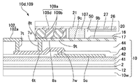
(基板間導通部109等の構成)
図4は、本発明の実施の形態1に係る液晶装置100に用いた第1基板10の平面構成を示す説明図であり、図4(a)、(b)は、電極全体のレイアウトを示す説明図、および第2基板20の角部分の一つを拡大して示す説明図である。なお、図4において画素電極9aやダミー画素電極9bの数等について少なく示してある。図5は、本発明の実施の形態1に係る液晶装置100の断面構成を示す説明図であり、図5(a)、(b)は、端子102と画素電極9aとの電気的な接続構造を模式的に示す説明図、および端子102とダミー画素電極9bとの電気的な接続構造を模式的に示す説明図である。図6は、本発明の実施の形態1に係る液晶装置100における基板間導通材109aによる導通構造を示す説明図である。
(Configuration of
FIG. 4 is an explanatory diagram showing a planar configuration of the
図4に示すように、本形態の液晶装置100において、第1基板10の略中央位置には、複数の画素電極9aが配列された画素領域10aと、画素領域10aとシール材107とにより挟まれた周辺領域10bとが設けられており、周辺領域10bには、第1基板側電極としての複数のダミー画素電極9bが形成されている。複数のダミー画素電極9bにおいて、隣り合うダミー画素電極9b同士は、連結部9uを介して繋がっている。
As shown in FIG. 4, in the
かかる構成のダミー画素電極9b、および第2基板20において第2基板側電極として形成された共通電極21に対する共通電位Vcomの供給は、図2に示す端子102のうち、第1端子102aによって行われ、第2端子102bからはデータ線駆動回路101や走査線駆動回路104に対して各種信号等の入力が行われる。
The supply of the common potential Vcom to the
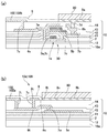
図5(a)に示すように、第2端子102bは、第3層間絶縁膜44の表面に形成されたアルミニウム膜からなり、かかる第2端子102bは、第2層間絶縁膜43の表面等で延在する配線6sに対して、第3層間絶縁膜44に形成されたコンタクトホール7sを介して導通している。ここで、第2端子102bは、画素トランジスター30やデータ線駆動回路の駆動用トランジスター(図5(a)では図示せず)等を介して画素電極9aに電気的に接続している。
As shown in FIG. 5A, the
図4および図5(b)に示すように、第1端子102aは、第2層間絶縁膜43の表面等で延在する配線6tに第3層間絶縁膜44に形成されたコンタクトホール7tを介して導通している。なお、配線6tは、第2層間絶縁膜43に形成されたコンタクトホール7wを介して共通電位線5cに電気的に接続している。
As shown in FIGS. 4 and 5B, the
ここで、第2基板20の4つの角部分10c〜10fには基板間導通部109が形成されている。かかる基板間導通部109では、第3層間絶縁膜44の表面上に、端子102と同時形成されたアルミニウム膜からなる基板間導通用第1電極8tが形成されており、かかる基板間導通用第1電極8tは、第3層間絶縁膜44に形成されたコンタクトホール7uを介して配線6tに導通している。このため、基板間導通用第1電極8tは、第1端子102aに導通し、かつ、第1端子102aと同一種類の導電膜(アルミニウム膜)からなる。
Here,
また、基板間導通部109において、第3層間絶縁膜44の表面上には、ダミー画素電極9bと同時形成されたITO膜からなる延在部9cの先端部に基板間導通用第2電極9tが形成されており、かかる基板間導通用第2電極9tは、ダミー画素電極9bに繋がっている。このため、基板間導通用第2電極9tは、ダミー画素電極9bに導通し、かつ、ダミー画素電極9bと同一種類の導電膜(ITO膜)からなる。ここで、基板間導通用第1電極8tと基板間導通用第2電極9tとは狭いスリット(間隙)8sを介して隣り合っている。
Further, in the
このように、本形態では、基板間導通用第2電極9tおよびダミー画素電極9bは、第1端子102aおよび基板間導通用第1電極8tと異なる種類の導電膜からなる。また、基板間導通用第2電極9tおよびダミー画素電極9bは互いに導通し、第1端子102aおよび基板間導通用第1電極8tは互いに導通している。さらに、基板間導通用第2電極9tおよびダミー画素電極9bを構成する導電膜(ITO膜)と、第1端子102aおよび基板間導通用第1電極8tを構成する導電膜(アルミニウム膜)とは、第1基板10の同じ層間絶縁膜(第3層間絶縁膜44)の表面においてパターンとして分離された状態にある。
Thus, in this embodiment, the
ここで、第1基板10と第2基板20の間には、基板間導通用第1電極8tおよび基板間導通用第2電極9tの双方に跨るように、基板間導通材109aが配置されている。かかる基板間導通材109aは、銀粒子等の導電粒子109bと、樹脂成分109dとからなり、導電粒子109bは、スリット(間隙)8sを跨いで基板間導通用第1電極8tおよび基板間導通用第2電極9tの双方に接している。また、導電粒子109bは、共通電極21にも接している。従って、基板間導通材109aが存在しない状態では層間絶縁膜(第3層間絶縁膜44)の表面において電気的に絶縁された状態にあるが、基板間導通材109aがスリット(間隙)8sを跨いで配置されることによって、基板間導通用第1電極8t、基板間導通用第2電極9t、および共通電極21は、同一の基板間導通材109aによって互いに導通している。なお、図においては模式的に一つの導電粒子109bがスリット(間隙)8sに介在することよって基板間導通用第1電極8t、基板間導通用第2電極9t、および共通電極21を導通させているものとなっているが、スリット(間隙)8sにおいて互いに接続して導通し合う複数の導電粒子が介在する構成であってもよいものである。
Here, between the 1st board |
かかる構成によれば、第1端子102aから供給された共通電位Vcomは、共通電位線5cに印加されるとともに、基板間導通用第1電極8tおよび導電粒子109bを介して、共通電極21に印加される。また、第1端子102aから供給された共通電位Vcomは、基板間導通用第1電極8t、導電粒子109b、および基板間導通用第2電極9tを介してダミー画素電極9bに印加される。さらに、第1端子102aから供給された共通電位Vcomは、基板間導通用第1電極8tおよび導電粒子109bを介して共通電極21に印加された後、共通電極21から導電粒子109bおよび基板間導通用第2電極9tを介してダミー画素電極9bに印加される状態にある。
According to this configuration, the common potential Vcom supplied from the
なお、本形態において、「同一の基板間導通材109a」によって、基板間導通用第1電極8t、基板間導通用第2電極9t、および共通電極21が互いに導通しているとは、図5(b)に示すように、同一の導電粒子109bによって各電極が互いに導通している構成に加えて、図6に示すように、異なる導電粒子109bによって各電極が互いに導通しているが、同一箇所に設けられた基板間導通材109aによって各電極が互いに導通している構成を含む意味である。
In this embodiment, the “inter-substrate conduction
(液晶装置100の製造方法)
図7は、本発明の実施の形態1に係る液晶装置100の製造工程のうち、画素電極9aを形成する工程を示す説明図であり、図7(a)、(b)は、画素領域10aに画素電極9aを形成する工程を示す説明図、および周辺領域10bにダミー画素電極9bを形成する工程を示す説明図である。
(Manufacturing method of the liquid crystal device 100)
FIG. 7 is an explanatory view showing a step of forming the
本形態の液晶装置100を製造するにあたっては、図7(a)、(b)に示すように、周知の半導体プロセスを利用して、画素トランジスター30や各種配線、さらには、端子102を形成した後、画素電極9aやダミー画素電極9bを形成する。より具体的には、第1基板10に対してITO膜9を形成した後、ITO膜9の表面にレジストマスク90を形成し、この状態で、ITO膜9にドライエッチングを行う。しかる後には、第1基板10をアルカリ性あるいは酸性の剥離液と接触させてレジストマスク90を除去する。
In manufacturing the
かかる工程の際、端子102および基板間導通用第1電極8tを構成するアルミニウム膜と、画素電極9a、ダミー画素電極9b、延在部9cおよび基板間導通用第2電極9tを構成するITO膜とは、同一の層間絶縁膜(第3層間絶縁膜44)上にあって露出した状態にある。アルミニウム膜からなる端子102および基板間導通用第1電極8tは剥離液に接するとともに、ITO膜からなる画素電極9a、ダミー画素電極9b、延在部9cおよび基板間導通用第2電極9tも剥離液に接する。
In this process, the aluminum film constituting the terminal 102 and the first
ここで、アルミニウムの標準電極電位は約−1.7Vであるのに対して、ITOの標準電極電位は約−0.2Vであり、アルミニウムは、ITOに比して標準電極電位が低い。従って、アルミニウム膜とITO膜とは導通していると、電気化学的腐食反応(局部電池的な腐食反応)によって、アルミニウム膜が剥離液中に溶出しようとするが、本形態では、アルミニウム膜とITO膜とは低抵抗で導通していないため、アルミニウム膜が溶出しようとする電気化学的腐食反応が発生しない。 Here, the standard electrode potential of aluminum is about −1.7 V, whereas the standard electrode potential of ITO is about −0.2 V, and aluminum has a lower standard electrode potential than ITO. Therefore, when the aluminum film and the ITO film are electrically connected, the aluminum film tends to elute into the stripping solution by the electrochemical corrosion reaction (local battery-like corrosion reaction). Since it is not conductive with the ITO film at a low resistance, the electrochemical corrosion reaction that the aluminum film tends to elute does not occur.
すなわち、図7(b)において、第1端子102aおよび基板間導通用第1電極8tはアルミニウム膜からなる一方、基板間導通用第2電極9tおよびダミー画素電極9bはITO膜からなるが、基板間導通用第1電極8t(アルミニウム膜)と基板間導通用第2電極9t(ITO膜)とは、スリット(間隙)8sによって絶縁分離されており、導通していない。従って、第2端子102bが剥離液中に溶出するような電気化学的腐食反応が発生しない。
That is, in FIG. 7B, the
また、図7(a)に示す第2端子102bは、画素電極9aに電気的に接続しているが、第2端子102bと画素電極9aとは、画素トランジスター30やデータ線駆動回路の駆動用トランジスター等を介して電気的に接続しており、低抵抗で導通している状態にはない。従って、第2端子102bが剥離液中に溶出するような電気化学的腐食反応が発生しない。
7A is electrically connected to the
なお、ITO膜9のパターニングにウエットエッチングを行った場合でも同様なことがいえる。すなわち、ウエットエッチングが進行する過程では、アルミニウム膜からなる端子102および基板間導通用第1電極8tはエッチング液に接するとともに、ITO膜からなる画素電極9a、ダミー画素電極9b、延在部9cおよび基板間導通用第2電極9tもエッチング液に接する。このため、アルミニウム膜とITO膜とが低抵抗で導通していると、電気化学的腐食反応(局部電池的な腐食反応)によって、アルミニウム膜が剥離液中に溶出しようとする。しかるに、本形態では、アルミニウム膜とITO膜とは低抵抗で導通している状態ではないため、アルミニウム膜がエッチング液中に溶出しようとする電気化学的腐食反応が発生しない。
The same applies to the case where wet etching is performed for patterning the ITO film 9. That is, in the process in which the wet etching proceeds, the terminal 102 made of an aluminum film and the first
また、工程順序を変えて、ITO膜によって画素電極9a等を形成した後、アルミニウム膜によって端子102を形成する場合でも、アルミニウム膜とITO膜とが導通していると、電気化学的腐食反応(局部電池的な腐食反応)が発生するが、本形態の構成によれば、アルミニウム膜とITO膜とは低抵抗で導通していないため、アルミニウム膜が溶出しようとする電気化学的腐食反応が発生しない。
In addition, even when the
(本形態の主な効果)
以上説明したように、本形態の液晶装置100において、第1基板10の一方面側には、第1端子102aと、第1端子102aに導通する基板間導通用第1電極8tとが形成されているが、第1端子102aと基板間導通用第1電極8tとは同一種類の導電膜(アルミニウム膜)により構成されている。また、第1基板10の一方面側には、ダミー画素電極9b(第1基板側電極)と、ダミー画素電極9bに導通する基板間導通用第2電極9tとが形成されているが、ダミー画素電極9bと基板間導通用第2電極9tとは同一種類の導電膜(ITO膜)により構成されている。また、第1端子102aおよび基板間導通用第1電極8tを構成するアルミニウム膜と、ダミー画素電極9bおよび基板間導通用第2電極9tを構成するITO膜とは、標準電極電位が異なるが、第1基板10単独の状態では絶縁分離されている。このため、第1基板10に対する製造工程において、レジストマスクの剥離液による剥離や、ウエットエッチング等、電解液を用いたウエットプロセスを行った際、第1端子102a、基板間導通用第1電極8t、ダミー画素電極9b、および基板間導通用第2電極9tが同一の電解液に接触しても、電気化学的腐食反応が発生しない。従って、標準電極電位が低い方の導電膜(アルミニウム膜)が電解液中に溶出するという問題が発生しない。それ故、端子102、基板間導通用第1電極8t、ダミー画素電極9b、および基板間導通用第2電極9tを高い寸法精度や高い形状精度をもって形成することができる。
(Main effects of this form)
As described above, in the
また、第1基板10単独の状態では、第1端子102aおよび基板間導通用第1電極8tを構成する導電膜と、ダミー画素電極9bおよび基板間導通用第2電極9tを構成する導電膜とは絶縁分離されているが、第1基板10と第2基板20との間に基板間導通材109aを設けた際、基板間導通材109aによって、基板間導通用第1電極8t、基板間導通用第2電極9tおよび共通電極21(第2基板側電極)が導通する。それ故、第1端子102aに印加された共通電位Vcomをダミー画素電極9bおよび共通電極21に供給することができる。
In the state of the
また、本形態において、基板間導通用第1電極8tと基板間導通用第2電極9tは、互いに隣り合う位置に設けられ、基板間導通用第1電極8t、基板間導通用第2電極9t、および共通電極21は、同一の基板間導通材109aを介して互いに導通している。このため、狭い領域内において、基板間導通材109aを利用した基板間導通を行うことができる。
In this embodiment, the first
しかも、基板間導通用第1電極8tと基板間導通用第2電極9tは、互いに近接している。このため、基板間導通用第1電極8t、基板間導通用第2電極9t、および共通電極21は、基板間導通材109aに含まれる同一の導電粒子109bに接することになる。それ故、基板間導通用第1電極8t、基板間導通用第2電極9t、および共通電極21を導電粒子109bを介して確実に導通させることができる。
Moreover, the first
[実施の形態2]
図8は、本発明の実施の形態2に係る液晶装置100における端子102とダミー画素電極9bとの電気的な接続構造を模式的に示す説明図である。なお、本形態の基本的な構成は、実施の形態1と同様であるため、共通する部分には、同一の符号を付してそれらの説明を省略する。
[Embodiment 2]
FIG. 8 is an explanatory view schematically showing an electrical connection structure between the terminal 102 and the
図8に示すように、本形態の液晶装置100においても、実施の形態1と同様、基板間導通用第2電極9tおよびダミー画素電極9bを構成する導電膜(ITO膜)と、第1端子102aおよび基板間導通用第1電極8tを構成する導電膜(アルミニウム膜)は絶縁分離された状態にある。従って、第1基板10に対する製造工程において、レジストマスクの剥離液による剥離や、ウエットエッチング等、電解液を用いたウエットプロセスを行った際、第1端子102a、基板間導通用第1電極8t、ダミー画素電極9b、および基板間導通用第2電極9tが同一の電解液に接触しても、電気化学的腐食反応が発生しない。従って、標準電極電位が低い方の導電膜(アルミニウム膜)が電解液中に溶出するという問題が発生しない。
As shown in FIG. 8, in the
また、第1基板10単独の状態では、第1端子102aおよび基板間導通用第1電極8tを構成する導電膜と、ダミー画素電極9bおよび基板間導通用第2電極9tを構成する導電膜とは絶縁分離されているが、本形態では、第1基板10と第2基板20との間では、基板間導通用第1電極8tと重なる位置、および基板間導通用第2電極9tと重なる位置の各々に基板間導通材109aが設けられている。このため、基板間導通用第1電極8tと共通電極21とは基板間導通材109aによって導通し、共通電極21とは基板間導通用第2電極9tとは、別の基板間導通材109aによって導通している。このため、第1端子102aに印加された共通電位Vcomをダミー画素電極9bおよび共通電極21に供給することができる。
In the state of the
[実施の形態3]
図9は、本発明の実施の形態3に係る液晶装置100における端子102とダミー画素電極9b′等との電気的な接続構造を模式的に示す説明図であり、図9(a)、(b)は、角部分10dに設けた基板間導通部等の構成を示す説明図、および角部分10eに設けた基板間導通部等の構成を示す説明図である。なお、本形態の基本的な構成は、実施の形態1と同様であるため、共通する部分には、同一の符号を付してそれらの説明を省略する。
[Embodiment 3]
FIG. 9 is an explanatory diagram schematically showing an electrical connection structure between the terminal 102 and the
本形態では、以下に説明するように、第1基板10上に、上記の第1端子102a、基板間導通用第1電極8t、基板間導通用第2電極9t、第1基板側電極(ダミー画素電極9b)、第2基板側電極(共通電極21)および基板間導通材109aは、印加される電位が異なる複数組が設けられている。
In this embodiment, as described below, the
より具体的には、図9(a)に示すように、本形態の液晶装置100においても、角部分10dでは、実施の形態1と同様、基板間導通用第2電極9tおよびダミー画素電極9bを構成する導電膜(ITO膜)と、第1端子102aおよび基板間導通用第1電極8tを構成する導電膜(アルミニウム膜)は絶縁分離された状態にある。また、第1基板10単独の状態では、第1端子102aおよび基板間導通用第1電極8tを構成する導電膜と、ダミー画素電極9bおよび基板間導通用第2電極9tを構成する導電膜とは絶縁分離されているが、本形態では、角部分10dでは、第1基板10と第2基板20との間において基板間導通用第1電極8tおよび基板間導通用第2電極9tに跨って基板間導通材109aが設けられている。このため、基板間導通用第1電極8tと共通電極21とは基板間導通材109aによって導通し、共通電極21とは基板間導通用第2電極9tとは、別の基板間導通材109aによって導通している。このため、第1端子102aに印加された共通電位Vcomをダミー画素電極9bおよび共通電極21に供給することができる。
More specifically, as shown in FIG. 9 (a), also in the
また、本形態では、図9(b)に示すように、角部分10eでは、第1基板10上に、別の第1端子102a′、別の基板間導通用第1電極8t′、別の基板間導通用第2電極9t′、別の第1基板側電極9b′、別の第2基板側電極21′および別の基板間導通材109a′が設けられており、第1端子102a′には、共通電位Vcom以外の別の電位が印加される。また、第1端子102a′および基板間導通用第1電極8t′は、アルミニウム膜からなる一方、基板間導通用第2電極9t′、および第1基板側電極9b′はITO膜からなる。なお、本形態では、第2基板側電極21′もITO膜からなる。
In this embodiment, as shown in FIG. 9B, at the
ここで、第1基板側電極9b′および第2基板側電極21′は、例えば、ダミー画素電極9bと同時形成されたイオン性不純物除去用の電極からなる。すなわち、液晶注入時に混入したイオン性不純物やシール材から溶出したイオン性不純物が液晶中に存在し、かかるイオン性不純物が液晶駆動に伴って画素領域10aの端部に凝集すると、表示品位の低下を招くが、本形態では、第1基板側電極9b′および第2基板側電極21′に共通電位Vcom以外の別の電位が印加される。このため、ダミー画素電極9bと第1基板側電極9b′との間、共通電極21と第2基板側電極21′との間に横電界が形成されるので、イオン性不純物を引き寄せ、そこで凝集した状態のまま滞留させることができる。それ故、イオン性不純物が画素領域10aに滲み出ないので、イオン性不純物に起因する表示品位の低下を確実に防止することができる。
Here, the first substrate-
かかる構成の液晶装置100においても、第1基板10に対する製造工程において、レジストマスクの剥離液による剥離や、ウエットエッチング等、電解液を用いたウエットプロセスを行った際、第1端子102a′、基板間導通用第1電極8t′、第1基板側電極9b′、および基板間導通用第2電極9t′が同一の電解液に接触しても、電気化学的腐食反応が発生しない。従って、標準電極電位が低い方の導電膜(アルミニウム膜)が電解液中に溶出するという問題が発生しない。
Also in the
[実施の形態1等の改良例]
図10は、本発明の実施の形態1等の改良例に係る液晶装置100における基板間導通部109の平面的な構成を模式的に示す説明図である。
[Improvement example of Embodiment 1 etc.]
FIG. 10 is an explanatory diagram schematically showing a planar configuration of the
実施の形態1等では、基板間導通部109において、基板間導通用第1電極8tおよび基板間導通用第2電極9tはいずれも、スリット(間隙)8sを介して隣り合う矩形形状であった。但し、図10に示す基板間導通用第1電極8tおよび基板間導通用第2電極9tのように、一方側の電極から他方側の電極に向けて突出した凸部が入り込んだ凹部を備えている構成を採用してもよい。より具体的には、基板間導通用第1電極8tは、基板間導通用第2電極9tに向けて突出した複数の凸部81を備えている結果、凸部81の間が凹部82になっている。これに対して、基板間導通用第2電極9tは、基板間導通用第1電極8tの凹部82内に向けて突出した複数の凸部91を備えている結果、凸部91の間は、凸部81が入り込んだ凹部92になっている。また、基板間導通用第1電極8tと基板間導通用第2電極9tとは、スリット(間隙)8sを介して隣り合っている。
In the first embodiment and the like, in the
このような櫛歯形状を採用すれば、1個所に設けられた同一の基板間導通材109aによって基板間導通用第1電極8tと基板間導通用第2電極9tとを導通させる際、基板間導通材109aを設ける位置が多少ずれても、基板間導通用第1電極8tと基板間導通用第2電極9tとを確実に導通させることができる。
When such a comb-teeth shape is employed, when the inter-substrate conducting
[他の実施の形態] [Other embodiments]
上記実施の形態では、画素電極9a等をITO等の透光性導電膜によって形成したが、画素電極9a等をアルミニウムや銀等といった反射性導電膜によって形成し、液晶装置100を反射型として構成してもよい。
In the above embodiment, the
上記実施の形態では、異なる種類の導電膜として、アルミニウムとITOとの組み合わせを説明したが、異なる種類の導電膜として、以下に示す金属等
銀(標準電極電位=+0.80V)
銅(標準電極電位=+0.34V)
ニッケル(標準電極電位=−0.26V)
とITOとの組み合わせ、上記の金属やアルミニウム等とIZO(Indium Zinc Oxide)との組み合わせ、上記の金属やアルミニウム等の金属同士の組み合わせ等を採用した場合に本発明を適用してもよい。また、上記実施の形態では、第1基板側電極がダミー画素電極9bであり、第2基板側電極が共通電極21であったが、一方の電極を形成する際、他方の電極が露出した状態にあれば、第1基板側電極および第2基板側電極が上記以外の電極である場合に本発明を適用してもよい。
In the above embodiment, a combination of aluminum and ITO has been described as a different type of conductive film. However, as a different type of conductive film, the following metals such as silver (standard electrode potential = +0.80 V)
Copper (standard electrode potential = + 0.34V)
Nickel (standard electrode potential = -0.26V)
The present invention may be applied to a case where a combination of ITO and ITO, a combination of the above metals or aluminum and IZO (Indium Zinc Oxide), a combination of metals such as the above metals or aluminum, or the like is employed. In the above embodiment, the first substrate side electrode is the
[電子機器への搭載例]
上述した実施形態に係る液晶装置100を適用した電子機器について説明する。図11は、本発明を適用した液晶装置を用いた投射型表示装置の概略構成図であり、図11(a)、(b)は各々、透過型の液晶装置100を用いた投射型表示装置の説明図、および透過型の液晶装置100を用いた投射型表示装置の説明図である。
[Example of mounting on electronic devices]
An electronic apparatus to which the
(投射型表示装置の第1例)
図11(a)に示す投射型表示装置110は、観察者側に設けられたスクリーン111に光を照射し、このスクリーン111で反射した光を観察する、いわゆる投影型の投射型表示装置である。投射型表示装置110は、光源112を備えた光源部130と、ダイクロイックミラー113、114と、液晶ライトバルブ115〜117(液晶装置100)と、投射光学系118と、クロスダイクロイックプリズム119と、リレー系120とを備えている。
(First example of projection display device)
A
光源112は、赤色光、緑色光及び青色光を含む光を供給する超高圧水銀ランプで構成されている。ダイクロイックミラー113は、光源112からの赤色光を透過させると共に緑色光及び青色光を反射する構成となっている。また、ダイクロイックミラー114は、ダイクロイックミラー113で反射された緑色光及び青色光のうち青色光を透過させると共に緑色光を反射する構成となっている。このように、ダイクロイックミラー113、114は、光源112から出射した光を赤色光と緑色光と青色光とに分離する色分離光学系を構成する。
The
ここで、ダイクロイックミラー113と光源112との間には、インテグレーター121及び偏光変換素子122が光源112から順に配置されている。インテグレーター121は、光源112から照射された光の照度分布を均一化する構成となっている。また、偏光変換素子122は、光源112からの光を例えばs偏光のような特定の振動方向を有する偏光にする構成となっている。
Here, between the
液晶ライトバルブ115は、ダイクロイックミラー113を透過して反射ミラー123で反射した赤色光を画像信号に応じて変調する透過型の液晶装置100である。液晶ライトバルブ115は、λ/2位相差板115a、第1偏光板115b、液晶パネル115c及び第2偏光板115dを備えている。ここで、液晶ライトバルブ115に入射する赤色光は、ダイクロイックミラー113を透過しても光の偏光は変化しないことから、s偏光のままである。
The liquid crystal
λ/2位相差板115aは、液晶ライトバルブ115に入射したs偏光をp偏光に変換する光学素子である。また、第1偏光板115bは、s偏光を遮断してp偏光を透過させる偏光板である。そして、液晶パネル115cは、p偏光を画像信号に応じた変調によってs偏光(中間調であれば円偏光又は楕円偏光)に変換する構成となっている。さらに、第2偏光板115dは、p偏光を遮断してs偏光を透過させる偏光板である。したがって、液晶ライトバルブ115は、画像信号に応じて赤色光を変調し、変調した赤色光をクロスダイクロイックプリズム119に向けて射出する構成となっている。
The λ / 2
なお、λ/2位相差板115a及び第1偏光板115bは、偏光を変換させない透光性のガラス板115eに接した状態で配置されており、λ/2位相差板115a及び第1偏光板115bが発熱によって歪むのを回避することができる。
Note that the λ / 2
液晶ライトバルブ116は、ダイクロイックミラー113で反射した後にダイクロイックミラー114で反射した緑色光を画像信号に応じて変調する透過型の液晶装置100である。そして、液晶ライトバルブ116は、液晶ライトバルブ115と同様に、第1偏光板116b、液晶パネル116c及び第2偏光板116dを備えている。液晶ライトバルブ116に入射する緑色光は、ダイクロイックミラー113、114で反射されて入射するs偏光である。第1偏光板116bは、p偏光を遮断してs偏光を透過させる偏光板である。また、液晶パネル116cは、s偏光を画像信号に応じた変調によってp偏光(中間調であれば円偏光又は楕円偏光)に変換する構成となっている。そして、第2偏光板116dは、s偏光を遮断してp偏光を透過させる偏光板である。したがって、液晶ライトバルブ116は、画像信号に応じて緑色光を変調し、変調した緑色光をクロスダイクロイックプリズム119に向けて射出する構成となっている。
The liquid crystal light valve 116 is a transmissive
液晶ライトバルブ117は、ダイクロイックミラー113で反射し、ダイクロイックミラー114を透過した後でリレー系120を経た青色光を画像信号に応じて変調する透過型の液晶装置100である。そして、液晶ライトバルブ117は、液晶ライトバルブ115、116と同様に、λ/2位相差板117a、第1偏光板117b、液晶パネル117c及び第2偏光板117dを備えている。ここで、液晶ライトバルブ117に入射する青色光は、ダイクロイックミラー113で反射してダイクロイックミラー114を透過した後にリレー系120の後述する2つの反射ミラー125a、125bで反射することから、s偏光となっている。
The liquid crystal
λ/2位相差板117aは、液晶ライトバルブ117に入射したs偏光をp偏光に変換する光学素子である。また、第1偏光板117bは、s偏光を遮断してp偏光を透過させる偏光板である。そして、液晶パネル117cは、p偏光を画像信号に応じた変調によってs偏光(中間調であれば円偏光又は楕円偏光)に変換する構成となっている。さらに、第2偏光板117dは、p偏光を遮断してs偏光を透過させる偏光板である。したがって、液晶ライトバルブ117は、画像信号に応じて青色光を変調し、変調した青色光をクロスダイクロイックプリズム119に向けて射出する構成となっている。なお、λ/2位相差板117a及び第1偏光板117bは、ガラス板117eに接した状態で配置されている。
The λ / 2
リレー系120は、リレーレンズ124a、124bと反射ミラー125a、125bとを備えている。リレーレンズ124a、124bは、青色光の光路が長いことによる光損失を防止するために設けられている。ここで、リレーレンズ124aは、ダイクロイックミラー114と反射ミラー125aとの間に配置されている。また、リレーレンズ124bは、反射ミラー125a、125bの間に配置されている。反射ミラー125aは、ダイクロイックミラー114を透過してリレーレンズ124aから出射した青色光をリレーレンズ124bに向けて反射するように配置されている。また、反射ミラー125bは、リレーレンズ124bから出射した青色光を液晶ライトバルブ117に向けて反射するように配置されている。
The
クロスダイクロイックプリズム119は、2つのダイクロイック膜119a、119bをX字型に直交配置した色合成光学系である。ダイクロイック膜119aは青色光を反射して緑色光を透過する膜であり、ダイクロイック膜119bは赤色光を反射して緑色光を透過する膜である。したがって、クロスダイクロイックプリズム119は、液晶ライトバルブ115〜117のそれぞれで変調された赤色光と緑色光と青色光とを合成し、投射光学系118に向けて射出するように構成されている。
The cross
なお、液晶ライトバルブ115、117からクロスダイクロイックプリズム119に入射する光はs偏光であり、液晶ライトバルブ116からクロスダイクロイックプリズム119に入射する光はp偏光である。このようにクロスダイクロイックプリズム119に入射する光を異なる種類の偏光としていることで、クロスダイクロイックプリズム119において各液晶ライトバルブ115〜117から入射する光を有効に合成できる。ここで、一般に、ダイクロイック膜119a、119bはs偏光の反射特性に優れている。このため、ダイクロイック膜119a、119bで反射される赤色光及び青色光をs偏光とし、ダイクロイック膜119a、119bを透過する緑色光をp偏光としている。投射光学系118は、投影レンズ(図示略)を有しており、クロスダイクロイックプリズム119で合成された光をスクリーン111に投射するように構成されている。
Note that light incident on the cross
(投射型表示装置の第2例)
図11(b)に示す投射型表示装置1000において、光源部890は、システム光軸Lに沿って光源810、インテグレーターレンズ820および偏光変換素子830が配置された偏光照明装置800を有している。また、光源部890は、システム光軸Lに沿って、偏光照明装置800から出射されたS偏光光束をS偏光光束反射面841により反射させる偏光ビームスプリッター840と、偏光ビームスプリッター840のS偏光光束反射面841から反射された光のうち、青色光(B)の成分を分離するダイクロイックミラー842と、青色光が分離された後の光束のうち、赤色光(R)の成分を反射させて分離するダイクロイックミラー843とを有している。
(Second example of projection display device)
In the
また、投射型表示装置1000は、各色光が入射する3つの反射型の液晶装置100(液晶装置100R、100G、100B)を備えており、光源部890は、3つの液晶装置100(液晶装置100R、100G、100B)に所定の色光を供給する。
The
かかる投射型表示装置1000においては、3つの液晶装置100R、100G、100Bにて変調された光をダイクロイックミラー842、843、および偏光ビームスプリッター840にて合成した後、この合成光を投射光学系850によってスクリーン860等の被投射部材に投射する。
In the
(他の投射型表示装置)
なお、投射型表示装置については、光源部として、各色の光を出射するLED光源等を用い、かかるLED光源から出射された色光を各々、別の液晶装置に供給するように構成してもよい。
(Other projection display devices)
In addition, about a projection type display apparatus, you may comprise the LED light source etc. which radiate | emit the light of each color as a light source part, and supply each color light radiate | emitted from this LED light source to another liquid crystal device. .
(他の電子機器)
本発明を適用した液晶装置100については、上記の電子機器の他にも、携帯電話機、情報携帯端末(PDA:Personal Digital Assistants)、デジタルカメラ、液晶テレビ、カーナビゲーション装置、テレビ電話、POS端末、タッチパネルを備えた機器等の電子機器において直視型表示装置として用いてもよい。
(Other electronic devices)
As for the
9a・・画素電極、9b・・ダミー画素電極(第1基板側電極)、9b′・・別の第1基板側電極、8t、8t′・・基板間導通用第1電極、9t、9t′・・基板間導通用第2電極、10・・第1基板、10a・・画素領域、20・・第2基板、21・・共通電極(第2基板側電極)、21′・・別の第2基板側電極、50・・液晶層、109・・基板間導通部、109a・・基板間導通材、110、1000・・投射型表示装置 9a..Pixel electrode, 9b..Dummy pixel electrode (first substrate side electrode), 9b '.. Another first substrate side electrode, 8t, 8t' .. First electrode for inter-substrate conduction, 9t, 9t ' ..Second electrode for inter-substrate conduction, 10 ... First substrate, 10a..Pixel area, 20..Second substrate, 21..Common electrode (second substrate side electrode), 21 '. 2 substrate side electrode, 50 .. liquid crystal layer, 109 .. inter-substrate conducting portion, 109 a .. inter-substrate conducting material, 110, 1000 .. projection type display device
Claims (8)
該第1基板の前記一方面側に対向する面側に第2基板側電極が設けられた第2基板と、
前記第1基板と前記第2基板との間に保持された液晶層と、
前記第1基板の前記一方面側に設けられた端子と、
前記端子と導通し、該端子と同一材料の導電膜で前記第1基板の前記一方面側に形成された基板間導通用第1電極と、
前記端子と異なる材料の導電膜により、前記端子及び前記基板間導通用第1電極と分離して前記第1基板の前記一方面側に形成された第1基板側電極と、
前記第1基板側電極と同一材料の導電膜により、当該第1基板側電極に導通し、前記端子および前記基板間導通用第1電極と分離して前記第1基板の前記一方面側に形成された基板間導通用第2電極と、
前記第1基板と前記第2基板との間に介在することにより、前記第1基板の前記一方面側において分離して形成された前記基板間導通用第1電極と前記基板間導通用第2電極とが導通し、前記基板間導通用第1電極と前記第2基板側電極とが導通し、前記基板間導通用第2電極と前記第2基板側電極とが導通した状態とする基板間導通材と、を有していることを特徴とする液晶装置。 A first substrate provided with a pixel electrode on one side;
A second substrate provided with a second substrate-side electrode on the surface facing the one surface of the first substrate;
A liquid crystal layer held between the first substrate and the second substrate;
Terminals provided on the one surface side of the first substrate;
A first electrode for inter-substrate conduction formed on the one surface side of the first substrate with a conductive film made of the same material as the terminal;
A first substrate side electrode formed on the one surface side of the first substrate separately from the terminal and the first electrode for inter-substrate conduction by a conductive film of a material different from the terminal;
The conductive film made of the same material as that of the first substrate side electrode is electrically connected to the first substrate side electrode, and is formed on the one surface side of the first substrate separately from the terminal and the first electrode for inter-substrate conduction. A second electrode for inter-substrate conduction,
By interposing between the first substrate and the second substrate, the first inter-substrate conduction electrode and the second inter-substrate conduction second formed separately on the one surface side of the first substrate. Between the electrodes, the first electrode for conduction between substrates and the second substrate side electrode are conducted, and the second electrode for conduction between substrates and the second substrate side electrode are conducted. And a conductive material.
前記基板間導通用第1電極、前記基板間導通用第2電極、および前記第2基板側電極は、少なくとも前記間隙に配置された同一の前記基板間導通材を介して互いに導通していることを特徴とする請求項1に記載の液晶装置。 The inter-substrate conduction first electrode and the inter-substrate conduction second electrode are provided at positions adjacent to each other with a gap between them,
The inter-substrate conduction first electrode, the inter-substrate conduction second electrode, and the second substrate-side electrode are electrically connected to each other via at least the same inter-substrate conduction material disposed in the gap. The liquid crystal device according to claim 1.
前記端子および前記基板間導通用第1電極は、当該金属酸化物層より標準電極電位が低い金属層であることを特徴とする請求項1乃至5の何れか一項に記載の液晶装置。 The first substrate side electrode and the second electrode for inter-substrate conduction are conductive metal oxide layers,
6. The liquid crystal device according to claim 1, wherein the terminal and the first electrode for conduction between substrates are metal layers having a standard electrode potential lower than that of the metal oxide layer.
前記液晶装置に供給される光を出射する光源部と、
前記液晶装置によって変調された光を投射する投射光学系と、
を有していることを特徴とする投射型表示装置。 A projection display device comprising the liquid crystal device according to any one of claims 1 to 7,
A light source unit for emitting light supplied to the liquid crystal device;
A projection optical system for projecting light modulated by the liquid crystal device;
A projection display device characterized by comprising:
Priority Applications (2)
| Application Number | Priority Date | Filing Date | Title |
|---|---|---|---|
| JP2010247144A JP2012098577A (en) | 2010-11-04 | 2010-11-04 | Liquid crystal device and projection type display device |
| US13/252,336 US8582069B2 (en) | 2010-11-04 | 2011-10-04 | Liquid crystal device and projection-type display apparatus |
Applications Claiming Priority (1)
| Application Number | Priority Date | Filing Date | Title |
|---|---|---|---|
| JP2010247144A JP2012098577A (en) | 2010-11-04 | 2010-11-04 | Liquid crystal device and projection type display device |
Publications (2)
| Publication Number | Publication Date |
|---|---|
| JP2012098577A true JP2012098577A (en) | 2012-05-24 |
| JP2012098577A5 JP2012098577A5 (en) | 2013-12-05 |
Family
ID=46019318
Family Applications (1)
| Application Number | Title | Priority Date | Filing Date |
|---|---|---|---|
| JP2010247144A Withdrawn JP2012098577A (en) | 2010-11-04 | 2010-11-04 | Liquid crystal device and projection type display device |
Country Status (2)
| Country | Link |
|---|---|
| US (1) | US8582069B2 (en) |
| JP (1) | JP2012098577A (en) |
Cited By (2)
| Publication number | Priority date | Publication date | Assignee | Title |
|---|---|---|---|---|
| WO2014115499A1 (en) * | 2013-01-22 | 2014-07-31 | セイコーエプソン株式会社 | Electro-optic device, electro-optic device manufacturing method, and electronic device |
| WO2016151860A1 (en) * | 2015-03-26 | 2016-09-29 | 堺ディスプレイプロダクト株式会社 | Method for forming contact hole of liquid crystal panel, liquid crystal panel, and liquid crystal display |
Families Citing this family (6)
| Publication number | Priority date | Publication date | Assignee | Title |
|---|---|---|---|---|
| CN103246092B (en) * | 2013-04-28 | 2015-08-19 | 京东方科技集团股份有限公司 | Array base palte and display device |
| KR20150056110A (en) * | 2013-11-14 | 2015-05-26 | 삼성디스플레이 주식회사 | Liquid crystal display device having conductive spacer |
| CN104280954B (en) * | 2014-08-06 | 2017-02-08 | 深圳市华星光电技术有限公司 | Liquid crystal display and lower substrate assembly of liquid crystal display |
| CN104714344A (en) * | 2015-03-31 | 2015-06-17 | 合肥京东方光电科技有限公司 | Blue phase liquid crystal display device and production method thereof |
| CN110098199B (en) * | 2019-05-05 | 2022-04-05 | 深圳市华星光电半导体显示技术有限公司 | Display panel and display device |
| JP2021001966A (en) * | 2019-06-21 | 2021-01-07 | セイコーエプソン株式会社 | Electro-optical device, and electronic apparatus |
Family Cites Families (15)
| Publication number | Priority date | Publication date | Assignee | Title |
|---|---|---|---|---|
| JPH02280374A (en) | 1989-04-21 | 1990-11-16 | Toshiba Corp | Electrode connection in solid-state image sensing device |
| JP3086606B2 (en) * | 1994-11-14 | 2000-09-11 | シャープ株式会社 | Liquid crystal display |
| WO1997034191A1 (en) | 1996-03-14 | 1997-09-18 | Citizen Watch Co., Ltd. | Liquid crystal display device |
| KR100188110B1 (en) * | 1996-04-10 | 1999-06-01 | 김광호 | Lcd device |
| JPH10241861A (en) | 1997-02-21 | 1998-09-11 | Matsushita Electric Ind Co Ltd | Organic light emitting device and display device |
| US5953094A (en) * | 1997-04-04 | 1999-09-14 | Sanyo Electric Co., Ltd. | Liquid crystal display device |
| JP3161528B2 (en) * | 1998-09-07 | 2001-04-25 | 日本電気株式会社 | LCD panel |
| US6335779B1 (en) * | 1999-01-27 | 2002-01-01 | Mistubishi Denki Kaubshiki Kaisha | Liquid crystal display apparatus and method for producing TFT using therefor |
| JP3697173B2 (en) * | 2000-05-25 | 2005-09-21 | セイコーエプソン株式会社 | Liquid crystal device and electronic device |
| JP3702859B2 (en) * | 2001-04-16 | 2005-10-05 | セイコーエプソン株式会社 | Electro-optical device and electronic apparatus |
| JP4050709B2 (en) * | 2003-04-01 | 2008-02-20 | セイコーエプソン株式会社 | Electro-optical device and electronic apparatus including the electro-optical device |
| US7768590B2 (en) * | 2005-04-26 | 2010-08-03 | Sharp Kabushiki Kaisha | Production method of active matrix substrate, active matrix substrate, and liquid crystal display device |
| US7898632B2 (en) * | 2005-12-28 | 2011-03-01 | Seiko Epson Corporation | Electro-optical device, manufacturing method thereof, and electronic apparatus |
| JP2007304384A (en) | 2006-05-12 | 2007-11-22 | Epson Imaging Devices Corp | Liquid crystal device, method for manufacturing the same, and electronic equipment |
| KR101298693B1 (en) * | 2006-07-19 | 2013-08-21 | 삼성디스플레이 주식회사 | Liquid crystal display panel and manufacturing method thereof |
-
2010
- 2010-11-04 JP JP2010247144A patent/JP2012098577A/en not_active Withdrawn
-
2011
- 2011-10-04 US US13/252,336 patent/US8582069B2/en active Active
Cited By (4)
| Publication number | Priority date | Publication date | Assignee | Title |
|---|---|---|---|---|
| WO2014115499A1 (en) * | 2013-01-22 | 2014-07-31 | セイコーエプソン株式会社 | Electro-optic device, electro-optic device manufacturing method, and electronic device |
| JP2014142384A (en) * | 2013-01-22 | 2014-08-07 | Seiko Epson Corp | Electro-optic device, method for manufacturing electro-optic device, and electronic equipment |
| US9645458B2 (en) | 2013-01-22 | 2017-05-09 | Seiko Epson Corporation | Electrooptical device, method of manufacturing electrooptical device, and electronic apparatus |
| WO2016151860A1 (en) * | 2015-03-26 | 2016-09-29 | 堺ディスプレイプロダクト株式会社 | Method for forming contact hole of liquid crystal panel, liquid crystal panel, and liquid crystal display |
Also Published As
| Publication number | Publication date |
|---|---|
| US20120113333A1 (en) | 2012-05-10 |
| US8582069B2 (en) | 2013-11-12 |
Similar Documents
| Publication | Publication Date | Title |
|---|---|---|
| US8786810B2 (en) | Liquid crystal device and electronic apparatus | |
| JP5849489B2 (en) | Electro-optical device, projection display device, electronic apparatus, and method of manufacturing electro-optical device | |
| JP2012098577A (en) | Liquid crystal device and projection type display device | |
| US8953129B2 (en) | Liquid crystal device and projection-type display apparatus | |
| US8817220B2 (en) | Liquid crystal device and projection-type display device | |
| JP5736656B2 (en) | Liquid crystal device and electronic device | |
| JP3199691U (en) | Electro-optical device and electronic apparatus | |
| US10162233B2 (en) | Electro-optical device and electronic apparatus | |
| JP2012083517A (en) | Liquid crystal device and projection display device | |
| JP3199692U (en) | Electro-optical device and electronic apparatus | |
| JP5810589B2 (en) | Electro-optical device, projection display device, and electronic apparatus | |
| JP2009276588A (en) | Electro-optical device and projection type display device | |
| JP6311811B2 (en) | Electro-optical device, projection display device, and electronic apparatus | |
| JP2012185422A (en) | Liquid crystal device, method for manufacturing liquid crystal device and projection type display device | |
| JP2012198386A (en) | Electro-optic device, projection type display device and electronic equipment | |
| JP6107919B2 (en) | Electro-optical device, electronic equipment | |
| JP2012088417A (en) | Method for manufacturing electro-optic device, and electro-optic device | |
| JP5691678B2 (en) | Electro-optic device, projection display device | |
| JP2012208294A (en) | Method for manufacturing electro-optic device, electro-optic device, projection-type display device, and electronic equipment | |
| JP2012198255A (en) | Substrate and manufacturing method of electro-optical device | |
| JP5332841B2 (en) | Electro-optical device and electronic apparatus | |
| JP2013109258A (en) | Electro-optic device and electronic apparatus | |
| JP2012185423A (en) | Electro-optic device and projection display | |
| JP2012189758A (en) | Method for manufacturing electro-optic device | |
| JP2012123141A (en) | Electro-optical device, manufacturing method for electro-optical device, and projection type display device |
Legal Events
| Date | Code | Title | Description |
|---|---|---|---|
| A521 | Written amendment |
Free format text: JAPANESE INTERMEDIATE CODE: A523 Effective date: 20131018 |
|
| A621 | Written request for application examination |
Free format text: JAPANESE INTERMEDIATE CODE: A621 Effective date: 20131018 |
|
| A761 | Written withdrawal of application |
Free format text: JAPANESE INTERMEDIATE CODE: A761 Effective date: 20131216 |