JP2012064803A - Surface detecting device, exposure device, surface detecting method, exposure method, and device manufacturing method - Google Patents
Surface detecting device, exposure device, surface detecting method, exposure method, and device manufacturing method Download PDFInfo
- Publication number
- JP2012064803A JP2012064803A JP2010208375A JP2010208375A JP2012064803A JP 2012064803 A JP2012064803 A JP 2012064803A JP 2010208375 A JP2010208375 A JP 2010208375A JP 2010208375 A JP2010208375 A JP 2010208375A JP 2012064803 A JP2012064803 A JP 2012064803A
- Authority
- JP
- Japan
- Prior art keywords
- detection
- fluid
- substrate
- surface detection
- outlet
- Prior art date
- Legal status (The legal status is an assumption and is not a legal conclusion. Google has not performed a legal analysis and makes no representation as to the accuracy of the status listed.)
- Pending
Links
Images


Abstract
Description
本発明は、表面検出装置、露光装置、表面検出方法、露光方法、及びデバイス製造方法に関する。 The present invention relates to a surface detection apparatus, an exposure apparatus, a surface detection method, an exposure method, and a device manufacturing method.
露光装置は、デバイスの製造過程等におけるフォトリソグラフィ工程で使用されている。露光装置は、例えば露光対象の基板の表面(段差、うねり、凹凸)等の検出結果に基づいて、基板の表面に焦点を合わせた状態で、この基板を露光する。基板の表面の検出には、例えば位相差方式やコントラスト方式のオートフォーカス機構等を利用した光学的な検出装置が用いられる。光学的な検出装置は、例えば基板の表面に検出光を照射し、基板の表面で反射した検出光を検出する。また、流体を利用して基板の表面を検出可能な流体ゲージセンサーが、下記の特許文献1に開示されている。 The exposure apparatus is used in a photolithography process in a device manufacturing process or the like. The exposure apparatus exposes the substrate in a state of focusing on the surface of the substrate, for example, based on the detection result of the surface (step, swell, unevenness) of the substrate to be exposed. For the detection of the surface of the substrate, for example, an optical detection device using a phase difference type or contrast type autofocus mechanism is used. The optical detection device irradiates the surface of the substrate with detection light, for example, and detects the detection light reflected on the surface of the substrate. Further, a fluid gauge sensor capable of detecting the surface of a substrate using a fluid is disclosed in Patent Document 1 below.
上述の光学的な検出装置を利用して検出対象面を検出すると、検出対象面の光学特性によって検出精度が低下する可能性がある。例えば、露光対象面に、配線や電極等の導電膜、保護膜や反射防止膜等の絶縁膜、スイッチング素子等の一部を構成する半導体膜が形成されていると、検出光に対するこれら各種膜の反射率や透過率、屈折率の違いによって、検出精度が影響を受ける可能性がある。例えば、各種膜の界面が基板の表面として検出される可能性がある。 When the detection target surface is detected using the above-described optical detection device, the detection accuracy may be reduced due to the optical characteristics of the detection target surface. For example, when a conductive film such as a wiring or an electrode, an insulating film such as a protective film or an antireflection film, or a semiconductor film constituting a part of a switching element is formed on the exposure target surface, these various films against the detection light Detection accuracy may be affected by differences in reflectance, transmittance, and refractive index. For example, the interface between various films may be detected as the surface of the substrate.
本発明は、上述の事情に鑑み成されたものであって、検出対象面の光学特性に依らずに検出対象面を検出可能にすることを目的の1つとする。 The present invention has been made in view of the above circumstances, and an object thereof is to enable detection of a detection target surface without depending on the optical characteristics of the detection target surface.
本発明の第1の態様である表面検出装置は、流体の吹出口を有する第1部材と、前記第1部材と検出対象面との間に配置され、前記吹出口からの流体の少なくとも一部が流入する流入口、及び前記流入口を通った流体が前記検出対象面に向けて流出する流出口を有する第2部材と、前記流出口から流出する流体の流れ方向における前記第2部材の位置を検出する検出部と、を備える。 The surface detection device according to the first aspect of the present invention includes a first member having a fluid outlet, and is disposed between the first member and the detection target surface, and at least a part of the fluid from the outlet. A second member having an inflow port through which the fluid flows, and an outflow port through which the fluid passing through the inflow port flows out toward the detection target surface, and the position of the second member in the flow direction of the fluid flowing out from the outflow port And a detecting unit for detecting.
本発明の第2の態様である露光装置は、本発明の態様の表面検出装置を備える。 An exposure apparatus according to a second aspect of the present invention includes the surface detection apparatus according to the aspect of the present invention.
本発明の第3の態様であるデバイス製造方法は、本発明の態様の露光装置を用いて基板を露光することと、露光された前記基板を現像することと、を含む。 A device manufacturing method according to a third aspect of the present invention includes exposing a substrate using the exposure apparatus according to the aspect of the present invention, and developing the exposed substrate.
本発明の第4の態様である表面検出方法は、流体の流入口、及び前記流入口を通った流体が流出する流出口を有する部材を、前記流出口を検出対象面に向けて配置することと、前記流入口に流体を供給することと、前記流出口から流出した流体から前記部材が受ける力によって、前記検出対象面から前記部材を離すことと、前記流入口に流体が供給されている状態で、前記流出口から流出する流体の流れ方向における前記部材の位置を検出することと、を含む。 In the surface detection method according to the fourth aspect of the present invention, a member having a fluid inlet and an outlet from which the fluid flows out through the inlet is disposed with the outlet facing the detection target surface. Supplying the fluid to the inlet, separating the member from the detection target surface by the force received by the member from the fluid flowing out from the outlet, and supplying the fluid to the inlet And detecting the position of the member in the flow direction of the fluid flowing out from the outlet.
本発明の第5の態様である露光方法は、本発明の態様の表面検出方法を用いて基板の表面を検出することと、前記基板の表面に光を照射して前記基板の表面を検出することと、前記表面検出方法による検出結果と前記光による検出結果とを比較することと、前記比較の結果に基づいて前記基板を露光することと、を含む。 An exposure method according to a fifth aspect of the present invention detects the surface of the substrate using the surface detection method according to the aspect of the present invention, and detects the surface of the substrate by irradiating the surface of the substrate with light. And comparing the detection result by the surface detection method with the detection result by the light, and exposing the substrate based on the comparison result.
本発明の第6の態様であるデバイス製造方法は、本発明の態様の露光方法を用いて基板を露光することと、露光された前記基板を現像することと、を含む。 A device manufacturing method according to a sixth aspect of the present invention includes exposing a substrate using the exposure method according to the aspect of the present invention and developing the exposed substrate.
本発明によれば、検出対象面の光学特性に依らずに検出対象の表面を検出することが期待できる。 According to the present invention, it can be expected to detect the surface of the detection target regardless of the optical characteristics of the detection target surface.
<第1実施形態>
以下、本発明の実施形態について図面を参照しながら説明するが、本発明はこれに限定されない。以下の説明では、XYZ直交座標系を参照しつつ各部の位置関係について説明する。このXYZ直交座標系において、水平面内の所定方向をX軸方向、水平面内においてX軸方向と直交する方向をY軸方向、X軸方向及びY軸方向のそれぞれと直交する方向(すなわち鉛直方向)をZ軸方向とする。X軸、Y軸、及びZ軸まわりの回転(傾斜)方向をそれぞれ、θX、θY、及びθZ方向とする。
<First Embodiment>
Hereinafter, embodiments of the present invention will be described with reference to the drawings, but the present invention is not limited thereto. In the following description, the positional relationship of each part will be described with reference to an XYZ orthogonal coordinate system. In this XYZ orthogonal coordinate system, a predetermined direction in the horizontal plane is the X-axis direction, and a direction orthogonal to the X-axis direction in the horizontal plane is a direction orthogonal to the Y-axis direction, the X-axis direction, and the Y-axis direction (that is, the vertical direction). Is the Z-axis direction. The rotation (tilt) directions around the X axis, Y axis, and Z axis are the θX, θY, and θZ directions, respectively.
図1は、第1実施形態のデバイス製造システムの一例を示す図である。本例のデバイス製造システムSYSは、コータデベロッパ装置CD、露光装置EX、及びインターフェース部IFを含む。デバイス製造システムSYSは、デバイス製造用の基板Pに各種処理を行う。デバイス製造用の基板Pには、必要に応じて、図示略の成膜装置等によってデバイスを構成する膜が形成される。この膜は、例えば、配線や電極となる導電膜、各種ダイオードの半導体層となる半導体膜、保護膜や誘電体となる絶縁膜等である。 FIG. 1 is a diagram illustrating an example of a device manufacturing system according to the first embodiment. The device manufacturing system SYS of this example includes a coater / developer apparatus CD, an exposure apparatus EX, and an interface unit IF. The device manufacturing system SYS performs various processes on the device manufacturing substrate P. A film constituting the device is formed on the substrate P for device manufacture by a film forming apparatus (not shown) or the like as necessary. This film is, for example, a conductive film to be a wiring or an electrode, a semiconductor film to be a semiconductor layer of various diodes, an insulating film to be a protective film or a dielectric.
本例のデバイス製造システムSYSは、概略すると以下のように動作する。コータデベロッパ装置CDは、デバイス製造用の基板Pに感光材(フォトレジスト)の膜を形成する。本例のインターフェース部IFは、ロードロック機構を含み、コータデベロッパ装置CDと露光装置EXとを接続している。感光材の膜が形成された基板Pは、インターフェース部IFを介して露光装置EXに搬送される。露光装置EXは、基板Pにパターンを露光する。露光された基板Pは、インターフェース部IFを介してコータデベロッパ装置CDに搬送される。コータデベロッパ装置CDは、露光処理後の基板Pを現像する。現像処理後の基板Pは、必要に応じて、図示略のエッチング装置等によってエッチングされる。 The device manufacturing system SYS of this example generally operates as follows. The coater / developer apparatus CD forms a film of a photosensitive material (photoresist) on a substrate P for device manufacture. The interface unit IF of this example includes a load lock mechanism, and connects the coater / developer apparatus CD and the exposure apparatus EX. The substrate P on which the photosensitive material film is formed is transported to the exposure apparatus EX via the interface unit IF. The exposure apparatus EX exposes a pattern on the substrate P. The exposed substrate P is transported to the coater / developer apparatus CD via the interface unit IF. The coater / developer apparatus CD develops the substrate P after the exposure processing. The substrate P after the development processing is etched by an etching apparatus (not shown) or the like as necessary.
次に、デバイス製造システムSYSの構成要素について説明する。本例の露光装置EXは、液浸露光装置である。本発明は、液浸露光以外の露光装置にも適用可能である。本例の露光装置EXは、マスクステージ1、基板ステージ2、照明光学系IL、投影光学系PL、液浸部材3、制御装置4、記憶装置5、第1干渉計6、第2干渉計7、第1搬送装置8、表面検出装置9、及び第1チャンバ装置CH1を含む。
Next, components of the device manufacturing system SYS will be described. The exposure apparatus EX of this example is an immersion exposure apparatus. The present invention is also applicable to exposure apparatuses other than immersion exposure. The exposure apparatus EX of this example includes a mask stage 1, a
マスクステージ1は、マスクMを保持して移動可能である。第1干渉計6は、マスクステージ1の位置を計測する。照明光学系ILは、マスクMを露光光ELで照明する。第1搬送装置8は、インターフェース部IFと基板ステージ2との間で基板Pを搬送する。表面検出装置9は、基板Pの表面等を検出する。基板ステージ2は、基板Pを保持して移動可能である。第2干渉計7は、基板ステージ2の位置を計測する。液浸部材3は、基板Pに照射される露光光ELの光路が液体LQ1で満たされるように基板Pとの間で液体LQ1を保持して、液浸空間を形成する。投影光学系PLは、露光光ELで照明されたマスクMのパターンの像を基板Pに投影する。制御装置4は、記憶装置5に記憶されているプログラムやデータに基づいて、露光装置EXを制御する。
The mask stage 1 is movable while holding the mask M. The first interferometer 6 measures the position of the mask stage 1. The illumination optical system IL illuminates the mask M with the exposure light EL. The first transport device 8 transports the substrate P between the interface unit IF and the
マスクステージ1は、マスクMを保持した状態で、照明領域を含む領域を移動可能である。マスクMは、基板Pに投影されるデバイスパターンが形成されたレチクルを含む。本例のマスクMは、透過型マスクを含む。この透過型マスクは、例えば、ガラス板等の透明板と、その透明板上にクロム等の遮光材料を用いて形成されたパターンとを有する。マスクステージ1は、例えば米国特許第6452292号明細書に開示されているような平面モータを含む駆動システムの作動により、X軸、Y軸、Z軸、θX、θY、及びθZ方向の6つの方向に移動可能である。 The mask stage 1 can move in the area including the illumination area while holding the mask M. The mask M includes a reticle on which a device pattern projected onto the substrate P is formed. The mask M in this example includes a transmissive mask. This transmissive mask has, for example, a transparent plate such as a glass plate and a pattern formed on the transparent plate using a light shielding material such as chromium. The mask stage 1 has six directions of X axis, Y axis, Z axis, θX, θY, and θZ directions by operation of a drive system including a planar motor as disclosed in, for example, US Pat. No. 6,452,292. Can be moved to.
基板ステージ2は、基板Pを保持した状態で、投影領域を含む領域を移動可能である。本例の基板ステージ2は、マスクステージ1と同様の駆動システムの作動により、X軸、Y軸、Z軸、θX、θY、及びθZ方向の6つの方向に移動可能である。基板ステージ2を移動させる駆動システムは、平面モータでなくてもよい。
The
本例の基板ステージ2は、例えば米国特許出願公開第2007/0177125号明細書、及び米国特許出願公開第2008/0049209号明細書等に開示されているような、カバー部材をリリース可能に保持するカバー部材保持部を含む。本例の基板ステージ2の上面は、カバー部材保持部に保持されたカバー部材の上面を含む。基板ステージ2の上面が、基板ステージ2に搭載されているセンサ、計測部材等の表面を含んでもよい。
The
本例の基板ステージ2は、基板Pをリリース可能に保持する基板保持部を含む。基板保持部は、基板Pの表面が+Z方向を向くように基板Pを保持する。本例では、基板保持部に保持された基板Pの表面と、その基板Pの周囲に配置される基板ステージ2の上面とは、ほぼ同一平面内に配置される(面一である)。
The
照明光学系ILは、所定の照明領域に露光光ELを照射する。照明光学系ILは、照明領域に配置されたマスクMの少なくとも一部を均一な照度分布の露光光ELで照明する。照明光学系ILから射出される露光光ELとして、例えば水銀ランプから射出される輝線(g線、h線、i線)及びKrFエキシマレーザ光(波長248nm)等の遠紫外光(DUV光)、ArFエキシマレーザ光(波長193nm)、及びF2レーザ光(波長157nm)等の真空紫外光(VUV光)等が用いられる。本例では、露光光ELとして、紫外光(真空紫外光)であるArFエキシマレーザ光を用いる。 The illumination optical system IL irradiates a predetermined illumination area with the exposure light EL. The illumination optical system IL illuminates at least a part of the mask M arranged in the illumination area with the exposure light EL having a uniform illuminance distribution. As the exposure light EL emitted from the illumination optical system IL, for example, far ultraviolet light (DUV light) such as a bright line (g line, h line, i line) and KrF excimer laser light (wavelength 248 nm) emitted from a mercury lamp, ArF excimer laser light (wavelength 193 nm), vacuum ultraviolet light (VUV light) such as F 2 laser light (wavelength 157 nm), or the like is used. In this example, ArF excimer laser light, which is ultraviolet light (vacuum ultraviolet light), is used as the exposure light EL.
投影光学系PLは、所定の投影領域に露光光ELを照射する。本例の露光装置EXは、図示略の合焦装置を含んでいる。この合焦装置は、検出光を基板Pに照射して基板Pの表面(露光対象面)を検出し、投影光学系PLの焦点を露光対象面に合わせることが可能である。投影光学系PLは、投影領域に配置された基板Pの少なくとも一部に、マスクMのパターンの像を所定の投影倍率で投影する。投影光学系PLは、縮小系、等倍系、及び拡大系のいずれでもよい。本例の投影光学系PLの光軸AXは、Z軸と平行である。投影光学系PLは、投影光学系PLの像面に向けて露光光ELを射出する射出面を有する。投影光学系PLは、反射光学素子を含まない屈折系、屈折光学素子を含まない反射系、反射光学素子と屈折光学素子とを含む反射屈折系のいずれでもよい。投影光学系PLは、倒立像と正立像のいずれを形成してもよい。 The projection optical system PL irradiates a predetermined projection area with the exposure light EL. The exposure apparatus EX of this example includes a focusing device (not shown). This focusing device can irradiate the detection light onto the substrate P to detect the surface (exposure target surface) of the substrate P and focus the projection optical system PL on the exposure target surface. The projection optical system PL projects an image of the pattern of the mask M at a predetermined projection magnification onto at least a part of the substrate P arranged in the projection area. Projection optical system PL may be any one of a reduction system, a unity magnification system, and an enlargement system. The optical axis AX of the projection optical system PL of this example is parallel to the Z axis. Projection optical system PL has an exit surface that emits exposure light EL toward the image plane of projection optical system PL. Projection optical system PL may be any of a refractive system that does not include a reflective optical element, a reflective system that does not include a refractive optical element, or a catadioptric system that includes a reflective optical element and a refractive optical element. Projection optical system PL may form either an inverted image or an erect image.
第1干渉計6は、マスクステージ1に配置された計測ミラーを用いて、レーザ光の干渉によりマスクステージ1の位置を計測可能である。第2干渉計7は、基板ステージ2に配置された計測ミラーを用いて、レーザ光の干渉により基板ステージ2の位置を計測可能である。基板Pの露光処理、あるいは所定の計測処理を実行するとき、制御装置4は、第1干渉計6及び第2干渉計7の計測結果に基づいて、マスクステージ1(マスクM)及び基板ステージ2(基板P)の位置制御を実行する。
The first interferometer 6 can measure the position of the mask stage 1 by laser beam interference using a measurement mirror arranged on the mask stage 1. The
本例の露光装置EXは、マスクMと基板Pとを所定の走査方向に同期移動しつつ、マスクMのパターンの像を基板Pに投影する走査型露光装置(所謂スキャニングステッパ)である。本例では、基板Pの走査方向(同期移動方向)をY軸方向とし、マスクMの走査方向(同期移動方向)もY軸方向とする。制御装置4は、基板Pを投影光学系PLの投影領域に対してY軸方向に移動するとともに、その基板PのY軸方向への移動と同期して、照明光学系ILの照明領域に対してマスクMをY軸方向に移動しつつ、投影光学系PLと基板P上の液浸空間の液体LQ1とを介して基板Pに露光光ELを照射する。 The exposure apparatus EX of this example is a scanning exposure apparatus (so-called scanning stepper) that projects an image of the pattern of the mask M onto the substrate P while synchronously moving the mask M and the substrate P in a predetermined scanning direction. In this example, the scanning direction (synchronous movement direction) of the substrate P is the Y-axis direction, and the scanning direction (synchronous movement direction) of the mask M is also the Y-axis direction. The control device 4 moves the substrate P in the Y-axis direction with respect to the projection area of the projection optical system PL, and synchronizes the movement of the substrate P in the Y-axis direction with respect to the illumination area of the illumination optical system IL. Then, the substrate P is irradiated with the exposure light EL through the projection optical system PL and the liquid LQ1 in the immersion space on the substrate P while moving the mask M in the Y-axis direction.
液浸部材3は、投影領域に照射される露光光ELの光路が液体LQ1で満たされるように液浸空間を形成する。液浸部材3は、投影光学系PLの射出面と、射出面から射出される露光光ELを照射可能な位置に配置される物体との間の露光光ELの光路が液体LQ1で満たされるように、物体との間で液体LQ1を保持して液浸空間を形成する。 The liquid immersion member 3 forms a liquid immersion space so that the optical path of the exposure light EL irradiated to the projection area is filled with the liquid LQ1. The liquid immersion member 3 is configured so that the optical path of the exposure light EL between the exit surface of the projection optical system PL and the object disposed at a position where the exposure light EL emitted from the exit surface can be irradiated is filled with the liquid LQ1. In addition, the liquid LQ1 is held between the object and an immersion space is formed.
制御装置4は、露光装置EX全体の動作を制御する。記憶装置5は、制御装置4に接続されており、露光に関する各種の情報を記憶する。制御装置4及び記憶装置5は、例えばコンピュータシステムの一部又は全部である。記憶装置5は、例えばRAM等のメモリ、ハードディスク、CD−ROM等の記録媒体を含む。記憶装置5には、コンピュータシステムを制御するオペレーティングシステム(OS)がインストールされ、露光装置EXを制御するためのプログラムが記憶されている。 The control device 4 controls the overall operation of the exposure apparatus EX. The storage device 5 is connected to the control device 4 and stores various types of information related to exposure. The control device 4 and the storage device 5 are, for example, part or all of a computer system. The storage device 5 includes a memory such as a RAM, and a recording medium such as a hard disk and a CD-ROM. The storage device 5 is installed with an operating system (OS) for controlling the computer system, and stores a program for controlling the exposure apparatus EX.
第1搬送装置8は、露光処理前の基板Pを、露光装置EXの基板ステージ2に搬入(ロード)する。第1搬送装置8は、露光処理後の基板Pを露光装置EXの基板ステージ2から搬出(アンロード)する。
The first transport device 8 loads (loads) the substrate P before the exposure processing onto the
本例の表面検出装置9は、本発明を適用した装置である。本例の表面検出装置9は、第1搬送装置8の搬送経路に配置されている。本例の表面検出装置9は、第1搬送装置8の搬送経路に対して固定されている。表面検出装置9は、その構成を後述するが、基板Pの光学特性に依らずに基板Pの表面を検出可能である。本例の制御装置4は、上述の合焦装置による基板Pの表面の検出結果と、表面検出装置9の検出結果とを比較して合焦の成否を判定する。本例の制御装置4は、合焦の成否の判定結果に基づいて、合焦装置を制御する。なお、基板ステージ1とインターフェース部IFとの間の搬送経路に、計測ステージが配置されていてもよい。計測ステージに、基板Pの表面を光学的に検出する検出装置が配置されていてもよい。この検出装置は、基板Pに検出光を照射し、基板Pを経由した光を検出する装置であってもよい。この検出装置の結果と、表面検出装置9の検出結果とを併用して、基板Pの表面を検出してもよい。
The
第1チャンバ装置CH1は、少なくとも投影光学系PL、液浸部材3、及び基板ステージ2が配置される内部空間を形成する。第1チャンバ装置CH1は、内部空間の環境(温度、湿度、圧力、及びクリーン度)を制御する環境制御装置を含む。
The first chamber apparatus CH1 forms an internal space in which at least the projection optical system PL, the liquid immersion member 3, and the
コータデベロッパ装置CDは、装置本体10、浸漬装置11、温度調整装置12、第2搬送装置13、及び第2チャンバ装置CH2を含む。第2チャンバ装置CH2は、第1チャンバ装置CH1と同様の装置であり、第1チャンバとは別の内部空間を形成する。装置本体10は、第2チャンバ装置CH2の内部空間に配置されている。第2搬送装置13は、装置本体10とインターフェース部IFとの間で基板Pを搬送する。装置本体10は、塗布装置及び現像装置を含む。この塗布装置は、露光処理前の基板Pに対して感光材(レジスト)を塗布する。現像装置は、露光処理後の基板Pを現像処理する。浸漬装置11及び温度調整装置12は、第2搬送装置13の搬送経路に配置されている。浸漬装置11は、基板Pを第2液体LQ2に浸漬する。温度調整装置12は、基板Pの温度調整を行う。
The coater / developer apparatus CD includes an apparatus
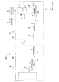
図2は、第1実施形態に係る表面検出装置の一例を示す図である。図2(a)は、表面検出装置9を下方(−Z側)から見た平面図に相当し、図2(b)は、図2(a)のA−A’線断面図に相当する。
FIG. 2 is a diagram illustrating an example of the surface detection apparatus according to the first embodiment. 2A corresponds to a plan view of the
本例の表面検出装置9は、第1部材20、第2部材21、第3部材22、及び検出部23を含む。表面検出装置9により基板P(検出対象物)の表面(検出対象面)を検出するとき(以下、検出動作時という)に、第1部材20は、検出対象面から+Z側に離れた位置に配置される。第1部材20は、流体Gの吹出口24を有する。検出動作時に、第2部材21は、第1部材20と基板Pとの間に配置される。第2部材21は、吹出口24からの流体Gの少なくとも一部が流入する流入口27、及び流入口27を通った流体Gが検出対象面に向かって流出する流出口28を有する。第3部材22は、第1部材20からと第2部材21までの最大距離を規制する。検出部23は、流出口28から流出する流体Gの流れ方向(Z方向)における第2部材21の位置を検出する。
The
本例の第1部材20は、吹出口24に通じる内部流路25を有する。内部流路25は、流体Gを供給可能な供給部(以下、流体供給部GSという)に接続される。本例の内部流路25は、吹出口24に向うにつれて、内寸(内径)が縮小するノズル形状を含む。本例の流体Gは、窒素ガス等の不活性ガスである。流体Gは、気相、液相、液相及び気相の混相のいずれでもよい。本例の露光装置EXは、流体供給部GSを含んでいる。流体供給部GSの一部又は全部が、露光装置EXの外部装置であっても構わない。
The
本例の第1部材20は、円板状の部材を含む。本例の第1部材20は、検出動作時の基板Pを向けて配置される下面26を有する。第2部材21は、第1部材20の下面26の少なくとも一部と対向するように配置される。本例の下面26は、第2部材21と対向する領域が、実質的に平面である。下面26は、第2部材21に向って凸形状となる曲面と第2部材21に向って凹形状となる曲面の少なくとも一方を含んでもよい。吹出口24は、下面26に配置されている。流体供給部GSから供給された流体Gは、内部流路25を通って吹出口24から第1部材20の外部に吹出される。本例では、吹出口24から吹出された流体Gの少なくとも一部が、−Z側に向かって流れる。
The
本例の第2部材21は、円板状の部材を含む。第2部材21の外寸(直径)は、例えば10μm以上10mm以下であり、25μm以上4mm以下、あるいは50μm以上2mm以下であってもよい。本例の第2部材21は、第1面(以下、上面30という)と、第1面とは異なる方向を向く第2面(以下、下面31という)とを有する。本例の第2部材21は、上面30と下面31とを結ぶ孔(openingsまたはpores)29を有する。本例の孔29は、貫通孔であり、その一方の開口が流入口27、他方の開口が流出口28である。本例では、流入口27と流出口28とを結ぶ線が、Z方向に平行である。
The
本例の孔29は、上面30から下面31に向かう方向で、内寸(内径)が実質的に変化しないストレートな貫通孔である。孔29は、上面30と下面31の一方から他方に向かう方向に、内寸(内径)が縮小するテーパ形状でもよい。例えば、孔29は、上面30から下面31に向かうにつれて、内寸(内径)が縮小するノズル形状を含んでいてもよい。
The
第2部材21は、複数の孔29を有していてもよい。第2部材21は、網目状に多数の孔(気孔、pores)が形成された多孔部材(ポーラス部材)を含んでいてもよい。第2部材21の上面30を含む部分が孔(openings)を含む部材であり、第2部材21のうちの下面31を含む部分が多孔部材であってもよい。
The
第2部材21の上面30は、第1部材20の下面26に対向して配置される。本例の上面30は、実質的に平面である。上面30は、第1部材20に向って凸形状となる曲面と第1部材20に向って凹形状となる曲面の少なくとも一方を含んでもよい。流入口27は、上面30に配置されている。検出動作時に、Z方向から平面視した状態で吹出口24の少なくとも一部が流入口27と重なるように、第2部材21が配置される。第2部材21の下面31は、基板Pの表面に対向して配置される。本例の下面31は、実質的に平面である。下面31は、基板Pの表面に向って凸形状となる曲面と基板Pの表面に向って凹形状となる曲面の少なくとも一方を含んでもよい。流出口28は、下面31に配置されている。すなわち、検出動作時に、流出口28が基板Pの表面を向くように、第2部材21が配置される。
The
本例の第2部材21は、孔29の周縁部と比較して薄厚の外縁部32を含む。本例では、孔29の周縁部が外縁部32よりも−Z側に突出している。本例では、外縁部32が第3部材22に支持される。
The
本例の第3部材22は、第1部材20の下面26と接続されている。本例では、第2部材21を囲むように、複数の第3部材22が配置されている。本例の第3部材22は、第1部材20から−Z側に突出して、XY面に沿う方向に折れ曲がっている。本例の第3部材22は、Z方向を含む断面がL字形状である。表面検出装置9と基板Pとが対向していない状態、あるいは吹出口24から流体Gが吹出されていない状態で、第3部材22においてXY面に沿う方向に延びる部分に、第2部材21の外縁部32が載置(支持)される。第2部材21は、その外縁部32が第3部材22よりも基板P側に移動することが抑制されている。本例では、第2部材21が第3部材22に支持されている状態で、第3部材22が第2部材21よりも基板P側に突出しないように、外縁部32の板厚が設定されている。
The
なお、第3部材22は、圧縮力に対する変形量が引張力に対する変形量よりも十分に大きい部材、例えば糸状の部材等であってもよい。第3部材22が糸状の部材であって、この部材の一端側が第2部材21に接続されているとともに、他端側が第1部材20又は他の部材に接続されており、第3部材22を介して第2部材21が支持されていてもよい。
The
本例の検出部23は、少なくとも検出動作時に、表面検出装置9と基板Pと対向する方向の位置が固定される。本例の検出部23は、第1部材20に埋め込まれている。本例の第1部材20は、少なくとも検出動作時に、表面検出装置9と基板Pと対向する方向の位置が固定される。検出部23は、流出口28から流出する流体Gの流れ方向(Z方向)における第2部材21の位置を検出可能である。本例の検出部23は、第1部材20に対する相対位置が固定されており、実質的に第1部材20に対する第2部材21の位置を検出する。本例では、吹出口24を囲むように、複数の検出部23が配置されている。
In the
本例の検出部23は、第2部材21の上面30に検出光を照射し、上面30で反射した検出光を検出することによって、検出部23(第1部材20)から第2部材21の上面30までの距離を検出する。本例の検出部23は、干渉計を含む。本例の検出部23は、上記の検出光としてレーザ光を照射し、上面30で反射したレーザ光の干渉を用いて、検出部23から上面30までの距離を測定する。第2部材21において、少なくとも検出部23からレーザ光が入射する領域は、このレーザ光に対する光学特性が既知である材質に設定される。上記の光学特性は、透過率、反射率、吸収率、及び屈折率のうちの1以上を含む。
The
なお、第2部材21の上面30に、第2部材21上での位置を示す識別子等が設けられていてもよい。検出部23は、この識別子に照射されたレーザ光を検出してもよい。検出部23は、第2部材21との間の静電容量を検出する静電容量計を含んでいてもよい。第2部材21が磁石等の磁力発生源を含み、検出部23が第2部材21との間の磁界を検出してもよい。第2部材21の物理特性は、検出部23の検出原理に応じて、適宜選択される。
Note that an identifier or the like indicating a position on the
次に、本実施形態の表面検出方法の一例について、表面検出装置9の動作と合わせて説明する。本例の表面検出方法は、流体Gの流入口27、及び流入口27を通った流体Gが流出する流出口28を有する第2部材21を、流出口28を基板Pの表面P1に向けて配置することを含む。本例の表面検出方法は、第2部材21が、流出口28を基板Pの表面P1に向けて配置された状態で、流入口27に流体Gを供給することを含む。本例の表面検出方法は、流出口28から流出した流体Gから第2部材21が受ける力によって、基板Pの表面P1から第2部材21を離すことを含む。本例の表面検出方法は、流入口27に流体Gが供給されている状態で、流出口28から流出する流体Gの流れ方向(Z方向)における第2部材21の位置を検出することを含む。
Next, an example of the surface detection method of the present embodiment will be described together with the operation of the
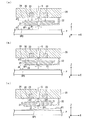
図3は、第1実施形態の表面検出装置の動作を示す説明図である。図3(a)は、基板Pの表面の凹凸を平均化した平面(以下、主面という)が表面検出装置9と対向している状態を示す図、図3(b)は、上記の主面に対して外部に凸である部分の基板Pの表面が表面検出装置9と対向している状態を示す図、図3(c)は、上記の主面に対して傾斜した部分の基板Pの表面が表面検出装置9と対向している状態を示す図である。
FIG. 3 is an explanatory diagram illustrating the operation of the surface detection apparatus according to the first embodiment. FIG. 3A is a view showing a state in which a flat surface (hereinafter referred to as a main surface) in which unevenness on the surface of the substrate P is averaged is opposed to the
図3(a)に示すように、表面検出装置9が基板Pに対向している状態で、上記の流体供給部GSから流体Gが供給される。本例では、吹出口24と流入口27とが不連続(非接触)な状態で、吹出口24から流体Gが吹出される。第1部材20の吹出口24から吹出された流体Gの一部は、第1部材20の下面26と第2部材21の上面30との間の空間SP1を流れる。
As shown in FIG. 3A, the fluid G is supplied from the fluid supply unit GS with the
第1部材20の吹出口24から吹出された流体Gの一部は、第2部材21の流入口27に流入する。流入口27を通って流出口28から流出した流体Gは、基板Pの表面P1と第2部材21の下面31との間の空間SP2を流れる。第2部材21は、空間SP2を流れる流体Gから、基板Pの表面P1から離れる方向の流体力を受ける。本例の第2部材21は、流体Gから受ける流体力によって+Z側に移動(浮上)し、第3部材22と非接触になる。本例では、第2部材21が第3部材22と非接触である状態で、第2部材21のZ方向での位置は、第2部材の下面31と基板Pの表面P1との間の距離d2と関係性がある。本例では、第2部材21が、基板Pの表面P1との距離d2が所定値になる位置でバランスする。距離d2は、流体Gの質量や流量、第2部材21の重量、孔29の形状等のパラメータによって定まる。距離d2が、例えば1μm以上100μm以下、あるいは3μm以上30μm以下になるように、上記のパラメータを設定してもよい。
A part of the fluid G blown from the
検出部23は、第2部材21が第3部材22と非接触である状態で、第2部材21の上面30と検出部23(第1部材20の下面26)との距離d1を検出する。上記のように、距離d2は設定可能な値であり、第2部材21の寸法は既知であるので、検出された距離d1に基づいて表面P1のZ方向の位置を検出することができる。
The
本例では、検出部23の検出結果が記憶装置5に格納される。本例では、複数の検出部23が、第2部材21の上面30上で互いに異なる箇所で第2部材21の位置を検出する。複数の検出部23の検出結果を用いて、例えば補間処理を行うことにより、上面30上で検出箇所と異なる箇所でのZ方向の位置を求めてもよい。例えば、孔29が配置されている箇所での第2部材21のZ方向の位置を求めることもできる。表面検出装置9は、補間処理等の各種演算を実行する演算部を含んでいてもよい。第2部材21のZ方向の位置を求める上での補間処理等の各種演算については、制御装置4が実行してもよい。
In this example, the detection result of the
本例では、基板Pと表面検出装置9との対向方向の交差方向に、基板Pと表面検出装置9との相対位置を変化させながら、基板Pの表面の複数箇所を検出対象箇所として、上記の対向方向における各検出対象箇所の位置を検出する。本例では、上記の対向方向がZ方向であり、上記の交差方向がX方向とY方向の少なくとも一方を含む。本例では、基板Pと表面検出装置9との相対位置が第1相対位置であるときの検出結果と、第1相対位置と異なる第2相対位置であるときの検出結果とを用いて、第2部材21のZ方向の位置を示す情報を補間する。本例では、第1相対位置と第2相対位置との間の任意の相対位置であるときの第2部材21のZ方向の位置を、補間処理により求める。この補間処理の各種演算については、制御装置4が実行してもよい。
In this example, while changing the relative position of the substrate P and the
図3(b)に示すように、基板Pの表面P1が上記の主面よりも凸であると、表面P1が主面である場合と比較して、第2部材21が基板Pから離れる方向(+Z側)に変位する。基板Pの表面P1が主面よりも凸であると、表面P1が主面である場合と比較して、第1部材20の下面26と第2部材21の上面30との距離d1が減少する。本例では、距離d2が上記の所定値になるように、距離d1は表面P1の局所的な高さに応じた値に変化する。すなわち、距離d1の検出結果に基づいて、基板Pの表面P1の凹凸を検出することができる。例えば、基板Pと表面検出装置9のX方向の相対位置を連続的又は断続的に変化させつつ、距離d1を検出することにより、表面P1のX方向での形状を求めることができる。同様にして表面P1のY方向での形状を求めることもできる。
As shown in FIG. 3B, when the surface P1 of the substrate P is more convex than the main surface, the direction in which the
このように、基板Pの表面の凹凸(段差)の二次元的な分布を求めることができ、得られた結果から上記の主面を規定することもできる。例えば、基板Pと表面検出装置9との相対位置をX方向及びY方向に変化させたときの、第2部材21のZ方向の位置の変化量(段差)を検出し、得られた段差分布の平均値などからZ方向の基準となる位置(高さ)を設定することができる。基準となる位置の平面を上記の主面として、基板Pの表面P1の凹凸を求めることもできる。
Thus, the two-dimensional distribution of the irregularities (steps) on the surface of the substrate P can be obtained, and the main surface can be defined from the obtained results. For example, when the relative position between the substrate P and the
図3(c)に示すように、上記の主面に対して傾斜した部分の基板Pが表面検出装置9と対向していると、表面検出装置9が主面に対向している場合と比較して、第2部材21の姿勢が変化する。本例では、第2部材21が基板Pの表面P1に追従するように第2部材21の姿勢が変化する。すると、複数の検出部23により検出される距離d3、d4が互いに異なる値になり得る。本例では、複数の検出部23により検出された距離d3、d4の違いに基づいて、第2部材21の姿勢の変化を検出可能である。第2部材21の姿勢の変化を検出することにより、基板Pの表面P1の傾斜、形状、うねり等を検出することもできる。
As shown in FIG. 3C, when the substrate P in a portion inclined with respect to the main surface is opposed to the
以上のように、第1実施形態にあっては、第2部材21の位置を検出することによって検出対象面を検出することができるので、基板Pの光学特性に依らずに表面P1を検出することが期待できる。したがって、基板Pに対するフォーカス等の露光条件を高精度に設定可能になることが期待できる。よって、基板Pに対する露光不良の発生が抑制され、不良デバイスの発生が抑制されることが期待できる。
As described above, in the first embodiment, since the detection target surface can be detected by detecting the position of the
次に、表面検出装置の変形例について説明する。以下の説明では、上記の実施形態と同様の構成要素に同じ符号を付して、重複する説明を省略することがある。 Next, a modification of the surface detection device will be described. In the following description, the same code | symbol may be attached | subjected to the component similar to said embodiment, and the overlapping description may be abbreviate | omitted.
図4(a)は、変形例1の表面検出装置の概略構成を示す側断面図である。本例の表面検出装置9Bは、第1部材20B、第2部材21B、第3部材22B、及び検出部23を含む。本例の第1部材20Bは、第2部材21Bと対向して配置される下面26Bを有する。本例の下面26Bは、第2部材21Bと対向する部分が第2部材21に対して凹状の曲面である。本例の第2部材21Bは、第1部材20Bと対向する上面30Bを有する。本例の第2部材21Bの上面30Bは、第1部材20Bに対して凸状の曲面である。本例では、第1部材20Bの下面26Bが、第2部材21Bの上面30Bにならう形状に設定されている。本例の第3部材22Bは、第1部材20Bと第2部材21Bとが対向する方向(Z方向)に対する、第1部材20Bの側面に接続されている。
FIG. 4A is a side cross-sectional view illustrating a schematic configuration of the surface detection device of the first modification. The
図4(b)は、変形例2の表面検出装置の概略構成を示す側断面図である。本例の表面検出装置9Cは、第1部材20B、第2部材21C、第3部材22B、及び検出部23を含む。本例の第2部材21Cは、第2部材21Cと対向する上面30Bと、上面30Bとは異なる方向を向く下面31Cとを有する。下面31Cは、検出対象面に対向するように配置される。本例の下面31Cは、検査対象面に向かって凸状の曲面である。
FIG. 4B is a side cross-sectional view illustrating a schematic configuration of the surface detection device of the second modification. The surface detection apparatus 9C of this example includes a
図5は、変形例3の表面検出装置の概略構成を示す図である。図5(a)は、表面検出装置9Dを下方(−Z側)から、第2部材21を透かして見た平面図に相当し、図5(b)は、図5(a)のB−B’線断面図に相当する。
FIG. 5 is a diagram illustrating a schematic configuration of a surface detection device according to the third modification. FIG. 5A corresponds to a plan view of the
本例の表面検出装置9Dは、第1部材20、第2部材21、第3部材22B、及び検出部23Dを含む。本例の第1部材20は、流体Gの吹出口24と、吹出口24に接続された内部流路25とを含む。本例の検出部23Dは、静電容量計を含む。本例の検出部23Dは、吹出口24を環状に囲むように配置されている。本例の検出部23Dは、第1部材20の内部流路25と連通する貫通孔33Dを含む。内部流路25に供給された流体Gは、吹出口24から貫通孔33Dを通って、第2部材21に向けて吹出される。なお、複数の検出部が設けられており、1以上の検出部が静電容量計を含み、他の検出部が干渉計を含んでいてもよい。例えば、検出部23Dの周囲に、干渉計を含む検出部が1以上配置されていてもよい。
The
図6は、変形例4の表面検出装置の概略構成を示す図である。図6(a)は、表面検出装置9Eの外観図、図6(b)は、図6(a)のC−C’線断面図に相当する。
FIG. 6 is a diagram illustrating a schematic configuration of a surface detection device according to a fourth modification. FIG. 6A corresponds to an external view of the
本例の表面検出装置9Eは、基板Pの搬送経路に配置されている。本例の基板Pの搬送方向はY方向である。本例では、基板Pの表面を検出するときに、表面検出装置9Eが搬送経路に対して固定されている。本例の表面検出装置9Eは、第1部材20E、複数の第2部材21、複数の第3部材22、及び複数の検出部23を含む。本例の表面検出装置9Eは、複数の検出セクション34Eを含む。本例の複数の検出セクション34Eは、基板Pの搬送方向(Y方向)に交差する方向に配列されている。本例の複数の検出セクション34Eは、搬送方向に直交する方向(X方向)に配列されている。本例の表面検出装置9Eは、検出セクション34Eが配置される位置のそれぞれにおいて、基板Pの表面を検出可能である。本例の第2部材21は、検出セクション34Eごとに配置されている。本例の第3部材22は、第2部材21ごとに配置されている。本例の第1部材20Eは、第2部材21ごとに設けられた内部流路25を含む。本例の流体供給部GSは、複数の内部流路25に流体Gを供給する。本例では、流体供給部GSからの流路が分岐しており、分岐した流路のそれぞれが第1部材20Eの内部流路25と接続されている。
The
図7は、変形例5の表面検出装置の概略構成を示す側断面図である。本例の表面検出装置9Fは、第1部材20、複数の第2部材21F、及び検出部23を含む。複数の第2部材21Fは、それぞれ、吹出口24からの流体Gの少なくとも一部が流入する流入口27、及び流入口27を通った流体Gが基板Pの表面に向けて流出する流出口28を有する。本例において、複数の第2部材21Fは、いずれも寸法及び形状が同じである。複数の第2部材21Fは、寸法及び形状の少なくとも一方が互いに異なっていても構わない。本例では、第1部材20と基板Pの表面との間に4つの第2部材21Fが配置される。なお、第2部材21Fの数は、2又は3でもよく、5以上でもよい。
FIG. 7 is a side cross-sectional view showing a schematic configuration of a surface detection device of Modification 5. The
本例において、複数の第2部材21Fのそれぞれを、第1部材20から基板Pの表面に向かう方向(−Z方向)に並ぶ順に、第1の第2部材21F、第2の第2部材21F、第3の第2部材21F、第4の第2部材21Fと称することがある。本例において、吹出口24から吹出された流体Gの少なくとも一部は、第1の第2部材21Fの流入口27に流入する。第1の第2部材21Fの流入口27に流入した流体Gは、第1の第2部材21Fの内部を流れた後に、第1の第2部材21Fの流出口28から流出する。第1の第2部材21Fの流出口28から流出した流体Gの少なくとも一部は、第2の第2部材21Fの流入口27に流入し、第2の第2部材21Fの内部及び流出口28を経由して流れる。以下同様にして、吹出口24から吹出された流体Gの少なくとも一部は、複数の第2部材21Fのそれぞれの流入口27と流出口28とを経由して、基板Pの表面に向って流れることが可能である。
In the present example, the first
本例において、検出部23は、流出口28から流出する流体Gの流れ方向における第1の第2部材21Fの位置を検出する。本例において、検出部23の検出結果に基づいて、基板Pの表面を検出することが可能である。なお、検出部23は、第1の第2部材21F以外の第2部材21Fの位置を検出してもよいし、2以上の第2部材21Fの位置を検出してもよい。また、本例において、表面処理装置は、2以上の検出部を含み、検出部が、それぞれ、流出口28から流出する流体Gの流れ方向における、1以上の第2部材21Fの位置を検出してもよい。本例において、表面処理装置は、流出口28から流出する流体Gの流れ方向と交差する方向、例えばZ方向に交差する方向から、第2部材21FのZ方向の位置を検出可能な他の検出部を、検出部23の他に有していてもよく、この検出部によって、検出部23とは異なる検出対象の第2部材21Fの位置を検出しても構わない。
In this example, the
図8(a)は、変形例6の表面検出装置の概略構成を示す側断面図、図8(b)は変形例6における第2部材を示す平面図である。本例の表面検出装置9Gは、第1部材20、第2部材21G、及び検出部23を含む。本例の第2部材21Gは、本体部40、及び複数の翼部41を有する。本例の本体部40は、吹出口24からの流体Gの少なくとも一部が流入する流入口27、及び流入口27を通った流体Gが基板Pの表面に向けて流出する流出口28を有する。
FIG. 8A is a side cross-sectional view showing a schematic configuration of the surface detection device of Modification Example 6, and FIG. 8B is a plan view showing a second member in Modification Example 6. FIG. The
本例の複数の翼部41は、本体部40の周囲に離散的に配置されている。本例の複数の翼部41は、流出口28から流出する流体Gの流れ方向(Z方向)の周りに、等間隔で配置されている。本例の翼部41は、本体部40から本体部40の外側に張り出している。本例の翼部41は、流体を受けて、流出口28から流出する流体Gの流れ方向の周りに第2部材21Gを回転させる回転力を発生可能である。本例の翼部41は、吹出口24から吹出された流体Gを受けて、上記の回転力を発生可能である。
The plurality of
本例の第2部材21は、翼部41に発生した回転力によって、Z方向の周りに回転可能である。本例の表面検出装置は、第2部材21を回転させることにより、例えば第2部材21の姿勢(Z方向に対する傾き)を制御すること等ができる。本例の表面検出装置は、第2部材21を回転させることにより、例えば第2部材21の姿勢を安定させることができる。
The
なお、翼部41の数は、1以上3以下でもよいし、5以上でもよい。複数の翼部41の間隔は、等間隔でもまた不等間隔でも構わない。翼部41は、流入口27と本体部40の縁端との間の本体部40の表面に配置されていてもよいし、流出口28と本体部40の縁端との間の本体部40の表面に配置されていてもよい。翼部41は、流入口27と流出口28との間に配置されていても構わない。また、翼部41は、吹出口24からの流体G以外の流体を受けて、上記の回転力を発生しても構わない。本例において、表面検出装置9Gは、翼部41が上記の回転力を発生させるように、翼部41に流体を供給する装置を含んでもよい。また、本例において、第2部材21Fは、流体から受ける力以外の力によって、流出口28から流出する流体Gの流れ方向の周りに回転可能でもよい。例えば、第2部材21Fは、流体力、静電気力、及び磁力の1以上を受けて、回転可能でもよい。
The number of
図9(a)は、変形例7における第2部材の平面図、図9(b)は図9(a)のD−D’線断面図、図9(c)は図9(a)のE−E’線断面図である。変形例7における第2部材21Hは、第1溝部42及び第2溝部43を含む。本例では、第1溝部42及び第2溝部43は、第2部材21Hにおいて第1部材20に向く上面30に配置されている。本例において、第1溝部42及び第2溝部43は、それぞれ、Z方向に対する放射方向に延びている。本例において、第1溝部42は、第2溝部43と交差して延びている。本例において、第1溝部42及び第2溝部43は、流入口27に通じている。
9A is a plan view of the second member in
なお、第1溝部42及び第2溝部43の一方は、設けられていなくとも構わない。第1溝部42及び第2溝部43の少なくとも一方は、流入口27と交わらなくとも構わない。第1溝部42及び第2溝部43の少なくとも一方は、上記の放射方向に曲線的に延びる部分を含んでもよい。第1溝部42及び第2溝部43の他に、他の溝部が設けられてもよい。他の溝部は、第2部材21Hにおいて上面30とは異なる方向を向く面、例えば基板Pの表面を向く下面に設けられていてもよいし、上面30及び下面の双方に設けられていてもよい。上面30とは異なる方向を向く面に他の溝部が設けられている場合に、第1溝部42と第2溝部43の少なくとも一方は、省略可能である。他の溝部は、流出口28に通じていてもよいし、通じていなくとも構わない。
One of the
本例において、第1溝部42の底部42aの少なくとも一部は、第2部材21Hの上面30と段差を有する。本例において、第1溝部42の底部の少なくとも一部は、第2部材21Hの上面30と段差を有する。本例において、例えば図2に示した第1部材20の吹出口24から吹出された流体Gは、第1溝部42及び第2溝部43の内側を流れる。本例において、流体Gは、第1溝部42の内側を、第1溝部42の延在方向に沿って流れる。本例において、流体Gは、第2溝部43の内側を、第2溝部43の延在方向に沿って流れる。本例の表面検出装置は、例えば、第2部材21Hの周囲の流体Gの流れを制御することができ、例えば第2部材21Hの周囲の流体Gの流れを安定させることができる。
In this example, at least a part of the
なお、第1溝部42、第2溝部43、及び他の溝部の1以上の内側を流体Gが流れなくとも構わない。流体Gは、第1溝部42、第2溝部43、及び他の溝部の1以上について、溝部の延在方向と交差して流れても構わない。本例では、第2部材21Hに溝部が設けられているが、例えば例えば図2に示した第1部材20において、第2部材21に向く面に溝部が設けられていてもよい。
Note that the fluid G may not flow through one or more inner sides of the
図10(a)は、変形例8における第2部材の平面図、図10(b)は図10(a)F−F’線断面図である。変形例8における第2部材21Jは、第1溝部42、第2溝部43、及び第3溝部44を含む。本例では、第3溝部44は、第2部材21Hにおいて第1部材20に向く上面30に配置されている。本例において、第3溝部44は、流出口28から流出する流体Gの流れ方向(Z方向)の周りの周方向に延びている。本例において、第3溝部44の底部44aの少なくとも一部は、第2部材21Jの上面30と段差を有し、かつ第1溝部42の底部42aと段差を有する。本例において、第3溝部44の底部44aの少なくとも一部は、上面30に対して、第1溝部42の底部42aよりも窪んでいる。
FIG. 10A is a plan view of the second member in Modification 8, and FIG. 10B is a cross-sectional view taken along line F-F ′ in FIG. The
なお、本例において、第2部材21Jは、Z方向に対する放射方向に延びる第1溝部42及び第2溝部43と、Z方向周りの周方向に延びる第3溝部44とを有しているが、第1溝部42及び第2溝部43の少なくとも一方は、設けられていなくとも構わない。また、第3溝部44は、上面30とは異なる方向を向く面、例えば基板Pの表面を向く下面に設けられていてもよいし、上面30及び下面の双方に設けられていてもよい。
In this example, the
なお、上記の例で説明した表面検出装置あるいは表面検出方法は、その検出結果を露光以外の処理に利用してもよいし、露光対象の基板以外の物体の表面を検出することに利用してもよい。例えば、製造過程のデバイス(中間体)の検査、あるいは、製造されたデバイスの検査を行う装置として、上記の例で説明した表面検出装置を備える検査装置を利用してもよい。 The surface detection apparatus or the surface detection method described in the above example may use the detection result for processing other than exposure, or may be used for detecting the surface of an object other than the substrate to be exposed. Also good. For example, an inspection apparatus including the surface detection apparatus described in the above example may be used as an apparatus for inspecting a device (intermediate) in a manufacturing process or an inspection of a manufactured device.
なお、液浸露光装置において、例えば国際公開第2004/019128号パンフレットに開示されているように、投影光学系PLの射出面に対して入射側(物体面側)の光路も露光用の液体LQ1で満たされる投影光学系PLを採用することができる。露光用の液体LQ1は、水以外の液体であってもよい。液体LQ1は、露光光ELに対して透過性であり、露光光ELに対して高い屈折率を有し、投影光学系PLあるいは基板Pの表面を形成する感光材(フォトレジスト)などの膜に対して安定なものが好ましい。例えば、液体LQ1として、ハイドロフロロエーテル(HFE)、過フッ化ポリエーテル(PFPE)、フォンブリンオイル等を用いることも可能である。また、液体LQ1、例えば超臨界流体を用いることも可能である。 In the immersion exposure apparatus, as disclosed in, for example, International Publication No. 2004/019128, the light path on the incident side (object surface side) with respect to the exit surface of the projection optical system PL is also the exposure liquid LQ1. The projection optical system PL satisfying the above can be employed. The exposure liquid LQ1 may be a liquid other than water. The liquid LQ1 is transmissive to the exposure light EL, has a high refractive index with respect to the exposure light EL, and is formed on a film such as a photosensitive material (photoresist) that forms the surface of the projection optical system PL or the substrate P. A stable material is preferred. For example, as the liquid LQ1, hydrofluoroether (HFE), perfluorinated polyether (PFPE), fomblin oil, or the like can be used. It is also possible to use a liquid LQ1, for example a supercritical fluid.
露光装置EXとしては、スキャニングステッパの他に、マスクMと基板Pとを静止した状態でマスクMのパターンを一括露光し、基板Pを順次ステップ移動させるステップ・アンド・リピート方式の投影露光装置(ステッパ)にも適用することができる。ステップ・アンド・リピート方式の露光において、第1パターンと基板Pとをほぼ静止した状態で、投影光学系を用いて第1パターンの縮小像を基板P上に転写した後、第2パターンと基板Pとをほぼ静止した状態で、投影光学系を用いて第2パターンの縮小像を第1パターンと部分的に重ねて基板P上に一括露光してもよい(スティッチ方式の一括露光装置)。スティッチ方式の一括露光装置は、基板P上で少なくとも2つのパターンを部分的に重ねて転写し、基板Pを順次移動させるステップ・アンド・スティッチ方式でもよい。例えば米国特許第6611316号明細書に開示されているように、2つのマスクのパターンを、投影光学系を介して基板上で合成し、1回の走査露光によって基板上の1つのショット領域をほぼ同時に二重露光する露光装置などにも本発明を適用することができる。プロキシミティ方式の露光装置、ミラープロジェクション・アライナーなどにも本発明を適用することができる。 As the exposure apparatus EX, in addition to the scanning stepper, the pattern of the mask M is collectively exposed while the mask M and the substrate P are stationary, and the substrate P is sequentially moved step by step. It can also be applied to steppers). In step-and-repeat exposure, after a reduced image of the first pattern is transferred onto the substrate P using the projection optical system with the first pattern and the substrate P being substantially stationary, the second pattern and the substrate are transferred. In a state where P is substantially stationary, a reduced image of the second pattern may be overlapped with the first pattern using the projection optical system and may be collectively exposed on the substrate P (stitch type batch exposure apparatus). The stitch type batch exposure apparatus may be a step-and-stitch type in which at least two patterns are partially transferred on the substrate P and transferred, and the substrate P is sequentially moved. For example, as disclosed in US Pat. No. 6,611,316, a pattern of two masks is synthesized on a substrate via a projection optical system, and one shot area on the substrate is approximately formed by one scanning exposure. The present invention can also be applied to an exposure apparatus that performs double exposure at the same time. The present invention can also be applied to proximity type exposure apparatuses, mirror projection aligners, and the like.
露光装置EXは、例えば米国特許第6897963号明細書、及び欧州特許出願公開第1713113号明細書等に開示されているような基板ステージと計測ステージとを備えた露光装置でもよい。この計測ステージに搭載される計測部材は、例えば米国特許出願公開第2002/0041377号明細書等に開示されているような空間像計測システムの一部を構成する部材でもよいし、米国特許第4465368号明細書等に開示されているような照度むら計測システムの一部を構成する部材でもよいし、米国特許第5493403号明細書等に開示されているような基準部材でもよいし、米国特許出願公開第2002/0061469号明細書等に開示されているような照射量計測システムの一部を構成する部材でもよいし、欧州特許第1079223号明細書等に開示されているような波面収差計測システムの一部を構成する部材でもよい。上記の例で説明した表面検出装置は、計測ステージに配置されていてもよい。計測ステージに、例えば光学的に基板の表面を検出する光学検出装置が配置されている場合に、光学検出装置の検出結果を、上記の例で説明した表面検出装置の検出結果と比較してもよく、検出の成否の判定や互いの検出結果の相互補間等に利用してもよい。 The exposure apparatus EX may be an exposure apparatus including a substrate stage and a measurement stage as disclosed in, for example, US Pat. No. 6,897,963 and European Patent Application Publication No. 1713113. The measurement member mounted on the measurement stage may be a member constituting a part of an aerial image measurement system as disclosed in, for example, US Patent Application Publication No. 2002/0041377, or US Pat. No. 4,465,368. It may be a member constituting a part of an uneven illuminance measuring system as disclosed in the specification of the US Patent No. 5,493,403, a reference member as disclosed in US Pat. No. 5,493,403, etc. It may be a member constituting a part of a dose measuring system as disclosed in the specification of Japanese Patent Publication No. 2002/0061469 or the like, or a wavefront aberration measuring system as disclosed in the specification of European Patent No. 1079223 The member which comprises a part of may be sufficient. The surface detection apparatus described in the above example may be disposed on the measurement stage. For example, when an optical detection device that optically detects the surface of the substrate is disposed on the measurement stage, the detection result of the optical detection device may be compared with the detection result of the surface detection device described in the above example. Of course, it may be used for determination of success or failure of detection, mutual interpolation of detection results of each other, and the like.
露光装置EXは、米国特許第6341007号明細書、米国特許第6208407号明細書、米国特許第6262796号明細書等に開示されているような、計測ステージを備えておらず、複数の基板ステージを備えたツインステージ型の露光装置でもよい。その場合、複数の基板ステージのうち、任意の基板ステージに上記の例で説明した表面検出装置を配置してもよい。 The exposure apparatus EX does not include a measurement stage as disclosed in US Pat. No. 6,341,007, US Pat. No. 6,208,407, US Pat. No. 6,262,796, etc., and includes a plurality of substrate stages. A twin stage type exposure apparatus provided may be used. In that case, you may arrange | position the surface detection apparatus demonstrated in said example to arbitrary board | substrate stages among several board | substrate stages.
基板Pの基材は、半導体デバイス製造用の半導体ウエハのみならず、ディスプレイデバイス用のガラス基板、薄膜磁気ヘッド用のセラミックウエハ、あるいは露光装置で用いられるマスクまたはレチクルの原版(合成石英、シリコンウエハ)等であってもよい。露光装置EXの種類としては、基板Pに半導体素子パターンを露光する半導体素子製造用の露光装置や、液晶表示素子製造用又はディスプレイ製造用の露光装置、薄膜磁気ヘッド、撮像素子(CCD)、マイクロマシン、MEMS、DNAチップ、あるいはレチクル又はマスクなどを製造するための露光装置などにも広く適用できる。 The base material of the substrate P is not only a semiconductor wafer for manufacturing semiconductor devices, but also a glass substrate for display devices, a ceramic wafer for thin film magnetic heads, or a mask or reticle used in an exposure apparatus (synthetic quartz, silicon wafer) Or the like. As types of the exposure apparatus EX, an exposure apparatus for manufacturing a semiconductor element that exposes a semiconductor element pattern onto a substrate P, an exposure apparatus for manufacturing a liquid crystal display element or a display, a thin film magnetic head, an image sensor (CCD), a micromachine , MEMS, DNA chips, or exposure apparatuses for manufacturing reticles or masks can be widely applied.
上記の例では、干渉計を用いて各ステージの位置情報を計測するものとしたが、これに限らず、例えば各ステージに設けられるスケール(回折格子)を検出するエンコーダシステムを用いてもよい。 In the above example, the position information of each stage is measured using an interferometer. However, the present invention is not limited to this, and for example, an encoder system that detects a scale (diffraction grating) provided in each stage may be used.
上記の例では、光透過性の基板上に所定の遮光パターン(又は位相パターン・減光パターン)を形成した光透過型マスクを用いたが、このマスクに代えて、例えば米国特許第6778257号明細書に開示されているように、露光すべきパターンの電子データに基づいて透過パターン又は反射パターン、あるいは発光パターンを形成する可変成形マスク(電子マスク、アクティブマスク、あるいはイメージジェネレータとも呼ばれる)を用いてもよい。また、非発光型画像表示素子を備える可変成形マスクに代えて、自発光型画像表示素子を含むパターン形成装置を備えるようにしても良い。 In the above example, a light transmissive mask in which a predetermined light shielding pattern (or phase pattern / dimming pattern) is formed on a light transmissive substrate is used. Instead of this mask, for example, US Pat. No. 6,778,257 is disclosed. As disclosed in this document, using a variable shaping mask (also called an electronic mask, an active mask, or an image generator) that forms a transmission pattern, a reflection pattern, or a light emission pattern based on electronic data of a pattern to be exposed. Also good. Further, a pattern forming apparatus including a self-luminous image display element may be provided instead of the variable molding mask including the non-luminous image display element.
上記の例では、投影光学系PLを備えた露光装置を例に挙げて説明したが、投影光学系PLを用いない露光装置及び露光方法に本発明を適用することができる。例えば、レンズ等の光学部材と基板との間に液浸空間を形成し、その光学部材を介して、基板に露光光を照射することができる。また、例えば国際公開第2001/035168号パンフレットに開示されているように、干渉縞を基板P上に形成することによって、基板P上にライン・アンド・スペースパターンを露光する露光装置(リソグラフィシステム)にも本発明を適用することができる。 In the above example, the exposure apparatus provided with the projection optical system PL has been described as an example. However, the present invention can be applied to an exposure apparatus and an exposure method that do not use the projection optical system PL. For example, an immersion space can be formed between an optical member such as a lens and the substrate, and the substrate can be irradiated with exposure light through the optical member. Further, as disclosed in, for example, International Publication No. 2001/035168, an exposure apparatus (lithography system) that exposes a line and space pattern on the substrate P by forming interference fringes on the substrate P. The present invention can also be applied to.
上記の例の露光装置EXは、本願請求の範囲に挙げられた各構成要素を含む各種サブシステムを、所定の機械的精度、電気的精度、光学的精度を保つように、組み立てることで製造される。これら各種精度を確保するために、この組み立ての前後には、各種光学系については光学的精度を達成するための調整、各種機械系については機械的精度を達成するための調整、各種電気系については電気的精度を達成するための調整が行われる。各種サブシステムから露光装置への組み立て工程は、各種サブシステム相互の、機械的接続、電気回路の配線接続、気圧回路の配管接続等が含まれる。この各種サブシステムから露光装置への組み立て工程の前に、各サブシステム個々の組み立て工程があることはいうまでもない。各種サブシステムの露光装置への組み立て工程が終了したら、総合調整が行われ、露光装置全体としての各種精度が確保される。なお、露光装置の製造は温度およびクリーン度等が管理されたクリーンルームで行うことが望ましい。 The exposure apparatus EX in the above example is manufactured by assembling various subsystems including the constituent elements recited in the claims of the present application so as to maintain predetermined mechanical accuracy, electrical accuracy, and optical accuracy. The In order to ensure these various accuracies, before and after assembly, various optical systems are adjusted to achieve optical accuracy, various mechanical systems are adjusted to achieve mechanical accuracy, and various electrical systems are Adjustments are made to achieve electrical accuracy. The assembly process from the various subsystems to the exposure apparatus includes mechanical connection, electrical circuit wiring connection, pneumatic circuit piping connection and the like between the various subsystems. Needless to say, there is an assembly process for each subsystem before the assembly process from the various subsystems to the exposure apparatus. When the assembly process of the various subsystems to the exposure apparatus is completed, comprehensive adjustment is performed to ensure various accuracies as the entire exposure apparatus. The exposure apparatus is preferably manufactured in a clean room where the temperature, cleanliness, etc. are controlled.
上記の各例の要件は、適宜組み合わせることができる。また、一部の構成要素を用いない場合もある。また、法令で許容される限りにおいて、上記の例で引用した露光装置などに関する全ての公開公報及び米国特許の開示を援用して本文の記載の一部とする。 The requirements of the above examples can be combined as appropriate. Some components may not be used. In addition, as long as it is permitted by law, the disclosure of all published publications and US patents related to the exposure apparatus and the like cited in the above examples are incorporated herein by reference.
<第2実施形態>
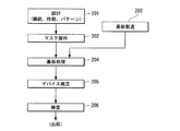
図11は、第2実施形態のデバイス製造方法の一例を示すフローチャートである。半導体デバイス等のマイクロデバイスは、マイクロデバイスの機能・性能設計を行うステップ201、この設計ステップに基づいたマスク(レチクル)を製作するステップ202、デバイスの基材である基板を製造するステップ203、基板に成膜処理や露光処理、現像処理、エッチング処理等の各種基板処理を行う基板処理ステップ204、デバイス組立ステップ205、検査ステップ206等を経て製造される。
Second Embodiment
FIG. 11 is a flowchart illustrating an example of a device manufacturing method according to the second embodiment. For a microdevice such as a semiconductor device, a
基板処理ステップ204は、上記の実施形態に従って露光対象の基板の表面を検出すること(以下、第1検出処理という)、露光光で基板を露光すること、及び露光された基板を現像することを含む。本例の基板処理ステップ204は、露光対象の基板に検出光を照射して基板の表面を光学的に検出すること(以下、第2検出処理という)と、第1検出処理の検出結果と第2検出処理の検出結果とを比較することとを含む。第2検出処理は、基板の露光前に行ってもよいし、基板の一部の露光と並行して行ってもよい。例えば、基板に複数の膜(層)が積層されている場合に、第2検出処理において基板に照射された検出光の一部が、各層で屈折あるいは反射することがありえる。すると、実際の基板の表面と異なる位置、例えば各層の界面の位置が、基板の表面の位置として検出されることがありえる。また、第2検出処理の結果において、基板の表面の位置として複数の位置が検出されることもありえる。本例では、第1検出処理の検出結果と第2検出処理の検出結果とを比較して、基板の表面の位置を決定する。なお、表面を検出する基板上の検出箇所の間隔を、第2検出処理において第1検出処理よりも狭く設定してもよい。例えば、第1検出処理において第1解像度で基板の表面を検出し、第2検出処理において第1解像度よりも高い第2解像度で基板の表面を検出してもよい。また、第1解像度で検出した検出結果と、第2解像度で検出した検出結果とを相互補間してもよい。本例の基板処理ステップ204では、基板の表面を検出した検出結果に基づいて基板の表面に光学系の焦点をあわせた状態で、この光学系を介して基板にパターンの像を投影して露光する。デバイス組立ステップ205は、ダイシング工程、ボンディング工程、パッケージ工程などの加工プロセスを含む。検査ステップ206で、上記の実施形態で説明した表面検出装置あるいは表面検出方法を用いて、製造されたデバイスを検査してもよい。また、デバイス製造過程中の適宜選択されるタイミングで、上記の実施形態で説明した表面検出装置あるいは表面検出方法を用いて、製造過程のデバイスを検査してもよい。
In the
EX・・・露光装置、9、9B、9C、9D、9E・・・表面検出装置、
20、20B、20E・・・第1部材、21、21B、21C・・・第2部材、
22、22B・・・第3部材、23、23D・・・検出部、24・・・吹出口、
27・・・流入口、28・・・流出口、G・・・流体、P・・・基板、
GS・・・流体供給部(供給部)、SYS・・・デバイス製造システム
EX ... exposure device, 9, 9B, 9C, 9D, 9E ... surface detection device,
20, 20B, 20E ... 1st member, 21, 21B, 21C ... 2nd member,
22, 22B ... 3rd member, 23, 23D ... detection part, 24 ... blower outlet,
27 ... Inlet, 28 ... Outlet, G ... Fluid, P ... Substrate,
GS ... Fluid supply part (supply part), SYS ... Device manufacturing system
Claims (34)
前記第1部材と検出対象面との間に配置され、前記吹出口からの流体の少なくとも一部が流入する流入口、及び前記流入口を通った流体が前記検出対象面に向けて流出する流出口を有する第2部材と、
前記流出口から流出する流体の流れ方向における前記第2部材の位置を検出する検出部と、を備える表面検出装置。 A first member having a fluid outlet;
An inflow port that is arranged between the first member and the detection target surface and into which at least a part of the fluid from the blowout port flows, and a flow through which the fluid that has passed through the inflow port flows out toward the detection target surface A second member having an outlet;
A surface detection device comprising: a detection unit that detects a position of the second member in a flow direction of the fluid flowing out from the outlet.
前記吹出口からの流体が前記貫通孔を通過して前記流入口に流入する、請求項1〜25のいずれか一項に記載の表面検出装置。 The detector has a through hole;
The surface detection device according to any one of claims 1 to 25, wherein fluid from the blowout port passes through the through hole and flows into the inflow port.
露光された前記基板を現像することと、を含むデバイス製造方法。 Exposing the substrate using the exposure apparatus of claim 28;
Developing the exposed substrate. A device manufacturing method.
前記流入口に流体を供給することと、
前記流出口から流出した流体から前記部材が受ける力によって、前記検出対象面から前記部材を離すことと、
前記流入口に流体が供給されている状態で、前記流出口から流出する流体の流れ方向における前記部材の位置を検出することと、を含む表面検出方法。 Disposing a member having a fluid inflow port and an outflow port through which the fluid flows through the inflow port, with the outflow port facing the detection target surface;
Supplying fluid to the inlet;
Separating the member from the detection target surface by the force received by the member from the fluid flowing out from the outlet;
Detecting a position of the member in a flow direction of the fluid flowing out from the outlet while the fluid is supplied to the inlet.
前記基板の表面に光を照射して前記基板の表面を検出することと、
前記表面検出方法による検出結果と前記光による検出結果とを比較することと、
前記比較の結果に基づいて前記基板を露光することと、を含む露光方法。 Detecting the surface of the substrate using the surface detection method according to any one of claims 30 to 32;
Irradiating the surface of the substrate with light to detect the surface of the substrate;
Comparing the detection result by the surface detection method with the detection result by the light;
Exposing the substrate based on the result of the comparison.
露光された前記基板を現像することと、を含むデバイス製造方法。 Exposing the substrate using the exposure method of claim 33;
Developing the exposed substrate. A device manufacturing method.
Priority Applications (1)
| Application Number | Priority Date | Filing Date | Title |
|---|---|---|---|
| JP2010208375A JP2012064803A (en) | 2010-09-16 | 2010-09-16 | Surface detecting device, exposure device, surface detecting method, exposure method, and device manufacturing method |
Applications Claiming Priority (1)
| Application Number | Priority Date | Filing Date | Title |
|---|---|---|---|
| JP2010208375A JP2012064803A (en) | 2010-09-16 | 2010-09-16 | Surface detecting device, exposure device, surface detecting method, exposure method, and device manufacturing method |
Publications (2)
| Publication Number | Publication Date |
|---|---|
| JP2012064803A true JP2012064803A (en) | 2012-03-29 |
| JP2012064803A5 JP2012064803A5 (en) | 2013-10-31 |
Family
ID=46060193
Family Applications (1)
| Application Number | Title | Priority Date | Filing Date |
|---|---|---|---|
| JP2010208375A Pending JP2012064803A (en) | 2010-09-16 | 2010-09-16 | Surface detecting device, exposure device, surface detecting method, exposure method, and device manufacturing method |
Country Status (1)
| Country | Link |
|---|---|
| JP (1) | JP2012064803A (en) |
Citations (4)
| Publication number | Priority date | Publication date | Assignee | Title |
|---|---|---|---|---|
| JPH05280962A (en) * | 1991-07-12 | 1993-10-29 | Fukae Kosakusho:Kk | Plate material thickness measuring apparatus |
| JPH09280846A (en) * | 1996-04-17 | 1997-10-31 | Hiroshi Akashi | Displacement sensor |
| JP2004053299A (en) * | 2002-07-17 | 2004-02-19 | Tokyo Seimitsu Co Ltd | Machine for measuring thickness in plate-like material work |
| JP2004198430A (en) * | 2002-12-19 | 2004-07-15 | Asml Holding Nv | Liquid flow proximity sensor for use in immersion lithography |
-
2010
- 2010-09-16 JP JP2010208375A patent/JP2012064803A/en active Pending
Patent Citations (4)
| Publication number | Priority date | Publication date | Assignee | Title |
|---|---|---|---|---|
| JPH05280962A (en) * | 1991-07-12 | 1993-10-29 | Fukae Kosakusho:Kk | Plate material thickness measuring apparatus |
| JPH09280846A (en) * | 1996-04-17 | 1997-10-31 | Hiroshi Akashi | Displacement sensor |
| JP2004053299A (en) * | 2002-07-17 | 2004-02-19 | Tokyo Seimitsu Co Ltd | Machine for measuring thickness in plate-like material work |
| JP2004198430A (en) * | 2002-12-19 | 2004-07-15 | Asml Holding Nv | Liquid flow proximity sensor for use in immersion lithography |
Similar Documents
| Publication | Publication Date | Title |
|---|---|---|
| US10739683B2 (en) | Liquid immersion member, exposure apparatus, exposing method, method for manufacturing device, program, and recording medium | |
| KR101303712B1 (en) | Method of updating calibration data and a device manufacturing method | |
| JP5999093B2 (en) | Immersion member, immersion exposure apparatus, device manufacturing method, and immersion exposure method | |
| JP5239337B2 (en) | Exposure method, exposure apparatus, and device manufacturing method | |
| JP2009182359A (en) | Lithographic apparatus | |
| KR20150003276A (en) | Liquid immersion member and exposure apparatus | |
| JP4946109B2 (en) | Exposure method, exposure apparatus, and device manufacturing method | |
| KR101173966B1 (en) | An Immersion Lithographic Apparatus and a Device Manufacturing Method | |
| NL2005974A (en) | Lithographic apparatus and a device manufacturing method. | |
| KR20130103322A (en) | Liquid immersion member and immersion exposure apparatus | |
| JP2011165798A (en) | Aligner, method used by the aligner, method of manufacturing device, program, and recording medium | |
| JP2010040702A (en) | Stage device, exposure system and device manufacturing method | |
| JP5519611B2 (en) | Method for optimizing lithographic process, lithographic apparatus, computer program, and simulation apparatus | |
| JP2012064803A (en) | Surface detecting device, exposure device, surface detecting method, exposure method, and device manufacturing method | |
| JP2012138511A (en) | Control method of exposure device, exposure device, device manufacturing method, program, and recording medium | |
| US20130135594A1 (en) | Liquid immersion member, immersion exposure apparatus, exposure method, device manufacturing method, program, and recording medium | |
| JP2013102029A (en) | Exposure device, exposure method, manufacturing method of device, program, and recording medium | |
| JP2011124415A (en) | Exposure apparatus, exposure method, and method of manufacturing device | |
| JP2006156508A (en) | Method of deciding target value, moving method, exposing method, exposing device, and lithography system | |
| JP2010016256A (en) | Foreign substance detection method, exposure method, and device manufacturing method | |
| JP2013105781A (en) | Substrate holding device, exposure device, and device manufacturing method | |
| JP2013127559A (en) | Mask substrate, photomask, exposure method, device manufacturing method, manufacturing method of mask substrate, manufacturing method of photomask, and manufacturing system | |
| JP2019070861A (en) | Exposure device, exposure method, and device manufacturing method | |
| JP2012138577A (en) | Liquid immersion member, liquid immersion exposure apparatus, exposure method, method for manufacturing device, program, and recording media | |
| JP2012019039A (en) | Exposure method, exposure device, program, recording medium and device manufacturing method |
Legal Events
| Date | Code | Title | Description |
|---|---|---|---|
| A521 | Written amendment |
Free format text: JAPANESE INTERMEDIATE CODE: A523 Effective date: 20130917 |
|
| A621 | Written request for application examination |
Free format text: JAPANESE INTERMEDIATE CODE: A621 Effective date: 20130917 |
|
| A977 | Report on retrieval |
Free format text: JAPANESE INTERMEDIATE CODE: A971007 Effective date: 20140131 |
|
| A131 | Notification of reasons for refusal |
Free format text: JAPANESE INTERMEDIATE CODE: A131 Effective date: 20140204 |
|
| A02 | Decision of refusal |
Free format text: JAPANESE INTERMEDIATE CODE: A02 Effective date: 20140603 |