JP2012024917A - Microstructure with wall of determined optical property and method for making microstructure - Google Patents
Microstructure with wall of determined optical property and method for making microstructure Download PDFInfo
- Publication number
- JP2012024917A JP2012024917A JP2011158777A JP2011158777A JP2012024917A JP 2012024917 A JP2012024917 A JP 2012024917A JP 2011158777 A JP2011158777 A JP 2011158777A JP 2011158777 A JP2011158777 A JP 2011158777A JP 2012024917 A JP2012024917 A JP 2012024917A
- Authority
- JP
- Japan
- Prior art keywords
- layer
- wall
- cavity
- sacrificial
- forming
- Prior art date
- Legal status (The legal status is an assumption and is not a legal conclusion. Google has not performed a legal analysis and makes no representation as to the accuracy of the status listed.)
- Pending
Links
- 238000000034 method Methods 0.000 title claims abstract description 49
- 230000003287 optical effect Effects 0.000 title claims description 39
- 239000000463 material Substances 0.000 claims abstract description 65
- 239000000758 substrate Substances 0.000 claims abstract description 26
- 238000005530 etching Methods 0.000 claims abstract description 19
- VYZAMTAEIAYCRO-UHFFFAOYSA-N Chromium Chemical compound [Cr] VYZAMTAEIAYCRO-UHFFFAOYSA-N 0.000 claims description 10
- 239000012530 fluid Substances 0.000 claims description 8
- 238000010521 absorption reaction Methods 0.000 claims description 7
- 229910003481 amorphous carbon Inorganic materials 0.000 claims description 7
- ZOKXTWBITQBERF-UHFFFAOYSA-N Molybdenum Chemical compound [Mo] ZOKXTWBITQBERF-UHFFFAOYSA-N 0.000 claims description 6
- VYPSYNLAJGMNEJ-UHFFFAOYSA-N Silicium dioxide Chemical compound O=[Si]=O VYPSYNLAJGMNEJ-UHFFFAOYSA-N 0.000 claims description 6
- 229910052750 molybdenum Inorganic materials 0.000 claims description 6
- 239000011733 molybdenum Substances 0.000 claims description 6
- 239000011148 porous material Substances 0.000 claims description 5
- 229910004298 SiO 2 Inorganic materials 0.000 claims description 4
- 238000000151 deposition Methods 0.000 claims description 4
- 229910052581 Si3N4 Inorganic materials 0.000 claims description 3
- 229910052804 chromium Inorganic materials 0.000 claims description 3
- 239000011651 chromium Substances 0.000 claims description 3
- HQVNEWCFYHHQES-UHFFFAOYSA-N silicon nitride Chemical compound N12[Si]34N5[Si]62N3[Si]51N64 HQVNEWCFYHHQES-UHFFFAOYSA-N 0.000 claims description 3
- 229910052814 silicon oxide Inorganic materials 0.000 claims description 3
- AMGQUBHHOARCQH-UHFFFAOYSA-N indium;oxotin Chemical compound [In].[Sn]=O AMGQUBHHOARCQH-UHFFFAOYSA-N 0.000 claims description 2
- 230000002745 absorbent Effects 0.000 abstract description 7
- 239000002250 absorbent Substances 0.000 abstract description 7
- 239000010410 layer Substances 0.000 description 92
- 239000007788 liquid Substances 0.000 description 10
- 238000004519 manufacturing process Methods 0.000 description 10
- 239000011347 resin Substances 0.000 description 9
- 229920005989 resin Polymers 0.000 description 9
- 238000001039 wet etching Methods 0.000 description 8
- 238000010586 diagram Methods 0.000 description 7
- 238000000206 photolithography Methods 0.000 description 5
- KRHYYFGTRYWZRS-UHFFFAOYSA-N Fluorane Chemical compound F KRHYYFGTRYWZRS-UHFFFAOYSA-N 0.000 description 4
- 239000006096 absorbing agent Substances 0.000 description 4
- 238000007789 sealing Methods 0.000 description 4
- 238000005229 chemical vapour deposition Methods 0.000 description 3
- 230000000694 effects Effects 0.000 description 3
- 239000011521 glass Substances 0.000 description 3
- 239000004973 liquid crystal related substance Substances 0.000 description 3
- 238000005240 physical vapour deposition Methods 0.000 description 3
- 238000000623 plasma-assisted chemical vapour deposition Methods 0.000 description 3
- 229920000139 polyethylene terephthalate Polymers 0.000 description 3
- 239000005020 polyethylene terephthalate Substances 0.000 description 3
- 239000002253 acid Substances 0.000 description 2
- 230000032683 aging Effects 0.000 description 2
- 230000007547 defect Effects 0.000 description 2
- 230000008021 deposition Effects 0.000 description 2
- 229910003460 diamond Inorganic materials 0.000 description 2
- 239000010432 diamond Substances 0.000 description 2
- 238000005566 electron beam evaporation Methods 0.000 description 2
- QPJSUIGXIBEQAC-UHFFFAOYSA-N n-(2,4-dichloro-5-propan-2-yloxyphenyl)acetamide Chemical compound CC(C)OC1=CC(NC(C)=O)=C(Cl)C=C1Cl QPJSUIGXIBEQAC-UHFFFAOYSA-N 0.000 description 2
- 239000000049 pigment Substances 0.000 description 2
- 238000001020 plasma etching Methods 0.000 description 2
- 230000001681 protective effect Effects 0.000 description 2
- 235000012239 silicon dioxide Nutrition 0.000 description 2
- 230000003595 spectral effect Effects 0.000 description 2
- DDFHBQSCUXNBSA-UHFFFAOYSA-N 5-(5-carboxythiophen-2-yl)thiophene-2-carboxylic acid Chemical compound S1C(C(=O)O)=CC=C1C1=CC=C(C(O)=O)S1 DDFHBQSCUXNBSA-UHFFFAOYSA-N 0.000 description 1
- 229910017855 NH 4 F Inorganic materials 0.000 description 1
- ATJFFYVFTNAWJD-UHFFFAOYSA-N Tin Chemical compound [Sn] ATJFFYVFTNAWJD-UHFFFAOYSA-N 0.000 description 1
- 239000011358 absorbing material Substances 0.000 description 1
- 230000003373 anti-fouling effect Effects 0.000 description 1
- 238000000231 atomic layer deposition Methods 0.000 description 1
- 230000015572 biosynthetic process Effects 0.000 description 1
- 238000005520 cutting process Methods 0.000 description 1
- 238000001514 detection method Methods 0.000 description 1
- 230000006866 deterioration Effects 0.000 description 1
- 238000009792 diffusion process Methods 0.000 description 1
- 238000007598 dipping method Methods 0.000 description 1
- 238000001704 evaporation Methods 0.000 description 1
- 230000008020 evaporation Effects 0.000 description 1
- 239000012467 final product Substances 0.000 description 1
- 238000010304 firing Methods 0.000 description 1
- 238000003384 imaging method Methods 0.000 description 1
- 229910003437 indium oxide Inorganic materials 0.000 description 1
- PJXISJQVUVHSOJ-UHFFFAOYSA-N indium(iii) oxide Chemical compound [O-2].[O-2].[O-2].[In+3].[In+3] PJXISJQVUVHSOJ-UHFFFAOYSA-N 0.000 description 1
- 238000010030 laminating Methods 0.000 description 1
- 239000002346 layers by function Substances 0.000 description 1
- 239000011344 liquid material Substances 0.000 description 1
- 239000002923 metal particle Substances 0.000 description 1
- 238000004377 microelectronic Methods 0.000 description 1
- 239000005304 optical glass Substances 0.000 description 1
- 239000002245 particle Substances 0.000 description 1
- 239000002985 plastic film Substances 0.000 description 1
- 229920006255 plastic film Polymers 0.000 description 1
- -1 polyethylene terephthalate Polymers 0.000 description 1
- 239000002861 polymer material Substances 0.000 description 1
- 239000000047 product Substances 0.000 description 1
- 239000010453 quartz Substances 0.000 description 1
- 238000007650 screen-printing Methods 0.000 description 1
- 229910052710 silicon Inorganic materials 0.000 description 1
- 239000010703 silicon Substances 0.000 description 1
- 239000000377 silicon dioxide Substances 0.000 description 1
- 239000004094 surface-active agent Substances 0.000 description 1
- 239000012780 transparent material Substances 0.000 description 1
- 238000002604 ultrasonography Methods 0.000 description 1
- XLYOFNOQVPJJNP-UHFFFAOYSA-N water Substances O XLYOFNOQVPJJNP-UHFFFAOYSA-N 0.000 description 1
Images


Classifications
-
- G—PHYSICS
- G02—OPTICS
- G02B—OPTICAL ELEMENTS, SYSTEMS OR APPARATUS
- G02B5/00—Optical elements other than lenses
- G02B5/005—Diaphragms
-
- G—PHYSICS
- G02—OPTICS
- G02B—OPTICAL ELEMENTS, SYSTEMS OR APPARATUS
- G02B1/00—Optical elements characterised by the material of which they are made; Optical coatings for optical elements
- G02B1/10—Optical coatings produced by application to, or surface treatment of, optical elements
-
- G—PHYSICS
- G02—OPTICS
- G02B—OPTICAL ELEMENTS, SYSTEMS OR APPARATUS
- G02B1/00—Optical elements characterised by the material of which they are made; Optical coatings for optical elements
- G02B1/10—Optical coatings produced by application to, or surface treatment of, optical elements
- G02B1/14—Protective coatings, e.g. hard coatings
-
- G—PHYSICS
- G02—OPTICS
- G02F—OPTICAL DEVICES OR ARRANGEMENTS FOR THE CONTROL OF LIGHT BY MODIFICATION OF THE OPTICAL PROPERTIES OF THE MEDIA OF THE ELEMENTS INVOLVED THEREIN; NON-LINEAR OPTICS; FREQUENCY-CHANGING OF LIGHT; OPTICAL LOGIC ELEMENTS; OPTICAL ANALOGUE/DIGITAL CONVERTERS
- G02F1/00—Devices or arrangements for the control of the intensity, colour, phase, polarisation or direction of light arriving from an independent light source, e.g. switching, gating or modulating; Non-linear optics
- G02F1/01—Devices or arrangements for the control of the intensity, colour, phase, polarisation or direction of light arriving from an independent light source, e.g. switching, gating or modulating; Non-linear optics for the control of the intensity, phase, polarisation or colour
- G02F1/13—Devices or arrangements for the control of the intensity, colour, phase, polarisation or direction of light arriving from an independent light source, e.g. switching, gating or modulating; Non-linear optics for the control of the intensity, phase, polarisation or colour based on liquid crystals, e.g. single liquid crystal display cells
- G02F1/133—Constructional arrangements; Operation of liquid crystal cells; Circuit arrangements
- G02F1/1333—Constructional arrangements; Manufacturing methods
- G02F1/133377—Cells with plural compartments or having plurality of liquid crystal microcells partitioned by walls, e.g. one microcell per pixel
-
- G—PHYSICS
- G02—OPTICS
- G02F—OPTICAL DEVICES OR ARRANGEMENTS FOR THE CONTROL OF LIGHT BY MODIFICATION OF THE OPTICAL PROPERTIES OF THE MEDIA OF THE ELEMENTS INVOLVED THEREIN; NON-LINEAR OPTICS; FREQUENCY-CHANGING OF LIGHT; OPTICAL LOGIC ELEMENTS; OPTICAL ANALOGUE/DIGITAL CONVERTERS
- G02F1/00—Devices or arrangements for the control of the intensity, colour, phase, polarisation or direction of light arriving from an independent light source, e.g. switching, gating or modulating; Non-linear optics
- G02F1/01—Devices or arrangements for the control of the intensity, colour, phase, polarisation or direction of light arriving from an independent light source, e.g. switching, gating or modulating; Non-linear optics for the control of the intensity, phase, polarisation or colour
- G02F1/13—Devices or arrangements for the control of the intensity, colour, phase, polarisation or direction of light arriving from an independent light source, e.g. switching, gating or modulating; Non-linear optics for the control of the intensity, phase, polarisation or colour based on liquid crystals, e.g. single liquid crystal display cells
- G02F1/133—Constructional arrangements; Operation of liquid crystal cells; Circuit arrangements
- G02F1/1333—Constructional arrangements; Manufacturing methods
- G02F1/1335—Structural association of cells with optical devices, e.g. polarisers or reflectors
- G02F1/133509—Filters, e.g. light shielding masks
- G02F1/133512—Light shielding layers, e.g. black matrix
Landscapes
- Physics & Mathematics (AREA)
- General Physics & Mathematics (AREA)
- Optics & Photonics (AREA)
- Nonlinear Science (AREA)
- Mathematical Physics (AREA)
- Chemical & Material Sciences (AREA)
- Crystallography & Structural Chemistry (AREA)
- Micromachines (AREA)
Abstract
【課題】マイクロ光学素子のキャビティを形成する方法を提供する。
【解決手段】a)支持基板(10)の平面上に犠牲材料層(12)を形成する段階と、b)キャビティ(4)の底部が前記犠牲材料層によって形成された、前記キャビティの壁(6)を形成する段階と、c)吸収層(30)を、前記壁の頂上(60)、前記壁の側面(61,62)及び前記キャビティの前記底部(4’)に等角的に堆積する段階と、d)前記犠牲層(12)をエッチングし、この層の前記材料及び前記キャビティ(4)の前記底部に存在する前記吸収材料の層(30)の前記材料を除去する段階と、を含むマイクロ光学素子のキャビティ(4)を形成する方法を開示する。
【選択図】図2FA method for forming a cavity of a micro-optical element is provided.
A) forming a sacrificial material layer (12) on a plane of a support substrate (10); and b) a cavity wall (4) in which the bottom of the cavity (4) is formed by the sacrificial material layer. 6) forming c) and absorbing layer (30) is conformally deposited on the top (60) of the wall, side surfaces (61, 62) of the wall and the bottom (4 ') of the cavity. D) etching the sacrificial layer (12) to remove the material of this layer and the material of the layer of absorbent material (30) present at the bottom of the cavity (4); A method of forming a cavity (4) of a micro-optical element comprising
[Selection] Figure 2F
Description
本発明は、壁によって囲まれたマイクロ寸法を伴い、その間に例えば液晶などの作動流体が導入される、密閉状態で封じられたキャビティを含む素子の製造に関連する。 The present invention relates to the manufacture of a device comprising a hermetically sealed cavity with a micro dimension surrounded by a wall, between which a working fluid such as liquid crystal is introduced.
それは例えば、配向された液晶が封じられたキャビティ内で使用される分野に、あるいは光学素子、光学レンズ又は光学ガラスを製造するために応用され得る。 It can be applied, for example, in the field where oriented liquid crystals are used in sealed cavities, or for producing optical elements, optical lenses or optical glasses.
もう1つの特定の応用は、作動流体が所定の光学的指標を有する液体である、平面回折レンズのような透明な“光学”部品に関連する。 Another particular application relates to transparent “optical” components, such as planar diffractive lenses, where the working fluid is a liquid having a predetermined optical index.
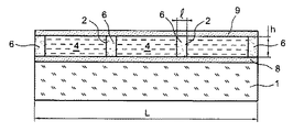
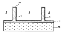
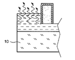
このような光学素子の一例を図1に示す。それは100mm又はそれ以上になり得る幅Wを有する。 An example of such an optical element is shown in FIG. It has a width W that can be 100 mm or more.
それは壁6によって分離された、多くの独立したマイクログルーブ又はマイクロキャビティ2を含む。これらのマイクロキャビティは、曲げやすく平坦な基板上に構築される。壁6及びマイクロキャビティは、集合的なマイクロ技術タイプの方法、又はその構造特性のために選定された樹脂の異方性エッチングによって得ることが出来る。
It includes a number of independent microgrooves or
そしてキャビティは、目的とする光学効果に適した液体4によって満たされ得る。
The cavity can then be filled with a
その後キャビティは、通常壁6の頂上に接着される、曲げやすい材料で作られた閉鎖層9によって閉じられる。
The cavity is then closed by a
全体は、図示された例において、石英のような材料で作られた基板1及びポリマー材料で作られた層8を含む支持体によって形成される。
The whole is formed in the illustrated example by a support comprising a
このような光学素子は、10万から1000万の間であり得る、多数のマイクログルーブを含み得る。 Such an optical element can include a number of microgrooves, which can be between 100,000 and 10 million.
それは壁6を可能な限り見えにくくすることを意味している。このために、20μmから100μmの範囲の樹脂の高さhに対しては、通常2μmから5μmの間の小さい幅wを伴う(図1参照)、高いアスペクト比(又は形状係数)を有する壁を製造することを意味している。
That means making the
しかしこれらの壁の存在は依然として、特に光学素子の透明性に欠陥を起こし、より一般的には、光学素子を通過して形成された画像の品質低下及び/又はその性能低下を起こす。確かに画素を規定する壁は、光を回折することで光と相互作用し、特に透明性低下を引き起こし得る。 However, the presence of these walls still causes defects in the transparency of the optical element, and more generally, the quality of the image formed through the optical element and / or its performance. Indeed, the walls defining the pixels can interact with the light by diffracting the light, and in particular can cause a decrease in transparency.
1つの解決策は、光の一部又は全部を吸収する吸収壁6を製造することであり、それ故に光学素子の透明性欠陥をもたらす回折現象を制限する。
One solution is to produce an
壁は吸収性の感光性材料のダイレクトフォトリソグラフィーによって製造できることが公知であるが、高さhが十分高く、通常20μmを超え、幅wが十分小さい、通常5μm未満である吸収壁を得ることが出来る、商業的に利用可能な材料は見つかっていない。現在、感光性吸収材料及び、それと共に関連したフォトリソグラフィー技術では、得られる壁の高さの最大値は5μm程度であり、それは、依然として期待値を大きく下回っている。 It is known that the wall can be produced by direct photolithography of an absorptive photosensitive material, but it is possible to obtain an absorbing wall whose height h is sufficiently high, usually more than 20 μm, width w is sufficiently small, usually less than 5 μm. There are no commercially available materials that can be used. At present, in the photosensitive absorbing material and the photolithographic technique associated therewith, the maximum value of the obtained wall height is about 5 μm, which is still far below the expected value.
もう1つの解決策は、吸収材料及び/又は吸収粒子をその中に含むことで、既に形成された壁6に吸収性を付与することである。この結果は、ドーピング、拡散又はディッピング技術により得ることが出来る。しかし使用される金属粒子又は顔料が上記で規定した壁の寸法w及びhに対して大きすぎるサイズを有するため、この技術はまだ完全に要求に適合していない。顔料に関しては、エージング問題及びエージングをもたらす吸収性低下が早いという問題もある。
Another solution is to add absorbency to the already formed
従って、キャビティの底部を通常透明に保ち、特に壁が吸収性になるようにできる新規方法が必要である。このような方法は、好ましくは、光学攪乱を制限又は除去できるように、高いアスペクト比を有するキャビティの製造に適合する。 Therefore, there is a need for a new method that can keep the bottom of the cavity normally transparent and in particular make the walls absorbent. Such a method is preferably compatible with the manufacture of cavities with high aspect ratios so that optical disturbances can be limited or eliminated.
もう1つの問題は、反射壁6の製造方法である。これは特に、TFT−LCD移動スクリーンへの応用を考慮する場合である:コントラストを改善するため、スクリーンの内部構造のほんの一部(4−5%)が反射マイクロ構造によって覆われる。このように、たとえスクリーンが直接太陽光に晒された時でも、ユーザーは画像を完璧に識別できる。
Another problem is the manufacturing method of the reflecting
a)支持基板表面に犠牲材料層を形成する段階と、
b)キャビティの底部が前記犠牲材料層によって形成された、前記キャビティの壁を形成する段階と、
c)所定の光学特性を有するいわゆる光学材料の層を、前記壁の頂上、前記壁の側面及び前記キャビティの前記底部に等角的(コンフォーマル)に堆積する段階と、
d)前記犠牲層をエッチングし、この層の前記材料及び前記キャビティの前記底部に存在する前記光学材料の層の前記一部の前記材料を除去する段階と、
を含むマイクロ光学素子のキャビティを形成する方法を開示する。
a) forming a sacrificial material layer on the support substrate surface;
b) forming a cavity wall wherein the bottom of the cavity is formed by the sacrificial material layer;
c) depositing a layer of so-called optical material with predetermined optical properties conformally on the top of the wall, the side of the wall and the bottom of the cavity;
d) etching the sacrificial layer to remove the material of the layer and the material of the portion of the layer of optical material present at the bottom of the cavity;
Disclosed is a method for forming a cavity of a micro-optical element comprising:
光学材料の層は、吸収層又は反射層である。光学材料が吸収性である場合、それは黒色クロム、黒色モリブデン又はアモルファスカーボンを含み得る。 The layer of optical material is an absorption layer or a reflection layer. If the optical material is absorptive, it can include black chrome, black molybdenum or amorphous carbon.
犠牲層の材料は、例えば酸化ケイ素SiO2、窒化ケイ素SiN、酸化インジウムスズ(ITO)、アモルファスカーボン、黒色モリブデン又は黒色クロムを含み得る。 Material of the sacrificial layer, for example silicon oxide SiO 2, silicon nitride SiN, indium tin oxide (ITO), amorphous carbon may include a black molybdenum or black chrome.
犠牲層は、特定のスペクトル領域に対して有利に透明である。 The sacrificial layer is advantageously transparent for certain spectral regions.
段階cで堆積される光学材料の層は、有利に多孔質である。ある実施形態によると、犠牲層をエッチング液が通過するために吸収層の気孔率が十分である場合、犠牲層のエッチングはウェットエッチング液を用いて実施され得る。 The layer of optical material deposited in step c is preferably porous. According to certain embodiments, if the porosity of the absorbing layer is sufficient for the etchant to pass through the sacrificial layer, the sacrificial layer can be etched using a wet etchant.
有利には、段階b)で形成される壁は、10から20の間のアスペクト比(h/w)を有するが、hは支持基板の自由表面より上の壁の高さを示す。 Advantageously, the wall formed in step b) has an aspect ratio (h / w) between 10 and 20, where h denotes the height of the wall above the free surface of the support substrate.
壁は犠牲層の表面に形成され得るが、これは段階cの間まではキャビティ間で連続的であり、段階dの後に、壁は犠牲材料の一部の上に位置する。 The wall can be formed on the surface of the sacrificial layer, which is continuous between the cavities until stage c, and after stage d the wall is located on a part of the sacrificial material.
代わりに、壁の底部は、支持基板自体の上又は中に位置する。 Instead, the bottom of the wall is located on or in the support substrate itself.
−上記の方法の実施を含むこの素子のキャビティを形成する段階と、
−前記素子の前記キャビティの中に1以上の流体を導入する段階と、
−前記キャビティの前記壁の上に閉鎖層を形成する段階と、
を含むマイクロ光学素子を形成する方法を開示する。
-Forming a cavity of this device comprising performing the above method;
Introducing one or more fluids into the cavity of the element;
-Forming a closure layer on the wall of the cavity;
Disclosed is a method for forming a micro-optical element comprising:
壁によって規定されたキャビティを含み、光学材料の層(意味は既に上記で規定済)が壁の頂上及び壁の側面に形成され、キャビティの底部は透明である、マイクロ光学素子を開示する。 Disclosed is a micro-optical element comprising a cavity defined by a wall, wherein a layer of optical material (meaning already defined above) is formed on the top and side of the wall, and the bottom of the cavity is transparent.
ある実施形態によると、各壁の底部は犠牲材料の一部の上に位置し、光学材料の層は犠牲材料のこの部分の側面上にない。 According to one embodiment, the bottom of each wall is located on a portion of the sacrificial material and the layer of optical material is not on the side of this portion of the sacrificial material.
代わりに、各壁(6)の底部は基板上又は基板中に位置し、光学材料の層は基板の表面付近に位置する壁の側面の一部の上にない。 Instead, the bottom of each wall (6) is located on or in the substrate and the layer of optical material is not on the part of the side of the wall located near the surface of the substrate.
各キャビティは少なくとも部分的に流体で満たされ、全てのキャビティは閉鎖層によって閉じられ得る。 Each cavity is at least partially filled with fluid and all cavities can be closed by a closure layer.
光学材料は既に上記に示したように、1以上の特性(吸収性又は反射性、多孔性など)を有し得る。 The optical material may have one or more properties (absorptive or reflective, porous, etc.) as already indicated above.
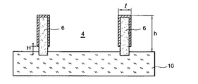
壁は、数μmから数十μm程度、例えば1μmから100μmの間の高さを有し得る。 The wall may have a height on the order of several μm to several tens of μm, for example between 1 μm and 100 μm.
それらは、数μm又はサブミクロン程度、例えば0.5μmから5μmの間の幅を有し得る。 They can have a width on the order of a few μm or submicron, for example between 0.5 μm and 5 μm.
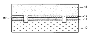
第1の実施形態を図2Aから2Iに関連して示す。 A first embodiment is shown in connection with FIGS. 2A to 2I.
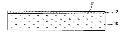
第一に、例えばPETのようなポリマー材料の、ガラス又はシリコンなどの単独の基板10から成り得る支持体が準備される(図2A)。代わりにこれは、固定した支持体上に仮接着によって留められた、例えばポリエチレンテレフタレート“PET”などの曲げやすい層でもよい(後者は図に示していない)。
First, a support is prepared, which can consist of a
このような基板10の平面10’上には、例えば50nmから200nmの間の厚さを有する、いわゆる犠牲材料の平坦層又は平坦膜12が形成される(図2B)。
A flat layer or
この犠牲材料は、マイクロキャビティの壁の下で、最終的なマイクロ素子に依然として存在するため、所望の用途(可視イメージング又は赤外線検出)に応じて可視光線(350-700nm)及び近/中赤外線(0.7-10μm)に対し、有利に透明である。このようにこの層12は透明材料であり、例えば酸化ケイ素SiO2(可視光線に効果的)、窒化ケイ素SiN(1.3から1.55μmの間を除いた近赤外線に効果的)、酸化インジウムスズ(ITO)又はアモルファスカーボン(中赤外線に効果的)などがある。
This sacrificial material is still present in the final microelement under the walls of the microcavity, so depending on the desired application (visible imaging or infrared detection) visible (350-700 nm) and near / mid infrared ( 0.7-10 μm) is advantageously transparent. Thus, this
これらの異なる材料は、例えば蒸発、PVD、PECVD、CVD又はALDなどの方法を用いて堆積され得る。 These different materials can be deposited using methods such as evaporation, PVD, PECVD, CVD or ALD.
透明であろうと吸収性であろうと、犠牲材料12は、好ましくは後にウェット液でエッチングされ得るように選定される。
Whether transparent or absorptive, the
次いで、マイクロキャビティ4の壁6の構造化が実施される。
Then, the structuring of the
予定された応用及び所望の性能に応じて、作動流体の厚さは変化し得る:
−厚さが薄く、マイクロメートル付近である場合は、液晶ディスプレータイプの応用に望ましく、
−厚さが厚く、数十ミクロン程度である場合は、平面回折レンズの場合に望ましい。
Depending on the intended application and the desired performance, the working fluid thickness may vary:
-If the thickness is thin and near micrometer, it is desirable for liquid crystal display type applications,
-If the thickness is large, on the order of several tens of microns, it is desirable for planar diffractive lenses.
このように、もしキャビティに導入されるのに理想的な作動流体の性質が分かっている場合は、壁を製造する際に、基板の自由表面より上に位置する壁の一部の高さhを適合することができる。ある場合は、高さhがマイクロメートル程度、例えば1μmから5μm又は10μmの間の壁を製造することが目的となり、他の場合は、高さが十μm又は数十μm程度、例えば10μmから100μmの間の壁を製造することが目的となる。 Thus, if the nature of the ideal working fluid to be introduced into the cavity is known, the height h of the portion of the wall located above the free surface of the substrate when manufacturing the wall Can be adapted. In some cases, the purpose is to produce a wall with a height h on the order of micrometers, for example between 1 μm and 5 μm or 10 μm, in other cases the height is on the order of 10 μm or several tens of μm, for example 10 μm to 100 μm The purpose is to produce a wall between.
その高さが1μm程度の厚さ(通常1μmから10μmの間)の壁の場合は、例えばマイクロ鋳造、スクリーンプリンティング、フォトリソグラフィー、プラズマエッチングなどのような幾つかの技術が実施され得る。 In the case of a wall whose height is as high as 1 μm (usually between 1 μm and 10 μm), several techniques such as microcasting, screen printing, photolithography, plasma etching etc. can be implemented.
より高い高さの場合(通常10μmから100μmの間)、例えば特に厚い樹脂のフォトリソグラフィーによって、1ミクロン程度及び通常5μmより低い、例えば1μmから5μmの間などの十分低い壁の幅wが得られる。つまりこの場合、フォトリソグラフィー技術がプラズマエッチング技術に比べて、有利に好ましい。このようにこのフォトリソグラフィー技術は、比較的高い高さ、例えば10から20の間などの大きいアスペクト比を有する壁を得ることが出来る。 For higher heights (usually between 10 μm and 100 μm), for example, particularly thick resin photolithography gives a sufficiently low wall width w of around 1 micron and usually lower than 5 μm, for example between 1 μm and 5 μm. . In other words, in this case, the photolithography technique is advantageous over the plasma etching technique. Thus, this photolithography technique can obtain walls having a relatively high height, for example a large aspect ratio such as between 10 and 20.
後者の技術の典型的な実施の一例を図2C及び2Dに示す:厚い感光性樹脂18が犠牲層12に堆積される。そしてこの樹脂は適切なマスクで覆われ(図2D)、その後ミクロ電子工学において一般に使用される技術に応じて現像される。
An example of a typical implementation of the latter technique is shown in FIGS. 2C and 2D: a thick
キャビティ4の壁6はこうして得られる。それらは基板上の平坦面10’及び犠牲層12に対して概して垂直である。後者はこの壁形成操作によって、ほとんど又は全く影響を受けない。
The
これは結果として、連続的かつ平坦であり、壁6の下まで延長された層12を含む構造となる(図2D)。後者は、例えば10から20の間の高いアスペクト比h/wを有し得る。幅wが2μmから5μmの間である場合、得られる壁の高さhは20μmから100μmの間であり得る。しかし既に上記で示したように、異なる幾何学的特性を有する壁及び特に低い高さの壁、例えば10μmより低い壁なども、本願で開示した方法によって得ることが出来る。
This results in a structure that includes a
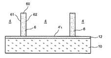
そして素子全体に(図2E)、厚さが通常50nmから500nmの間であり、なお所望の応用に応じて可視光線及び/又は近赤外線及び/又は中赤外線を吸収する材料である、等角層30が堆積される。この層は光の一部又は全部を吸収でき、光学素子の透明性低下をもたらす回折現象を制限できる。好ましくは、可視スペクトル領域に対してはアモルファスカーボン又は黒色クロム/モルブデンが選定され、あるいは近赤外線及び/又は中赤外線に対してはナノ結晶ダイヤモンドが選定される。 And the entire device (FIG. 2E) is a conformal layer that is typically between 50 nm and 500 nm in thickness and is still a material that absorbs visible and / or near infrared and / or mid-infrared depending on the desired application. 30 is deposited. This layer can absorb some or all of the light and limit diffraction phenomena that lead to reduced transparency of the optical element. Preferably, amorphous carbon or black chrome / malbden is selected for the visible spectral region, or nanocrystalline diamond is selected for the near infrared and / or mid infrared.
この層は適用され、壁6の頂上60、壁の側面61,62及びキャビティの底部4’1を連続的に覆う。
This layer is applied and continuously covers the top 60 of the
例えば、ナノ結晶ダイヤモンド層はプラズマアシスト化学蒸着(PACVD)、黒色モリブデン層は化学蒸着(CVD)、黒色クロム層は物理蒸着(PVD)又は電子ビーム蒸発を用いて、好ましくは堆積される。 For example, the nanocrystalline diamond layer is preferably deposited using plasma assisted chemical vapor deposition (PACVD), the black molybdenum layer using chemical vapor deposition (CVD), and the black chromium layer using physical vapor deposition (PVD) or electron beam evaporation.
好ましくは、この吸収層30は、ウェットエッチング液が吸収層を通過して犠牲層12をエッチングできるように十分な気孔率を有する。そして、気孔率が10%より低い範囲では無孔層と判断せれ、10%から50%の範囲では多孔層と判断される。この気孔率はまた、堆積パラメータによって調整され得る。例えば、冷たい基板上に“電子ビーム蒸発”によって堆積された黒色クロム層は40%程度の気孔率を有するが、堆積中に基板が熱せられると(300℃)、この気孔率は16%まで低下する。
Preferably, the absorbing
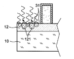
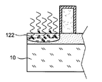
こうして犠牲層12のウェットエッチングは、例えば酸又は塩基のエッチングなどによって、その次に実施される(図2F)。好ましくは、キャビティの底部4’1に存在する吸収層30の気孔率は、犠牲層12をエッチングし、キャビティの底部にある吸収層30をいわゆる“リフトオフ”効果によって引き抜けるように調整される。
Thus, the wet etching of the
この段階を図3Aから3Dにおいて、より詳細に示す。キャビティの底部にある吸収層30の一部が上昇するようにエッチングが十分進むまで(図3D)、エッチング液は犠牲層12をエッチングするために、その気孔31を通って吸収層30の下を進む(図3Bと3C)。このように上昇されてエッチング液17と混合された相当量の吸収材料は、こうして後者を引き抜く間に除去される(図3D)。これらの図から分かるように、液17は気孔31を通って層12の材料を徐々にエッチングし、そのエッチング領域は図3A-3Cにおいて参照120,121,122によって指定されているが、その大きさは、その工程が進むにつれて増大する。
This stage is shown in more detail in FIGS. 3A to 3D. Until etching proceeds sufficiently so that a part of the
最終的に(図2F)、壁6の頂上60及び壁6の側面61,62は依然として、吸収材料30によって覆われる。壁6の下には、壁6と同じ幅を有する犠牲層の残存部分12’があり、層30は、この層12’の厚さと実質的に同一又は近い高さにおいて、この部分12’の側面12’1,12’2を覆わない。こうして形成されたキャビティ4の底部4’は、材料12から取り除かれる。
Eventually (FIG. 2F), the top 60 of the
エッチング液17は、ちょうど堆積された吸収層及び壁6をエッチングしないように、吸収層30を構成する材料及び壁6を構成する材料にも選択的であるように選ばれる。従って、例えば二酸化ケイ素SiO2の犠牲層12、黒色クロムの吸収層30、及びゾルゲル有機ケイ素材料の壁6である場合、エッチング液は、フッ化アンモニウム(NH4F)で緩衝化され、部分的に希釈されたフッ化水素酸(HF)となる。
The
ウェットエッチングはまた、壁6の下をオーバーエッチングすることで“リフトオフ”効果を壁にまで広げないように制御される。もしエッチングが高すぎると、層12のエッチング領域はやはり壁6の下に形成され、それは安定性を失う。このために、ウェット液によるエッチング時間は制御される。犠牲層12は、例えば100nmから250nm程度の幅を有し、壁は2μmから5μmであり得る厚さを有する。これに関して、壁は層12の厚さの10から50倍大きい幅を有し得る。たとえサイドエッチング(壁の下)が垂直エッチング(吸収層の下)と同等程度の速度で起こると仮定しても、サイドエッチングは、吸収層が既にエッチングされたという時に、十分早く停止され得る。
Wet etching is also controlled so as not to spread the “lift-off” effect to the wall by over-etching under the
もう1つの壁形成方法を伴った、代替案の実施形態を、図4Aから4Gに関連して以下に示す。 An alternative embodiment with another wall formation method is shown below in connection with FIGS. 4A to 4G.
基板10及びその犠牲層を伴う図2Bの形態から開始して、ハードマスク層16(例えば、50nm厚のクロム層)が堆積され、続いて樹脂のマスク17(図4A)が堆積される。それは後に形成される壁の位置及びその幅を規定し、犠牲層と同時に場合によっては基板10の一部もエッチングすることを可能にする。そしてこれらの層16,17のエッチング領域に壁が形成される。基板10の材料のエッチングが持続される場合、後に形成される壁6(図4B)の機械抵抗が高められる。
Starting with the configuration of FIG. 2B with the
そして樹脂18(図4C)が塗られる。それは、場合によっては基板10内部も含めたエッチング領域に浸透する。前記の実施形態とは異なり、犠牲層は全基板10の上で不連続になる。
Resin 18 (FIG. 4C) is then applied. In some cases, it penetrates into the etching region including the inside of the
そしてマイクロキャビティの壁6は、例えば既に上記したうちの何れか1つの方法を用いて、この樹脂18(図4D)の中に形成される。その後、その層12に選択的で、出来る限り層12に影響を与えない、好ましくはソフトな方法によって、マスク層17及びハードマスク層16は除去される(図4E)。この方法は、例えば界面活性剤BE30:1を伴ったHFエッチングであり、それによって良好な結果が得られる。
The
そして全体の素子上に等角層30が堆積されるが(図4F)、その性質、気孔率、並びに光学及び厚み特性は、特に図2Eに関連して、既に前記に記載した。再びこの層は適用され、犠牲層12と同時に壁6の頂上60及び壁の側面61,62も連続的に覆う。
A
そして、犠牲層12のウェットエッチングは、例えば酸又は塩基のエッチングによって実施される(図4G)。図2Fの場合と同様に、キャビティの底部4’1に存在する吸収層30の気孔率は、好ましくは犠牲層12をエッチングし、キャビティの底部にある吸収層30をいわゆる“リフトオフ”効果によって引き抜けるように調整される。再び、層30の気孔31を通るエッチング機構及びエッチング液の選択に関しては、上記の説明が参照され得る(図3A-3C)。
The wet etching of the
最終的に(図4G)、壁6の頂上60及び側面61,62は依然として、吸収材料30によって覆われる。今回、壁6の下に犠牲層の残存部分はないが、層30は、基板10の自由表面と層30の底部の間に位置する、壁の側面61,62のより低い部分を覆っておらず、その高さHは実質的に前記層12の厚さと同等、又は前記層12と層30の厚さの合計と同程度である。
Finally (FIG. 4G), the top 60 and the
上記の製造方法は、吸収特性を有する層30を伴って記載されている。しかし代わりに、この層は反射特性を有することもあり、コントラストを改善するためにスクリーンの内部構造のほんの一部(4-5%)が反射マイクロ構造によって覆われるので、それはTFT−LCD移動スクリーンを製造する際に興味深くなり得る:このように、たとえスクリーンが直接太陽光に晒された時でも、ユーザーは画像を完璧に識別できる。反射壁を有するキャビティの製造方法は、吸収壁に対する方法と類似している。
The above manufacturing method is described with a
いずれにしても、吸収性又は反射性という特定の光学特性を有する材料の層30で覆われた壁6によって規定されたキャビティ4を含む構造が得られる。図2Fでは、壁6の下に材料の残存部分12’が見られる。壁6は基板10の自由表面より上の部分である高さhを有し、それは数μmから数十μm程度、例えば10μmより高く、更に例えば5μmから50μmの間であり得る。それらの幅wは、数μm又はサブミクロン程度、例えば5μmより低く、あるいは5μmから0.5μmの間であり得る。これらの幾何学パラメータに対する他の値の範囲は、既に上記において記載してある。
In any case, a structure is obtained that includes a
そして1以上のキャビティの充填は、キャビティ4内部に対して装置E(図5A)を用い、数ピコリットル程度であり得る体積を有する噴流又は液滴26として液体24を発射することで行われ得る。液体は数十から数百ピコリットルである低容量配置の使用に適した技術を用いて送られ得る。用いられる装置Eは、インクジェットディスペンシングの何れか1つに類似した液体分配技術を実施できる。
The filling of one or more cavities can then be performed by using the device E (FIG. 5A) into the
液体材料24は、部分的又は完全にキャビティ4を満たせる。キャビティの完全充填は、壁6の頂上62に到達するように行われ得る。
The
結果物は、支持体10の材料と同一であろうとなかろうと、プラスチックフィルムのような保護フィルム9を設ける(最も簡単にはラミネートする)ことで完了される(図5B)。このフィルムは場合によっては、最終的な機能(防眩、ハード層、防汚など)のために考案された機能層によって覆われる。
The result is completed by providing (most simply laminating) a
図5A及び5Bは、図2Fの構造で作られる部品の場合に関連するが、もう1つの部品もまた上記で説明したように、キャビティを満たし保護フィルム9を設けることによって、図4Gの構造から得ることが出来る。
FIGS. 5A and 5B relate to the case of a part made with the structure of FIG. 2F, but the other part can also be removed from the structure of FIG. 4G by filling the cavity and providing a
最終結果物のカスタマイズは、例えばガラスレンズとして最終的な表面の上にそれを設ける前に行われ得る。このカスタマイズは、要求されなくても、スタックを製造するのに使用される固定した支持体に、有利に実施され得る。支持体を製造する際にカスタマイズする場合は、レーザーや超音波、又は切削工具を用いて製造され得る。物体表面のプレシールを保証し、最適なシーリングのための薄片の良好な表面条件、及び工業化に適した高速遂行を保証するような品質を有する技術が好ましい。このカスタマイズは、ガス厚及び耐水性、結果物の寿命を通じた機械抵抗、消費財(必要ならば、例としてガラスがある)に適した見栄えを保証する表面シーリングを伴う。 The customization of the final product can be done before providing it on the final surface, for example as a glass lens. This customization can be advantageously performed on a fixed support used to manufacture the stack, even if not required. When customizing when manufacturing the support, it can be manufactured using laser, ultrasound, or cutting tools. A technique having a quality that ensures pre-sealing of the object surface, good surface conditions of the flakes for optimal sealing, and high speed performance suitable for industrialization is preferred. This customization involves gas sealing and water resistance, mechanical resistance throughout the life of the resulting product, and surface sealing that ensures a suitable appearance for consumer goods (eg glass if necessary).
4 キャビティ
4’1 底部
6 壁
10 基板
10’ 平面
12 犠牲材料層
12’ 残存部分
12’1,12’2 側面
16 ハードマスク層
17 マスク
18 感光性樹脂
24 液体
26 液滴
30 光学材料の層
31 気孔
60 頂上
61,62 側面
120,121,122 エッチング領域
4 Cavity 4'1
Claims (18)
b)キャビティ(4)の底部が前記犠牲材料層によって形成された、前記キャビティの壁(6)を形成する段階と、
c)所定の光学特性を有し、多孔質材料である、いわゆる光学材料の層(30)を、前記壁の頂上(60)、前記壁の側面(61,62)及び前記キャビティの前記底部(4’)に等角的に堆積する段階と、
d)前記犠牲層(12)をエッチングし、この層の前記材料及び前記キャビティ(4)の前記底部に存在する前記光学材料の層(30)の一部の前記材料を除去する段階と、
を含むマイクロ光学素子のキャビティ(4)を形成する方法。 a) forming a sacrificial material layer (12) on the surface of the support substrate (10);
b) forming a cavity wall (6) in which the bottom of the cavity (4) is formed by the sacrificial material layer;
c) a so-called layer of optical material (30), which has a predetermined optical property and is a porous material; 4 ′) conformally depositing;
d) etching the sacrificial layer (12) to remove the material of this layer and part of the layer of optical material (30) present at the bottom of the cavity (4);
Forming a cavity (4) of a micro-optical element comprising:
−前記素子の前記キャビティ(4)の中に1以上の流体を導入する段階と、
−前記キャビティの前記壁の上に閉鎖層(9)を形成する段階と、
を含むマイクロ光学素子を形成する方法。 Forming the cavity (4) of the device, comprising performing the method according to any one of claims 1 to 9;
Introducing one or more fluids into the cavity (4) of the element;
-Forming a closure layer (9) on the wall of the cavity;
A method of forming a micro-optical element comprising:
Applications Claiming Priority (2)
| Application Number | Priority Date | Filing Date | Title |
|---|---|---|---|
| FR1055944A FR2963112B1 (en) | 2010-07-21 | 2010-07-21 | WALL MICROSTRUCTURE WITH DETERMINED OPTICAL PROPERTIES AND METHOD FOR PRODUCING MICROSTRUCTURES |
| FR1055944 | 2010-07-21 |
Publications (1)
| Publication Number | Publication Date |
|---|---|
| JP2012024917A true JP2012024917A (en) | 2012-02-09 |
Family
ID=43755087
Family Applications (1)
| Application Number | Title | Priority Date | Filing Date |
|---|---|---|---|
| JP2011158777A Pending JP2012024917A (en) | 2010-07-21 | 2011-07-20 | Microstructure with wall of determined optical property and method for making microstructure |
Country Status (4)
| Country | Link |
|---|---|
| US (1) | US9116269B2 (en) |
| EP (1) | EP2410373A1 (en) |
| JP (1) | JP2012024917A (en) |
| FR (1) | FR2963112B1 (en) |
Cited By (1)
| Publication number | Priority date | Publication date | Assignee | Title |
|---|---|---|---|---|
| JP2019514194A (en) * | 2015-12-29 | 2019-05-30 | ルミレッズ ホールディング ベーフェー | Flip chip LED with side reflector and phosphor |
Families Citing this family (1)
| Publication number | Priority date | Publication date | Assignee | Title |
|---|---|---|---|---|
| US11424396B2 (en) * | 2015-12-29 | 2022-08-23 | Lumileds Llc | Flip chip LED with side reflectors and phosphor |
Citations (5)
| Publication number | Priority date | Publication date | Assignee | Title |
|---|---|---|---|---|
| JP2000124469A (en) * | 1998-10-13 | 2000-04-28 | Toyota Central Res & Dev Lab Inc | Micro-closed container and method for producing the same |
| JP2006326806A (en) * | 2005-05-30 | 2006-12-07 | Toshiba Corp | Semiconductor device using MEMS technology |
| US20090109515A1 (en) * | 2007-10-30 | 2009-04-30 | Spatial Photonics, Inc. | Encapsulated spatial light modulator having large active area |
| US20100006957A1 (en) * | 2008-06-06 | 2010-01-14 | Taiwan Semiconductor Manufacturing Company, Ltd. | Microscopic structure packaging method and device with packaged microscopic structure |
| JP2010044375A (en) * | 2008-07-15 | 2010-02-25 | Commissariat A L'energie Atomique | Liquid crystal alignment layer deposited and rubbed before creating microstructure |
Family Cites Families (48)
| Publication number | Priority date | Publication date | Assignee | Title |
|---|---|---|---|---|
| US3978580A (en) | 1973-06-28 | 1976-09-07 | Hughes Aircraft Company | Method of fabricating a liquid crystal display |
| US3863249A (en) | 1973-07-30 | 1975-01-28 | Motorola Inc | Magnetic fluid display device |
| CH591090A5 (en) | 1976-03-29 | 1977-09-15 | Wenger Jean Sebastien | Thin-edged lens for focussing solar rays in heater - with liquid-filled transparent or translucent shell |
| US4989226A (en) | 1987-08-21 | 1991-01-29 | Brigham Young University | Layered devices having surface curvature |
| US5417801A (en) | 1993-06-29 | 1995-05-23 | Xerox Corporation | Process to manufacture bushings for micromechanical elements |
| JP3821315B2 (en) * | 1995-11-13 | 2006-09-13 | シャープ株式会社 | Liquid crystal display device and manufacturing method thereof |
| KR970048809A (en) | 1995-12-30 | 1997-07-29 | 손욱 | LCD with Elastic Adhesive Spacers |
| EP0785565A1 (en) * | 1996-01-22 | 1997-07-23 | Hitachi Chemical Co., Ltd. | Phosphor pattern, processes for preparing the same and photosensitive element to be used for the same |
| US6266121B1 (en) * | 1996-11-28 | 2001-07-24 | Sharp Kabushiki Kaisha | Liquid crystal display element and method of manufacturing same |
| ATE208828T1 (en) | 1998-03-06 | 2001-11-15 | Novozymes As | A SCREENING METHOD BASED ON FLUORESCENCE POLARIZATION |
| US6063653A (en) | 1998-07-07 | 2000-05-16 | Industrial Technology Research Institute | Method of fabricating a TFT-LCD |
| US6183917B1 (en) | 1998-07-31 | 2001-02-06 | Canon Kabushiki Kaisha | Color filter, production process of color filter, liquid crystal display device using the color filter, and production process of black matrix |
| US6947202B2 (en) | 2000-03-03 | 2005-09-20 | Sipix Imaging, Inc. | Electrophoretic display with sub relief structure for high contrast ratio and improved shear and/or compression resistance |
| US6829078B2 (en) | 2000-03-03 | 2004-12-07 | Sipix Imaging Inc. | Electrophoretic display and novel process for its manufacture |
| TW556044B (en) | 2001-02-15 | 2003-10-01 | Sipix Imaging Inc | Process for roll-to-roll manufacture of a display by synchronized photolithographic exposure on a substrate web |
| JP2002323630A (en) | 2001-04-25 | 2002-11-08 | Ntt Advanced Technology Corp | Method and apparatus for manufacturing optical circuit by liquid ejector |
| WO2002088671A1 (en) | 2001-04-26 | 2002-11-07 | Esytech Ab | A separation unit, a method for separation, and a device for mounting a separation unit in a separation apparatus |
| US6635306B2 (en) * | 2001-06-22 | 2003-10-21 | University Of Cincinnati | Light emissive display with a black or color dielectric layer |
| TWI308231B (en) | 2001-08-28 | 2009-04-01 | Sipix Imaging Inc | Electrophoretic display |
| JP2003177232A (en) | 2001-10-02 | 2003-06-27 | Seiko Epson Corp | Color filter, method of manufacturing the same, display device, and electronic device |
| US6962822B2 (en) | 2002-08-07 | 2005-11-08 | International Business Machines Corporation | Discrete nano-textured structures in biomolecular arrays, and method of use |
| EP1554632B1 (en) * | 2002-10-21 | 2011-08-24 | Canon Kabushiki Kaisha | Process for producing electrophoretic display devices |
| US6958207B1 (en) | 2002-12-07 | 2005-10-25 | Niyaz Khusnatdinov | Method for producing large area antireflective microtextured surfaces |
| FR2848303B1 (en) | 2002-12-09 | 2005-03-04 | Commissariat Energie Atomique | OPTICAL ARRANGEMENT WITH TWO OPTICAL INPUTS / OUTPUTS AND A METHOD OF MANUFACTURING |
| GB2435717B (en) | 2003-09-04 | 2008-03-26 | Hitachi Ltd | Active matrix display device |
| US7067355B2 (en) | 2004-05-26 | 2006-06-27 | Hewlett-Packard Development Company, L.P. | Package having bond-sealed underbump |
| KR101234173B1 (en) | 2004-07-02 | 2013-02-19 | 에씰로아 인터내셔날/콩파니에 제네랄 도프티크 | Method for producing a transparent optical element, an optical component involved into said method and the thus obtained optical element |
| FR2872589B1 (en) | 2004-07-02 | 2006-10-27 | Essilor Int | METHOD FOR PRODUCING A TRANSPARENT OPTICAL ELEMENT, OPTICAL COMPONENT INVOLVED IN THIS METHOD AND OPTICAL ELEMENT THUS OBTAINED |
| US20060139529A1 (en) | 2004-08-31 | 2006-06-29 | Shie-Chang Jeng | Manufacturing method for a transflective liquid crystal display device |
| CN104925744A (en) | 2004-11-04 | 2015-09-23 | 微芯片生物技术公司 | Compression And Cold Weld Sealing Methods And Devices |
| EP1672394B1 (en) | 2004-12-16 | 2007-04-18 | Ecole d'Ingénieurs ARC | Method for producing a device having a plastic membrane and device so manufactured |
| FR2879757B1 (en) | 2004-12-17 | 2007-07-13 | Essilor Int | METHOD FOR PRODUCING A TRANSPARENT OPTICAL ELEMENT, OPTICAL COMPONENT INVOLVED IN THIS METHOD AND OPTICAL ELEMENT THUS OBTAINED |
| WO2006067650A1 (en) | 2004-12-20 | 2006-06-29 | Koninklijke Philips Electronics N.V. | Method of manufacturing an electrophoretic display device and electrophoretic display device |
| US9229222B2 (en) | 2005-02-23 | 2016-01-05 | Pixtronix, Inc. | Alignment methods in fluid-filled MEMS displays |
| EP1885839B1 (en) | 2005-04-26 | 2018-08-08 | Life Technologies Corporation | Systems and methods for multiple analyte detection |
| EP1722424A1 (en) | 2005-05-13 | 2006-11-15 | Université Libre de Bruxelles | Method for the manufacturing of homeotropically aligned layer of discotic liquid crystals |
| TWI288116B (en) | 2005-06-07 | 2007-10-11 | Chien-Chung Fu | Method of manufacturing a LIGA mold by backside exposure |
| FR2888953B1 (en) | 2005-07-20 | 2008-02-08 | Essilor Int | PIXELLIZED OPTIC COMPONENT WITH APODIZED WALLS, METHOD FOR MANUFACTURING THE SAME AND USE THEREOF IN THE MANUFACTURE OF A TRANSPARENT OPTICAL ELEMENT |
| FR2888948B1 (en) | 2005-07-20 | 2007-10-12 | Essilor Int | PIXELLIZED TRANSPARENT OPTIC COMPONENT COMPRISING AN ABSORBENT COATING, METHOD FOR PRODUCING THE SAME AND USE THEREOF IN AN OPTICAL ELEMENT |
| US7399421B2 (en) | 2005-08-02 | 2008-07-15 | International Business Machines Corporation | Injection molded microoptics |
| GB2432966A (en) | 2005-11-25 | 2007-06-06 | Seiko Epson Corp | Dye-sensitised electrochemical cell |
| US7136216B1 (en) | 2005-12-15 | 2006-11-14 | Palo Alto Research Center Incorporated | Dual-stage tape-sealing of microcells or channels for display applications |
| FR2897164B1 (en) | 2006-02-09 | 2008-03-14 | Commissariat Energie Atomique | REALIZING CAVITIES THAT CAN BE FILLED BY A FLUID MATERIAL IN AN OPTICAL MICROTECHNOLOGICAL COMPOUND |
| GB0611141D0 (en) | 2006-06-07 | 2006-07-19 | Univ Strathclyde | Multistable reflective liquid crystal device |
| US8512581B2 (en) * | 2006-10-09 | 2013-08-20 | Solexel, Inc. | Methods for liquid transfer coating of three-dimensional substrates |
| FR2933205B1 (en) | 2008-06-27 | 2010-08-13 | Commissariat Energie Atomique | IMPROVED METHOD FOR MAKING LIQUID-FILLED ENCLOSURES AND CLOSED BY A MEMBRANE |
| JP5609700B2 (en) * | 2011-02-17 | 2014-10-22 | ソニー株式会社 | Electrophoretic element and display device |
| JP5741122B2 (en) * | 2011-03-28 | 2015-07-01 | ソニー株式会社 | Electrophoretic element, display device and electronic device |
-
2010
- 2010-07-21 FR FR1055944A patent/FR2963112B1/en not_active Expired - Fee Related
-
2011
- 2011-07-20 US US13/186,940 patent/US9116269B2/en not_active Expired - Fee Related
- 2011-07-20 JP JP2011158777A patent/JP2012024917A/en active Pending
- 2011-07-20 EP EP20110174613 patent/EP2410373A1/en not_active Withdrawn
Patent Citations (5)
| Publication number | Priority date | Publication date | Assignee | Title |
|---|---|---|---|---|
| JP2000124469A (en) * | 1998-10-13 | 2000-04-28 | Toyota Central Res & Dev Lab Inc | Micro-closed container and method for producing the same |
| JP2006326806A (en) * | 2005-05-30 | 2006-12-07 | Toshiba Corp | Semiconductor device using MEMS technology |
| US20090109515A1 (en) * | 2007-10-30 | 2009-04-30 | Spatial Photonics, Inc. | Encapsulated spatial light modulator having large active area |
| US20100006957A1 (en) * | 2008-06-06 | 2010-01-14 | Taiwan Semiconductor Manufacturing Company, Ltd. | Microscopic structure packaging method and device with packaged microscopic structure |
| JP2010044375A (en) * | 2008-07-15 | 2010-02-25 | Commissariat A L'energie Atomique | Liquid crystal alignment layer deposited and rubbed before creating microstructure |
Cited By (1)
| Publication number | Priority date | Publication date | Assignee | Title |
|---|---|---|---|---|
| JP2019514194A (en) * | 2015-12-29 | 2019-05-30 | ルミレッズ ホールディング ベーフェー | Flip chip LED with side reflector and phosphor |
Also Published As
| Publication number | Publication date |
|---|---|
| EP2410373A1 (en) | 2012-01-25 |
| US9116269B2 (en) | 2015-08-25 |
| FR2963112B1 (en) | 2013-02-15 |
| US20120019922A1 (en) | 2012-01-26 |
| FR2963112A1 (en) | 2012-01-27 |
Similar Documents
| Publication | Publication Date | Title |
|---|---|---|
| EP1982217B1 (en) | Production of cavities that can be filled with a fluid material in an optical microtechnological component | |
| US9217086B2 (en) | Method of fabricating transparent anti-reflective article | |
| CN110989063B (en) | A color filter based on rectangular lattice arrangement and its preparation method and application | |
| CN115421295B (en) | Design method of superlens, superlens and processing technology | |
| EP2407416B1 (en) | Method for manufacturing a membrane device retaining a fluid | |
| JP2024023395A (en) | Methods of manufacturing optical devices and resulting optical devices | |
| CN114488365A (en) | Far infrared superlens and processing method thereof | |
| JP6060620B2 (en) | Manufacturing method of microlens array | |
| CN103048715A (en) | Planar sub-wavelength aperiodic high-contrast grating and preparation method thereof | |
| US12498581B2 (en) | Air pocket structures for promoting total internal reflection in a waveguide | |
| CN107121715A (en) | A kind of super surface perfect absorbeperfect absorber of large-area wide incidence angle based on coupling Michaelis resonance and preparation method thereof | |
| US20100014036A1 (en) | Alignment layer of liquid crystals deposited and rubbed before making microstructures | |
| US9156216B2 (en) | Process for manufacturing a segmented optical structure | |
| JP5248869B2 (en) | Method for filling a cavity in an optical microtech compound with a fluid material | |
| JP2012024917A (en) | Microstructure with wall of determined optical property and method for making microstructure | |
| CN102738698A (en) | Production method of deep submicron etched groove based on ultraviolet lithography process | |
| JPH03115139A (en) | Antireflection film and its formation | |
| CN1405366A (en) | Method for preparing air ball titanium dioxide photonic crystal of purple light wave band | |
| EP4336226B1 (en) | Method for producing anti-reflective textured surface using additive thin film | |
| US20070267057A1 (en) | Optical device and method of forming the same | |
| KR102891211B1 (en) | Anti-reflective nanostructure and method of manufacturing the same | |
| WO2022197712A1 (en) | Airgap structures for improved eyepiece efficiency | |
| CN120722598A (en) | A control substrate and spatial light modulator | |
| CN1248019C (en) | Fabrication method of MEMS Fabry-Perot device |
Legal Events
| Date | Code | Title | Description |
|---|---|---|---|
| A621 | Written request for application examination |
Free format text: JAPANESE INTERMEDIATE CODE: A621 Effective date: 20140701 |
|
| A977 | Report on retrieval |
Free format text: JAPANESE INTERMEDIATE CODE: A971007 Effective date: 20150824 |
|
| A131 | Notification of reasons for refusal |
Free format text: JAPANESE INTERMEDIATE CODE: A131 Effective date: 20150914 |
|
| A02 | Decision of refusal |
Free format text: JAPANESE INTERMEDIATE CODE: A02 Effective date: 20160229 |