JP2012018869A - Electric contact - Google Patents
Electric contact Download PDFInfo
- Publication number
- JP2012018869A JP2012018869A JP2010156594A JP2010156594A JP2012018869A JP 2012018869 A JP2012018869 A JP 2012018869A JP 2010156594 A JP2010156594 A JP 2010156594A JP 2010156594 A JP2010156594 A JP 2010156594A JP 2012018869 A JP2012018869 A JP 2012018869A
- Authority
- JP
- Japan
- Prior art keywords
- contact
- radius
- tip
- ridges
- pair
- Prior art date
- Legal status (The legal status is an assumption and is not a legal conclusion. Google has not performed a legal analysis and makes no representation as to the accuracy of the status listed.)
- Pending
Links
Images


Classifications
-
- H—ELECTRICITY
- H01—ELECTRIC ELEMENTS
- H01R—ELECTRICALLY-CONDUCTIVE CONNECTIONS; STRUCTURAL ASSOCIATIONS OF A PLURALITY OF MUTUALLY-INSULATED ELECTRICAL CONNECTING ELEMENTS; COUPLING DEVICES; CURRENT COLLECTORS
- H01R13/00—Details of coupling devices of the kinds covered by groups H01R12/70 or H01R24/00 - H01R33/00
- H01R13/02—Contact members
- H01R13/22—Contacts for co-operating by abutting
- H01R13/24—Contacts for co-operating by abutting resilient; resiliently-mounted
- H01R13/2407—Contacts for co-operating by abutting resilient; resiliently-mounted characterized by the resilient means
-
- H—ELECTRICITY
- H01—ELECTRIC ELEMENTS
- H01R—ELECTRICALLY-CONDUCTIVE CONNECTIONS; STRUCTURAL ASSOCIATIONS OF A PLURALITY OF MUTUALLY-INSULATED ELECTRICAL CONNECTING ELEMENTS; COUPLING DEVICES; CURRENT COLLECTORS
- H01R12/00—Structural associations of a plurality of mutually-insulated electrical connecting elements, specially adapted for printed circuits, e.g. printed circuit boards [PCB], flat or ribbon cables, or like generally planar structures, e.g. terminal strips, terminal blocks; Coupling devices specially adapted for printed circuits, flat or ribbon cables, or like generally planar structures; Terminals specially adapted for contact with, or insertion into, printed circuits, flat or ribbon cables, or like generally planar structures
- H01R12/70—Coupling devices
- H01R12/71—Coupling devices for rigid printing circuits or like structures
- H01R12/712—Coupling devices for rigid printing circuits or like structures co-operating with the surface of the printed circuit or with a coupling device exclusively provided on the surface of the printed circuit
- H01R12/714—Coupling devices for rigid printing circuits or like structures co-operating with the surface of the printed circuit or with a coupling device exclusively provided on the surface of the printed circuit with contacts abutting directly the printed circuit; Button contacts therefore provided on the printed circuit
Abstract
Description
本発明は、回路基板の導体パターンや相手コンタクトといった導電性を有する被接触物に接触する電気コンタクトに関する。 The present invention relates to an electrical contact that contacts a contacted object having conductivity such as a conductor pattern of a circuit board or a mating contact.
従来より、回路基板の導体パターンや相手コンタクトといった導電性を有する被接触物に接触する電気コンタクトと、電気コンタクトを支持する絶縁性のハウジングを備えた電気コネクタが知られている。
この電気コネクタの一例として、例えば、図7に示すICソケットが知られている(特許文献1参照)。図7は、従来のICソケットを示し、(A)はICパッケージのリードとICソケットのコンタクトが接続した状態の部分断面図、(B)はコンタクトの凹凸条部分を拡大して示す部分拡大図である。
2. Description of the Related Art Conventionally, an electrical connector is known that includes an electrical contact that contacts a contacted object having conductivity such as a conductor pattern of a circuit board or a mating contact, and an insulating housing that supports the electrical contact.
As an example of this electrical connector, for example, an IC socket shown in FIG. 7 is known (see Patent Document 1). 7A and 7B show a conventional IC socket, in which FIG. 7A is a partial cross-sectional view showing a state where an IC package lead and an IC socket contact are connected, and FIG. 7B is an enlarged partial enlarged view showing an uneven portion of the contact. It is.
図7(A)に示すICソケット101は、ICパッケージ130の配列されたリード131と接触する少なくとも1列の導電性を有するコンタクト120と、コンタクト120を支持する絶縁性のハウジング110とを備えている。ハウジング110には、ICパッケージ130が載置される。そして、ICソケット101のハウジング110にICパッケージ130を載置したときに、コンタクト120の接触部121は、リード131と互いに図7(B)に示す矢印W方向にワイピングして接触する。
The
そして、各コンタクト120の接触部121のリード131との接触面122には、ワイピング方向(矢印W方向)と直交する方向に延びる複数の凹凸条123が設けられている。この凹凸条123は、接触面122から凹む複数のV字形の溝123aと、これら溝123aの両側に溝123aに沿う複数対の凸条123bとを備えている。凹凸条123は、ワイピング方向と直交する方向(図7(B)における紙面と直交する方向)に、ドラッギングによって形成される。
The
そして、これら凹凸条123の寸法として、例えば、溝123aの角度α1が60度、深さh1が0.08mm、凸条123b間の距離d1が0.09mm、溝123aの断面積Sが0.037mm2、溝123a、123a間の距離D1が0.020mmとされている。
このような凹凸条123を設けることにより、コンタクト120とリード131との接触時にワイピング量が少なくても、伸びる性質を有する異物を凹凸条36で掻き取って除去し、確実に電気的接続を行うことができる。
Then, as the dimension of these concave-convex 123, for example, the angle alpha 1 is 60 degrees of the
By providing such a concavo-
また、従来の電気コネクタの他の例として、例えば、図8に示すもの(特許文献2参照)が知られている。図8は、従来のインタポーザの断面図である。
図8に示すインタポーザ201は、被接触物間、例えば、回路基板230の導電性パッド231と半導体バンプ240とを相互接続するものであり、導電性を有するコンタクト210と、コンタクト210を支持する絶縁性のハウジング220とを備えている。
As another example of a conventional electrical connector, for example, the one shown in FIG. 8 (see Patent Document 2) is known. FIG. 8 is a cross-sectional view of a conventional interposer.
The
コンタクト210は、バネ部211と、一対の接点212,213とを備えている。コンタクト210は、例えばNi−CoやNiMnなどといったNi合金からなるものであって、フォトリソグラフィと電気鋳造とを組み合わせた微細加工技術により製作される。
ここで、コンタクト210のバネ部211は、押圧することにより弾性変形する無端ループ状に形成された略瓢箪形状を有する。
The
Here, the
また、コンタクト210の1対の接点212,213は、バネ部211のループの略半周分離れた上下位置においてそれぞれが外方に突出して形成される。また、この1対の接点212,213のそれぞれの先端部分は、フォトリソグラフィと電気鋳造とを組み合わせた微細加工技術によって半径30μm以下の円弧状に形成することができ、ここでは例えば5μmとされている。これら1対の接点212,213は、それぞれ対向する各被接触物、例えば半導体バンプ240、導体パターン231に接触して押圧を受ける。
Further, the pair of
このコンタクト210によれば、1対の接点212,213のそれぞれの先端部分が、フォトリソグラフィと電気鋳造とを組み合わせた微細加工技術によって半径30μm以下の円弧状に形成されている。このため、1対の接点212,213がそれぞれ対向する各被接触物に接触して押圧を受けるときに、低荷重すなわち低い接圧であっても高い集中応力が得られる。そのため、被接触物の表面にコンタミネーションや絶縁皮膜が形成されていても、その高い集中応力により、1対の接点212,213がこれらを破壊し、被接触物と良好な接触抵抗を得ることができる。
According to this
しかしながら、これら従来の図7に示すICソケット101に用いられるコンタクト120や図8に示すインタポーザ201に用いられるコンタクト210にあっては、以下の問題点があった。
即ち、図7に示すICソケット101に用いられるコンタクト120の場合、特許文献1において、凸条123bの先端部分の半径についてはいかなる大きさが適当であるかについて記載されていない。
However, the
That is, in the case of the
また、図8に示すインタポーザ201に用いられるコンタクト210の場合、特許文献2において、1対の接点212,213のそれぞれの先端部分は、フォトリソグラフィと電気鋳造とを組み合わせた微細加工技術によって半径30μm以下の円弧状に形成することができるとされ、例示としてその半径が5μmのものが挙げられている。
しかし、1対の接点212,213のそれぞれの先端部分の半径が30μm以下のものにつき、その半径の最適な範囲については特許文献2には一切開示されていない。
Further, in the case of the
However,
従って、本発明は上述の問題点に鑑みてなされたものであり、その目的は、接点を構成する凸条の先端部における半径の最適範囲を明確に規定することにより、0.098N〜0.147N程度の低荷重すなわち低い接圧であっても高い集中応力が得られ、被接触物との接点における接触抵抗値を低く、かつ、ばらつきの小さい電気コンタクトを提供することにある。 Therefore, the present invention has been made in view of the above-mentioned problems, and its object is to clearly define the optimum range of the radius at the tip of the ridge constituting the contact point, whereby 0.098 N to 0.00. An object of the present invention is to provide an electrical contact that can obtain a high concentrated stress even at a low load of about 147 N, that is, a low contact pressure, has a low contact resistance value at a contact point with a contacted object, and has a small variation.
上記目的を達成するために、本発明のうち請求項1に係る電気コンタクトは、導電性を有する被接触物に接触する接触部を有する電気コンタクトにおいて、前記接触部の前記被接触物との接触面に、該接触面から突出して前記被接触物との接点を構成する少なくとも1対の凸条を設け、該凸条の各々の先端部の半径が5〜15μmとなっていることを特徴としている。 In order to achieve the above object, an electrical contact according to claim 1 of the present invention is an electrical contact having a contact portion that contacts a contacted object having conductivity, and the contact of the contact portion with the contacted object. The surface is provided with at least one pair of ridges that protrude from the contact surface and constitute a contact point with the contacted object, and the radius of each tip of the ridges is 5 to 15 μm. Yes.
また、本発明のうち請求項2に係る電気コンタクトは、請求項1記載の電気コンタクトにおいて、前記接触部の接触面が湾曲面を構成し、複数対の前記凸条が前記湾曲面に設けられていることを特徴としている。
更に、本発明のうち請求項3記載の電気コンタクトは、請求項1又は2記載の電気コンタクトにおいて、前記対の凸条間に、前記接触面から凹む溝を設けたことを特徴としている。
An electrical contact according to
Furthermore, the electrical contact according to
本発明に係る電気コンタクトによれば、接点を構成する凸条の各々の先端部の半径を5〜15μmとして明確に最適範囲を規定した。これにより、0.098N〜0.147N程度の低荷重すなわち低い接圧であっても高い集中応力が得られ、被接触物との接点における接触抵抗値を低く、かつ、ばらつきの小さい電気コンタクトを提供できる。 According to the electrical contact according to the present invention, the optimum range is clearly defined by setting the radius of the tip of each ridge constituting the contact to 5 to 15 μm. As a result, a high concentrated stress can be obtained even with a low load of about 0.098N to 0.147N, that is, a low contact pressure, and an electrical contact with a low contact resistance value at a contact point with a contacted object and a small variation can be obtained. Can be provided.
以下、本発明の実施の形態を図面を参照して説明する。
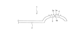
図1に示す電気コンタクト1は、DDRソケットコネクタ等の電気コネクタに用いられる電気コンタクトであって、当該電気コネクタの絶縁性ハウジング(図示せず)に固定される固定部(図示せず)から延びる弾性アーム部2を備えている。弾性アーム部2の先端には、図3に示すように、相手基板10の導電性を有する導体パターン(被接触物)に接触する接触部3が設けられている。接触部3は、図1及び図2(A)に示すように、弾性アーム部2の先端から上側が凸になるように湾曲して形成され、相手基板10の導体パターンとの接触面4も上側が凸の湾曲面となっている。一方、固定部の弾性アーム部2が延びる側と反対側には、コンタクト1を回路基板上に接続するための接続部(図示せず)が設けられている。この電気コンタクト1は、金属板に対し後に述べるドラッギング、スタンピング(打抜き加工)及びフォーミング(曲げ加工)することによって形成される。
Hereinafter, embodiments of the present invention will be described with reference to the drawings.
An electrical contact 1 shown in FIG. 1 is an electrical contact used for an electrical connector such as a DDR socket connector, and extends from a fixed portion (not shown) fixed to an insulating housing (not shown) of the electrical connector. An
そして、接触部3の接触面4には、図1及び図2(A)に示すように、接触面4から上方に突出して相手基板10の導体パターンとの接点を構成する複数対(本実施形態にあっては3対)の凸条5aが設けられている。相手基板10の導体パターンが、接触部3の接触面4に接触するといっても、実際には、図3に示すように、接点を構成する凸条5aの先端部に接触する。各対の凸条5a間には、図1及び図2(A)に示すように、接触面4から凹む略V字形の溝5bが形成されている。各溝5bは、ワイピング方向(図2(A)における矢印W方向)と直交する方向(図2(A)における紙面と直交する方向)に延びている。対をなす凸条5aは、溝5bの両側に当該溝5bに沿うように延びている。
As shown in FIGS. 1 and 2 (A), a plurality of pairs (this embodiment) projecting upward from the
ここで、これら各対の凸条5a及び溝5bは、ドラッギングによって形成される。即ち、これら各対の凸条5a及び溝5bは、ワイピング方向(図2(A)における矢印W方向)と直交する方向(図2(A)における紙面と直交する方向)に、断面方形状の治具等の機械的手段によって接触面4を引っ掻くことにより形成される。ドラッギングによって削られた板材の材料は、材料から剥離することなく、溝5bの両側に盛り上がり、効果的に凸条5aとして形成されるのに供される。このドラッギングは、金属板をスタンピングする前に行われる。
Here, each of these pairs of
そして、これら凸条5a及び溝5bの寸法としては、対をなす凸条5a間の距離dが100μm、凸条5aの高さhが35μm、溝5bの最深部における幅wが15μm、凸条5aの先端から溝5bの最深部までの深さDが70μm、互いに隣接する凸条5a間の距離Pが100μm、とすることが好ましい。
特に、凸条5aの先端から溝5bの最深部までの深さDを深くして電気コンタクト1の板厚に近づけることで、溝5bが深くなる。これにより、ワイピング時に掻き取られた異物が溝5b内に収容されるときにその異物の収容量を多くすることができ、クリーニング効果を一層上げることができる。
And, as the dimensions of these
In particular, the
また、図2(B)に示す各凸条5aの先端部の半径Rは、5〜15μmとする。この先端部の半径Rが5μm未満であると、半径Rが5μm未満の先端部を有する凸条5aをドラッギングによって作成することができない。また、当該半径Rが5μm未満であると、被接触物が凸条5aの先端部に接触した際に凸条5aの先端部が被接触物に突き刺さり、弾性アーム部2が塑性変形するおそれがある。一方、当該先端部の半径Rが15μmよりも大きいと、0.098N〜0.147N程度の低荷重すなわち低い接圧のときに高い集中応力(ハーツストレス)が得られず、相手基板10の導体パターン(被接触物)との接点における接触抵抗値を低くすることができず、かつ、当該接触抵抗値のばらつきが大きい電気コンタクトになってしまう。従って、各凸条5aの先端部の半径Rは、5〜15μmとする。
Moreover, the radius R of the front-end | tip part of each protruding item |
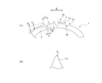
発明者らは、各凸条5aの先端部の半径Rを5〜15μmとすることの根拠について検証すべく、接点を構成する凸条5aにおける抵抗値と接点を構成する凸条5aの先端部の半径Rとの関係を調査するための試験を行った。
この試験に際しては、図5に示すように、リン青銅で構成される接触部3にドラッギングにより1対の凸条5aを形成したものを用いた。そして、凸条5aの先端部の半径Rにつき、5μmのサンプルを3つ(N1,N2,N3)、15μmのサンプルを3つ(N1、N2,N3)、25μmのサンプルを3つ(N1,N2,N3)、50μmのサンプルを3つ(N1,N2,N3)、200μmのサンプルを3つ(N1,N2,N3)用意した。
In order to verify the grounds for setting the radius R of the tip of each
In this test, as shown in FIG. 5, a
そして、それぞれのサンプルについて弾性アーム部2を固定し、金属板Mとして、銅板の接点部に金めっきを施したものを、凸条5aに対して、図5に示すように、接触させた。このときの凸条5aに対する金属板Mの荷重Fは、0.098Nとした。
このときの各サンプルにおける接点を構成する凸条5aと金属板Mとの間の抵抗値を測定した。この結果を、表1及び図6に示す。
And the
At this time, the resistance value between the

表1及び図6を参照すると、凸条5aの先端部の半径Rが5μmのサンプルN1、N2、N3の抵抗値は40、50、45mΩであり、同半径Rが15μmのサンプルN1、N2、N3の抵抗値は50、60、55mΩであった。従って、同半径Rが5μmのサンプルについて抵抗値の平均値が45mΩ、抵抗値最大値と最小値との差が10mΩで、金属板(被接触物)Mとの接点における接触抵抗値が低く、かつ、ばらつきの小さいものであることがわかった。また、同半径Rが15μmのサンプルについて抵抗値の平均値が55mΩ、抵抗値最大値と最小値との差が10mΩで、金属板Mとの接点における接触抵抗値が低く、かつ、ばらつきの小さいものであることがわかった。従って、この結果より、同半径Rが5μm〜15μmまでのものについては、金属板Mとの接点における接触抵抗値が低く、かつ、ばらつきが小さい安定領域であると言える。
Referring to Table 1 and FIG. 6, the resistance values of samples N1, N2, and N3 having a radius R of 5 μm at the tip of the
一方、凸条5aの先端部の半径Rが25μmのサンプルN1、N2、N3の抵抗値は210、325、140mΩであり、同半径Rが50μmのサンプルN1、N2、N3の抵抗値は435、500、325mΩであり、更に同半径Rが200μmのサンプルN1、N2、N3の抵抗値は625、750、450mΩであった。従って、同半径Rが25μmのサンプルについての抵抗値の平均値が225mΩ、抵抗値最大値と最小値との差が185mΩで、金属板Mとの接点における接触抵抗値が高く、かつ、ばらつきが大きいものであることがわかった。また、同半径Rが50μmのサンプルについて抵抗値の平均値が420mΩ、抵抗値最大値と最小値との差が175mΩで、金属板Mとの接点における接触抵抗値が高く、かつ、ばらつきが大きいものであることがわかった。更に、同半径Rが200μmのサンプルについて抵抗値の平均値が608mΩ、抵抗値最大値と最小値との差が300mΩで、金属板Mとの接点における接触抵抗値が高く、かつ、ばらつきが大きいものであることがわかった。従って、この結果より、同半径Rが15μmを超えるものについては、金属板Mとの接点における接触抵抗値が高く、かつ、ばらつきが大きい不安定領域であると言える。
On the other hand, the resistance values of the samples N1, N2, and N3 having a radius R of 25 μm at the tip of the
従って、発明者らは、被接触物との接点における接触抵抗値が低く、かつ、ばらつきが小さい安定領域を得るために、各凸条5aの先端部の半径Rを15μm以下としたのである。
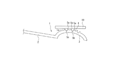
このように構成された電気コンタクト1に相手基板10の導体パターンが接触する様子を図3及び図4に示す。
図3に示すように、電気コンタクト1の3対ある凸条5aのうち中央の対をなす凸条5aに対し、相手基板10が平行な状態で接触する。すると、相手基板10の導体パターンは、3対ある凸条5aのうち中央の対をなす凸条5aに接触する。これにより、相手基板10の導体パターンと電気コンタクト1とが電気的に導通することになる。また、電気コンタクト1の当該凸条5aに対し、相手基板10が平行な状態からわずかな角度ずれた状態で接触した場合、相手基板10の導体パターンは、3対ある凸条5aのうち中央の対をなす凸条5aの一方に接触する。
Therefore, the inventors set the radius R of the tip portion of each
FIGS. 3 and 4 show a state in which the conductor pattern of the
As shown in FIG. 3, the
この際、凸条5aは図3及び図2(B)におけるW方向にワイピングする。すると、ワイピング時に掻き取られた異物が溝5b内に収容される。本実施形態にあっては、対の凸条5a間に、接触面4から凹む溝5bを設けたので、ワイピング時に掻き取られた異物を当該溝5b内に収容でき、クリーニング効果を上げることができる。そして、前述したように、凸条5aの先端から溝5bの最深部までの深さDを深くして電気コンタクト1の板厚に近づけることで、溝5bが深くなる。これにより、異物の収容量を多くすることができ、より一層クリーニング効果を上げることができる。
At this time, the
一方、図4に示すように、電気コンタクト1の3対ある凸条5aのうち中央の対をなす凸条5aに対し、相手基板10が平行な状態から大きく角度がずれた場合には、相手基板10の導体パターンは、3対ある凸条5aのうち中央の対をなす凸条5aに隣接した対をなす凸条5aの一方又は双方に接触する。これは、接触部3の接触面4が湾曲面を構成し、複数対(本実施形態の場合3対)の凸条が湾曲面に設けられていることから可能となる。この際に、相手基板10の導体パターンが接触する凸条5aは1つ又は2つであるから、相手基板10の導体パターンが0.098N〜0.147N程度の低荷重で接触しても高い集中応力を確保することができる。
On the other hand, as shown in FIG. 4, when the
これに対して、接触部3の接触面4が湾曲しない平らな平面状に形成され、その平面に複数対の凸条5aを設けた場合には、相手基板10の導体パターンが複数対の凸条5aの全てに接触することになる。なぜなら相手基板10の導体パターンが形成される面は、通常、湾曲していない平面で形成されるからである。この場合、相手基板10の導体パターンが0.098N〜0.147N程度の低荷重で接触すると、応力がすべての凸条5aに分散され、各凸条5aにおいて高い集中応力を確保することができない。
On the other hand, when the
従って、本実施形態にあっては、接触部3の接触面4を湾曲面で構成し、複数対の凸条5aを当該湾曲面に設けるようにしている。
以上、本発明の実施形態について説明してきたが、本発明はこれに限定されずに、種々の変更、改良を行うことができる。
例えば、電気コンタクト1は、接触部3の接触面4に少なくとも1対の凸条5aを設けたものであればよく、ハウジングへの固定部や回路基板への接続部がなくてもよい。
Therefore, in the present embodiment, the
As mentioned above, although embodiment of this invention has been described, this invention is not limited to this, A various change and improvement can be performed.
For example, the electrical contact 1 only needs to have at least one pair of
また、電気コンタクト1において、凸条5aは複数対設ける必要は必ずしもなく、少なくとも1対あればよい。例えば、凸条5aを、図5に示すように、1対設けてもあるいは図示はしないが2対、4対以上設けても良い。
更に、接触部3の接触面4は必ずしも湾曲面で構成されている必要はなく、また、対の凸条5a間に溝5bを必ずしも設けなくても良い。
また、被接触物として相手基板10の導体パターンが接触するようにしてあるが、導電性を有する被接触物であれば金属製のコンタクトや半導体バンプであってもよい。
In the electrical contact 1, it is not always necessary to provide a plurality of pairs of
Further, the
In addition, the conductor pattern of the
1 電気コンタクト
3 接触部
4 接触面
5a 凸条
5b 溝
10 相手基板
DESCRIPTION OF SYMBOLS 1
Claims (3)
前記接触部の前記被接触物との接触面に、該接触面から突出して前記被接触物との接点を構成する少なくとも1対の凸条を設け、該凸条の各々の先端部の半径が5〜15μmとなっていることを特徴とする電気コンタクト。 In an electrical contact having a contact portion that contacts a contacted object having conductivity,
The contact surface of the contact portion with the object to be contacted is provided with at least one pair of protrusions that protrude from the contact surface and constitute a contact point with the object to be contacted, and the radius of each tip of the protrusions is An electrical contact having a thickness of 5 to 15 μm.
Priority Applications (3)
| Application Number | Priority Date | Filing Date | Title |
|---|---|---|---|
| JP2010156594A JP2012018869A (en) | 2010-07-09 | 2010-07-09 | Electric contact |
| KR1020110066368A KR20120005959A (en) | 2010-07-09 | 2011-07-05 | Electrical contact |
| CN2011102008748A CN102340067A (en) | 2010-07-09 | 2011-07-07 | Electrical contact |
Applications Claiming Priority (1)
| Application Number | Priority Date | Filing Date | Title |
|---|---|---|---|
| JP2010156594A JP2012018869A (en) | 2010-07-09 | 2010-07-09 | Electric contact |
Publications (2)
| Publication Number | Publication Date |
|---|---|
| JP2012018869A true JP2012018869A (en) | 2012-01-26 |
| JP2012018869A5 JP2012018869A5 (en) | 2013-08-22 |
Family
ID=45515651
Family Applications (1)
| Application Number | Title | Priority Date | Filing Date |
|---|---|---|---|
| JP2010156594A Pending JP2012018869A (en) | 2010-07-09 | 2010-07-09 | Electric contact |
Country Status (3)
| Country | Link |
|---|---|
| JP (1) | JP2012018869A (en) |
| KR (1) | KR20120005959A (en) |
| CN (1) | CN102340067A (en) |
Cited By (3)
| Publication number | Priority date | Publication date | Assignee | Title |
|---|---|---|---|---|
| WO2014038617A1 (en) * | 2012-09-06 | 2014-03-13 | 矢崎総業株式会社 | Terminal |
| JP2019164930A (en) * | 2018-03-20 | 2019-09-26 | 古河電気工業株式会社 | Terminal |
| WO2021192759A1 (en) | 2020-03-27 | 2021-09-30 | 日本航空電子工業株式会社 | Contact member, connector, composition, and method for manufacturing contact member |
Families Citing this family (2)
| Publication number | Priority date | Publication date | Assignee | Title |
|---|---|---|---|---|
| CN105702358B (en) * | 2016-03-29 | 2018-07-27 | 江苏金坤科技有限公司 | Reduce contact resistance and the firm stiffening plate of bonding |
| DE102018216721A1 (en) * | 2018-09-28 | 2020-04-02 | Siemens Aktiengesellschaft | Contact arm and method for contacting a circuit breaker |
Citations (4)
| Publication number | Priority date | Publication date | Assignee | Title |
|---|---|---|---|---|
| JPH0536447A (en) * | 1991-07-30 | 1993-02-12 | Japan Aviation Electron Ind Ltd | Contact having contact part having precise stepped surface and manufacture of the same |
| JP2003229193A (en) * | 2002-02-05 | 2003-08-15 | Ricoh Co Ltd | Connector or socket |
| JP2005078865A (en) * | 2003-08-29 | 2005-03-24 | Tyco Electronics Amp Kk | Ic socket and contact used therefor |
| JP2006228669A (en) * | 2005-02-21 | 2006-08-31 | I-Pex Co Ltd | Connection terminal of electric connector |
Family Cites Families (2)
| Publication number | Priority date | Publication date | Assignee | Title |
|---|---|---|---|---|
| JPS58175220A (en) * | 1982-04-07 | 1983-10-14 | 株式会社東芝 | Electric contactor |
| CN201112733Y (en) * | 2007-09-07 | 2008-09-10 | 上海百川连接器有限公司 | Trifurcate connection contact sheet used for network plug |
-
2010
- 2010-07-09 JP JP2010156594A patent/JP2012018869A/en active Pending
-
2011
- 2011-07-05 KR KR1020110066368A patent/KR20120005959A/en not_active Application Discontinuation
- 2011-07-07 CN CN2011102008748A patent/CN102340067A/en active Pending
Patent Citations (4)
| Publication number | Priority date | Publication date | Assignee | Title |
|---|---|---|---|---|
| JPH0536447A (en) * | 1991-07-30 | 1993-02-12 | Japan Aviation Electron Ind Ltd | Contact having contact part having precise stepped surface and manufacture of the same |
| JP2003229193A (en) * | 2002-02-05 | 2003-08-15 | Ricoh Co Ltd | Connector or socket |
| JP2005078865A (en) * | 2003-08-29 | 2005-03-24 | Tyco Electronics Amp Kk | Ic socket and contact used therefor |
| JP2006228669A (en) * | 2005-02-21 | 2006-08-31 | I-Pex Co Ltd | Connection terminal of electric connector |
Cited By (4)
| Publication number | Priority date | Publication date | Assignee | Title |
|---|---|---|---|---|
| WO2014038617A1 (en) * | 2012-09-06 | 2014-03-13 | 矢崎総業株式会社 | Terminal |
| US9525229B2 (en) | 2012-09-06 | 2016-12-20 | Yazaki Corporation | Terminal |
| JP2019164930A (en) * | 2018-03-20 | 2019-09-26 | 古河電気工業株式会社 | Terminal |
| WO2021192759A1 (en) | 2020-03-27 | 2021-09-30 | 日本航空電子工業株式会社 | Contact member, connector, composition, and method for manufacturing contact member |
Also Published As
| Publication number | Publication date |
|---|---|
| CN102340067A (en) | 2012-02-01 |
| KR20120005959A (en) | 2012-01-17 |
Similar Documents
| Publication | Publication Date | Title |
|---|---|---|
| WO2017217042A1 (en) | Probe pin | |
| WO2017217041A1 (en) | Probe pin | |
| EP2590268A1 (en) | Female terminal fitting and production method therefor | |
| JP4532308B2 (en) | Electrical connector connection terminals | |
| US8647129B2 (en) | Housingless connector | |
| US11187722B2 (en) | Probe pin and electronic device using the same | |
| JP2012018869A (en) | Electric contact | |
| JP2009180549A (en) | Contact pin | |
| JP2021180196A (en) | Electric connector and electric connector assembly | |
| JP6583582B2 (en) | Probe pin | |
| JP2019191196A (en) | Probe pin | |
| EP2869404B1 (en) | Connector | |
| JP2018072157A (en) | Electric contactor and electric connection device including the same | |
| JP2005293989A (en) | Terminal for electrical connection | |
| JP6256129B2 (en) | Pressure contact terminal | |
| JP2019207245A (en) | Probe pin | |
| KR20160116185A (en) | Semiconductor test socket and manufacturing method thereof | |
| US20220018875A1 (en) | Contact pin and socket | |
| JP2020170008A (en) | Probe pin | |
| KR101819191B1 (en) | Contact probe | |
| JP2014099391A (en) | Terminal for electrical connection, and connector having the same | |
| KR101344935B1 (en) | contact for connector | |
| WO2009090907A1 (en) | Probe card and method for manufacturing the same | |
| WO2015136790A1 (en) | Pressure contact terminal | |
| JP2015216110A (en) | Contact connection structure |
Legal Events
| Date | Code | Title | Description |
|---|---|---|---|
| A521 | Written amendment |
Free format text: JAPANESE INTERMEDIATE CODE: A523 Effective date: 20130704 |
|
| A621 | Written request for application examination |
Free format text: JAPANESE INTERMEDIATE CODE: A621 Effective date: 20130704 |
|
| A977 | Report on retrieval |
Free format text: JAPANESE INTERMEDIATE CODE: A971007 Effective date: 20140227 |
|
| A131 | Notification of reasons for refusal |
Free format text: JAPANESE INTERMEDIATE CODE: A131 Effective date: 20140408 |
|
| A02 | Decision of refusal |
Free format text: JAPANESE INTERMEDIATE CODE: A02 Effective date: 20140819 |