JP2012015400A - Solid-state imaging device - Google Patents
Solid-state imaging device Download PDFInfo
- Publication number
- JP2012015400A JP2012015400A JP2010151973A JP2010151973A JP2012015400A JP 2012015400 A JP2012015400 A JP 2012015400A JP 2010151973 A JP2010151973 A JP 2010151973A JP 2010151973 A JP2010151973 A JP 2010151973A JP 2012015400 A JP2012015400 A JP 2012015400A
- Authority
- JP
- Japan
- Prior art keywords
- transistor
- pixel
- conductivity type
- well
- amplification
- Prior art date
- Legal status (The legal status is an assumption and is not a legal conclusion. Google has not performed a legal analysis and makes no representation as to the accuracy of the status listed.)
- Pending
Links
- 238000003384 imaging method Methods 0.000 title claims abstract description 27
- 230000003321 amplification Effects 0.000 claims abstract description 91
- 238000003199 nucleic acid amplification method Methods 0.000 claims abstract description 91
- 239000000758 substrate Substances 0.000 claims abstract description 62
- 238000006243 chemical reaction Methods 0.000 claims abstract description 42
- 239000004065 semiconductor Substances 0.000 claims description 22
- 239000011159 matrix material Substances 0.000 claims description 5
- 230000002093 peripheral effect Effects 0.000 abstract description 14
- 238000000926 separation method Methods 0.000 abstract description 7
- 238000010586 diagram Methods 0.000 description 13
- 230000008859 change Effects 0.000 description 4
- 230000000694 effects Effects 0.000 description 4
- 230000003071 parasitic effect Effects 0.000 description 3
- 229910021420 polycrystalline silicon Inorganic materials 0.000 description 3
- 229920005591 polysilicon Polymers 0.000 description 3
- 101100270422 Rattus norvegicus Arhgef7 gene Proteins 0.000 description 2
- 239000012535 impurity Substances 0.000 description 2
- 230000001629 suppression Effects 0.000 description 2
- 230000002411 adverse Effects 0.000 description 1
- 230000000052 comparative effect Effects 0.000 description 1
- 230000007423 decrease Effects 0.000 description 1
- 230000005669 field effect Effects 0.000 description 1
- 239000012212 insulator Substances 0.000 description 1
- 238000005468 ion implantation Methods 0.000 description 1
- 238000000034 method Methods 0.000 description 1
- 238000003825 pressing Methods 0.000 description 1
- 230000008569 process Effects 0.000 description 1
- 230000009467 reduction Effects 0.000 description 1
- 230000004044 response Effects 0.000 description 1
- 229920006395 saturated elastomer Polymers 0.000 description 1
- 230000035945 sensitivity Effects 0.000 description 1
Images


Classifications
-
- H—ELECTRICITY
- H01—ELECTRIC ELEMENTS
- H01L—SEMICONDUCTOR DEVICES NOT COVERED BY CLASS H10
- H01L27/00—Devices consisting of a plurality of semiconductor or other solid-state components formed in or on a common substrate
- H01L27/14—Devices consisting of a plurality of semiconductor or other solid-state components formed in or on a common substrate including semiconductor components sensitive to infrared radiation, light, electromagnetic radiation of shorter wavelength or corpuscular radiation and specially adapted either for the conversion of the energy of such radiation into electrical energy or for the control of electrical energy by such radiation
- H01L27/144—Devices controlled by radiation
- H01L27/146—Imager structures
- H01L27/14643—Photodiode arrays; MOS imagers
-
- H—ELECTRICITY
- H01—ELECTRIC ELEMENTS
- H01L—SEMICONDUCTOR DEVICES NOT COVERED BY CLASS H10
- H01L27/00—Devices consisting of a plurality of semiconductor or other solid-state components formed in or on a common substrate
- H01L27/14—Devices consisting of a plurality of semiconductor or other solid-state components formed in or on a common substrate including semiconductor components sensitive to infrared radiation, light, electromagnetic radiation of shorter wavelength or corpuscular radiation and specially adapted either for the conversion of the energy of such radiation into electrical energy or for the control of electrical energy by such radiation
- H01L27/144—Devices controlled by radiation
- H01L27/146—Imager structures
- H01L27/14601—Structural or functional details thereof
- H01L27/14609—Pixel-elements with integrated switching, control, storage or amplification elements
-
- H—ELECTRICITY
- H01—ELECTRIC ELEMENTS
- H01L—SEMICONDUCTOR DEVICES NOT COVERED BY CLASS H10
- H01L27/00—Devices consisting of a plurality of semiconductor or other solid-state components formed in or on a common substrate
- H01L27/14—Devices consisting of a plurality of semiconductor or other solid-state components formed in or on a common substrate including semiconductor components sensitive to infrared radiation, light, electromagnetic radiation of shorter wavelength or corpuscular radiation and specially adapted either for the conversion of the energy of such radiation into electrical energy or for the control of electrical energy by such radiation
- H01L27/144—Devices controlled by radiation
- H01L27/146—Imager structures
- H01L27/14601—Structural or functional details thereof
- H01L27/14632—Wafer-level processed structures
-
- H—ELECTRICITY
- H01—ELECTRIC ELEMENTS
- H01L—SEMICONDUCTOR DEVICES NOT COVERED BY CLASS H10
- H01L27/00—Devices consisting of a plurality of semiconductor or other solid-state components formed in or on a common substrate
- H01L27/14—Devices consisting of a plurality of semiconductor or other solid-state components formed in or on a common substrate including semiconductor components sensitive to infrared radiation, light, electromagnetic radiation of shorter wavelength or corpuscular radiation and specially adapted either for the conversion of the energy of such radiation into electrical energy or for the control of electrical energy by such radiation
- H01L27/144—Devices controlled by radiation
- H01L27/146—Imager structures
- H01L27/14601—Structural or functional details thereof
- H01L27/14634—Assemblies, i.e. Hybrid structures
-
- H—ELECTRICITY
- H01—ELECTRIC ELEMENTS
- H01L—SEMICONDUCTOR DEVICES NOT COVERED BY CLASS H10
- H01L27/00—Devices consisting of a plurality of semiconductor or other solid-state components formed in or on a common substrate
- H01L27/14—Devices consisting of a plurality of semiconductor or other solid-state components formed in or on a common substrate including semiconductor components sensitive to infrared radiation, light, electromagnetic radiation of shorter wavelength or corpuscular radiation and specially adapted either for the conversion of the energy of such radiation into electrical energy or for the control of electrical energy by such radiation
- H01L27/144—Devices controlled by radiation
- H01L27/146—Imager structures
- H01L27/14601—Structural or functional details thereof
- H01L27/1464—Back illuminated imager structures
-
- H—ELECTRICITY
- H01—ELECTRIC ELEMENTS
- H01L—SEMICONDUCTOR DEVICES NOT COVERED BY CLASS H10
- H01L27/00—Devices consisting of a plurality of semiconductor or other solid-state components formed in or on a common substrate
- H01L27/14—Devices consisting of a plurality of semiconductor or other solid-state components formed in or on a common substrate including semiconductor components sensitive to infrared radiation, light, electromagnetic radiation of shorter wavelength or corpuscular radiation and specially adapted either for the conversion of the energy of such radiation into electrical energy or for the control of electrical energy by such radiation
- H01L27/144—Devices controlled by radiation
- H01L27/146—Imager structures
- H01L27/14601—Structural or functional details thereof
- H01L27/14636—Interconnect structures
Abstract
Description
本発明は固体撮像装置に関する。 The present invention relates to a solid-state imaging device.
固体撮像装置において、光電変換部と、周辺回路部もしくは画素回路の一部とを別基板に分けて形成し、それらを電気的に接続する構成が知られている。 In a solid-state imaging device, a configuration in which a photoelectric conversion unit and a peripheral circuit unit or a part of a pixel circuit are formed separately on different substrates and are electrically connected to each other is known.
特許文献1には、第1の基板に受光画素および貫通配線とが配され、第2の基板に読み出し回路が配された構成が開示されている。読み出し回路は、貫通配線を介して電気信号を読み出して画像信号として出力する。この固体撮像装置は、第1の基板の反対面と、第2の基板の読み出し回路とが対向する向きに配置され、貫通配線と読み出し回路との端子間が電気的に接合された構成となっている。
また特許文献2には一の基板に光電変換部及び画素回路とをモノリシックに配した構成において、光電変換部を構成するウエルを画素毎に分離する構成が開示されている。 Patent Document 2 discloses a configuration in which a photoelectric conversion unit and a pixel circuit are monolithically arranged on a single substrate, and a well constituting the photoelectric conversion unit is separated for each pixel.
更に特許文献3には、一の基板に光電変換部及び画素回路とをモノリシックに配した構成において、アンプ用トランジスタのウエルを画素に含まれる他のトランジスタのウエルと電気的に分離した構成が開示されている。 Further, Patent Document 3 discloses a configuration in which a well of an amplifier transistor is electrically separated from a well of another transistor included in a pixel in a configuration in which a photoelectric conversion unit and a pixel circuit are monolithically arranged on one substrate. Has been.
特許文献1〜3においては、光電変換部と、周辺回路部もしくは画素回路の一部とを別基板に分けて電気的に接続する構成において、好適なウエルの分離構造に関しては検討が不充分であった。
In
ウエルを分離している特許文献2においては、飽和した画素から漏れ出した電荷による影響を考慮して光電変換部を構成するウエルを画素毎に分離している。そのため、基板を分けた構成において光電変換部が配されない基板のウエル分離に関して何等述べられていない。 In Patent Document 2 in which wells are separated, the wells constituting the photoelectric conversion unit are separated for each pixel in consideration of the influence of charges leaking from saturated pixels. For this reason, nothing is described regarding well separation of a substrate in which a photoelectric conversion unit is not arranged in a configuration in which the substrate is divided.
また特許文献3においては、画素を構成するアンプ用トランジスタの基板バイアス効果によるしきい値の変動を抑えることを目的としてアンプ用トランジスタのウエルを、画素の他のトランジスタのウエルと分離している。しかしながら他の画素に含まれるアンプ用トランジスタどうしのウエルに関しては何等述べられていない。 In Patent Document 3, the well of the transistor for amplifier is separated from the well of other transistors in the pixel for the purpose of suppressing the fluctuation of the threshold due to the substrate bias effect of the amplifier transistor constituting the pixel. However, nothing is said about wells between amplifier transistors included in other pixels.
また特許文献2、3に共通していえるのは、一の基板に光電変換部と画素回路とがモノリシックに配された構成であるため、ウエルを分離するために余分なスペースが必要となり、光電変換部の受光面積を圧迫するという課題があった。 In addition, what can be said in common with Patent Documents 2 and 3 is a configuration in which the photoelectric conversion unit and the pixel circuit are monolithically arranged on one substrate, so that an extra space is required to separate the wells, and the photoelectric conversion unit and the pixel circuit are separated. There was a problem of pressing the light receiving area of the converter.
本発明は上記課題に鑑み、光電変換部と、周辺回路部もしくは画素回路の一部とを別基板に分けて電気的に接続する構成における好適なウエルの分離構造を提供することを目的とする。 In view of the above problems, an object of the present invention is to provide a preferable well separation structure in a configuration in which a photoelectric conversion portion and a peripheral circuit portion or a part of a pixel circuit are electrically connected to different substrates. .
本発明は、光電変換部と、該光電変換部で生じた信号を増幅する増幅トランジスタとを含む画素を複数有し、複数の光電変換部が配された第1の基板と、複数の増幅トランジスタが配された第2の基板とを有する固体撮像装置であって、前記増幅トランジスタのソース領域及びドレイン領域が配される第1導電型のウエルは、少なくとも一方向に隣接する増幅トランジスタのソース領域及びドレイン領域が配される第1導電型のウエルと分離されていることを特徴とする。 The present invention includes a plurality of pixels including a photoelectric conversion unit and an amplification transistor that amplifies a signal generated in the photoelectric conversion unit, a first substrate on which the plurality of photoelectric conversion units are arranged, and a plurality of amplification transistors A first substrate having a source region and a drain region of the amplification transistor, wherein the well of the first conductivity type in which the source region and the drain region of the amplification transistor are disposed is adjacent to at least one direction of the source region of the amplification transistor And a well of the first conductivity type in which the drain region is disposed.
本発明によれば、光電変換部と、周辺回路部もしくは画素回路の一部とを別基板に分けて電気的に接続する構成における好適なウエルの分離構造を提供することが可能となる。 According to the present invention, it is possible to provide a suitable well separation structure in a configuration in which a photoelectric conversion unit and a peripheral circuit unit or a part of a pixel circuit are electrically connected to different substrates.
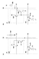
図1に本発明に適用可能な固体撮像装置の1画素の等価回路の一例を示す。ここでは1画素のみを示すが実際には画素を複数有して画素配列が構成される。 FIG. 1 shows an example of an equivalent circuit of one pixel of a solid-state imaging device applicable to the present invention. Although only one pixel is shown here, a pixel array is actually configured with a plurality of pixels.
101は光電変換部である。光電変換により正孔と電子を生じる。例えばフォトダイオードが用いられる。
102は転送部である。光電変換部の電荷を転送する。例えばMOSトランジスタ(転送トランジスタ)が用いられる。
103はFDである。電位がフローティング状態で転送部により光電変換部の電荷が転送される。
104は画素リセット部である。少なくともFDの電位を基準電位に設定する。言い換えると、増幅トランジスタの入力ノードの電圧をリセットしているともいえる。または転送部と同時にオン状態とすることにより光電変換部の電位を基準電位に設定する。画素リセット部としては、例えばMOSトランジスタ(リセットトランジスタ)が用いられる。 Reference numeral 104 denotes a pixel reset unit. At least the potential of FD is set to the reference potential. In other words, it can be said that the voltage at the input node of the amplification transistor is reset. Alternatively, the potential of the photoelectric conversion unit is set to the reference potential by being turned on simultaneously with the transfer unit. For example, a MOS transistor (reset transistor) is used as the pixel reset unit.
105は画素増幅部である。光電変換部で生じた電荷対のうち一方の電荷に基づく信号を増幅して出力する。例えばMOSトランジスタが用いられ、この場合には画素増幅部のMOSトランジスタ(増幅トランジスタ)のゲートとFDとが電気的に接続された構成となる。
106は転送トランジスタの動作を制御するための転送制御線である。107はリセットトランジスタの動作を制御するためのリセット制御線である。これら制御線には不図示の垂直走査回路からの駆動パルスが供給される。
108は垂直出力線である。垂直出力線108には、画素列に含まれる複数の画素増幅部で増幅された信号が順次出力される。
109は電流源である。増幅部へバイアス電流を供給するためのものである。本回路構成においては増幅MOSトランジスタをソースフォロワ動作させるためのバイアス電流を供給するものである。 Reference numeral 109 denotes a current source. This is for supplying a bias current to the amplifying unit. In this circuit configuration, a bias current for operating the amplification MOS transistor as a source follower is supplied.
V1は図1(a)において増幅トランジスタ及びリセットトランジスタのドレインに供給される電圧である。ここでは共通電圧で記載しているが別電源とすることも可能である。V2は図1(a)において電流源109aに供給される電圧である。 V1 is a voltage supplied to the drains of the amplification transistor and the reset transistor in FIG. Although the common voltage is described here, a separate power source may be used. V2 is a voltage supplied to the current source 109a in FIG.
V3は図1(b)においてリセットトランジスタのドレインに供給される電圧である。V4は図1(b)において増幅トランジスタのドレインに供給される電圧である。V5は図1(b)において電流源109bに供給される電圧である。 V3 is a voltage supplied to the drain of the reset transistor in FIG. V4 is a voltage supplied to the drain of the amplification transistor in FIG. V5 is a voltage supplied to the current source 109b in FIG.
画素を構成する要素のうち、pixAは第1の基板に配される部分を示し、pixBは第2の基板に配される部分を示している。pixA、pixBにより画素pixが構成される。 Of the elements constituting the pixel, pixA indicates a portion disposed on the first substrate, and pixB indicates a portion disposed on the second substrate. A pixel pix is configured by pixA and pixB.
ここで図1(a)と(b)との違いについて説明する。異なる部材にはそれぞれ添字a、bを振って区別している。具体的には、増幅トランジスタ及びリセットトランジスタの導電型が異なり、図1(a)においてはNMOSトランジスタが用いられ、図1(b)においてはPMOSトランジスタが用いられる。これに対応してそれぞれのトランジスタ、電流源に供給される電圧が異なっている。 Here, the difference between FIGS. 1A and 1B will be described. Different members are distinguished from each other by adding subscripts a and b. Specifically, the conductivity types of the amplification transistor and the reset transistor are different. In FIG. 1A, an NMOS transistor is used, and in FIG. 1B, a PMOS transistor is used. Correspondingly, the voltages supplied to the respective transistors and current sources are different.
図1(a)において、V1は例えば5V、3.3Vなどの電源電圧である。V2はV1よりも低い電圧であり、例えば接地電位である。これに対して図1(b)のV3、V4は、接地電位などの相対的に低い電位であり、V5は3.3V、1.8VなどのV3に比べて高い電圧である。 In FIG. 1A, V1 is a power supply voltage such as 5V, 3.3V, for example. V2 is a voltage lower than V1, and is a ground potential, for example. On the other hand, V3 and V4 in FIG. 1B are relatively low potentials such as a ground potential, and V5 is a higher voltage than V3 such as 3.3V and 1.8V.
図1(b)は増幅トランジスタがPMOSトランジスタである。光電変換部は信号電荷として電子を用いる構成となっており、入射光量が大きい場合に、PMOSトランジスタのゲート電位は下がる。これに応じてPMOSトランジスタのソース電位は暗い場合に比べて上昇する方向である。つまり、リセット時に比べて信号振幅が大きい時の垂直出力線の駆動を駆動力が高い状態で行なうことが可能になる。したがって図1(a)の構成に比べて読み出し速度という観点で有利である。従来であれば、このような構成を同一基板に配していたため、画素内でウエルを分ける等、構造として複雑となってしまっていた。これに対して本発明のように、別基板に分けて構成することにより、このような弊害を抑制することが可能となる。更に動作電圧範囲も図1(b)の方を狭くすることが可能となり、低電源電圧化という観点で有利である。 In FIG. 1B, the amplification transistor is a PMOS transistor. The photoelectric conversion unit is configured to use electrons as signal charges, and the gate potential of the PMOS transistor decreases when the amount of incident light is large. In response to this, the source potential of the PMOS transistor tends to rise as compared to when it is dark. That is, it becomes possible to drive the vertical output line when the signal amplitude is larger than that at the time of resetting with a high driving force. Therefore, it is advantageous in terms of reading speed as compared with the configuration of FIG. Conventionally, since such a configuration is arranged on the same substrate, the structure is complicated, such as dividing wells in pixels. On the other hand, it is possible to suppress such an adverse effect by dividing the circuit board into separate substrates as in the present invention. Further, the operating voltage range can be made narrower in FIG. 1B, which is advantageous from the viewpoint of reducing the power supply voltage.
この本質は、増幅トランジスタがPMOSトランジスタである点ではなく、信号電荷と逆極性のトランジスタを用いることである。つまり、信号電荷が電子の場合には増幅トランジスタ及びリセットトランジスタにPMOSトランジスタ、信号電荷がホールの場合にはNMOSトランジスタを用いる点である。転送トランジスタの導電型で言えば、転送トランジスタが第1導電型のMOSトランジスタであり、増幅トランジスタ及びリセットトランジスタが第1導電型と逆導電型の第2導電型のトランジスタとなる。 The essence is not that the amplification transistor is a PMOS transistor but a transistor having a polarity opposite to that of the signal charge. That is, when the signal charge is an electron, a PMOS transistor is used as the amplification transistor and the reset transistor, and when the signal charge is a hole, an NMOS transistor is used. In terms of the conductivity type of the transfer transistor, the transfer transistor is a first conductivity type MOS transistor, and the amplification transistor and the reset transistor are second conductivity type transistors opposite to the first conductivity type.
以上、画素の構成に関して説明したがこれら構成に限られるものではない。例えば増幅トランジスタとして接合型電界効果型トランジスタ(JFET)を用いることもできる。また光電変換部としてホールを信号電荷として用いる構成としてもよい。この場合には転送トランジスタをPMOSトランジスタとする。また複数の光電変換部で増幅トランジスタ、リセットトランジスタを共有する構成としても良い。また、別途増幅トランジスタと直列に選択トランジスタを用いる構成としてもよい。また複数の基板への画素の構成を振り分ける例としては上記の構成に限られない。上記構成以外にも、リセットトランジスタ、増幅トランジスタを第1の基板に配しても良い。更に画素に、増幅トランジスタ、リセットトランジスタを設けずに、転送トランジスタにより光電変換部の電荷を直接垂直出力線へ出力する構成としてもよい。 Although the pixel configurations have been described above, the present invention is not limited to these configurations. For example, a junction field effect transistor (JFET) can be used as the amplification transistor. Alternatively, a hole may be used as the signal charge as the photoelectric conversion unit. In this case, the transfer transistor is a PMOS transistor. A plurality of photoelectric conversion units may share an amplification transistor and a reset transistor. Alternatively, a selection transistor may be separately used in series with the amplification transistor. Further, an example of distributing pixel configurations to a plurality of substrates is not limited to the above configuration. In addition to the above structure, a reset transistor and an amplification transistor may be provided on the first substrate. Further, the pixel may not be provided with an amplification transistor and a reset transistor, and the charge of the photoelectric conversion unit may be directly output to the vertical output line by the transfer transistor.
図2に、本発明の固体撮像装置に共通に適用可能な第1の基板及び第2の基板の電気的接続部を含めた断面の概念図の一例を示す。 FIG. 2 shows an example of a conceptual diagram of a cross section including an electrical connection portion of a first substrate and a second substrate that can be commonly applied to the solid-state imaging device of the present invention.
201は第1の基板である。202は第2の基板である。203aは第1の基板に配された画素領域である。203bは第2の基板に配された画素領域である。204aは第1の基板に配された第1の周辺領域である。第1の周辺領域204aは画素領域203a外に配される領域である。204bは第2の基板に配される第2の周辺領域である。第2の周辺領域204bは画素領域203b外に配される領域であり、画素領域から共通出力線を介して出力された信号の処理もしくは、画素領域からの信号出力を制御する回路が配される。
105は光電変換部である。206はFDである。207は増幅トランジスタである。そのゲートがFDと電気的に接続されている。ここでは画素回路として増幅トランジスタのみを示しているが、他に上述したリセットトランジスタなどが設けられる。
208は第2の周辺領域に配される読み出し回路の一部を構成するMOSトランジスタである。読み出し回路の一例として、複数の画素列ごとに読み出された信号を並列に処理する並列処理回路が挙げられる。このような並列処理回路しては列増幅器、列ADなどがある。209は第2の周辺回路に配される並列処理回路以外の回路を構成するMOSトランジスタである。
110は並列処理回路を構成するMOSトランジスタ209に直流電圧を供給する直流電圧供給配線を構成する第1の導電パターンである。第1の導電パターン110は、紙面奥行き方向に延在して、各並列処理回路のMOSトランジスタに共通に直流電圧を供給する。第1の導電パターンは画素領域外に配される。
211は第1の基板に配された第2の導電パターンである。第2の導電パターンは画素領域外に配される。
112は第1の導電パターン110と第2の導電パターン211とを電気的に接続する電気的接続部である。例えば、電気的接続部112は第1の基板に配された最上配線層と第2の基板に配された最上配線層により導電パターンを形成し、これらを電気的に接続することにより構成することができる。
第2の導電パターン211は第1の基板の第1の周辺領域に配される。第1の周辺領域は第2の基板に配される第2の周辺領域に比べ配置される回路素子が少ない、もしくは回路素子自体が存在しない。したがってレイアウトの自由度は比較的高いため、第2の導電パターンの面積を第1の導電パターン面積よりも大きくすることにより、第2の基板の配線レイアウトの自由度を維持しつつ、抵抗値を低下させることが可能となり好ましい。
The second
113はFD206と増幅トランジスタ207のゲートとを電気的に接続する電気的接続部である。第2の電気的接続部は第1の基板の最上配線層と第2の基板の最上配線層とにより導電パターンを形成し、これらを電気的に接続することにより構成することができる。
214は少なくとも1画素の増幅トランジスタ207のソース領域、ドレイン領域が配される第1導電型のウエルである。増幅トランジスタ207がNMOSトランジスタの場合にはウエルの導電型はP型であり、増幅トランジスタ207がPMOSトランジスタの場合にはウエルの導電型はN型である。つまり、ウエルはソース領域、ドレイン領域と反対導電型の半導体領域で構成される。
各ウエル114は少なくとも一方向に隣接するウエルと電気的に分離されている。つまり1つ目の実施形態としては、1つのウエルに1画素列に含まれる複数の増幅トランジスタのソース領域、ドレイン領域が配される構成である。この場合には隣接する画素列の増幅トランジスタのソース領域、ドレイン領域が配されるウエルどうしが分離されている。2つ目の実施形態としては、1つのウエルに1画素行に含まれる複数の増幅トランジスタのソース領域、ドレイン領域が配される構成である。この場合には隣接する画素行の増幅トランジスタのソース領域、ドレイン領域が配されるウエルどうしが分離されている。3つ目の実施形態としては1つのウエルに1画素の増幅トランジスタのソース領域、ドレイン領域が配される構成である。この場合には垂直方向及び水平方向に隣接する画素の増幅トランジスタのソース領域及びドレイン領域が配されるウエルと分離されている。 Each well 114 is electrically isolated from adjacent wells in at least one direction. That is, in the first embodiment, the source and drain regions of a plurality of amplification transistors included in one pixel column are arranged in one well. In this case, the wells in which the source regions and drain regions of the amplification transistors in the adjacent pixel columns are arranged are separated. In the second embodiment, a source region and a drain region of a plurality of amplification transistors included in one pixel row are arranged in one well. In this case, the wells in which the source regions and drain regions of the amplification transistors in adjacent pixel rows are arranged are separated from each other. In the third embodiment, a source region and a drain region of an amplification transistor of one pixel are arranged in one well. In this case, it is separated from the well in which the source region and the drain region of the amplification transistor of the pixel adjacent in the vertical direction and the horizontal direction are arranged.
代表的には上記3実施形態となるが、画素列ごと、画素行ごとにウエルが分離される場合には、更に、1画素行、1画素列内でウエルが分離されていてもよい。 Typically, the third embodiment is described. However, when the well is separated for each pixel column and each pixel row, the well may be further separated in one pixel row and one pixel column.
ここで分離されているとは、隣接するウエル214間に、該ウエルとは反対導電型の半導体領域が配されていることをいう。更に反対導電型の半導体領域に加えて絶縁体が配されていてもよい。215は第2導電型の半導体領域である。ウエル214とは反対導電型の半導体領域である。第2導電型の半導体領域215は隣接するウエル214間に配されて、各ウエルどうしを電気的に分離している。第2導電型の半導体領域215としては半導体基板そのもの、エピ層、もしくはイオン注入で形成された半導体領域を用いることができる。
Here, “isolated” means that a semiconductor region having a conductivity type opposite to the well 214 is disposed between
本発明は光電変換部が配されていない第2の基板において所定の単位で画素領域に配されるウエルを分離する。このため、従来1基板に光電変換部と画素回路とをモノリシックに配した場合に比べてウエル分離に伴なう光電変換部の受光面積低減を抑制することが可能となる。 The present invention separates wells arranged in a pixel region in a predetermined unit on a second substrate on which no photoelectric conversion unit is arranged. For this reason, it is possible to suppress a reduction in the light receiving area of the photoelectric conversion unit due to the well separation compared to the case where the photoelectric conversion unit and the pixel circuit are monolithically arranged on one substrate.
更に各実施例においては下記効果のいずれか1つを得ることが可能となる。 Furthermore, in each embodiment, any one of the following effects can be obtained.
第1点目は増幅トランジスタのゲインの向上である。第2点目はウエル214経由のクロストークの抑制である。第3点目はFD容量の増加の抑制である。
The first point is to improve the gain of the amplification transistor. The second point is suppression of crosstalk via the
以下具体的に実施例を挙げて本発明を詳細に説明する。 Hereinafter, the present invention will be described in detail with specific examples.
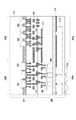
(実施例1)
本実施例はウエルを各画素毎に分離することを特徴とする。図3に第2の基板に配された画素回路部分の上面概念図を示す。本実施例においては画素回路を構成する部材のうち、第2の基板に増幅トランジスタ、リセットトランジスタ、画素を選択する選択トランジスタが配されている。
Example 1
This embodiment is characterized in that the well is separated for each pixel. FIG. 3 is a conceptual top view of the pixel circuit portion arranged on the second substrate. In this embodiment, among the members constituting the pixel circuit, an amplification transistor, a reset transistor, and a selection transistor for selecting a pixel are arranged on the second substrate.
301は第2の基板の画素領域を示している。画素を構成する上記部材が所定の繰り返しピッチで配されている。格子状に区画しているのは第2の基板において1画素が占有する領域を概念的に示しているものである。各画素が行列状に配されている。
302は第1導電型のウエルである。ここではP型とする。ウエル302は画素毎に分離されている。各ウエルには1画素回路を構成する増幅トランジスタ、リセットトランジスタ、選択トランジスタのソース領域、ドレイン領域が配されている。ソース領域、ドレイン領域はウエルと反対導電型である第2導電型の半導体領域により構成される。
303は第2導電型の半導体領域である。ここではN型とする。少なくとも各ウエル302間に配され、各ウエルを隣接するウエルと分離する。更に各ウエル302の下部に配されていてもよい。
304は画素回路を構成するリセットトランジスタ、選択トランジスタのゲートに駆動パルスを供給する制御線である。ここでは1本で示されているが、実際には各画素行に対してリセットトランジスタ用、選択トランジスタ用の計2本が設けられている。添え字は行番号を示している。
305は各画素行からの信号が並列に読み出される垂直信号線である。垂直信号線305は各画素列ごとに設けられている。添え字は列番号を示している。
図4に本実施例の固体撮像装置の1画素の等価回路図の一例を示す。 FIG. 4 shows an example of an equivalent circuit diagram of one pixel of the solid-state imaging device of the present embodiment.
401は光電変換部、402は転送部を構成する転送トランジスタ、403はFD、404は画素リセット部を構成するリセットトランジスタである。405は画素増幅部を構成する増幅トランジスタである。電流源と共にソースフォロワ回路を構成する。406は画素選択部を構成する選択トランジスタである。図1の構成と比較すると選択トランジスタを有している点が異なる。
401 is a photoelectric conversion unit, 402 is a transfer transistor that constitutes a transfer unit, 403 is an FD, and 404 is a reset transistor that constitutes a pixel reset unit.
光電変換部401、転送トランジスタ402、FD403が第1の基板に配され、リセットトランジスタ404、増幅トランジスタ405、選択トランジスタ406が第2の基板に配される。リセットトランジスタ404、増幅トランジスタ405、選択トランジスタ406はそれぞれN型のMOSトランジスタで構成される。
The
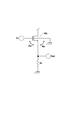
図5に第2の基板の上面概念図を示す。図3、4と同様の機能を有する部分には同様の符号を付し詳細な説明は省略する。 FIG. 5 is a conceptual top view of the second substrate. Portions having functions similar to those in FIGS. 3 and 4 are denoted by the same reference numerals, and detailed description thereof is omitted.
501は第1の基板との電気的接続部である。502は増幅トランジスタのゲート電極を構成するポリシリコンである。電気的接続部501を介して第1の基板に配されたFDと電気的に接続される。503は増幅トランジスタのソース領域である。504は増幅トランジスタのドレイン領域である。またドレイン領域504は選択トランジスタのソース領域を兼ねている。505は選択トランジスタのゲート電極を構成するポリシリコンである。506は選択トランジスタのソース領域である。507はリセットトランジスタのソース領域である。508はリセットトランジスタのゲート電極を構成するポリシリコンである。509はリセットトランジスタのドレイン領域である。
510はウエル302と同導電型の半導体領域である。ウエル302よりも不純物濃度が高い。ウエルに所定の電圧を供給する機能を有するため、以下ウエルコンタクト領域と呼ぶ。
511はリセットトランジスタに駆動パルスを供給するリセット制御線である。512はリセットトランジスタのドレインにリセット電圧を供給するリセット電源線である。513は選択トランジスタのゲートに駆動パルスを供給するための選択制御線である。514は増幅トランジスタのドレインにドレイン電圧を供給するための電源線である。515は垂直信号線である。
ここで、増幅トランジスタはソースフォロワ動作をする。光電変換部401で発生した電荷が転送トランジスタ402を介して増幅トランジスタのゲートに供給される。供給された電荷量に基づいて増幅トランジスタのゲート電圧が変化する。増幅トランジスタのゲート電圧の変化に基づいて増幅トランジスタのソース電圧が変化する。本実施例においてはウエル302がウエルコンタクト領域510を介して増幅トランジスタのソース504と電気的に接続されている。したがってウエル302の電位は画素ごとに増幅トランジスタのソースの電圧変化と同様に変化する。このような構成によればソースフォロワ回路のゲインを1に近づけることが可能となり、ソースフォロワ回路の電圧ゲインを向上させることが可能となる。これをより詳細に説明する。
Here, the amplification transistor performs a source follower operation. The charge generated in the
図6に比較例として増幅トランジスタのウエルが交流的に接地された場合を示す。例えばGNDである。ソースフォロワ回路のゲインは、増幅トランジスタのゲート・ソース間電圧をVgs、ソースとバックゲート間の電圧をVbs、負荷抵抗の抵抗値をRsとすると、以下の式で表される。
Av=ΔVin/ΔVout
=gm×Rs/(1+(gm+gmbs)×Rs) (数式1)
ここでAvはソースフォロワ回路の電圧ゲイン、gm=ΔIds/ΔVgs、gmbs=ΔIds/ΔVbsである。
FIG. 6 shows a case where the well of the amplification transistor is grounded in an alternating manner as a comparative example. For example, GND. The gain of the source follower circuit is expressed by the following equation, where Vgs is the gate-source voltage of the amplification transistor, Vbs is the voltage between the source and the back gate, and Rs is the resistance value of the load resistance.
Av = ΔVin / ΔVout
= Gm * Rs / (1+ (gm + gmbs) * Rs) (Formula 1)
Here, Av is a voltage gain of the source follower circuit, gm = ΔIds / ΔVgs, and gmbs = ΔIds / ΔVbs.
負荷抵抗の抵抗値Rs=∞とする。そうすると数式1は以下のように変形できる。
Av=gm/(gm+gmbs) (数式2)
数式2の値は通常0.8〜0.9の範囲である。ここで増幅トランジスタのソースをウエルと電気的に接続する、つまり増幅トランジスタのソースをバックゲートと接続することによりgmbs=0となる。このため、このときの電圧ゲインは1.0となる。したがって通常のようにバックゲートを交流的に接地する場合に比べて電圧ゲインを高くすることが可能となる。
The resistance value Rs of the load resistance is set to ∞. Then,
Av = gm / (gm + gmbs) (Formula 2)
The value of Equation 2 is usually in the range of 0.8 to 0.9. Here, gmbs = 0 is established by electrically connecting the source of the amplification transistor to the well, that is, connecting the source of the amplification transistor to the back gate. For this reason, the voltage gain at this time is 1.0. Therefore, the voltage gain can be increased as compared with the case where the back gate is grounded in an alternating manner as usual.
また更にリセットトランジスタを増幅トランジスタのソースと電気的に接続されたウエルに配すればFD容量も低減することが可能となる。これを説明するためにFDに生じる寄生容量の一部を図示したものを図7に示す。図7は、図4のリセットトランジスタと増幅トランジスタを抜き出したものである。701はFDとリセットトランジスタのバックゲートとの間に生じる寄生容量である。増幅トランジスタのウエルとソースとが電気的に接続された場合、増幅トランジスタのゲート・ソース間電圧がFD電位によらずほぼ一定となる。したがって寄生容量701がFD容量に寄与しない。これは増幅トランジスタのソースと同様の電圧変化をするためである。したがって、リセットトランジスタを増幅トランジスタと同じウエルに配することにより、FD容量を低減することが可能となる。これによって感度を向上させることが可能となる。
Further, if the reset transistor is arranged in a well electrically connected to the source of the amplification transistor, the FD capacitance can be reduced. In order to explain this, FIG. 7 shows a part of the parasitic capacitance generated in the FD. FIG. 7 shows the reset transistor and the amplification transistor extracted from FIG.
また本実施例においては垂直出力線と増幅トランジスタのソースとの間に選択トランジスタを配している。このような構成によれば、選択トランジスタを非導通とすることにより垂直出力線の電位変化のウエルへの影響を低減することが可能となり更に好ましい。 In this embodiment, a selection transistor is arranged between the vertical output line and the source of the amplification transistor. According to such a configuration, it is more preferable because the influence of the potential change of the vertical output line on the well can be reduced by making the selection transistor non-conductive.
以上述べたように本実施例によれば、光電変換部が配されない第2の基板に配された画素回路を構成するトランジスタのウエルを画素毎に分離した。このような構成によって、光電変換部の受光面積を低減させることなくウエルを分離することが可能となる。 As described above, according to the present embodiment, the wells of the transistors constituting the pixel circuit disposed on the second substrate where the photoelectric conversion unit is not disposed are separated for each pixel. With such a configuration, it is possible to separate the wells without reducing the light receiving area of the photoelectric conversion unit.
更に、増幅トランジスタのソースと該増幅トランジスタが配されるウエルとを電気的に接続することにより増幅トランジスタの電圧ゲインを向上させることが可能となる。また、リセットトランジスタを増幅トランジスタと同じウエルに配することにより、FD容量を低減させることが可能となる。更に、選択トランジスタを配して、垂直出力線と増幅トランジスタのソースとを電気的に分離させることにより、垂直出力線の電位変化のウエルへの影響を低減させることが可能となる。 Furthermore, the voltage gain of the amplification transistor can be improved by electrically connecting the source of the amplification transistor and the well in which the amplification transistor is disposed. Further, the FD capacitance can be reduced by arranging the reset transistor in the same well as the amplification transistor. Furthermore, by arranging a selection transistor to electrically isolate the vertical output line and the source of the amplification transistor, it is possible to reduce the influence of the potential change of the vertical output line on the well.
(実施例2)
本実施例の実施例1との違いは画素列間でウエルが分離されている点である。第2の基板に配置されるトランジスタで言えば、増幅トランジスタの列間でウエルが分離されているとも言える。
(Example 2)
The difference between the present embodiment and the first embodiment is that the wells are separated between the pixel columns. In terms of transistors arranged on the second substrate, it can be said that wells are separated between columns of amplification transistors.
更に実施例1と異なる点としては、選択トランジスタを設けていない点である。したがって画素等価回路としては図一の構成を適用することが可能である。図8に本実施例の固体撮像装置の上面の概念図を示す。 Further, the difference from the first embodiment is that no selection transistor is provided. Therefore, the configuration shown in FIG. 1 can be applied as the pixel equivalent circuit. FIG. 8 is a conceptual diagram of the upper surface of the solid-state imaging device according to the present embodiment.
801は第2の基板に配された画素領域を示している。等価回路図で示した画素を構成するトランジスタが所定の繰り返しピッチで配されている。格子状に区画しているのは1画素が占有する領域を概念的に示しているものである。各画素が行列状に配されている。
802は第1導電型のウエルである。ここではP型である。ウエル802は画素列毎に分離されている。各ウエルには1画素列に含まれる複数の増幅トランジスタ、複数のリセットトランジスタのソース領域、ドレイン領域が配されている。ソース領域、ドレイン領域は第2導電型の半導体領域により構成される。
803は第2導電型の半導体領域である。ここではN型である。少なくとも各ウエル802間にスリット状に配されて、ウエルどうしを分離する。更に第2導電型の半導体領域803は各ウエル802の下部に配されていてもよい。
804は画素回路を構成するリセットトランジスタのゲートに駆動パルスを供給する制御線である。添え字は行番号を示している。
805は各画素行からの信号を並列に読み出す垂直信号線である。各画素列ごとに設けられている。添え字は列番号を示している。
本実施例によれば実施例1の効果に加えて、垂直方向に隣接する増幅トランジスタが配されるウエルどうしを電気的に分離する必要がないため、第2の基板の1画素あたりの面積を小さくすることが可能となる。更に選択トランジスタを設けていないため、この分の面積も小さくすることが可能となる。本実施例において特に選択トランジスタを設けなくてもよい構成とするためには、少なくとも同時に読み出しを行なう複数の画素間でウエルが分離されていれば良い。同一画素行に含まれる複数の画素の信号がそれぞれ対応する垂直出力線に略同時に読み出される。つまりある画素行に含まれる複数の画素信号は略同時に読み出される。したがってウエルは画素列ごとに分離されている。したがって同一画素行の隣接する画素どうしが異なるウエルに配される。 According to the present embodiment, in addition to the effects of the first embodiment, it is not necessary to electrically isolate wells in which the amplification transistors adjacent in the vertical direction are arranged. Therefore, the area per pixel of the second substrate is reduced. It can be made smaller. Further, since no selection transistor is provided, the area can be reduced. In this embodiment, in order to avoid the need to provide a selection transistor, it is sufficient that wells are separated at least between a plurality of pixels that perform reading at the same time. Signals of a plurality of pixels included in the same pixel row are read out substantially simultaneously to the corresponding vertical output lines. That is, a plurality of pixel signals included in a certain pixel row are read out substantially simultaneously. Therefore, the well is separated for each pixel column. Therefore, adjacent pixels in the same pixel row are arranged in different wells.
(実施例3)
本実施例の実施例1、2との違いは、ウエルが画素行単位で分離されている点である。第2の基板に配されるトランジスタで言えば、増幅トランジスタの行間でウエルが分離されている。図9に本実施例の固体撮像装置の第2の基板の上面の概念図を示す。
(Example 3)
The difference between this embodiment and the first and second embodiments is that the well is separated in units of pixel rows. In the case of transistors arranged on the second substrate, wells are separated between rows of amplification transistors. FIG. 9 is a conceptual diagram of the upper surface of the second substrate of the solid-state imaging device of the present embodiment.
901は第2の基板に配された画素領域を示している。等価回路図で示した画素を構成するトランジスタが所定の繰り返しピッチで配されている。格子状に区画しているのは1画素が占有する領域を概念的に示しているものである。各画素が行列状に配されている。
902は第1導電型のウエルである。ここではP型である。ウエル902は画素行毎に分離されている。添え字は行番号を示している。各ウエルには1画素行に含まれる複数の増幅トランジスタ、複数のリセットトランジスタのソース領域、ドレイン領域が配されている。ソース領域、ドレイン領域は第2導電型の半導体領域により構成される。
903は第2導電型の半導体領域である。ここではN型である。少なくとも各ウエル902間にスリット状に配されてウエルどうしを分離する。更に第2導電型の半導体領域903は各ウエル802の下部に配されていてもよい。
904は画素回路を構成するリセットトランジスタのゲートに駆動パルスを供給する制御線である。添え字は行番号を示している。
905は各画素行からの信号を並列に読み出す垂直信号線である。各画素列ごとに設けられている。添え字は列番号を示している。
906は画素行ごとに分離されたウエルに少なくとも第1の電圧、第2の電圧を供給するための制御配線である。制御配線には不図示の電圧供給部から所定の電圧が供給される。電圧供給部は、例えば垂直走査回路、タイミングジェネレータ、電源供給部などで構成される。
本実施例においては、制御配線906に読み出し画素行と非読み出し画素行とで第1の電圧、第2の電圧を選択的に供給することにより画素の選択を行なう。具体的にはウエルに供給する電圧によって増幅トランジスタの閾値を変化させて画素の選択を行なう。増幅トランジスタがN型MOSトランジスタの場合には読み出し画素行のウエルに第1の電圧を供給し、非読み出し画素行には第1の電圧よりも高い電圧である第2の電圧を供給する。これにより、垂直出力線に読み出し画素行の信号が選択に読み出される。
In this embodiment, the pixel is selected by selectively supplying the first voltage and the second voltage to the
以上本発明を実施例を挙げて具体的に説明したが、本発明は発明の思想を超えない範囲で適宜組み合わせ、変更が可能である。例えば、各実施例においては画素回路を構成するトランジスタの導電型をN型のトランジスタとして説明したがP型のトランジスタを用いることもできる。この場合には各半導体領域の導電型を反対導電型とすればよい。更に光電変換部で生じた電子とホールのうち信号電荷として電子を用いる場合の説明をしたが、ホールを用いることも可能である。更にウエル間を分離する半導体領域として局所的に不純物濃度の高い領域を設けてより分離特性を高めてもよい。 Although the present invention has been specifically described with reference to examples, the present invention can be appropriately combined and modified within a range not exceeding the spirit of the invention. For example, in each embodiment, the conductivity type of the transistor constituting the pixel circuit has been described as an N-type transistor, but a P-type transistor may be used. In this case, the conductivity type of each semiconductor region may be the opposite conductivity type. Furthermore, although the case where an electron is used as a signal charge among the electrons and holes generated in the photoelectric conversion unit has been described, holes can also be used. Further, a region having a high impurity concentration may be provided locally as a semiconductor region for separating the wells to further improve the separation characteristics.
また実施例で説明した行、列は便宜上のものであり入れ替えてもよい。 The rows and columns described in the embodiment are for convenience and may be interchanged.
101 光電変換部
105 増幅トランジスタ
214 第1導電型のウエル
215 第2導電型の半導体領域
101
Claims (9)
複数の光電変換部が配された第1の基板と、
複数の増幅トランジスタが配された第2の基板とを有する固体撮像装置であって、
前記増幅トランジスタのソース領域及びドレイン領域が配される第1導電型のウエルは、
少なくとも一方向に隣接する増幅トランジスタのソース領域及びドレイン領域が配される第1導電型のウエルと分離されていることを特徴とする固体撮像装置。 A plurality of pixels including a photoelectric conversion unit and an amplification transistor for amplifying a signal generated in the photoelectric conversion unit;
A first substrate on which a plurality of photoelectric conversion units are arranged;
A solid-state imaging device having a second substrate on which a plurality of amplification transistors are arranged,
The first conductivity type well in which the source region and the drain region of the amplification transistor are arranged is:
A solid-state imaging device characterized in that the solid-state imaging device is separated from a well of a first conductivity type in which a source region and a drain region of an amplification transistor adjacent in at least one direction are arranged.
前記複数のリセットトランジスタの各々は、同一画素の前記増幅トランジスタが配される前記分離された第1導電型のウエルに配されることを特徴とする請求項1〜3のいずれか1項に記載の固体撮像装置。 Each pixel has a plurality of reset transistors for resetting the voltage at the input node of the amplification transistor,
4. The device according to claim 1, wherein each of the plurality of reset transistors is disposed in the separated first conductivity type well in which the amplification transistors of the same pixel are disposed. Solid-state imaging device.
前記第1導電型のウエルが複数の増幅トランジスタの列間で分離されていることを特徴とする請求項1〜5のいずれか1項に記載の固体撮像装置。 The amplification transistors are arranged in a matrix,
The solid-state imaging device according to claim 1, wherein the first conductivity type well is separated between columns of a plurality of amplification transistors.
前記第1導電型のウエルが複数の増幅トランジスタの行間で分離されており、
分離されたウエルごとに第1の電圧と、該第1の電圧よりも高い第2の電圧を供給する電圧供給部を有することを特徴とする請求項1に記載の固体撮像装置。 The amplification transistors are arranged in a matrix,
The wells of the first conductivity type are separated between rows of a plurality of amplification transistors;
The solid-state imaging device according to claim 1, further comprising a voltage supply unit that supplies a first voltage and a second voltage higher than the first voltage for each separated well.
Priority Applications (3)
| Application Number | Priority Date | Filing Date | Title |
|---|---|---|---|
| JP2010151973A JP2012015400A (en) | 2010-07-02 | 2010-07-02 | Solid-state imaging device |
| US13/807,207 US8878267B2 (en) | 2010-07-02 | 2011-06-27 | Solid-state imaging device |
| PCT/JP2011/003643 WO2012001939A1 (en) | 2010-07-02 | 2011-06-27 | Solid-state imaging device |
Applications Claiming Priority (1)
| Application Number | Priority Date | Filing Date | Title |
|---|---|---|---|
| JP2010151973A JP2012015400A (en) | 2010-07-02 | 2010-07-02 | Solid-state imaging device |
Publications (2)
| Publication Number | Publication Date |
|---|---|
| JP2012015400A true JP2012015400A (en) | 2012-01-19 |
| JP2012015400A5 JP2012015400A5 (en) | 2013-08-15 |
Family
ID=45401681
Family Applications (1)
| Application Number | Title | Priority Date | Filing Date |
|---|---|---|---|
| JP2010151973A Pending JP2012015400A (en) | 2010-07-02 | 2010-07-02 | Solid-state imaging device |
Country Status (3)
| Country | Link |
|---|---|
| US (1) | US8878267B2 (en) |
| JP (1) | JP2012015400A (en) |
| WO (1) | WO2012001939A1 (en) |
Cited By (13)
| Publication number | Priority date | Publication date | Assignee | Title |
|---|---|---|---|---|
| JP2014022561A (en) * | 2012-07-18 | 2014-02-03 | Sony Corp | Solid-state imaging device and electronic apparatus |
| JP2014041972A (en) * | 2012-08-23 | 2014-03-06 | Olympus Corp | Solid state image pick-up device and image pick-up device |
| JP2015526878A (en) * | 2012-04-30 | 2015-09-10 | コーニンクレッカ フィリップス エヌ ヴェ | Imaging detectors with pixel-channel analog channel well isolation by decoupling |
| WO2017086181A1 (en) * | 2015-11-19 | 2017-05-26 | ソニー株式会社 | Optical pulse detection device, optical pulse detection method, radiation counter device, and biological testing device |
| CN106935604A (en) * | 2012-04-04 | 2017-07-07 | 索尼公司 | Solid state image pickup device and electronic equipment |
| JP2017195410A (en) * | 2012-06-25 | 2017-10-26 | パナソニックIpマネジメント株式会社 | Solid-state imaging device |
| JP2018160667A (en) * | 2017-03-22 | 2018-10-11 | パナソニックIpマネジメント株式会社 | Solid-state image pickup device |
| WO2019130702A1 (en) * | 2017-12-27 | 2019-07-04 | ソニーセミコンダクタソリューションズ株式会社 | Image pickup device |
| WO2020054282A1 (en) * | 2018-09-11 | 2020-03-19 | ソニーセミコンダクタソリューションズ株式会社 | Solid-state imaging element |
| WO2020179494A1 (en) * | 2019-03-07 | 2020-09-10 | ソニーセミコンダクタソリューションズ株式会社 | Semiconductor device and imaging device |
| WO2020262558A1 (en) * | 2019-06-26 | 2020-12-30 | ソニーセミコンダクタソリューションズ株式会社 | Imaging device |
| WO2020262320A1 (en) * | 2019-06-26 | 2020-12-30 | ソニーセミコンダクタソリューションズ株式会社 | Imaging device |
| JP7452962B2 (en) | 2018-11-16 | 2024-03-19 | ソニーセミコンダクタソリューションズ株式会社 | Imaging device |
Families Citing this family (3)
| Publication number | Priority date | Publication date | Assignee | Title |
|---|---|---|---|---|
| JP6018376B2 (en) * | 2011-12-05 | 2016-11-02 | キヤノン株式会社 | Solid-state imaging device and camera |
| US9406711B2 (en) * | 2012-06-15 | 2016-08-02 | Taiwan Semiconductor Manufacturing Company, Ltd. | Apparatus and method for backside illuminated image sensors |
| CN106659451B (en) * | 2014-06-10 | 2020-10-09 | 皇家飞利浦有限公司 | Modular imaging detector ASIC |
Citations (5)
| Publication number | Priority date | Publication date | Assignee | Title |
|---|---|---|---|---|
| JPH0629762A (en) * | 1992-03-18 | 1994-02-04 | Eastman Kodak Co | High-sensitivity low-noise transistor amplifier |
| JP2002270807A (en) * | 2001-03-08 | 2002-09-20 | Victor Co Of Japan Ltd | Cmos image sensor |
| JP2004071683A (en) * | 2002-08-02 | 2004-03-04 | Amtex Corp | Soldering apparatus |
| JP2004129015A (en) * | 2002-10-04 | 2004-04-22 | Sony Corp | Solid-state image pickup device and driving method thereof |
| JP2008536330A (en) * | 2005-04-13 | 2008-09-04 | シリコンファイル・テクノロジーズ・インコーポレイテッド | Separable unit pixel of image sensor having three-dimensional structure and method of manufacturing the same |
Family Cites Families (8)
| Publication number | Priority date | Publication date | Assignee | Title |
|---|---|---|---|---|
| JP3596749B2 (en) | 1999-12-01 | 2004-12-02 | 日本ビクター株式会社 | CMOS image sensor |
| JP2003142672A (en) | 2001-10-31 | 2003-05-16 | Mitsubishi Electric Corp | Solid-state image sensor and method for manufacturing the same |
| JP2006196729A (en) | 2005-01-14 | 2006-07-27 | Sony Corp | Solid state imaging device and manufacturing method thereof |
| US7482646B2 (en) * | 2006-10-18 | 2009-01-27 | Hejian Technology (Suzhou) Co., Ltd. | Image sensor |
| JP2008235478A (en) | 2007-03-19 | 2008-10-02 | Nikon Corp | Imaging device |
| JP5985136B2 (en) * | 2009-03-19 | 2016-09-06 | ソニー株式会社 | SEMICONDUCTOR DEVICE, ITS MANUFACTURING METHOD, AND ELECTRONIC DEVICE |
| KR101648200B1 (en) * | 2009-10-22 | 2016-08-12 | 삼성전자주식회사 | Image sensor and method of manufacturing the same |
| JP5045738B2 (en) | 2009-12-11 | 2012-10-10 | ソニー株式会社 | Solid-state imaging device and control method thereof |
-
2010
- 2010-07-02 JP JP2010151973A patent/JP2012015400A/en active Pending
-
2011
- 2011-06-27 US US13/807,207 patent/US8878267B2/en active Active
- 2011-06-27 WO PCT/JP2011/003643 patent/WO2012001939A1/en active Application Filing
Patent Citations (5)
| Publication number | Priority date | Publication date | Assignee | Title |
|---|---|---|---|---|
| JPH0629762A (en) * | 1992-03-18 | 1994-02-04 | Eastman Kodak Co | High-sensitivity low-noise transistor amplifier |
| JP2002270807A (en) * | 2001-03-08 | 2002-09-20 | Victor Co Of Japan Ltd | Cmos image sensor |
| JP2004071683A (en) * | 2002-08-02 | 2004-03-04 | Amtex Corp | Soldering apparatus |
| JP2004129015A (en) * | 2002-10-04 | 2004-04-22 | Sony Corp | Solid-state image pickup device and driving method thereof |
| JP2008536330A (en) * | 2005-04-13 | 2008-09-04 | シリコンファイル・テクノロジーズ・インコーポレイテッド | Separable unit pixel of image sensor having three-dimensional structure and method of manufacturing the same |
Cited By (25)
| Publication number | Priority date | Publication date | Assignee | Title |
|---|---|---|---|---|
| CN106935604B (en) * | 2012-04-04 | 2019-04-26 | 索尼公司 | Solid state image pickup device and electronic equipment |
| CN106935604A (en) * | 2012-04-04 | 2017-07-07 | 索尼公司 | Solid state image pickup device and electronic equipment |
| JP2015526878A (en) * | 2012-04-30 | 2015-09-10 | コーニンクレッカ フィリップス エヌ ヴェ | Imaging detectors with pixel-channel analog channel well isolation by decoupling |
| JP2017195410A (en) * | 2012-06-25 | 2017-10-26 | パナソニックIpマネジメント株式会社 | Solid-state imaging device |
| US9508770B2 (en) | 2012-07-18 | 2016-11-29 | Sony Corporation | Solid-state imaging device and electronic apparatus |
| US11482565B2 (en) | 2012-07-18 | 2022-10-25 | Sony Group Corporation | Solid-state imaging device and electronic apparatus |
| JP2014022561A (en) * | 2012-07-18 | 2014-02-03 | Sony Corp | Solid-state imaging device and electronic apparatus |
| JP2014041972A (en) * | 2012-08-23 | 2014-03-06 | Olympus Corp | Solid state image pick-up device and image pick-up device |
| WO2017086181A1 (en) * | 2015-11-19 | 2017-05-26 | ソニー株式会社 | Optical pulse detection device, optical pulse detection method, radiation counter device, and biological testing device |
| JPWO2017086181A1 (en) * | 2015-11-19 | 2018-10-04 | ソニーセミコンダクタソリューションズ株式会社 | Optical pulse detection device, optical pulse detection method, radiation counting device, and biopsy device |
| US10852183B2 (en) | 2015-11-19 | 2020-12-01 | Sony Semiconductors Solutions Corporation | Optical pulse detection device, optical pulse detection method, radiation counter device, and biological testing device |
| JP2018160667A (en) * | 2017-03-22 | 2018-10-11 | パナソニックIpマネジメント株式会社 | Solid-state image pickup device |
| JP7178605B2 (en) | 2017-03-22 | 2022-11-28 | パナソニックIpマネジメント株式会社 | Solid-state imaging device |
| WO2019130702A1 (en) * | 2017-12-27 | 2019-07-04 | ソニーセミコンダクタソリューションズ株式会社 | Image pickup device |
| WO2019131965A1 (en) * | 2017-12-27 | 2019-07-04 | ソニーセミコンダクタソリューションズ株式会社 | Imaging element |
| US11798972B2 (en) | 2017-12-27 | 2023-10-24 | Sony Semiconductor Solutions Corporation | Imaging element |
| US11600651B2 (en) | 2017-12-27 | 2023-03-07 | Sony Semiconductor Solutions Corporation | Imaging element |
| JPWO2019131965A1 (en) * | 2017-12-27 | 2021-01-14 | ソニーセミコンダクタソリューションズ株式会社 | Image sensor |
| WO2020054282A1 (en) * | 2018-09-11 | 2020-03-19 | ソニーセミコンダクタソリューションズ株式会社 | Solid-state imaging element |
| JPWO2020054282A1 (en) * | 2018-09-11 | 2021-09-24 | ソニーセミコンダクタソリューションズ株式会社 | Solid-state image sensor |
| US11955502B2 (en) | 2018-09-11 | 2024-04-09 | Sony Semiconductor Solutions Corporation | Solid-state image sensor to reduce display unevenness of a captured image |
| JP7452962B2 (en) | 2018-11-16 | 2024-03-19 | ソニーセミコンダクタソリューションズ株式会社 | Imaging device |
| WO2020179494A1 (en) * | 2019-03-07 | 2020-09-10 | ソニーセミコンダクタソリューションズ株式会社 | Semiconductor device and imaging device |
| WO2020262320A1 (en) * | 2019-06-26 | 2020-12-30 | ソニーセミコンダクタソリューションズ株式会社 | Imaging device |
| WO2020262558A1 (en) * | 2019-06-26 | 2020-12-30 | ソニーセミコンダクタソリューションズ株式会社 | Imaging device |
Also Published As
| Publication number | Publication date |
|---|---|
| US8878267B2 (en) | 2014-11-04 |
| WO2012001939A1 (en) | 2012-01-05 |
| US20130105871A1 (en) | 2013-05-02 |
Similar Documents
| Publication | Publication Date | Title |
|---|---|---|
| JP2012015400A (en) | Solid-state imaging device | |
| US9257472B2 (en) | Solid-state imaging device, camera, and design method for solid-state imaging device | |
| US8139133B2 (en) | Photoelectric conversion device | |
| US8817151B2 (en) | Solid-state imaging device and method for solid-state imaging device for transferring charge from a photoelectric conversion portion to a floating diffusion | |
| US5942774A (en) | Photoelectric conversion element and photoelectric conversion apparatus | |
| JP5529613B2 (en) | Photoelectric conversion device and imaging system | |
| CN108878462B (en) | Image pickup apparatus and camera system | |
| US9197832B2 (en) | Solid-state image pickup apparatus and drive method therefor | |
| US9177979B2 (en) | Solid-state image pickup device having reference voltage supply line on a first substrate and power supply lines to supply voltages to the reference voltage supply line on a second substrate | |
| JPH09260631A (en) | Photoelectric conversion device | |
| JP2012015276A (en) | Solid-state imaging apparatus | |
| JP2012019169A (en) | Solid-state imaging device | |
| JP6526159B2 (en) | Solid-state imaging device and camera | |
| US8772696B2 (en) | Solid-state imaging device having an amplification transistor shared by pixels of a cell and a plurality of reset transistors for resetting read out signals from the pixels | |
| JP6719958B2 (en) | Imaging device and method of driving imaging device | |
| JP6497541B2 (en) | Imaging device | |
| JP5377549B2 (en) | Solid-state imaging device | |
| CN107046626B (en) | Image pickup apparatus | |
| US9659988B2 (en) | Image pickup apparatus | |
| JP2015204381A (en) | Solid state image sensor and camera | |
| JP2019091937A (en) | Image pickup device | |
| JP6242118B2 (en) | Switch circuit, sample hold circuit, and solid-state imaging device | |
| JP4618170B2 (en) | Solid-state imaging device | |
| JP6328190B2 (en) | Solid-state imaging device | |
| JP5996020B2 (en) | Solid-state imaging device |
Legal Events
| Date | Code | Title | Description |
|---|---|---|---|
| A521 | Request for written amendment filed |
Free format text: JAPANESE INTERMEDIATE CODE: A523 Effective date: 20130701 |
|
| A621 | Written request for application examination |
Free format text: JAPANESE INTERMEDIATE CODE: A621 Effective date: 20130701 |
|
| A131 | Notification of reasons for refusal |
Free format text: JAPANESE INTERMEDIATE CODE: A131 Effective date: 20131119 |
|
| A521 | Request for written amendment filed |
Free format text: JAPANESE INTERMEDIATE CODE: A523 Effective date: 20140120 |
|
| A02 | Decision of refusal |
Free format text: JAPANESE INTERMEDIATE CODE: A02 Effective date: 20140218 |