JP2011249764A5 - - Google Patents
Download PDFInfo
- Publication number
- JP2011249764A5 JP2011249764A5 JP2011044014A JP2011044014A JP2011249764A5 JP 2011249764 A5 JP2011249764 A5 JP 2011249764A5 JP 2011044014 A JP2011044014 A JP 2011044014A JP 2011044014 A JP2011044014 A JP 2011044014A JP 2011249764 A5 JP2011249764 A5 JP 2011249764A5
- Authority
- JP
- Japan
- Prior art keywords
- amorphous silicon
- forming
- silicon film
- film
- based gas
- Prior art date
- Legal status (The legal status is an assumption and is not a legal conclusion. Google has not performed a legal analysis and makes no representation as to the accuracy of the status listed.)
- Granted
Links
- 229910021417 amorphous silicon Inorganic materials 0.000 claims description 46
- 239000007789 gas Substances 0.000 claims description 21
- OBFQBDOLCADBTP-UHFFFAOYSA-N aminosilicon Chemical compound [Si]N OBFQBDOLCADBTP-UHFFFAOYSA-N 0.000 claims description 10
- BLRPTPMANUNPDV-UHFFFAOYSA-N silane Chemical compound [SiH4] BLRPTPMANUNPDV-UHFFFAOYSA-N 0.000 claims description 9
- 125000003277 amino group Chemical group 0.000 claims description 6
- 229910000077 silane Inorganic materials 0.000 claims description 6
- 239000004065 semiconductor Substances 0.000 claims description 5
- AHJCYBLQMDWLOC-UHFFFAOYSA-N N-methyl-N-silylmethanamine Chemical compound CN(C)[SiH3] AHJCYBLQMDWLOC-UHFFFAOYSA-N 0.000 claims description 4
- BIVNKSDKIFWKFA-UHFFFAOYSA-N CC(C)N([SiH3])C(C)C Chemical compound CC(C)N([SiH3])C(C)C BIVNKSDKIFWKFA-UHFFFAOYSA-N 0.000 claims description 3
- LXXSWZYRKAQQDI-UHFFFAOYSA-N N-ethyl-N-silylethanamine Chemical compound CCN([SiH3])CC LXXSWZYRKAQQDI-UHFFFAOYSA-N 0.000 claims description 3
- VYPSYNLAJGMNEJ-UHFFFAOYSA-N silicium dioxide Chemical compound O=[Si]=O VYPSYNLAJGMNEJ-UHFFFAOYSA-N 0.000 claims description 3
- XUIMIQQOPSSXEZ-UHFFFAOYSA-N silicon Chemical compound [Si] XUIMIQQOPSSXEZ-UHFFFAOYSA-N 0.000 claims description 3
- 229910052710 silicon Inorganic materials 0.000 claims description 3
- 239000010703 silicon Substances 0.000 claims description 3
- 229910052814 silicon oxide Inorganic materials 0.000 claims description 3
- CGRVKSPUKAFTBN-UHFFFAOYSA-N CCCCN[SiH3] Chemical compound CCCCN[SiH3] CGRVKSPUKAFTBN-UHFFFAOYSA-N 0.000 claims description 2
- UOERHRIFSQUTET-UHFFFAOYSA-N CCCN([SiH3])CCC Chemical compound CCCN([SiH3])CCC UOERHRIFSQUTET-UHFFFAOYSA-N 0.000 claims description 2
- 238000004519 manufacturing process Methods 0.000 claims description 2
- 238000010438 heat treatment Methods 0.000 claims 8
- KLGZELKXQMTEMM-UHFFFAOYSA-N hydride Chemical compound [H-] KLGZELKXQMTEMM-UHFFFAOYSA-N 0.000 claims 2
- 229910052990 silicon hydride Inorganic materials 0.000 claims 2
- GWFPDRHHRBDIBW-UHFFFAOYSA-N $l^{1}-silanyl($l^{1}-silanylsilylidynesilyl)silicon Chemical compound [Si][Si][Si][Si][Si] GWFPDRHHRBDIBW-UHFFFAOYSA-N 0.000 claims 1
- VXHLZZZKBWXAFD-UHFFFAOYSA-N $l^{1}-silanylsilylidynesilylsilicon Chemical compound [Si][Si][Si][Si] VXHLZZZKBWXAFD-UHFFFAOYSA-N 0.000 claims 1
- 229910052581 Si3N4 Inorganic materials 0.000 claims 1
- HQVNEWCFYHHQES-UHFFFAOYSA-N Silicon nitride Chemical compound N12[Si]34N5[Si]62N3[Si]51N64 HQVNEWCFYHHQES-UHFFFAOYSA-N 0.000 claims 1
- VEDJZFSRVVQBIL-UHFFFAOYSA-N Trisilane Chemical compound [SiH3][SiH2][SiH3] VEDJZFSRVVQBIL-UHFFFAOYSA-N 0.000 claims 1
- GADSHBHCKVKXLO-UHFFFAOYSA-N bis(disilanylsilyl)silane Chemical compound [SiH3][SiH2][SiH2][SiH2][SiH2][SiH2][SiH3] GADSHBHCKVKXLO-UHFFFAOYSA-N 0.000 claims 1
- LICVGLCXGGVLPA-UHFFFAOYSA-N disilanyl(disilanylsilyl)silane Chemical compound [SiH3][SiH2][SiH2][SiH2][SiH2][SiH3] LICVGLCXGGVLPA-UHFFFAOYSA-N 0.000 claims 1
- QOGHHHRYUUFDHI-UHFFFAOYSA-N heptasilepane Chemical compound [SiH2]1[SiH2][SiH2][SiH2][SiH2][SiH2][SiH2]1 QOGHHHRYUUFDHI-UHFFFAOYSA-N 0.000 claims 1
- GCOJIFYUTTYXOF-UHFFFAOYSA-N hexasilinane Chemical compound [SiH2]1[SiH2][SiH2][SiH2][SiH2][SiH2]1 GCOJIFYUTTYXOF-UHFFFAOYSA-N 0.000 claims 1
- CVLHDNLPWKYNNR-UHFFFAOYSA-N pentasilolane Chemical compound [SiH2]1[SiH2][SiH2][SiH2][SiH2]1 CVLHDNLPWKYNNR-UHFFFAOYSA-N 0.000 claims 1
- 239000000758 substrate Substances 0.000 claims 1
- PLUQSKKKNPNZCQ-UHFFFAOYSA-N tetrasiletane Chemical compound [SiH2]1[SiH2][SiH2][SiH2]1 PLUQSKKKNPNZCQ-UHFFFAOYSA-N 0.000 claims 1
- SZMYSIGYADXAEQ-UHFFFAOYSA-N trisilirane Chemical compound [SiH2]1[SiH2][SiH2]1 SZMYSIGYADXAEQ-UHFFFAOYSA-N 0.000 claims 1
- 230000003746 surface roughness Effects 0.000 description 11
- 239000010410 layer Substances 0.000 description 5
- 238000010586 diagram Methods 0.000 description 3
- 239000011800 void material Substances 0.000 description 2
- PZPGRFITIJYNEJ-UHFFFAOYSA-N Disilane Chemical compound [SiH3][SiH3] PZPGRFITIJYNEJ-UHFFFAOYSA-N 0.000 description 1
- 210000004940 Nucleus Anatomy 0.000 description 1
- 230000015572 biosynthetic process Effects 0.000 description 1
- 230000000875 corresponding Effects 0.000 description 1
- 238000000151 deposition Methods 0.000 description 1
- 230000000694 effects Effects 0.000 description 1
- 238000005755 formation reaction Methods 0.000 description 1
- 230000001771 impaired Effects 0.000 description 1
- 230000000977 initiatory Effects 0.000 description 1
- 238000009413 insulation Methods 0.000 description 1
- 239000011229 interlayer Substances 0.000 description 1
- 238000005259 measurement Methods 0.000 description 1
- 238000000034 method Methods 0.000 description 1
- 230000001629 suppression Effects 0.000 description 1
- GIRKRMUMWJFNRI-UHFFFAOYSA-N tris(dimethylamino)silicon Chemical compound CN(C)[Si](N(C)C)N(C)C GIRKRMUMWJFNRI-UHFFFAOYSA-N 0.000 description 1
Images

Description
アミノシラン系ガスの例としては、
BAS(ブチルアミノシラン)
BTBAS(ビスターシャリブチルアミノシラン)
DMAS(ジメチルアミノシラン)
BDMAS(ビスジメチルアミノシラン)
TDMAS(トリスジメチルアミノシラン)、
DEAS(ジエチルアミノシラン)、
BDEAS(ビスジエチルアミノシラン)、
DPAS(ジプロピルアミノシラン)、
DIPAS(ジイソプロピルアミノシラン)
等を挙げることができる。本例では、DIPASを用いた。
Examples of aminosilane gases include
BAS (Butylaminosilane)
BTBAS (Bicter Shaftybutylaminosilane)
DMAS (dimethylaminosilane)
BDMAS (Bisdimethylaminosilane)
TDMAS (tri scan dimethylaminosilane),
DEAS (diethylaminosilane),
BDEAS (bisdiethylaminosilane),
DPAS (dipropylaminosilane),
DIPAS (Diisopropylaminosilane)
Etc. In this example, DIPAS was used.
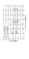
上記(1)〜(4)式をy=0、即ちアモルファスシリコン膜の膜厚を“0”としたとき、線I〜IVと堆積時間との交点を求めたものを図5及び図6に示す。なお、図5は図3中の破線枠A内を拡大した拡大図、図6は図4中の破線枠B内を拡大した拡大図に相当する。 FIG. 5 and FIG. 6 show the intersections of the lines I to IV and the deposition time when the above equations (1) to (4) are set to y = 0, that is, the film thickness of the amorphous silicon film is “0”. Show. 5 corresponds to an enlarged view in which the inside of the broken line frame A in FIG. 3 is enlarged, and FIG. 6 corresponds to an enlarged view in which the inside of the broken line frame B in FIG. 4 is enlarged.
図5に示すように、下地2がプリフロー有りのシリコン酸化膜のとき、アモルファスシリコン膜4の堆積が、処理開始から約1.2min(x≒1.189)から始まるのに対して、プリフロー無しのシリコン酸化膜のときには、アモルファスシリコン膜4の堆積が、処理開始から約2.0min(x≒1.984)から始まる。 As shown in FIG. 5, when the silicon oxide film underlying 2 preflow There, deposition of the amorphous silicon film 4 is, for though starting from about 1.2min from treatment initiation (x ≒ 1.189), no pre-flow In the case of the silicon oxide film, the deposition of the amorphous silicon film 4 starts from about 2.0 min (x≈1.984) from the start of the process.
図9に、原子間力顕微鏡(AFM)を用いて測定したアモルファスシリコン膜表面の平均面粗さ(表面ラフネス)Raを示す。図9に示す結果においては、AFMのスキャンサイズを1μm、スキャンレートを1.993Hzに設定した。 FIG. 9 shows an average surface roughness (surface roughness) Ra of the amorphous silicon film surface measured using an atomic force microscope (AFM). In the results shown in FIG. 9, the AFM scan size was set to 1 μm and the scan rate was set to 1.993 Hz.
図9に示すように、アミノシラン系ガスのプリフロー有りの場合、プリフロー無しに比較して、膜厚50nm以上膜厚100nm以下の範囲において、平均面粗さ(表面ラフネス)Raが0.101〜0.157nm改善されていることが分かった。このAFMによる測定結果から、一実施形態に係るアモルファスシリコン膜の成膜方法は、特に、アモルファスシリコン膜の膜厚が薄い場合に、プリフロー無しに比較して平均面粗さ(表面ラフネス)Raの改善効果が高いことが判明した。例えば、膜厚が約50nmのアモルファスシリコン膜においては、プリフロー無しの場合、Ra=0.411であったのに対し、プリフロー有りの場合にはRa=0.254と、Raが0.157nm改善されている。この結果は、一実施形態に係るアモルファスシリコン膜の成膜方法が、例えば、半導体装置の微細化が進展すれば進展するほど、有効であることを示している。 As shown in FIG. 9, when the aminosilane-based gas is preflowed , the average surface roughness (surface roughness) Ra is 0.101 to 0 in the range of the film thickness of 50 nm or more and 100 nm or less as compared with the case without preflow. It was found to be improved by 157 nm. From the measurement result by this AFM, the film formation method of the amorphous silicon film according to one embodiment has an average surface roughness (surface roughness) Ra as compared with the case of no preflow particularly when the film thickness of the amorphous silicon film is thin. It was found that the improvement effect was high. For example, in an amorphous silicon film having a film thickness of about 50 nm, Ra = 0.411 when there was no preflow, whereas Ra = 0.254 when Ra was preflowed, and Ra was improved by 0.157 nm. Has been. This result indicates that the amorphous silicon film forming method according to the embodiment is more effective as the semiconductor device is further miniaturized.
アモルファスシリコン膜4の表面ラフネスが大きい場合には、図12Aに示すように、接触部6に大きなボイド7が発生するのに対して、一実施形態に係る成膜方法を利用して形成された表面ラフネスが小さいアモルファスシリコン膜4によれば、図12Bに示すように、接触部6に発生するボイド7は小さくなる。ボイド7が小さくなれば、コンタクトホール5の内部に埋め込まれたアモルファスシリコン膜4の抵抗値の増大を抑制することができる。 If the surface roughness of the amorphous silicon film 4 is large, as shown in FIG. 12A, for although large voids 7 in the contact portion 6 is produced, which is formed by using a film forming method according to an embodiment According to the amorphous silicon film 4 having a small surface roughness, the void 7 generated in the contact portion 6 is small as shown in FIG. 12B. If the void 7 is reduced, an increase in the resistance value of the amorphous silicon film 4 embedded in the contact hole 5 can be suppressed.
また、上記実施形態に記載した成膜方法は、表面ラフネス、例えば、平均面粗さRaを0.1nmオーダーで改善できるものであるから、半導体装置の製造プロセスに好適である。
また、シード層3は、厚くするとアモルファスシリコン膜4の膜厚を増加させ、半導体装置の微細化を損なうことになる。また、シード層3は、アモルファスシリコンの核を均一に発生させるものである。このため、シード層3の厚さは薄いことが望ましく、好ましくは単原子層レベルの厚さ程度であることが良い。具体的なシード層3の厚さを言及すれば、0.1nm以上0.3nm以下であることが良い。
Further, the film forming method described in the above embodiment can improve the surface roughness, for example, the average surface roughness Ra on the order of 0.1 nm, and thus is suitable for the manufacturing process of the semiconductor device.
Further, if the seed layer 3 is thickened, the thickness of the amorphous silicon film 4 is increased and the miniaturization of the semiconductor device is impaired. The seed layer 3 is for uniformly generating nuclei of amorphous silicon. For this reason, it is desirable that the thickness of the seed layer 3 is small, and it is preferable that the thickness is about the monoatomic layer level. If a specific thickness of the seed layer 3 is mentioned, it is preferable that the thickness be 0.1 nm or more and 0.3 nm or less.
また、アモルファスシリコン膜4の厚さは、上記一実施形態の開示から、50nm以上100nm以下であることが好ましいが、例えば、50nm以下100nm以上の範囲の厚さとすることも可能である。 The thickness of the amorphous silicon film 4, from the disclosure of the above embodiment, but it is preferably 50nm or more 100nm or less, for example, it is possible to a thickness in the range of 1 00 nm or more below 50nm.
さらに、アミノシラン系ガスとアミノ基を含まないシラン系ガス(シリコンソース)との組み合わせを考慮した場合には、アミノシラン系ガスが熱分解する温度の近辺で熱分解しやすいモノシラン(SiH4)、ジシラン(Si 2 H6)が良い。
その他、この発明はその要旨を逸脱しない範囲で様々に変形することができる。
Furthermore, when considering the combination of an aminosilane-based gas and a silane-based gas (silicon source) that does not contain an amino group, monosilane (SiH 4 ), disilane that is easily thermally decomposed near the temperature at which the aminosilane-based gas is thermally decomposed. (Si 2 H 6 ) is preferable.
In addition, the present invention can be variously modified without departing from the gist thereof.
Claims (14)
(1) 前記下地を加熱し、前記加熱した下地にアミノシラン系ガスを流し、前記下地表面にシード層を形成する工程と、
(2) 前記下地を加熱し、前記加熱した下地表面のシード層にアミノ基を含まないシラン系ガスを供給し、前記アミノ基を含まないシラン系ガスを熱分解させることで、前記シード層上にアモルファスシリコン膜を形成する工程と、
を備えることを特徴とするアモルファスシリコン膜の成膜方法。 A film forming method for forming a film including an amorphous silicon film on the ground,
(1) heating the base, flowing an aminosilane-based gas over the heated base, and forming a seed layer on the base surface;
(2) heating the base, supplying a silane-based gas not containing an amino group to the seed layer on the heated base surface, and thermally decomposing the silane-based gas not containing the amino group; Forming an amorphous silicon film on the substrate,
A method for forming an amorphous silicon film, comprising:
前記(1)工程における前記シード層を形成するための処理時間が、前記(2)工程における前記アモルファスシリコン膜を形成するための処理時間よりも短いことを特徴とする請求項1に記載のアモルファスシリコン膜の成膜方法。 The heating temperature of the base in the step (1) is lower than the heating temperature of the base in the step (2),
2. The amorphous state according to claim 1, wherein a processing time for forming the seed layer in the step (1) is shorter than a processing time for forming the amorphous silicon film in the step (2). A method for forming a silicon film.
BAS(ブチルアミノシラン)
BTBAS(ビスターシャリブチルアミノシラン)
DMAS(ジメチルアミノシラン)
BDMAS(ビスジメチルアミノシラン)
TDMAS(トリスジメチルアミノシラン)
DEAS(ジエチルアミノシラン)
BDEAS(ビスジエチルアミノシラン)
DPAS(ジプロピルアミノシラン)、及び
DIPAS(ジイソプロピルアミノシラン)
の少なくとも一つを含むガスから選ばれ、
前記アミノ基を含まないシラン系ガスが、
SiH 4
Si2H6
SimH2m+2(ただし、mは3以上の自然数)の式で表されるシリコンの水素化物、及び
SinH2n(ただし、nは3以上の自然数)の式で表されるシリコンの水素化物
の少なくとも一つを含むガスから選ばれることを特徴とする請求項1から請求項4のいずれか一項に記載のアモルファスシリコン膜の成膜方法。 The aminosilane-based gas is
BAS (Butylaminosilane)
BTBAS (Bicter Shaftybutylaminosilane)
DMAS (dimethylaminosilane)
BDMAS (Bisdimethylaminosilane)
TDMAS (tri scan dimethylamino silane)
DEAS (diethylaminosilane)
BDEAS (Bisdiethylaminosilane)
DPAS (dipropylaminosilane) and DIPAS (diisopropylaminosilane)
Selected from gases containing at least one of
Silane-based gas containing no said amino group,
S iH 4
S i 2 H 6
Si hydride represented by the formula Si m H 2m + 2 (where m is a natural number of 3 or more), and hydride of silicon represented by the formula Si n H 2n (where n is a natural number of 3 or more) The method for forming an amorphous silicon film according to claim 1, wherein the film is selected from a gas containing at least one of the following.
DIPAS(ジイソプロピルアミノシラン)DIPAS (Diisopropylaminosilane)
であり、And
前記アミノ基を含まないシラン系ガスが、The silane-based gas containing no amino group is
SiHSiH 44
SiSi 22 HH 66
のいずれか一つから選ばれることを特徴とする請求項1から請求項4のいずれか一項に記載のアモルファスシリコン膜の成膜方法。5. The method for forming an amorphous silicon film according to claim 1, wherein the film is selected from any one of the following.
TDMAS(トリスジメチルアミノシラン)TDMAS (Trisdimethylaminosilane)
DEAS(ジエチルアミノシラン)DEAS (diethylaminosilane)
のいずれか一つから選ばれ、Selected from one of
前記アミノ基を含まないシラン系ガスが、The silane-based gas containing no amino group is
SiHSiH 44
SiSi 22 HH 66
のいずれか一つから選ばれることを特徴とする請求項1から請求項4のいずれか一項に記載のアモルファスシリコン膜の成膜方法。5. The method for forming an amorphous silicon film according to claim 1, wherein the film is selected from any one of the following.
トリシラン(Si3H8)
テトラシラン(Si4H10)
ペンタシラン(Si5H12)
ヘキサシラン(Si6H14)
ヘプタシラン(Si7H16)
の少なくとも一つから選ばれ、
前記SinH2n(ただし、nは3以上の自然数)の式で表されるシリコンの水素化物が、
シクロトリシラン(Si3H6)
シクロテトラシラン(Si4H8)
シクロペンタシラン(Si5H10)
シクロヘキサシラン(Si6H12)
シクロヘプタシラン(Si7H14)
の少なくともいずれか一つから選ばれることを特徴とする請求項5に記載のアモルファスシリコン膜の成膜方法。 A silicon hydride represented by the formula of Si m H 2m + 2 (where m is a natural number of 3 or more),
Trisilane (Si 3 H 8 )
Tetrasilane (Si 4 H 10 )
Pentasilane (Si 5 H 12 )
Hexasilane (Si 6 H 14 )
Heptasilane (Si 7 H 16 )
Selected from at least one of
A silicon hydride represented by the formula of Si n H 2n (where n is a natural number of 3 or more) is:
Cyclotrisilane (Si 3 H 6 )
Cyclotetrasilane (Si 4 H 8 )
Cyclopentasilane (Si 5 H 10 )
Cyclohexasilane (Si 6 H 12 )
Cycloheptasilane (Si 7 H 14 )
The method for forming an amorphous silicon film according to claim 5 , wherein the film is selected from at least one of the following.
前記アモルファスシリコン膜が形成される下地を有した被処理体を収容する処理室と、
前記処理室内に、処理に使用するガスを供給する処理ガス供給機構と、
前記処理室内に収容された前記被処理体を加熱する加熱装置と、
前記処理室内を排気する排気機構と、
前記処理ガス供給機構、前記加熱装置、及び前記排気機構を制御するコントローラと、を具備し、
前記コントローラが、請求項1に記載された(1)工程及び(2)工程が実施されるように前記処理ガス供給機構、前記加熱装置、及び前記排気機構を制御することを特徴とする成膜装置。 A film forming apparatus for forming an amorphous silicon film on the ground,
A processing chamber containing a target object having a base on which the amorphous silicon film is formed;
A processing gas supply mechanism for supplying a gas used for processing into the processing chamber;
A heating device for heating the object to be processed accommodated in the processing chamber;
An exhaust mechanism for exhausting the processing chamber;
A controller for controlling the processing gas supply mechanism, the heating device, and the exhaust mechanism,
The controller controls the processing gas supply mechanism, the heating device, and the exhaust mechanism so that the steps (1) and (2) described in claim 1 are performed. apparatus.
Priority Applications (15)
| Application Number | Priority Date | Filing Date | Title |
|---|---|---|---|
| JP2011044014A JP4967066B2 (en) | 2010-04-27 | 2011-03-01 | Method and apparatus for forming amorphous silicon film |
| TW102134148A TWI562202B (en) | 2010-04-27 | 2011-04-25 | Amorphous silicon film formation method and amorphous silicon film formation apparatus |
| TW100114311A TWI420574B (en) | 2010-04-27 | 2011-04-25 | Amorphous silicon film formation method and amorphous silicon film formation apparatus |
| US13/094,043 US9006021B2 (en) | 2010-04-27 | 2011-04-26 | Amorphous silicon film formation method and amorphous silicon film formation apparatus |
| KR1020110039227A KR101282908B1 (en) | 2010-04-27 | 2011-04-26 | Amorphous silicon film formation method and amorphous silicon film formation apparatus |
| CN201410478548.7A CN104278252B (en) | 2010-04-27 | 2011-04-27 | Amorphous silicon film formation method and amorphous silicon film formation apparatus |
| CN201410479712.6A CN104264125B (en) | 2010-04-27 | 2011-04-27 | Film formation device |
| CN201410478007.4A CN104264124B (en) | 2010-04-27 | 2011-04-27 | Film formation device |
| CN201110107275.1A CN102234786B (en) | 2010-04-27 | 2011-04-27 | Amorphous silicon film formation method and amorphous silicon film formation apparatus |
| KR1020120145412A KR101529171B1 (en) | 2010-04-27 | 2012-12-13 | Amorphous silicon film formation method and amorphous silicon film formation apparatus |
| KR1020140072194A KR101534638B1 (en) | 2010-04-27 | 2014-06-13 | Amorphous silicon film formation method and amorphous silicon film formation apparatus |
| KR1020140072193A KR101534637B1 (en) | 2010-04-27 | 2014-06-13 | Amorphous silicon film formation method and amorphous silicon film formation apparatus |
| KR1020140072197A KR101615968B1 (en) | 2010-04-27 | 2014-06-13 | Amorphous silicon film formation method and amorphous silicon film formation apparatus |
| KR1020140072192A KR101534634B1 (en) | 2010-04-27 | 2014-06-13 | Amorphous silicon film formation method and amorphous silicon film formation apparatus |
| US14/656,914 US9123782B2 (en) | 2010-04-27 | 2015-03-13 | Amorphous silicon film formation method and amorphous silicon film formation apparatus |
Applications Claiming Priority (3)
| Application Number | Priority Date | Filing Date | Title |
|---|---|---|---|
| JP2010102405 | 2010-04-27 | ||
| JP2010102405 | 2010-04-27 | ||
| JP2011044014A JP4967066B2 (en) | 2010-04-27 | 2011-03-01 | Method and apparatus for forming amorphous silicon film |
Related Child Applications (5)
| Application Number | Title | Priority Date | Filing Date |
|---|---|---|---|
| JP2012084170A Division JP5330562B2 (en) | 2010-04-27 | 2012-04-02 | Deposition equipment |
| JP2012084169A Division JP5337269B2 (en) | 2010-04-27 | 2012-04-02 | Method and apparatus for forming amorphous silicon film |
| JP2012084172A Division JP5330563B2 (en) | 2010-04-27 | 2012-04-02 | Deposition equipment |
| JP2012084168A Division JP5373142B2 (en) | 2010-04-27 | 2012-04-02 | Method and apparatus for forming amorphous silicon film |
| JP2012084171A Division JP5373143B2 (en) | 2010-04-27 | 2012-04-02 | Method for manufacturing semiconductor device and method for filling contact hole and / or line |
Publications (3)
| Publication Number | Publication Date |
|---|---|
| JP2011249764A JP2011249764A (en) | 2011-12-08 |
| JP2011249764A5 true JP2011249764A5 (en) | 2012-01-26 |
| JP4967066B2 JP4967066B2 (en) | 2012-07-04 |
Family
ID=44816157
Family Applications (1)
| Application Number | Title | Priority Date | Filing Date |
|---|---|---|---|
| JP2011044014A Active JP4967066B2 (en) | 2010-04-27 | 2011-03-01 | Method and apparatus for forming amorphous silicon film |
Country Status (5)
| Country | Link |
|---|---|
| US (2) | US9006021B2 (en) |
| JP (1) | JP4967066B2 (en) |
| KR (6) | KR101282908B1 (en) |
| CN (4) | CN104264124B (en) |
| TW (2) | TWI562202B (en) |
Families Citing this family (45)
| Publication number | Priority date | Publication date | Assignee | Title |
|---|---|---|---|---|
| JP4967066B2 (en) * | 2010-04-27 | 2012-07-04 | 東京エレクトロン株式会社 | Method and apparatus for forming amorphous silicon film |
| JP5330563B2 (en) * | 2010-04-27 | 2013-10-30 | 東京エレクトロン株式会社 | Deposition equipment |
| JP5490753B2 (en) * | 2010-07-29 | 2014-05-14 | 東京エレクトロン株式会社 | Trench filling method and film forming system |
| JP5544343B2 (en) * | 2010-10-29 | 2014-07-09 | 東京エレクトロン株式会社 | Deposition equipment |
| JP5689398B2 (en) * | 2010-12-21 | 2015-03-25 | 東京エレクトロン株式会社 | Method and apparatus for forming silicon nitride film |
| JP5675331B2 (en) * | 2010-12-27 | 2015-02-25 | 東京エレクトロン株式会社 | How to fill trench |
| JP5977002B2 (en) * | 2011-08-25 | 2016-08-24 | 東京エレクトロン株式会社 | Trench filling method and semiconductor integrated circuit device manufacturing method |
| US9353442B2 (en) | 2011-10-28 | 2016-05-31 | Tokyo Electron Limited | Apparatus for forming silicon-containing thin film |
| JP5829196B2 (en) * | 2011-10-28 | 2015-12-09 | 東京エレクトロン株式会社 | Method for forming silicon oxide film |
| JP5793398B2 (en) * | 2011-10-28 | 2015-10-14 | 東京エレクトロン株式会社 | Method for forming seed layer and method for forming silicon-containing thin film |
| JP5780981B2 (en) * | 2012-03-02 | 2015-09-16 | 東京エレクトロン株式会社 | Method for forming germanium thin film |
| JP5792101B2 (en) | 2012-03-15 | 2015-10-07 | 東京エレクトロン株式会社 | Method for forming laminated semiconductor film |
| KR101862547B1 (en) * | 2012-04-13 | 2018-05-31 | 삼성전자주식회사 | Method of forming a polysilicon layer and method of manufactruing semiconductir devices |
| JP6022273B2 (en) * | 2012-09-14 | 2016-11-09 | 株式会社日立国際電気 | Semiconductor device manufacturing method, substrate processing method, substrate processing apparatus, and program |
| JP6022272B2 (en) | 2012-09-14 | 2016-11-09 | 株式会社日立国際電気 | Semiconductor device manufacturing method, substrate processing apparatus, and program |
| JP5876398B2 (en) * | 2012-10-18 | 2016-03-02 | 東京エレクトロン株式会社 | Film forming method and film forming apparatus |
| JP6068130B2 (en) | 2012-12-25 | 2017-01-25 | 株式会社日立国際電気 | Semiconductor device manufacturing method, substrate processing apparatus, and program |
| JP5947710B2 (en) * | 2012-12-27 | 2016-07-06 | 東京エレクトロン株式会社 | Seed layer forming method, silicon film forming method and film forming apparatus |
| JP5925673B2 (en) | 2012-12-27 | 2016-05-25 | 東京エレクトロン株式会社 | Silicon film forming method and film forming apparatus |
| JP6125279B2 (en) | 2013-03-05 | 2017-05-10 | 株式会社日立国際電気 | Semiconductor device manufacturing method, substrate processing apparatus, and program |
| JP6082712B2 (en) * | 2013-07-31 | 2017-02-15 | 東京エレクトロン株式会社 | Silicon film forming method and thin film forming method |
| JP6092040B2 (en) * | 2013-08-02 | 2017-03-08 | 東京エレクトロン株式会社 | Silicon film forming method and apparatus therefor |
| KR101489306B1 (en) * | 2013-10-21 | 2015-02-11 | 주식회사 유진테크 | Amorphous silicon film formation method and amorphous silicon film formation apparatus |
| JP6348707B2 (en) * | 2013-12-11 | 2018-06-27 | 東京エレクトロン株式会社 | Amorphous silicon crystallization method, crystallized silicon film formation method, semiconductor device manufacturing method, and film formation apparatus |
| KR101507381B1 (en) * | 2014-02-26 | 2015-03-30 | 주식회사 유진테크 | Method for forming polycrystalline silicon film |
| KR20150108664A (en) * | 2014-03-18 | 2015-09-30 | 주식회사 유진테크 머티리얼즈 | precursor compounds and thin film deposition method using the precusor compoumds |
| JP2015192063A (en) * | 2014-03-28 | 2015-11-02 | 東京エレクトロン株式会社 | Cleaning method of amorphous silicon film formation device, formation method of amorphous silicon film and amorphous silicon film formation device |
| US20150303060A1 (en) * | 2014-04-16 | 2015-10-22 | Samsung Electronics Co., Ltd. | Silicon precursor, method of forming a layer using the same, and method of fabricating semiconductor device using the same |
| US9915001B2 (en) | 2014-09-03 | 2018-03-13 | Silcotek Corp. | Chemical vapor deposition process and coated article |
| SG10201506694QA (en) * | 2014-09-03 | 2016-04-28 | Silcotek Corp | Chemical vapor deposition process and coated article |
| KR102334110B1 (en) * | 2014-10-24 | 2021-12-02 | 삼성전자주식회사 | Method of forming a semiconductor device |
| KR101706747B1 (en) * | 2015-05-08 | 2017-02-15 | 주식회사 유진테크 | Method for forming amorphous thin film |
| JP6086942B2 (en) | 2015-06-10 | 2017-03-01 | 株式会社日立国際電気 | Semiconductor device manufacturing method, substrate processing apparatus, and program |
| US10876206B2 (en) | 2015-09-01 | 2020-12-29 | Silcotek Corp. | Thermal chemical vapor deposition coating |
| TWI716511B (en) * | 2015-12-19 | 2021-01-21 | 美商應用材料股份有限公司 | Conformal amorphous silicon as nucleation layer for w ald process |
| JP6368743B2 (en) * | 2016-06-22 | 2018-08-01 | 株式会社日立国際電気 | Substrate processing apparatus, semiconductor device manufacturing method, and program |
| JP6613213B2 (en) | 2016-07-26 | 2019-11-27 | 株式会社Kokusai Electric | Semiconductor device manufacturing method, substrate processing apparatus, and program |
| CN106282963B (en) * | 2016-09-21 | 2019-04-05 | 中国科学院上海微系统与信息技术研究所 | Amorphous silicon growing method and device based on magnetic interference plasma |
| JP6902958B2 (en) | 2017-08-02 | 2021-07-14 | 東京エレクトロン株式会社 | Silicon film forming method and forming device |
| JP7065728B2 (en) * | 2018-08-17 | 2022-05-12 | 東京エレクトロン株式会社 | Film formation method and film formation equipment |
| JP7018849B2 (en) * | 2018-08-17 | 2022-02-14 | 東京エレクトロン株式会社 | Film formation method and film formation equipment |
| JP7190875B2 (en) * | 2018-11-16 | 2022-12-16 | 東京エレクトロン株式会社 | Polysilicon film forming method and film forming apparatus |
| WO2020252306A1 (en) | 2019-06-14 | 2020-12-17 | Silcotek Corp. | Nano-wire growth |
| JP2022143997A (en) * | 2021-03-18 | 2022-10-03 | キオクシア株式会社 | Semiconductor manufacturing method and semiconductor manufacturing apparatus |
| JP2022160317A (en) * | 2021-04-06 | 2022-10-19 | 東京エレクトロン株式会社 | Film forming method and film forming device of silicon film |
Family Cites Families (27)
| Publication number | Priority date | Publication date | Assignee | Title |
|---|---|---|---|---|
| US4671970A (en) * | 1986-02-05 | 1987-06-09 | Ncr Corporation | Trench filling and planarization process |
| JPS6329954A (en) | 1986-07-23 | 1988-02-08 | Toshiba Corp | Manufacture of semiconductor device |
| JP2835723B2 (en) * | 1988-02-26 | 1998-12-14 | 富士通株式会社 | Capacitor and method of manufacturing capacitor |
| JPH0427116A (en) | 1990-05-23 | 1992-01-30 | Fujitsu Ltd | Method of forming semiconductor heterojunction |
| JP3194256B2 (en) | 1991-11-14 | 2001-07-30 | 富士通株式会社 | Film growth method and film growth apparatus |
| US5856236A (en) | 1996-06-14 | 1999-01-05 | Micron Technology, Inc. | Method of depositing a smooth conformal aluminum film on a refractory metal nitride layer |
| US6333066B1 (en) * | 1997-11-21 | 2001-12-25 | Samsung Electronics Co., Ltd. | Method for forming PZT thin film using seed layer |
| KR100494321B1 (en) | 1997-12-31 | 2005-08-31 | 주식회사 하이닉스반도체 | Polycrystalline Silicon Film Formation Method of Semiconductor Device |
| KR100611473B1 (en) | 2000-12-29 | 2006-08-09 | 주식회사 하이닉스반도체 | Method of manufacturing a semiconductor device |
| JP2004253778A (en) * | 2003-01-30 | 2004-09-09 | Nec Electronics Corp | Semiconductor device and its manufacturing method |
| CN1630036A (en) | 2003-12-17 | 2005-06-22 | 旺宏电子股份有限公司 | Semiconductor component and method of forming polysilicon layer therein |
| KR100611108B1 (en) * | 2005-01-13 | 2006-08-09 | 삼성전자주식회사 | Method of manufacturing a thin film layer |
| JP4761041B2 (en) * | 2005-02-23 | 2011-08-31 | ソニー株式会社 | Method for forming silicon film |
| JP4228150B2 (en) * | 2005-03-23 | 2009-02-25 | 東京エレクトロン株式会社 | Film forming apparatus, film forming method, and storage medium |
| US7566655B2 (en) * | 2005-05-26 | 2009-07-28 | Applied Materials, Inc. | Integration process for fabricating stressed transistor structure |
| CN101208783B (en) * | 2005-05-26 | 2010-05-19 | 应用材料股份有限公司 | Method to increase silicon nitride film tensile stress using post PECVD deposition and UV processing |
| US7601652B2 (en) * | 2005-06-21 | 2009-10-13 | Applied Materials, Inc. | Method for treating substrates and films with photoexcitation |
| KR101014858B1 (en) * | 2006-03-30 | 2011-02-15 | 미쯔이 죠센 가부시키가이샤 | Method and apparatus for growing plasma atomic layer |
| JP5311791B2 (en) * | 2007-10-12 | 2013-10-09 | 東京エレクトロン株式会社 | Method for forming polysilicon film |
| US20090104733A1 (en) * | 2007-10-22 | 2009-04-23 | Yong Kee Chae | Microcrystalline silicon deposition for thin film solar applications |
| JP5248995B2 (en) * | 2007-11-30 | 2013-07-31 | 株式会社半導体エネルギー研究所 | Method for manufacturing photoelectric conversion device |
| JP5286046B2 (en) * | 2007-11-30 | 2013-09-11 | 株式会社半導体エネルギー研究所 | Method for manufacturing photoelectric conversion device |
| CN101609796B (en) * | 2008-06-20 | 2012-03-21 | 福建钧石能源有限公司 | Film forming method and method for manufacturing film solar battery |
| JP5495847B2 (en) * | 2010-02-24 | 2014-05-21 | 株式会社日立国際電気 | Semiconductor device manufacturing method, substrate processing apparatus, and substrate processing method |
| JP2011216784A (en) * | 2010-04-01 | 2011-10-27 | Hitachi Kokusai Electric Inc | Method of manufacturing semiconductor device and substrate processing apparatus |
| US20110263074A1 (en) * | 2010-04-22 | 2011-10-27 | Applied Materials, Inc. | Apparatus and methods for reducing light induced damage in thin film solar cells |
| JP4967066B2 (en) * | 2010-04-27 | 2012-07-04 | 東京エレクトロン株式会社 | Method and apparatus for forming amorphous silicon film |
-
2011
- 2011-03-01 JP JP2011044014A patent/JP4967066B2/en active Active
- 2011-04-25 TW TW102134148A patent/TWI562202B/en active
- 2011-04-25 TW TW100114311A patent/TWI420574B/en active
- 2011-04-26 KR KR1020110039227A patent/KR101282908B1/en active IP Right Grant
- 2011-04-26 US US13/094,043 patent/US9006021B2/en active Active
- 2011-04-27 CN CN201410478007.4A patent/CN104264124B/en active Active
- 2011-04-27 CN CN201410479712.6A patent/CN104264125B/en active Active
- 2011-04-27 CN CN201110107275.1A patent/CN102234786B/en active Active
- 2011-04-27 CN CN201410478548.7A patent/CN104278252B/en active Active
-
2012
- 2012-12-13 KR KR1020120145412A patent/KR101529171B1/en active IP Right Grant
-
2014
- 2014-06-13 KR KR1020140072194A patent/KR101534638B1/en active IP Right Grant
- 2014-06-13 KR KR1020140072192A patent/KR101534634B1/en active IP Right Grant
- 2014-06-13 KR KR1020140072193A patent/KR101534637B1/en active IP Right Grant
- 2014-06-13 KR KR1020140072197A patent/KR101615968B1/en active IP Right Grant
-
2015
- 2015-03-13 US US14/656,914 patent/US9123782B2/en active Active
Similar Documents
| Publication | Publication Date | Title |
|---|---|---|
| JP2011249764A5 (en) | ||
| JP4967066B2 (en) | Method and apparatus for forming amorphous silicon film | |
| JP5741382B2 (en) | Thin film forming method and film forming apparatus | |
| JP6585551B2 (en) | Semiconductor device manufacturing method, substrate processing apparatus, and program | |
| KR101775950B1 (en) | Method and apparatus for forming amorphous silicon film | |
| JP5827384B2 (en) | Method and apparatus for forming amorphous silicon film | |
| JP2009152551A5 (en) | ||
| JP5925673B2 (en) | Silicon film forming method and film forming apparatus | |
| TWI609982B (en) | Method of forming germanium film and apparatus therefor | |
| JP5854112B2 (en) | Thin film forming method and film forming apparatus | |
| JP5710819B2 (en) | Method and apparatus for forming amorphous silicon film | |
| JP6010161B2 (en) | Method and apparatus for forming amorphous silicon film | |
| TWI627677B (en) | Method for forming amorphous thin film |