JP2011199975A - Device, system and method for noncontact power transmission - Google Patents
Device, system and method for noncontact power transmission Download PDFInfo
- Publication number
- JP2011199975A JP2011199975A JP2010062307A JP2010062307A JP2011199975A JP 2011199975 A JP2011199975 A JP 2011199975A JP 2010062307 A JP2010062307 A JP 2010062307A JP 2010062307 A JP2010062307 A JP 2010062307A JP 2011199975 A JP2011199975 A JP 2011199975A
- Authority
- JP
- Japan
- Prior art keywords
- power transmission
- circuit
- power
- circuits
- oscillation
- Prior art date
- Legal status (The legal status is an assumption and is not a legal conclusion. Google has not performed a legal analysis and makes no representation as to the accuracy of the status listed.)
- Pending
Links
- 230000005540 biological transmission Effects 0.000 title claims abstract description 513
- 238000000034 method Methods 0.000 title claims description 17
- 230000010355 oscillation Effects 0.000 claims abstract description 200
- 239000003990 capacitor Substances 0.000 claims abstract description 47
- 239000011159 matrix material Substances 0.000 claims abstract description 12
- 238000001514 detection method Methods 0.000 claims description 32
- 230000003111 delayed effect Effects 0.000 claims description 8
- 230000007274 generation of a signal involved in cell-cell signaling Effects 0.000 claims description 4
- 230000001934 delay Effects 0.000 claims description 3
- 230000015572 biosynthetic process Effects 0.000 abstract 1
- 230000008878 coupling Effects 0.000 description 33
- 238000010168 coupling process Methods 0.000 description 33
- 238000005859 coupling reaction Methods 0.000 description 33
- 238000010586 diagram Methods 0.000 description 27
- 102100040862 Dual specificity protein kinase CLK1 Human genes 0.000 description 13
- 230000001360 synchronised effect Effects 0.000 description 9
- 238000005259 measurement Methods 0.000 description 6
- 230000007423 decrease Effects 0.000 description 4
- 238000002347 injection Methods 0.000 description 4
- 239000007924 injection Substances 0.000 description 4
- 102100040844 Dual specificity protein kinase CLK2 Human genes 0.000 description 3
- 102100040856 Dual specificity protein kinase CLK3 Human genes 0.000 description 3
- 101000749294 Homo sapiens Dual specificity protein kinase CLK1 Proteins 0.000 description 3
- 101000749291 Homo sapiens Dual specificity protein kinase CLK2 Proteins 0.000 description 3
- 101000749304 Homo sapiens Dual specificity protein kinase CLK3 Proteins 0.000 description 3
- 238000013459 approach Methods 0.000 description 3
- 230000003071 parasitic effect Effects 0.000 description 2
- 238000007796 conventional method Methods 0.000 description 1
- 230000003247 decreasing effect Effects 0.000 description 1
- 238000005516 engineering process Methods 0.000 description 1
- 238000012545 processing Methods 0.000 description 1
- 238000004088 simulation Methods 0.000 description 1
- 235000013599 spices Nutrition 0.000 description 1
- 238000010408 sweeping Methods 0.000 description 1
Images


Landscapes
- Near-Field Transmission Systems (AREA)
Abstract
Description
本発明は、受電回路への電力供給を電磁共鳴を用いて非接触で行う技術に係り、特にフェイズドアレイコイルを用いて受電回路への電力供給を行う非接触送電装置、非接触送電システムおよび非接触送電方法に関するものである。 The present invention relates to a technique for performing power supply to a power receiving circuit in a contactless manner using electromagnetic resonance, and in particular, a contactless power transmission apparatus, a contactless power transmission system, and a non-contact power supply that supplies power to the power receiving circuit using a phased array coil. The present invention relates to a contact power transmission method.
従来より、受電回路への電力供給を電磁共鳴を用いて非接触で行う技術が知られている(特許文献1、特許文献2、特許文献3、特許文献4参照)。
特許文献1に開示された技術は、平面状コイルとコンデンサとからなる共振ユニットを非接触ICカードに複数設け、複数の共振ユニットの各共振周波数を、読み書き装置との間で、電力の伝達を行うのに必要な周波数よりも多少上下にシフトさせて、非接触ICカードの共振周波数を広帯域化したものである。
2. Description of the Related Art Conventionally, techniques for performing power supply to a power receiving circuit in a contactless manner using electromagnetic resonance are known (see
In the technology disclosed in
特許文献2に開示された技術は、送電コイルと受電コイルとの距離に応じて、送電コイルから送信する電力のデューティ比を変化させることにより、受電部の出力電圧の変動を低減するようにしたものである。
The technique disclosed in
特許文献3に開示された技術は、走行レール上を移動する移動体に対して給電を行うものである。 The technique disclosed in Patent Document 3 supplies power to a moving body that moves on a traveling rail.
特許文献4に開示された技術は、複数の送電コイルを給電装置に設け、被給電装置の置かれた位置に応じて、特定の送電コイルのみを選択的に駆動することにより、複数台の被給電装置に対して同時に給電を行うものである。 In the technique disclosed in Patent Document 4, a plurality of power transmission coils are provided in a power feeding device, and only a specific power transmission coil is selectively driven in accordance with a position where the power supplied device is placed, so that a plurality of power transmission coils are provided. Power is supplied to the power supply device at the same time.
特許文献1〜特許文献4に開示された技術では、伝送距離(送電コイルと受電コイル間の距離)の3乗に反比例してコイル間の磁気結合係数が低下するため、送電コイルおよび受電コイルの直径を大幅に超えるような長距離では送電効率が下がるという問題点があった。
In the techniques disclosed in
本発明は、上記課題を解決するためになされたもので、従来と比較して送電効率を改善することができる非接触送電装置、非接触送電システムおよび非接触送電方法を提供することを目的とする。 The present invention has been made to solve the above-described problem, and an object thereof is to provide a non-contact power transmission apparatus, a non-contact power transmission system, and a non-contact power transmission method that can improve power transmission efficiency as compared with the conventional art. To do.
本発明の非接触送電装置は、N(Nは2以上の整数)個の送電回路と、このN個の送電回路を制御する制御手段とを備え、前記送電回路は、直列に接続されたキャパシタと送電コイルとからなる送電側LCタンク回路と、この送電側LCタンク回路に電力を供給する発振回路とを有し、前記N個の送電回路の送電コイルは、マトリクス状に配置され、前記制御手段は、前記N個の送電回路の送電コイルのうち少なくとも2個の送電コイルから到達する磁場の変化の位相が受電回路の受電コイルにおいて揃うように、前記N個の送電回路の各発振回路が発生する信号の位相を制御することを特徴とするものである。 The non-contact power transmission apparatus of the present invention includes N (N is an integer of 2 or more) power transmission circuits and control means for controlling the N power transmission circuits, and the power transmission circuit includes capacitors connected in series. And a power transmission side LC tank circuit composed of a power transmission coil, and an oscillation circuit for supplying power to the power transmission side LC tank circuit, wherein the power transmission coils of the N power transmission circuits are arranged in a matrix, and the control The means is configured so that each oscillation circuit of the N power transmission circuits has a phase of a change in magnetic field reaching from at least two power transmission coils among the power transmission coils of the N power transmission circuits aligned in the power reception coil of the power reception circuit. The phase of the generated signal is controlled.
また、本発明の非接触送電システムは、非接触送電装置と、この非接触送電装置から電力供給を受ける受電回路とを備え、前記受電回路は、直列に接続されたキャパシタと受電コイルとからなる受電側LCタンク回路と、この受電側LCタンク回路に接続される負荷インピーダンスを変化させる負荷インピーダンス可変回路と、前記受電側LCタンク回路の出力に基づいて受信電力の強度を検出し、受信電力が最大になるように前記負荷インピーダンスを変化させる受信電力強度検出手段とを備えることを特徴とするものである。 The contactless power transmission system of the present invention includes a contactless power transmitting device and a power receiving circuit that receives power supply from the contactless power transmitting device, and the power receiving circuit includes a capacitor and a power receiving coil connected in series. The power receiving side LC tank circuit, the load impedance variable circuit for changing the load impedance connected to the power receiving side LC tank circuit, and the received power intensity are detected based on the output of the power receiving side LC tank circuit. Receiving power intensity detecting means for changing the load impedance so as to be maximized.
また、本発明の非接触送電システムは、非接触送電装置と、この非接触送電装置から電力供給を受ける受電回路とを備え、前記受電回路は、直列に接続されたキャパシタと受電コイルとからなる受電側LCタンク回路と、この受電側LCタンク回路の出力に基づいて受信電力の強度を検出し、検出した受信電力の強度の情報を前記非接触送電装置に無線送信する受信電力強度検出手段とを備え、前記送電回路は、前記受電回路から送信された情報を受信する受信手段を備え、前記制御手段は、前記受電回路から送信された情報に基づいて、前記受電回路の受信電力が最大になるように、少なくとも前記N個の送電回路の各発振回路が発生する信号の位相を制御することを特徴とするものである。 The contactless power transmission system of the present invention includes a contactless power transmitting device and a power receiving circuit that receives power supply from the contactless power transmitting device, and the power receiving circuit includes a capacitor and a power receiving coil connected in series. A power receiving side LC tank circuit, and a received power strength detecting means for detecting the strength of the received power based on the output of the power receiving side LC tank circuit and wirelessly transmitting the detected information on the strength of the received power to the non-contact power transmission device; The power transmission circuit includes reception means for receiving information transmitted from the power reception circuit, and the control means maximizes the received power of the power reception circuit based on the information transmitted from the power reception circuit. Thus, the phase of the signal generated by each oscillation circuit of at least the N power transmission circuits is controlled.
また、本発明は、直列に接続されたキャパシタと送電コイルとからなる送電側LCタンク回路と、この送電側LCタンク回路に電力を供給する発振回路とをそれぞれ備えたN(Nは2以上の整数)個の送電回路を用いて、受電回路への電力供給を行う非接触送電方法において、前記N個の送電回路の送電コイルは、マトリクス状に配置され、前記N個の送電回路の送電コイルのうち少なくとも2個の送電コイルから到達する磁場の変化の位相が前記受電回路の受電コイルにおいて揃うように、前記N個の送電回路の各発振回路が発生する信号の位相を制御することを特徴とするものである。 The present invention also includes a power transmission side LC tank circuit composed of a capacitor and a power transmission coil connected in series and an oscillation circuit that supplies power to the power transmission side LC tank circuit. In the non-contact power transmission method of supplying power to the power receiving circuit using an integer number of power transmission circuits, the power transmission coils of the N power transmission circuits are arranged in a matrix, and the power transmission coils of the N power transmission circuits The phase of the signal generated by each oscillation circuit of the N power transmission circuits is controlled so that the phase of the change in the magnetic field arriving from at least two of the power transmission coils is uniform in the power reception coils of the power reception circuit. It is what.
本発明によれば、N個の送電回路の送電コイルをマトリクス状に配置し、制御手段が、N個の送電回路の送電コイルのうち少なくとも2個の送電コイルから到達する磁場の変化の位相が受電回路の受電コイルにおいて揃うように、N個の送電回路の各発振回路が発生する信号の位相を制御することにより、磁場のビームフォーミングを行い、距離の離れた受電コイル近辺で磁場の強い変化を作ることができる。その結果、本発明では、電磁共鳴を用いた非接触送電システムにおいて、特に送電回路と受電回路との間の距離が遠い場合に、従来方式に比べて送電効率を改善することができる。また、本発明では、複数の受電回路に同時に送電することが可能になる。 According to the present invention, the power transmission coils of the N power transmission circuits are arranged in a matrix, and the control means has a phase change of the magnetic field reaching from at least two power transmission coils among the power transmission coils of the N power transmission circuits. By controlling the phase of the signal generated by each oscillation circuit of the N power transmission circuits so that they are aligned in the power reception coils of the power reception circuit, magnetic field beamforming is performed, and the magnetic field changes strongly in the vicinity of the power reception coil at a distance. Can be made. As a result, according to the present invention, in a contactless power transmission system using electromagnetic resonance, power transmission efficiency can be improved compared to the conventional method, particularly when the distance between the power transmission circuit and the power reception circuit is long. In the present invention, it is possible to transmit power to a plurality of power receiving circuits simultaneously.
[第1の実施の形態]
以下、本発明の実施の形態について図面を参照して説明する。図1は本発明の第1の実施の形態に係る非接触送電システムの構成を示すブロック図である。非接触送電システムは、非接触送電装置1と、非接触送電装置1から電力供給を受ける受電回路20とから構成される。
[First Embodiment]
Hereinafter, embodiments of the present invention will be described with reference to the drawings. FIG. 1 is a block diagram showing a configuration of a contactless power transmission system according to a first embodiment of the present invention. The contactless power transmission system includes a contactless
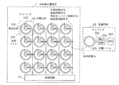
非接触送電装置1は、マトリクス状に配置されたN(Nは2以上の整数)個の送電回路10と、制御回路11とから構成される。送電回路10は、直列に接続された送電コイル101とキャパシタ102とを発振回路100の出力に接続したものである。N個の送電回路10をマトリクス状に配置することにより、N個の送電コイル101がマトリクス状に配置されることになる。制御回路11は、各送電回路10の発振回路100の発振のオン/オフ、発振周波数、発振の位相、発振信号の振幅などを制御する。
The non-contact
受電回路20は、受電コイル200と、受電コイル200と直列に接続されたキャパシタ201と、受電コイル200およびキャパシタ201と接続され、送電コイル101との電磁共鳴によって受電コイル200に生じた電力を整流する整流回路202と、整流回路202の出力に接続された負荷203とから構成される。
The
送電回路10は、送電コイル101とキャパシタ102によって固有の共振周波数を有している。同様に、受電回路20は、受電コイル200とキャパシタ201によって固有の共振周波数を有している。送電時には、送電回路10の共振周波数と受電回路20の共振周波数とを一致させる。
The
送電コイル101および受電コイル200のQ値(Quality Factor)は、自己インダクタンスL、共振周波数ω、寄生抵抗rを用いて、Q=ωL/rで表される。送電回路10の送電コイル101および受電回路20の受電コイル200のQ値は、100以上あることが望ましい。
Q values (Quality Factor) of the
また、少なくとも1つの送電回路10の送電コイル101と受電回路20の受電コイル200との間の結合係数kに対して、kと送電回路10の送電コイル101のQ値との積(kQ)が5以上あることが望ましい。その理由は、送電回路10の送電コイル101とキャパシタ102とで構成されるLCタンク回路の内に蓄えられたエネルギーのうち、kに比例した大きさのエネルギーが受電回路20の受電コイル200に伝播され、一方でLCタンク回路内のエネルギーのうち1/Qに比例した大きさのエネルギーが、ジュール熱などによって発散するためである。
Further, for a coupling coefficient k between the
熱などで発散するエネルギー以外はLCタンク回路内に留まり、送電コイル101と受電コイル200間のエネルギー伝送に寄与するので、系全体としてのエネルギー伝播効率はkQに比例する。したがって、kQの値を高くすることが、非接触送電システムにおいては肝要である。送電回路10の送電コイル101と受電回路20の受電コイル200とが密接している場合にはk値は1に近い値(ただし1未満)になる。
Since energy other than that dissipated by heat remains in the LC tank circuit and contributes to energy transmission between the
送電コイル101と受電コイル200間の距離が大きくなると徐々にk値は下がり、例えば、コイル101,200の直径と、送電コイル101と受電コイル200間の距離とが等しい場合に、k値は0.01から0.1の範囲の値となる。さらに送電コイル101と受電コイル200間の距離が大きくなると、k値は距離の−3乗に比例して小さくなる。
As the distance between the
したがって、送電コイル101に必要なQ値は受電コイル200との距離によって異なるが、実用的なk値を0.005〜0.05程度(送電コイル101と受電コイル200間の距離がコイル101,200の直径の1〜2倍に相当)で、kQの目安を5と仮定すると、送電コイル101に必要なQ値は100〜1000程度となる。
Therefore, although the Q value required for the
図2は本実施の形態の非接触送電システムにおいて、複数の送電回路10を用いて1つの受電回路20に電力を送電する場合の例を示す図である。図1で説明したとおり、各送電回路10(10−1〜10−3)は、発振回路100(100−1〜100−3)と、送電コイル101(101−1〜101−3)と、キャパシタ102(102−1〜102−3)とからなる。送電回路10の送電コイル101と受電回路20の受電コイル200との距離は、送電回路10によって異なる。図2の例では、送電回路10−1の送電コイル101−1と受電コイル200間の距離がl1、送電回路10−2の送電コイル101−2と受電コイル200間の距離がl2、送電回路10−3の送電コイル101−3と受電コイル200間の距離がl3である。
FIG. 2 is a diagram illustrating an example in the case where power is transmitted to one
受電回路20で受け取る電力の大きさを最大にするには、受電コイル200において、送電コイル101−1〜101−3から到達する磁場の変化の位相が揃っている必要がある。送電コイル101−1〜101−3の電流の変化が磁場の変化として受電コイル200に到達するまでには、それぞれ距離l1,l2,l3に比例した時間遅れが生じるので、発振回路100−1〜100−3が生成する信号の位相α,β,γを調整することで、この時間遅れを補償しなければならない。
In order to maximize the amount of power received by the
したがって、発振回路100−1〜100−3は、それぞれに接続された送電コイル101−1〜101−3と受電コイル200間の距離l1,l2,l3に比例した位相α,β,γを保ちながら、同じ周波数ωで発振する。すなわち、発振回路100−1は例えばsin{ω(t+α)}で表される信号を生成し、発振回路100−2はsin{ω(t+β)}で表される信号を生成し、発振回路100−3はsin{ω(t+γ)}で表される信号を生成する。
Therefore, the oscillation circuits 100-1 to 100-3 have phases α, β, and proportional to the distances l 1 , l 2 , and l 3 between the power transmission coils 101-1 to 101-3 and the
また、送電コイル101−1〜101−3と受電コイル200間の距離l1,l2,l3が、送電コイル101−1〜101−3から生じる磁場の変化の波長λのn倍(nは1以上の整数)よりも長い場合には、距離l1,l2,l3からnλを引いた距離の差分によって、発振回路100−1〜100−3が生成する信号の位相α,β,γを決定する。このとき、距離l1はl1=nλ+αc(cは電磁波の進行速度)で表され、距離l2はl2=nλ+βcで表され、距離l3はl3=nλ+γcで表される。
Further, the distances l 1 , l 2 , and l 3 between the power transmission coils 101-1 to 101-3 and the
すなわち、制御回路11は、N個の送電回路10のうちM(MはN以下の整数)個の送電回路10の発振回路100を同じ周波数で発振させ、このM個の送電回路10に含まれる第1の送電回路の発振回路100が発生する信号とM個の送電回路に含まれる第2の送電回路の発振回路100が発生する信号との位相差が、第1の送電回路の送電コイル101と受電回路20の受電コイル200との間の距離と、第2の送電回路の送電コイル101と受電コイル200との間の距離との差に比例するように、M個の送電回路10の各発振回路100が発生する信号の位相を制御する。以上のような発振位相の制御は、制御回路11から各送電回路10に出力される位相制御信号によって行われる。なお、このような発振位相の制御は、少なくとも2個の送電コイルについて行うことが好ましい。
That is, the
図3は受電回路20への送電に用いる送電回路10を複数ある中から選択する場合の送電回路10の優先順位について説明する図である。送電コイル101と受電コイル200との距離が近いほど結合係数kが高く、電力効率の良い電力伝送が可能なので、距離が近い送電回路10を優先的に用いる。図3の例では、送電回路10−1の送電コイル101−1と受電コイル200間の距離をl1、送電回路10−2の送電コイル101−2と受電コイル200間の距離をl2、送電回路10−3の送電コイル101−3と受電コイル200間の距離をl3、送電回路10−4の送電コイル101−4と受電コイル200間の距離をl4、送電回路10−5の送電コイル101−5と受電コイル200間の距離をl5とする(l3<l4<l2<l5<l1)。
FIG. 3 is a diagram illustrating the priority order of the
送電コイル101−3が受電コイル200に最も近いので、送電コイル101−3を有する送電回路10−3の優先順位が最も高くなる。以降、受電コイル200との距離が近い順に、送電コイル101−4、送電コイル101−2、送電コイル101−5、送電コイル101−1となるので、送電回路10の優先順位は、これらの送電コイルを有する順番、すなわち送電回路10−4、送電回路10−2、送電回路10−5、送電回路10−1の順番となる。
Since the power transmission coil 101-3 is closest to the
幾つの送電回路10を動作させるかは、受電回路20で必要とする電力の大きさによって決まる。例えば、送電コイル101−3から送電される電力だけでは不十分な場合、送電コイル101−4からも電力を送電する。送電コイル101−4から電力を送電しても不十分な場合には、さらに送電コイル101−2からも電力を送電する。送電コイル101−3,101−4,101−2からの送電で必要な電力量を賄えれば、送電コイル101−1と送電コイル101−5は動作させない。
The number of
送電コイル101−1と送電コイル101−5を動作させない理由は、一般に距離が遠い送電コイル101ほど送電効率が悪くなるので、これらの距離が遠い送電コイル101も動作させると、非接触送電装置全体としての電力効率が下がるからである。以上のような送電回路10の送電コイル101のオン/オフ制御は、制御回路11から各送電回路10に出力される発振オン/オフ制御信号によって行われる。
The reason why the power transmission coil 101-1 and the power transmission coil 101-5 are not operated is that, generally, the power transmission efficiency becomes worse as the
図4は本実施の形態の非接触送電システムを用いて複数の受電回路20に対して同時に送電する場合の例を示す図である。図1で説明したとおり、各受電回路20(20−1〜20−3)は、受電コイル200(200−1〜200−3)と、キャパシタ201(201−1〜201−3)と、整流回路202(202−1〜202−3)と、負荷203(203−1〜203−3)とからなる。
FIG. 4 is a diagram illustrating an example in the case where power is simultaneously transmitted to a plurality of
本実施の形態の非接触送電装置1は複数の送電回路10を有しているので、複数の受電回路20に同時に送電することが可能である。送電回路10毎および受電回路20毎に発振回路100の発振周波数およびLCタンク回路の共振周波数を変えることで、送電回路10と受電回路20の対で固有の電力伝送チャネルを形成することが可能である。これにより、ある送電回路10から特定の受電回路20に対して選択的に電力を送電することが可能である。
Since the contactless
例えば送電回路10−1の発振回路100−1の発振周波数ωおよび送電コイル101−1とキャパシタ102−1とからなるLCタンク回路の共振周波数ωと、受電コイル200−1とキャパシタ201−1とからなるLCタンク回路の共振周波数ωとを一致させると、送電回路10−1と受電回路20−1の対で固有の電力伝送チャネルが形成されるので、送電回路10−1から受電回路20−1に対して選択的に送電することができる。発振周波数の制御は、制御回路11から各送電回路10に出力される周波数制御信号によって行われる。
For example, the oscillation frequency ω of the oscillation circuit 100-1 of the power transmission circuit 10-1, the resonance frequency ω of the LC tank circuit composed of the power transmission coil 101-1 and the capacitor 102-1, the power receiving coil 200-1 and the capacitor 201-1 When the resonance frequency ω of the LC tank circuit consisting of is matched, a unique power transmission channel is formed by the pair of the power transmission circuit 10-1 and the power reception circuit 20-1, so that the power transmission circuit 10-1 and the power reception circuit 20- 1 can be selectively transmitted. The oscillation frequency is controlled by a frequency control signal output from the
また、送電コイル101と受電コイル200間の距離が十分に近い場合には、この送電コイル101と受電コイル200間の結合係数kが高くなり、距離が近い特定の受電コイル200に対して送電コイル101から選択的に電力を送電できるので、複数の送電回路10は同じ発振周波数を用いても良い。すなわち、距離の設定によって、送電回路10と受電回路20の対を形成することができる。
In addition, when the distance between the
図5は本実施の形態の非接触送電システムを用いて、距離の離れた複数の受電回路20に対して同時に送電する場合の例を示す図である。送電回路10−1〜10−3の送電コイル101−1〜101−3は、受電回路20−1の受電コイル200−1に電力を送電する。図2を用いて説明したように、各送電コイル101−1〜101−3と受電コイル200−1間の距離l1,l2,l3に応じて、発振回路100−1〜100−3が生成する信号の位相α,β,γを調整する。
FIG. 5 is a diagram illustrating an example in which power is transmitted simultaneously to a plurality of
また、送電回路10−4〜10−6の送電コイル101−4〜101−6は、受電回路20−2の受電コイル200−2に電力を送電する。発振回路100−1〜100−3の場合と同様に、各送電コイル101−4〜101−6と受電コイル200−2間の距離l4,l5,l6に応じて、発振回路100−4〜100−6が生成する信号の位相δ,ε,ζを調整する。 The power transmission coils 101-4 to 101-6 of the power transmission circuits 10-4 to 10-6 transmit power to the power reception coil 200-2 of the power reception circuit 20-2. As in the case of the oscillation circuits 100-1 to 100-3, the oscillation circuit 100- depends on the distances l 4 , l 5 , and l 6 between the power transmission coils 101-4 to 101-6 and the power reception coil 200-2. The phases δ, ε, and ζ of signals generated by 4 to 100-6 are adjusted.
受電コイル200−1と受電コイル200−2に選択的に電力を送電するために、発振回路100−1〜100−3は周波数ω1で発振し、発振回路100−4〜100−6は周波数ω2で発振する。すなわち、発振回路100−1はsin{ω1(t+α)}で表される信号を生成し、発振回路100−2はsin{ω1(t+β)}で表される信号を生成し、発振回路100−3はsin{ω1(t+γ)}で表される信号を生成する。 To power selectively power to the power receiving coil 200-1 and the receiving coil 200-2, the oscillation circuit 100-1 to 100-3 oscillates at frequencies omega 1, the oscillation circuit 100-4~100-6 frequency It oscillates at ω 2. That is, the oscillation circuit 100-1 generates a signal represented by sin {ω 1 (t + α)}, and the oscillation circuit 100-2 generates a signal represented by sin {ω 1 (t + β)}. 100-3 generates a signal represented by sin {ω 1 (t + γ)}.
また、発振回路100−4はsin{ω2(t+δ)}で表される信号を生成し、発振回路100−5はsin{ω2(t+ε)}で表される信号を生成し、発振回路100−6はsin{ω2(t+ζ)}で表される信号を生成する。受電コイル200−1とキャパシタ201−1とからなるLC回路は、共振周波数がω1になるように調整されている。また、受電コイル200−2とキャパシタ201−2とからなるLC回路は、共振周波数がω2になるように調整されている。 The oscillation circuit 100-4 generates a signal represented by sin {ω 2 (t + δ)}, and the oscillation circuit 100-5 generates a signal represented by sin {ω 2 (t + ε)}. 100-6 generates a signal represented by sin {ω 2 (t + ζ)}. The LC circuit composed of the power receiving coil 200-1 and the capacitor 201-1 is adjusted so that the resonance frequency is ω 1 . Also, LC circuit consisting of the power receiving coil 200-2 and the capacitor 201-2 Prefecture is adjusted so that the resonance frequency is omega 2.
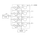
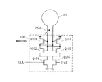
図6は、送電回路10の発振回路100が発生する信号の周波数および位相を調整するための構成の例を示すブロック図である。図6の構成では、基準クロック信号CLKを生成する基準クロック発生回路103と、送電回路10ごとに設けられ、クロック入力端子に入力された基準クロック信号CLKを遅延させ、遅延させたクロック信号を対応する送電回路10が備える発振回路100の同期制御入力端子に入力する可変遅延回路104(104−1〜104−4)とを追加している。
FIG. 6 is a block diagram illustrating an example of a configuration for adjusting the frequency and phase of a signal generated by the
各発振回路100(100−1〜100−4)は、同期制御入力端子を備えており、この同期制御入力端子に入力されるクロック信号に同期した信号を、送電コイル101(101−1〜101−4)とキャパシタ102(102−1〜102−4)とからなるLCタンク回路に出力する。発振回路100としては、バッファ、増幅回路、位相固定ループ(PLL:Phase-Locked Loop)回路、遅延固定ループ(DLL:Delay-Locked Loop)回路、インジェクションロック発振器(ILO:Injection-Locked Oscillator)などを用いても良い。
Each oscillation circuit 100 (100-1 to 100-4) includes a synchronization control input terminal, and a signal synchronized with a clock signal input to the synchronization control input terminal is transmitted to the power transmission coil 101 (101-1 to 101-101). -4) and the capacitor 102 (102-1 to 102-4). As the
発振回路100としてバッファを用いる場合、バッファは、同期制御入力端子に入力されるクロック信号を増幅してLCタンク回路に出力する。同様に、発振回路100として増幅回路を用いる場合、増幅回路は、同期制御入力端子に入力されるクロック信号を増幅してLCタンク回路に出力する。
When a buffer is used as the
発振回路100としてPLL回路またはDLL回路を用いる場合は、PLL回路またはDLL回路の参照クロック入力端子が発振回路100の同期制御入力端子となる。PLL回路またはDLL回路は、同期制御入力端子に入力されるクロック信号に同期した信号を生成してLCタンク回路に出力する。また、PLL回路またはDLL回路を用いる場合は、同期制御入力端子に入力されるクロック信号の周波数を逓倍してLCタンク回路に出力することも可能である。
When a PLL circuit or DLL circuit is used as the
発振回路100としてILOを用いる場合は、ILOのインジェクション入力端子が発振回路100の同期制御入力端子となる。ILOは、同期制御入力端子に入力されるクロック信号に同期した信号を生成してLCタンク回路に出力する。PLL回路またはDLL回路の場合と同様に、ILOを用いる場合も、同期制御入力端子に入力されるクロック信号の周波数を逓倍してLCタンク回路に出力することが可能である。
When an ILO is used as the
基準クロック発生回路103は、基準クロック信号CLKを生成する。この基準クロック信号CLKは、送電回路10ごとに設けられた可変遅延回路104(104−1〜104−4)によって遅延され、各送電回路10の発振回路100の同期制御入力端子に入力される。各発振回路100が送電コイル101とキャパシタ102とからなるLCタンク回路に出力する信号は、基準クロック発生回路103が発生した基準クロック信号CLKに同期したものとなる。
The reference
各発振回路100がLCタンク回路に出力する信号の周波数の調整を行う場合には、基準クロック発生回路103から出力する基準クロック信号CLKの周波数を調整するか、発振回路100の逓倍比を調整することで行う。また、周波数の調整を行う場合は、LCタンク回路の共振周波数も発振回路100の周波数と同じになるように調整することが望ましい。
When adjusting the frequency of the signal output from each
各発振回路100が出力する信号の位相は、可変遅延回路104(104−1〜104−4)の遅延量によって調整することができる。可変遅延回路104としては、電圧制御遅延ライン(VCDL:Voltage-Controlled Delay Line)、電流制御遅延ライン(CCDL:Current-Controlled Delay Line)、位相補間回路(PI:Phase Interpolator)、遅延段数選択回路、可変容量素子などを用いても良い。可変遅延回路104の遅延量の制御は、制御回路11から各可変遅延回路104に出力される位相制御信号によって行われる。こうして、図6に示した構成では、各発振回路100が出力する信号の位相を調整することができる。
The phase of the signal output from each
図7は、送電回路10の発振回路100が発生する信号の周波数および位相を調整するための構成の別の例を示すブロック図である。図7の構成では、基準クロック発生回路103を設けている。さらに、各送電回路10は、発振回路100の出力端子とLCタンク回路の入力端子との間に、発振回路100からクロック入力端子に入力された信号を遅延させ、遅延させた信号を後段のLCタンク回路に出力する可変遅延回路104(104−1〜104−4)を備えている。この図7に示す構成のように、発振回路100が発生する信号の位相を調整するための構成は、発振回路100と、送電コイル101とキャパシタ102とからなるLCタンク回路との間に可変遅延回路104を設け、発振回路100の出力を可変遅延回路104によって位相調整した後にLCタンク回路に出力するような構成でも良い。
FIG. 7 is a block diagram illustrating another example of a configuration for adjusting the frequency and phase of a signal generated by the
また、図8に示すように、送電回路10ごとに可変遅延回路104(104−1〜104−4)を設け、1つの発振回路100の出力端子と複数の可変遅延回路104のクロック入力端子とを接続し、1つの発振回路100を複数の送電回路10(10−1〜10−4)で共有するようにしてもよい。この場合は、発振回路100の出力を送電回路10ごとに設けた可変遅延回路104によって位相調整した後にLCタンク回路に出力することになる。
Further, as shown in FIG. 8, a variable delay circuit 104 (104-1 to 104-4) is provided for each
また、図9に示すように、発振回路100を、複数のインバータ等のゲート回路105を縦続接続したリング発振器と、複数のゲート回路105の出力信号のうちいずれか1つの信号を選択的に出力する選択回路106とから構成しても良い。
In addition, as shown in FIG. 9, the
選択回路106は、制御回路11から出力される位相制御信号に応じて、複数のゲート回路105の出力信号のうちいずれか1つの信号を選択して、送電コイル101とキャパシタ102とからなるLCタンク回路に出力する。こうして、図9に示したように発振回路100と可変遅延回路104とを一体化した構成で、発振回路100が出力する信号の位相を調整することができる。
The
図10は発振回路100としてILOを用いた場合の構成例を示す回路図である。図10の発振回路100は、ゲートが可変キャパシタ102aに接続され、ソースに電源電圧が供給され、ドレインが送電コイル101に接続されたPMOSトランジスタQ100と、ゲートが送電コイル101に接続され、ソースに電源電圧が供給され、ドレインが可変キャパシタ102aに接続されたPMOSトランジスタQ101と、ゲートが可変キャパシタ102aに接続され、ドレインがPMOSトランジスタQ100のドレインに接続されたNMOSトランジスタQ102と、ゲートが送電コイル101に接続され、ドレインがPMOSトランジスタQ101のドレインに接続されたNMOSトランジスタQ103と、同期制御入力端子となるゲートに基準クロック発生回路103から可変遅延回路104を経由して入力されるクロック信号CLKが供給され、ドレインがNMOSトランジスタQ102,Q103のソースに接続され、ソースが接地されたNMOSトランジスタQ104と、ゲートに基準電圧Vrefが供給され、ドレインがNMOSトランジスタQ102,Q103のソースに接続され、ソースが接地されたNMOSトランジスタQ105とから構成される。
FIG. 10 is a circuit diagram showing a configuration example when an ILO is used as the
図10に示した回路では、送電回路10のLCタンク回路が発振回路100の一部を形成している。この発振回路100の発振周波数は基本的に送電回路10のLCタンク回路の共振周波数で決まる。そこで、図10の回路では、送電コイル101と可変キャパシタ102aとからLCタンク回路を構成する。この可変キャパシタ102aによって発振回路100の発振周波数の微調整を行うことができる。可変キャパシタ102aの例としては、バラクタ素子がある。
In the circuit shown in FIG. 10, the LC tank circuit of the
また、発振回路100の発振周波数の微調整および発振位相の制御は、可変遅延回路104から発振回路100の同期制御入力端子(NMOSトランジスタQ104のゲート)に入力されるクロック信号CLKによっても行うことができる。発振回路100は、この同期制御入力端子に入力されるクロック信号CLKに同期するように発振位相を補正する。
The fine adjustment of the oscillation frequency of the
図11は発振回路100としてILOを用いた場合の別の構成例を示す回路図である。図11の発振回路100は、ゲートが可変キャパシタ102aに接続され、ソースに電源電圧が供給され、ドレインが送電コイル101に接続されたPMOSトランジスタQ106と、ゲートが送電コイル101に接続され、ソースに電源電圧が供給され、ドレインが可変キャパシタ102aに接続されたPMOSトランジスタQ107と、ゲートが可変キャパシタ102aに接続され、ドレインがPMOSトランジスタQ106のドレインに接続され、ソースが接地されたNMOSトランジスタQ108と、ゲートが送電コイル101に接続され、ドレインがPMOSトランジスタQ107のドレインに接続され、ソースが接地されたNMOSトランジスタQ109と、同期制御入力端子となるゲートに基準クロック発生回路103から可変遅延回路104を経由して入力されるクロック信号CLKが供給され、ドレインがPMOSトランジスタQ106のドレインおよびNMOSトランジスタQ108のドレインに接続され、ソースがPMOSトランジスタQ107のドレインおよびNMOSトランジスタQ109のドレインに接続されたNMOSトランジスタQ110とから構成される。
FIG. 11 is a circuit diagram showing another configuration example when an ILO is used as the
図12は送電回路10の発振回路100が発生する信号の周波数および位相を調整するための構成の別の例を示すブロック図であり、複数の基準クロックを用いる場合の構成例を示すブロック図である。図4、図5を用いて説明したように、特定の送電コイル101と受電コイル200との間で電力伝送チャネルを形成して、他の受電コイル200への電力伝送を遮断するために、発振周波数によるチャネル選択を行う場合がある。このような場合、図12に示すように基準クロック発生回路から出力される複数の基準クロック信号CLK1,CLK2,CLK3を用いることで、周波数空間でのチャネル選択を行うことが可能になる。基準クロック信号CLK1,CLK2,CLK3は、それぞれ異なる周波数の信号である。
FIG. 12 is a block diagram illustrating another example of a configuration for adjusting the frequency and phase of a signal generated by the
図12の例では、発振周波数の選択を行うために、複数のスイッチ素子107をマトリクス状に配置したスイッチアレイ108を用いている。スイッチアレイ108のスイッチ素子107をオン/オフすることにより、各可変遅延回路104(104−1〜104−4)に基準クロック信号CLK1,CLK2,CLK3のうちいずれか1つのクロック信号を任意に入力することができる。こうして、各発振回路100(100−1〜100−4)の発振周波数を選択することができる。スイッチ素子107のオン/オフは、制御回路11によって制御される。
In the example of FIG. 12, a switch array 108 in which a plurality of switch elements 107 are arranged in a matrix is used to select an oscillation frequency. By turning on / off the switch element 107 of the switch array 108, any one of the reference clock signals CLK1, CLK2, and CLK3 is arbitrarily input to each variable delay circuit 104 (104-1 to 104-4). can do. Thus, the oscillation frequency of each oscillation circuit 100 (100-1 to 100-4) can be selected. On / off of the switch element 107 is controlled by the
なお、図7、図8において、発振回路100の前段にスイッチアレイを設け、発振回路100に入力する基準クロック信号をスイッチアレイで任意に切り替える構成としてもよい。
7 and 8, a switch array may be provided in front of the
また、本実施の形態において、発振回路100の発振周波数の調整は、図12に示したような方式以外にも、前記のとおり、発振回路100でクロック信号の周波数の逓倍比を変えることでも可能になる。基準クロック発生回路103および発振回路100が生成する信号の周波数を微調整するには、分数分周(Fractional-N)方式のPLL回路を用いれば良い。分数分周方式のPLL回路を用いることで、精度良く細かなステップでの周波数調整が可能になる。
In the present embodiment, the oscillation frequency of the
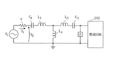
図13は送電回路10に電流検出回路と電圧検出回路を付加した構成を示すブロック図である。図13におけるV1は発振回路100が生成する電圧、rは寄生抵抗である。発振回路100からLCタンク回路に流れる電流I1を検出する電流検出回路109と発振回路100からLCタンク回路に印加される電圧V2を検出する電圧検出回路110を付加することにより、送電回路10の送電コイル101と受電回路20の受電コイル200との間の結合係数kの変化や、受電回路20の負荷インピーダンスZの変化を検出することが可能になる。
FIG. 13 is a block diagram showing a configuration in which a current detection circuit and a voltage detection circuit are added to the
図14は図13の送電回路10と受電回路20の等価回路図である。図14では、図13の送電回路10の送電コイル101の一端と受電回路20の受電コイル200の一端とを接地と見なしている。ここでは、送電コイル101のインダクタンスをL1、受電コイル200のインダクタンスをL2、キャパシタ102の値をC1、キャパシタ201の値をC2としている。インダクタL3,L5のインダクタンスはL1−k(L1L2)1/2、インダクタL4のインダクタンスはk(L1L2)1/2である。
FIG. 14 is an equivalent circuit diagram of the
図14に示した回路図から、結合係数kが変化した場合や、負荷インピーダンスZが変化した場合に、インダクタL3より右側の回路のインピーダンスが変化し、その結果として送電回路10内で電流I1が変化するか、またはLCタンク回路に印加される電圧V2が変化することが分かる。
From the circuit diagram shown in FIG. 14, when the coupling coefficient k changes or when the load impedance Z changes, the impedance of the circuit on the right side of the inductor L 3 changes, and as a result, the current I in the
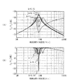
図15(A)、図15(B)は図14の回路において結合係数kを変化させた場合のスパイス(Spice)シミュレーションの結果を示す図であり、図15(A)は結合係数kと発振回路100の周波数の変化に対する送電回路10のI1/V1の変化を示す図、図15(B)は結合係数kと発振回路100の周波数の変化に対する送電回路10のV2/V1の変化を示す図である。図15(A)、図15(B)に示した結果から、送電回路10内の発振回路100からLCタンク回路に流れる電流I1または発振回路100からLCタンク回路に印加される電圧V2を測定することで、結合係数kの変化や負荷インピーダンスZの変化を読み取ることが可能であることが分かる。
15A and 15B are diagrams showing the results of a spice simulation when the coupling coefficient k is changed in the circuit of FIG. 14, and FIG. 15A shows the coupling coefficient k and oscillation. It shows the change in I 1 / V 1 of the
複数ある送電回路10の送電コイル101と受電回路20の受電コイル200との距離はそれぞれ異なるので、結合係数kも異なる。前述の送電回路10内部での電流I1または電圧V2の測定結果を用いることで、受電コイル200との結合係数kが高い送電コイル101を探索することが可能であり、結合係数kが最も高い送電コイル101が受電回路20に最も近いと推測することができる。
Since the distance between the
例えば電流I1の場合、図15(A)に示すように、結合係数kによって極大値や極小値が現れる周波数が異なり、また極大値や極小値の大きさが異なるので、これら極大値や極小値の情報から結合係数kの値を推測することができる。また、電圧V2の場合、図15(B)に示すように、結合係数kによって極小値が現れる周波数が異なり、また極小値の大きさが異なるので、極小値の情報から結合係数kの値を推測することができる。 For example, in the case of the current I 1 , as shown in FIG. 15A, the frequency at which the maximum value and the minimum value appear varies depending on the coupling coefficient k, and the maximum value and the minimum value differ. The value of the coupling coefficient k can be estimated from the value information. In the case of the voltage V 2 , as shown in FIG. 15B, the frequency at which the minimum value appears varies depending on the coupling coefficient k, and the magnitude of the minimum value varies. Can be guessed.
このように、送電回路10ごとに内部の電流I1または電圧V2を測定する。非接触送電装置1の制御回路11は、各送電回路10の測定結果を比較することで、受電コイル200との結合係数kが最も高い送電コイル101を探索することができるので、受電回路20に最も近い送電回路10を探索することができ、結果として受電回路20の位置を特定することが可能である。また、制御回路11は、結合係数kの値から、送電回路10の送電コイル101と受電回路20の受電コイル200との距離も推定することが可能である。
Thus, the internal current I 1 or voltage V 2 is measured for each
なお、送電コイル101と受電コイル200との距離の推定のためには、結合係数kと距離とを対応付けて記憶するテーブルもしくは結合係数kから距離を算出する数式を、制御回路11の内部にあらかじめ設定しておけばよい。制御回路11は、内部に設定されたテーブルもしくは数式を用いることにより、推定した結合係数kから距離を求めることができる。
In order to estimate the distance between the
以上のような受電回路20の位置の特定、距離の推定などの特徴は、従来のフェイズドアレイアンテナを用いた電波の送受信には無い特徴であり、インダクタ結合を用いた回路特有のものである。
The characteristics such as the specification of the position of the
非接触送電装置1の制御回路11は、受電回路20の位置の特定結果、送電回路10の送電コイル101と受電回路20の受電コイル200との距離の推定結果を用いて、アレイ状に並べられた複数の送電回路10の中からどの送電回路10を送電に用いるかを選択したり、各送電回路10の発振回路100が生成する信号の位相を調整したりする。前述のとおり、送電回路10のオン/オフ制御は、制御回路11から各送電回路10に出力される発振オン/オフ制御信号によって行われる。また、発振位相の制御は、制御回路11から各送電回路10に出力される位相制御信号によって行われる。
The
動作させる送電回路10は、図3を用いて説明したように、受電回路20の受電コイル200に近いものから優先的に用いることが好ましい。各送電回路10の発振回路100が生成する信号間の位相差は、結合係数kから各送電回路10と受電回路20間の距離を概算して、これらの距離の差を各送電回路10間について求めたときに、この距離の差を、電磁波の進行速度(空気中では大凡3×10⁸m/s)で割った時間を位相に換算したものを用いることが好ましい。
As described with reference to FIG. 3, the
また、図15に示したように発振回路100の周波数によって送電回路10の電流I1、電圧V2の測定値が大きく変わるので、制御回路11は、発振回路100の発振周波数の調整を行う場合、発振回路100の周波数を掃引して、送電回路10内の電流I1が最大になる周波数、または電圧V2が最小になる周波数を選んでも良い。前述のとおり、発振周波数の制御は、制御回路11から各送電回路10に出力される周波数制御信号によって行われる。
Further, as shown in FIG. 15, the measured values of the current I 1 and the voltage V 2 of the
各送電回路10の送電コイル101と受電回路20の受電コイル200との間の結合係数kなどを測定する場合には、送電回路10を1つずつ順番に動作さることで、他の送電回路10の影響を排除した、特定の送電回路10の送電コイル101と受電回路20の受電コイル200との関係の純粋な測定結果を得られ易い。
When measuring the coupling coefficient k or the like between the
したがって、制御回路11は、送電回路10を1つずつシーケンシャルに動作させて結合係数k、受電回路20の位置、送電回路10の送電コイル101と受電回路20の受電コイル200との距離などの情報を収集した後に、各送電回路10の発振のオン/オフ、位相の調整、周波数の調整を行うことが望ましい。複数の送電回路10の発振回路100を同時に動作させると、このような情報を精度良く収集することが難しくなる。
Therefore, the
受電回路20への送電に用いる送電回路10の選択や発振回路100が発生する信号の位相の決定などのキャリブレーションは、受電回路20からのフィードバック情報を用いて行っても良い。図16は受電回路20からのフィードバック情報を用いて送電回路10を制御する場合の構成例を示すブロック図である。
Calibration such as selection of the
受電回路20の受信電力強度検出回路204は、受信電力の強度を検出する。そして、受信電力強度検出回路204は、受信電力の強度の検出結果を符号化してデジタル信号に変換するか、検出結果を振幅、周波数、パルス幅、位相などの物理量で示すアナログ信号に変換して、このデジタル信号またはアナログ信号で負荷インピーダンス可変回路205を制御し、受信電力が最大になるように受電回路20の負荷インピーダンスZを変化させる。このとき、非接触送電装置1側では、前述のとおり結合係数kの測定結果から、発振回路100のオン/オフ、発振周波数、発振の位相、発振信号の振幅のうち少なくとも1つを制御すれば良い。受電回路20の負荷インピーダンスZを変化させる負荷インピーダンス可変回路205は、例えばトランジスタやバラクタ素子によって実現することができる。
The received power
また、受電回路20の受信電力強度検出回路204は、検出した受信電力の強度の情報を非接触送電装置1に無線送信するようにしても良い。この場合、非接触送電装置1には、受電回路20から送信された情報を受信する受信手段(不図示)を設ける。非接触送電装置1の制御回路11は、受信電力強度検出回路204から受信した情報に基づいて、受電回路20の受信電力が最大になるように、各送電回路10の発振回路100のオン/オフ、発振周波数、発振の位相、発振信号の振幅のうち少なくとも1つを制御すれば良い。このときの制御回路11による制御の手法は、結合係数kの測定結果を用いて制御する場合と同様である。
Further, the received power
また、送電回路10内の電流検出回路109、または電圧検出回路110を用いれば、受電回路20が非接触送電装置1から遠ざかったことを検出することも可能である。この場合、結合係数kは零になる。そこで、非接触送電装置1の制御回路11は、結合係数kが零になったとき、もしくは結合係数kが所定の閾値より低下したときに、受電回路20が所定の許容範囲外に移動したと判断して、各送電回路10の発振回路100の動作を停止させるか、あるいは発振回路100の出力電力を低下させる。こうして、本実施の形態では、受電回路20が非接触送電装置1から遠ざかったときに、無駄な電力消費を抑制することができる。
Further, if the
ただし、発振回路100を完全に停止させると、受電回路20が送電回路10の近傍に現われた場合でも受電回路20の検出ができなくなる。そこで、制御回路11は、各送電回路10の発振回路100から微弱な信号を、送電コイル101とキャパシタ102とからなるLCタンク回路に出力させるか、あるいは発振回路100から間欠的に信号をLCタンク回路に出力させて、このときの電流検出回路109または電圧検出回路110の測定結果から、受電回路20の接近を検出することが望ましい。例えば制御回路11は、結合係数kが零より大きくなったとき、もしくは結合係数kが所定の閾値より大きくなったときに、受電回路20が接近したと判断する。
However, if the
制御回路11は、受電回路20の接近を検出した後に、前述のとおり、動作させる発振回路100の選択、発振周波数の調整、発振位相の調整、発振信号の振幅の調整などのキャリブレーションや、受電回路20との間で送信電力の大きさの調整などのネゴシエーションを行い、必要があれば受電回路20に電力の送信を行う。
After detecting the approach of the
本実施の形態の非接触送電装置1の制御回路11は、例えばCPU、記憶装置およびインタフェースを備えたコンピュータと、これらのハードウェア資源を制御するプログラムによって実現することができる。CPUは、記憶装置に格納されたプログラムに従って本実施の形態で説明した処理を実行する。
The
上記の実施の形態の一部又は全部は、以下の付記のようにも記載されうるが、以下には限られない。 A part or all of the above embodiments can be described as in the following supplementary notes, but is not limited thereto.
(付記1)N(Nは2以上の整数)個の送電回路と、このN個の送電回路を制御する制御手段とを備え、前記送電回路は、直列に接続されたキャパシタと送電コイルとからなる送電側LCタンク回路と、この送電側LCタンク回路に電力を供給する発振回路とを有し、前記N個の送電回路の送電コイルは、マトリクス状に配置され、前記制御手段は、前記N個の送電回路の送電コイルのうち少なくとも2個の送電コイルから到達する磁場の変化の位相が受電回路の受電コイルにおいて揃うように、前記N個の送電回路の各発振回路が発生する信号の位相を制御することを特徴とする非接触送電装置。 (Supplementary note 1) It is provided with N (N is an integer of 2 or more) power transmission circuits and control means for controlling the N power transmission circuits. The power transmission circuit includes a capacitor and a power transmission coil connected in series. A power transmission side LC tank circuit and an oscillation circuit for supplying power to the power transmission side LC tank circuit. The power transmission coils of the N power transmission circuits are arranged in a matrix, and the control means includes the N Phases of signals generated by the oscillation circuits of the N power transmission circuits so that the phases of changes in the magnetic field reaching from at least two power transmission coils of the power transmission coils of the power transmission circuits are aligned in the power reception coils of the power reception circuits. A non-contact power transmission device characterized by controlling the power.
(付記2)付記1記載の非接触送電装置において、前記制御手段は、さらに、前記N個の送電回路の各発振回路のオン/オフ、発振周波数、発振信号の振幅のうち少なくとも1つを制御することを特徴とする非接触送電装置。
(Supplementary note 2) In the non-contact power transmission device according to
(付記3)付記2記載の非接触送電装置において、前記制御手段は、前記N個の送電回路のうちM(MはN以下の整数)個の送電回路の発振回路を同じ周波数で発振させ、このM個の送電回路に含まれる第1の送電回路の発振回路が発生する信号と前記M個の送電回路に含まれる第2の送電回路の発振回路が発生する信号との位相差が、前記第1の送電回路の送電コイルと前記受電回路の受電コイルとの間の距離と、前記第2の送電回路の送電コイルと前記受電コイルとの間の距離との差に比例するように、前記M個の送電回路の各発振回路が発生する信号の位相を制御することを特徴とする非接触送電装置。
(Supplementary note 3) In the non-contact power transmission device according to
(付記4)付記2記載の非接触送電装置において、前記制御手段は、R(RはN以下の整数)個の前記受電回路の各々に対応して少なくとも2個の送電回路を受電回路ごとに動作させ、各送電回路が備える発振回路を、対応する受電回路ごとに異なる周波数で発振させることを特徴とする非接触送電装置。
(Supplementary note 4) In the non-contact power transmission device according to
(付記5)付記1乃至付記4のいずれか1つに記載の非接触送電装置において、さらに、基準クロック信号を生成する基準クロック信号発生回路と、前記送電回路ごとに設けられ、クロック入力端子に入力された前記基準クロック信号を遅延させ、遅延させたクロック信号を対応する送電回路が備える発振回路の同期制御入力端子に入力するN個の可変遅延回路とを備え、前記制御手段は、N個の位相制御信号を前記N個の可変遅延回路の制御入力端子に入力し、前記N個の可変遅延回路の遅延量を制御することにより、前記N個の送電回路の各発振回路が発生する信号の位相を制御することを特徴とする非接触送電装置。
(Supplementary note 5) In the non-contact power transmission device according to any one of
(付記6)付記1乃至付記4のいずれか1つに記載の非接触送電装置において、さらに、基準クロック信号を前記N個の送電回路が備える発振回路の同期制御入力端子に入力する基準クロック信号発生回路を備え、前記N個の送電回路は、前記発振回路の出力端子と前記送電側LCタンク回路の入力端子との間に、前記発振回路からクロック入力端子に入力された信号を遅延させ、遅延させた信号を後段の送電側LCタンク回路に入力する可変遅延回路をそれぞれ備え、前記制御手段は、N個の位相制御信号をN個の前記可変遅延回路の制御入力端子に入力し、前記N個の可変遅延回路の遅延量を制御することにより、前記N個の送電回路の各発振回路が発生する信号の位相を制御することを特徴とする非接触送電装置。
(Supplementary note 6) In the contactless power transmission device according to any one of
(付記7)付記1乃至付記6のいずれか1項に記載の非接触送電装置において、前記N個の送電回路は、前記発振回路から前記送電側LCタンク回路に流れる電流と前記発振回路から前記送電側LCタンク回路に印加される電圧のうち少なくとも一方を検出する検出回路をそれぞれ備え、前記制御手段は、前記検出回路の検出結果に基づいて、少なくとも前記N個の送電回路の各発振回路が発生する信号の位相を制御することを特徴とする非接触送電装置。
(Supplementary note 7) In the non-contact power transmission device according to any one of
(付記8)付記7記載の非接触送電装置と、この非接触送電装置から電力供給を受ける受電回路とを備え、前記受電回路は、直列に接続されたキャパシタと受電コイルとからなる受電側LCタンク回路と、この受電側LCタンク回路に接続される負荷インピーダンスを変化させる負荷インピーダンス可変回路と、前記受電側LCタンク回路の出力に基づいて受信電力の強度を検出し、受信電力が最大になるように前記負荷インピーダンスを変化させる受信電力強度検出手段とを備えることを特徴とする非接触送電システム。 (Additional remark 8) It is provided with the non-contact power transmission apparatus of Additional remark 7, and the power receiving circuit which receives electric power supply from this non-contact power transmission apparatus, The said power receiving circuit is the power receiving side LC which consists of the capacitor and receiving coil which were connected in series Based on the output of the tank circuit, the load impedance variable circuit for changing the load impedance connected to the power receiving side LC tank circuit, and the output of the power receiving side LC tank circuit, the received power intensity is maximized. A non-contact power transmission system comprising: received power intensity detecting means for changing the load impedance as described above.
(付記9)付記7記載の非接触送電装置と、この非接触送電装置から電力供給を受ける受電回路とを備え、前記受電回路は、直列に接続されたキャパシタと受電コイルとからなる受電側LCタンク回路と、この受電側LCタンク回路の出力に基づいて受信電力の強度を検出し、検出した受信電力の強度の情報を前記非接触送電装置に無線送信する受信電力強度検出手段とを備え、前記送電回路は、前記受電回路から送信された情報を受信する受信手段を備え、前記制御手段は、前記受電回路から送信された情報に基づいて、前記受電回路の受信電力が最大になるように、少なくとも前記N個の送電回路の各発振回路が発生する信号の位相を制御することを特徴とする非接触送電システム。 (Additional remark 9) It is provided with the non-contact power transmission apparatus of Additional remark 7, and the power receiving circuit which receives electric power supply from this non-contact power transmission apparatus, The said power receiving circuit is the power receiving side LC which consists of the capacitor and receiving coil which were connected in series A tank circuit; and a received power intensity detecting means for detecting the intensity of the received power based on the output of the power receiving side LC tank circuit, and wirelessly transmitting information on the detected received power intensity to the non-contact power transmission device, The power transmission circuit includes reception means for receiving information transmitted from the power reception circuit, and the control means is configured to maximize the received power of the power reception circuit based on the information transmitted from the power reception circuit. A contactless power transmission system that controls a phase of a signal generated by each oscillation circuit of at least the N power transmission circuits.
(付記10)直列に接続されたキャパシタと送電コイルとからなる送電側LCタンク回路と、この送電側LCタンク回路に電力を供給する発振回路とをそれぞれ備えたN(Nは2以上の整数)個の送電回路を用いて、受電回路への電力供給を行う非接触送電方法において、前記N個の送電回路の送電コイルは、マトリクス状に配置され、前記N個の送電回路の送電コイルのうち少なくとも2個の送電コイルから到達する磁場の変化の位相が前記受電回路の受電コイルにおいて揃うように、前記N個の送電回路の各発振回路が発生する信号の位相を制御することを特徴とする非接触送電方法。 (Additional remark 10) N (N is an integer greater than or equal to 2) each provided with the power transmission side LC tank circuit which consists of the capacitor and power transmission coil which were connected in series, and the oscillation circuit which supplies electric power to this power transmission side LC tank circuit In the non-contact power transmission method for supplying power to the power receiving circuit using the number of power transmission circuits, the power transmission coils of the N power transmission circuits are arranged in a matrix, and among the power transmission coils of the N power transmission circuits The phase of the signal generated by each oscillation circuit of the N power transmission circuits is controlled so that the phase of the change in the magnetic field arriving from at least two power transmission coils is aligned in the power reception coil of the power reception circuit. Non-contact power transmission method.
(付記11)付記1記載の非接触送電装置において、各発振回路は、他の送電回路の発振回路と同期して発振することが可能であることを特徴とする非接触送電装置。
(Supplementary note 11) The non-contact power transmission device according to
(付記12)付記1記載の非接触送電装置において、前記制御手段は、前記N個の送電回路のうち、前記受電回路の受電コイルとの距離が近い順にM番目(MはN以下の整数)までの送電回路を選択し、このM個の送電回路が備える発振回路を同じ周波数で発振させることを特徴とする非接触送電装置。
(Additional remark 12) In the non-contact power transmission device according to
(付記13)付記5または付記6記載の非接触送電装置において、前記可変遅延回路は、電圧制御型遅延素子、電流制御型遅延素子、位相補間回路、遅延素子の段数を切り替える遅延段数選択回路、可変容量素子、多相クロック信号から任意の位相を選択するセレクタ回路、の何れかからなることを特徴とする非接触送電装置。
(Supplementary note 13) In the non-contact power transmission device according to
(付記14)付記1記載の非接触送電装置において、前記送電回路が備える発振回路は、同期制御入力端子に入力されたクロック信号を増幅するバッファ回路、同期制御入力端子に入力されたクロック信号を増幅する増幅回路、同期制御入力端子に入力されたクロック信号に同期した信号を生成する位相ロックループ回路、同期制御入力端子に入力されたクロック信号に同期した信号を生成する遅延ロックループ回路、同期制御入力端子に入力されたクロック信号に同期した信号を生成するインジェクションロック発振回路、の何れかからなることを特徴とする非接触送電装置。
(Supplementary note 14) In the non-contact power transmission device according to
(付記15)付記1記載の非接触送電装置において、前記送電回路が備えるキャパシタは、その容量値が外部からの制御信号によって可変であるバラクタ素子であることを特徴とすることを特徴とする非接触送電装置。
(Supplementary note 15) In the non-contact power transmission device according to
(付記16)付記15記載の非接触送電装置において、前記送電回路が備える発振回路が生成する信号の周波数を変更するとき、または基準クロック信号の周波数を変更するときに、前記バラクタ素子によって前記送電回路のキャパシタの容量値を調整することを特徴とすることを特徴とする非接触送電装置。
(Supplementary note 16) In the non-contact power transmission device according to
(付記17)付記1記載の非接触送電装置において、さらに、周波数が異なる複数のクロック信号のうち任意の基準クロック信号を、前記送電回路が備える発振回路の同期制御入力端子、または前記可変遅延回路のクロック入力端子に選択的に入力するスイッチ素子を備えることを特徴とする非接触送電装置。
(Supplementary note 17) In the non-contact power transmission device according to
(付記18)付記1記載の非接触送電装置において、前記送電回路が備える発振回路は、同期制御入力端子に入力されたクロック信号の周波数を逓倍した周波数の信号を出力することを特徴とする非接触送電装置。
(Supplementary note 18) In the non-contact power transmission device according to
(付記19)付記7記載の非接触送電装置において、前記制御手段は、前記検出回路の検出結果に基づいて前記受電回路の受電コイルに近い送電回路を検出し、受電コイルに近い少なくとも2個の送電回路の発振回路を動作させることを特徴とする非接触送電装置。 (Supplementary note 19) In the non-contact power transmission device according to supplementary note 7, the control unit detects a power transmission circuit close to the power reception coil of the power reception circuit based on a detection result of the detection circuit, and includes at least two power transmission coils close to the power reception coil A non-contact power transmission device that operates an oscillation circuit of a power transmission circuit.
(付記20)付記1記載の非接触送電装置において、前記制御手段は、前記送電回路の送電コイルと前記受電回路の受電コイルとの距離が近い場合には少数の前記送電回路を動作させ、前記送電回路の送電コイルと前記受電回路の受電コイルとの距離が遠くなるに従い動作させる前記送電回路の数を増やす制御を行うことを特徴とする非接触送電装置。
(Supplementary note 20) In the non-contact power transmission device according to
(付記21)付記19記載の非接触送電装置において、前記制御手段は、前記検出回路の検出結果から、前記送電回路の送電コイルと前記受電回路の受電コイルとの距離を求めることを特徴とする非接触送電装置。 (Supplementary note 21) In the non-contact power transmission device according to supplementary note 19, the control unit obtains a distance between a power transmission coil of the power transmission circuit and a power reception coil of the power reception circuit from a detection result of the detection circuit. Non-contact power transmission device.
(付記22)付記8記載の非接触送電システムにおいて、前記負荷インピーダンス可変回路は、トランジスタ、バラクタ素子の何れかを含むことを特徴とする非接触送電システム。 (Supplementary note 22) The non-contact power transmission system according to supplementary note 8, wherein the load impedance variable circuit includes either a transistor or a varactor element.
(付記23)付記7記載の非接触送電装置において、前記制御手段は、前記検出回路の検出結果に基づいて、前記受電回路が許容範囲外に遠ざかったことを検出したときに、前記送電回路が備える発振回路の動作を停止させるか、前記送電回路が備える発振回路の出力電力を低下させることを特徴とする非接触送電装置。 (Supplementary note 23) In the non-contact power transmission device according to supplementary note 7, when the control unit detects that the power reception circuit has moved away from an allowable range based on a detection result of the detection circuit, A non-contact power transmission apparatus that stops an operation of an oscillation circuit provided or reduces output power of an oscillation circuit provided in the power transmission circuit.
(付記24)付記7記載の非接触送電装置において、前記制御手段は、送電を行っていない送電回路または発振回路が停止している送電回路において、発振回路を間欠的に動作させ、その動作中に前記検出回路を用いて前記受電回路の接近を検出することを特徴とする非接触送電装置。 (Supplementary note 24) In the non-contact power transmission device according to supplementary note 7, the control means operates the oscillation circuit intermittently in a power transmission circuit that is not performing power transmission or a power transmission circuit in which the oscillation circuit is stopped. A contactless power transmission device that detects an approach of the power receiving circuit using the detection circuit.
(付記25)付記24記載の非接触送電装置において、前記制御手段は、前記発振回路を間欠的に動作させる際に、前記N個の送電回路が備える発振回路を1つずつ順次動作させることを特徴とする非接触送電装置。 (Supplementary note 25) In the non-contact power transmission device according to supplementary note 24, the control unit sequentially operates the oscillation circuits included in the N power transmission circuits one by one when the oscillation circuit is intermittently operated. A contactless power transmission device.
本実施の形態は、受電回路への電力供給を電磁共鳴を用いて非接触で行う技術に適用することができる。 This embodiment can be applied to a technique in which power is supplied to a power receiving circuit in a contactless manner using electromagnetic resonance.
1…非接触送電装置、10,10−1〜10−6…送電回路、11…制御回路、20,20−1〜20−3…受電回路、100,100−1〜100−6…発振回路、101,101−1〜101−6…送電コイル、102,102−1〜102−6…キャパシタ、102a…可変キャパシタ、103…基準クロック発生回路、104−1〜104−4…可変遅延回路、105…ゲート回路、106…選択回路、107…スイッチ素子、108…スイッチアレイ、109…電流検出回路、110…電圧検出回路、200,200−1〜200−3…受電コイル、201,201−1〜201−3…キャパシタ、202,202−1〜202−3…整流回路、203,203−1〜203−3…負荷、204…受信電力強度検出回路、205…負荷インピーダンス可変回路、Q100〜Q110…トランジスタ。
DESCRIPTION OF
Claims (10)
前記送電回路は、
直列に接続されたキャパシタと送電コイルとからなる送電側LCタンク回路と、
この送電側LCタンク回路に電力を供給する発振回路とを有し、
前記N個の送電回路の送電コイルは、マトリクス状に配置され、
前記制御手段は、前記N個の送電回路の送電コイルのうち少なくとも2個の送電コイルから到達する磁場の変化の位相が受電回路の受電コイルにおいて揃うように、前記N個の送電回路の各発振回路が発生する信号の位相を制御することを特徴とする非接触送電装置。 N (N is an integer of 2 or more) power transmission circuits, and control means for controlling the N power transmission circuits,
The power transmission circuit is:
A power transmission side LC tank circuit composed of a capacitor and a power transmission coil connected in series;
An oscillation circuit for supplying power to the power transmission side LC tank circuit,
The power transmission coils of the N power transmission circuits are arranged in a matrix,
The control means is configured to control each oscillation of the N power transmission circuits so that the phase of the change in the magnetic field reaching from at least two power transmission coils among the power transmission coils of the N power transmission circuits is aligned in the power reception coils of the power reception circuit. A non-contact power transmission device that controls a phase of a signal generated by a circuit.
前記制御手段は、さらに、前記N個の送電回路の各発振回路のオン/オフ、発振周波数、発振信号の振幅のうち少なくとも1つを制御することを特徴とする非接触送電装置。 The contactless power transmission device according to claim 1,
The contactless power transmission device, wherein the control means further controls at least one of on / off of each oscillation circuit of the N power transmission circuits, an oscillation frequency, and an amplitude of an oscillation signal.
前記制御手段は、前記N個の送電回路のうちM(MはN以下の整数)個の送電回路の発振回路を同じ周波数で発振させ、このM個の送電回路に含まれる第1の送電回路の発振回路が発生する信号と前記M個の送電回路に含まれる第2の送電回路の発振回路が発生する信号との位相差が、前記第1の送電回路の送電コイルと前記受電回路の受電コイルとの間の距離と、前記第2の送電回路の送電コイルと前記受電コイルとの間の距離との差に比例するように、前記M個の送電回路の各発振回路が発生する信号の位相を制御することを特徴とする非接触送電装置。 The contactless power transmission device according to claim 2,
The control means oscillates oscillation circuits of M (M is an integer equal to or less than N) power transmission circuits among the N power transmission circuits at the same frequency, and a first power transmission circuit included in the M power transmission circuits The phase difference between the signal generated by the oscillation circuit of the first power transmission circuit and the signal generated by the oscillation circuit of the second power transmission circuit included in the M power transmission circuits is the power reception of the power transmission coil of the first power transmission circuit and the power reception circuit. Of the signals generated by the oscillation circuits of the M power transmission circuits so as to be proportional to the difference between the distance between the coils and the distance between the power transmission coil of the second power transmission circuit and the power reception coil. A contactless power transmission device that controls a phase.
前記制御手段は、R(RはN以下の整数)個の前記受電回路の各々に対応して少なくとも2個の送電回路を受電回路ごとに動作させ、各送電回路が備える発振回路を、対応する受電回路ごとに異なる周波数で発振させることを特徴とする非接触送電装置。 The contactless power transmission device according to claim 2,
The control means operates at least two power transmission circuits corresponding to each of R (R is an integer equal to or less than N) power reception circuits for each power reception circuit, and corresponds to an oscillation circuit included in each power transmission circuit. A non-contact power transmission device that oscillates at a different frequency for each power receiving circuit.
さらに、基準クロック信号を生成する基準クロック信号発生回路と、
前記送電回路ごとに設けられ、クロック入力端子に入力された前記基準クロック信号を遅延させ、遅延させたクロック信号を対応する送電回路が備える発振回路の同期制御入力端子に入力するN個の可変遅延回路とを備え、
前記制御手段は、N個の位相制御信号を前記N個の可変遅延回路の制御入力端子に入力し、前記N個の可変遅延回路の遅延量を制御することにより、前記N個の送電回路の各発振回路が発生する信号の位相を制御することを特徴とする非接触送電装置。 In the non-contact power transmission device according to any one of claims 1 to 4,
A reference clock signal generation circuit for generating a reference clock signal;
N variable delays provided for each power transmission circuit, delaying the reference clock signal input to the clock input terminal, and inputting the delayed clock signal to the synchronization control input terminal of the oscillation circuit included in the corresponding power transmission circuit With circuit,
The control means inputs N phase control signals to the control input terminals of the N variable delay circuits, and controls the delay amount of the N variable delay circuits, thereby controlling the N power transmission circuits. A non-contact power transmission apparatus that controls a phase of a signal generated by each oscillation circuit.
さらに、基準クロック信号を前記N個の送電回路が備える発振回路の同期制御入力端子に入力する基準クロック信号発生回路を備え、
前記N個の送電回路は、前記発振回路の出力端子と前記送電側LCタンク回路の入力端子との間に、前記発振回路からクロック入力端子に入力された信号を遅延させ、遅延させた信号を後段の送電側LCタンク回路に入力する可変遅延回路をそれぞれ備え、
前記制御手段は、N個の位相制御信号をN個の前記可変遅延回路の制御入力端子に入力し、前記N個の可変遅延回路の遅延量を制御することにより、前記N個の送電回路の各発振回路が発生する信号の位相を制御することを特徴とする非接触送電装置。 In the non-contact power transmission device according to any one of claims 1 to 4,
And a reference clock signal generation circuit for inputting a reference clock signal to a synchronization control input terminal of an oscillation circuit included in the N power transmission circuits.
The N power transmission circuits delay a signal input from the oscillation circuit to the clock input terminal between the output terminal of the oscillation circuit and the input terminal of the power transmission side LC tank circuit, and the delayed signal Each is provided with a variable delay circuit that inputs to the power transmission side LC tank circuit at the subsequent stage,
The control means inputs N phase control signals to control input terminals of the N variable delay circuits, and controls the delay amount of the N variable delay circuits, thereby controlling the N power transmission circuits. A non-contact power transmission apparatus that controls a phase of a signal generated by each oscillation circuit.
前記N個の送電回路は、前記発振回路から前記送電側LCタンク回路に流れる電流と前記発振回路から前記送電側LCタンク回路に印加される電圧のうち少なくとも一方を検出する検出回路をそれぞれ備え、
前記制御手段は、前記検出回路の検出結果に基づいて、少なくとも前記N個の送電回路の各発振回路が発生する信号の位相を制御することを特徴とする非接触送電装置。 The contactless power transmission device according to any one of claims 1 to 6,
The N power transmission circuits each include a detection circuit that detects at least one of a current flowing from the oscillation circuit to the power transmission side LC tank circuit and a voltage applied from the oscillation circuit to the power transmission side LC tank circuit,
The contactless power transmission device, wherein the control means controls a phase of a signal generated by at least each of the oscillation circuits of the N power transmission circuits based on a detection result of the detection circuit.
この非接触送電装置から電力供給を受ける受電回路とを備え、
前記受電回路は、
直列に接続されたキャパシタと受電コイルとからなる受電側LCタンク回路と、
この受電側LCタンク回路に接続される負荷インピーダンスを変化させる負荷インピーダンス可変回路と、
前記受電側LCタンク回路の出力に基づいて受信電力の強度を検出し、受信電力が最大になるように前記負荷インピーダンスを変化させる受信電力強度検出手段とを備えることを特徴とする非接触送電システム。 A contactless power transmission device according to claim 7,
A power receiving circuit that receives power supply from the contactless power transmission device,
The power receiving circuit is:
A power receiving side LC tank circuit comprising a capacitor and a power receiving coil connected in series;
A load impedance variable circuit for changing a load impedance connected to the power receiving side LC tank circuit;
A contactless power transmission system comprising: a received power intensity detecting unit that detects the intensity of received power based on an output of the power receiving side LC tank circuit and changes the load impedance so that the received power is maximized. .
この非接触送電装置から電力供給を受ける受電回路とを備え、
前記受電回路は、
直列に接続されたキャパシタと受電コイルとからなる受電側LCタンク回路と、
この受電側LCタンク回路の出力に基づいて受信電力の強度を検出し、検出した受信電力の強度の情報を前記非接触送電装置に無線送信する受信電力強度検出手段とを備え、
前記送電回路は、前記受電回路から送信された情報を受信する受信手段を備え、
前記制御手段は、前記受電回路から送信された情報に基づいて、前記受電回路の受信電力が最大になるように、少なくとも前記N個の送電回路の各発振回路が発生する信号の位相を制御することを特徴とする非接触送電システム。 A contactless power transmission device according to claim 7,
A power receiving circuit that receives power supply from the contactless power transmission device,
The power receiving circuit is:
A power receiving side LC tank circuit comprising a capacitor and a power receiving coil connected in series;
Receiving power intensity detecting means for detecting the intensity of the received power based on the output of the power receiving side LC tank circuit, and wirelessly transmitting information on the detected received power intensity to the non-contact power transmission device,
The power transmission circuit includes reception means for receiving information transmitted from the power reception circuit,
The control means controls a phase of a signal generated by at least each of the oscillation circuits of the N power transmission circuits based on the information transmitted from the power reception circuit so that the reception power of the power reception circuit is maximized. A non-contact power transmission system characterized by that.
前記N個の送電回路の送電コイルは、マトリクス状に配置され、
前記N個の送電回路の送電コイルのうち少なくとも2個の送電コイルから到達する磁場の変化の位相が前記受電回路の受電コイルにおいて揃うように、前記N個の送電回路の各発振回路が発生する信号の位相を制御することを特徴とする非接触送電方法。 N (N is an integer of 2 or more) power transmission circuits each including a power transmission side LC tank circuit including a capacitor and a power transmission coil connected in series, and an oscillation circuit that supplies power to the power transmission side LC tank circuit. In a non-contact power transmission method for supplying power to a power receiving circuit using
The power transmission coils of the N power transmission circuits are arranged in a matrix,
Each oscillation circuit of the N power transmission circuits is generated so that the phase of the change in the magnetic field reaching from at least two power transmission coils of the N power transmission circuits is aligned in the power reception coil of the power reception circuit. A non-contact power transmission method characterized by controlling a phase of a signal.
Priority Applications (1)
| Application Number | Priority Date | Filing Date | Title |
|---|---|---|---|
| JP2010062307A JP2011199975A (en) | 2010-03-18 | 2010-03-18 | Device, system and method for noncontact power transmission |
Applications Claiming Priority (1)
| Application Number | Priority Date | Filing Date | Title |
|---|---|---|---|
| JP2010062307A JP2011199975A (en) | 2010-03-18 | 2010-03-18 | Device, system and method for noncontact power transmission |
Publications (1)
| Publication Number | Publication Date |
|---|---|
| JP2011199975A true JP2011199975A (en) | 2011-10-06 |
Family
ID=44877495
Family Applications (1)
| Application Number | Title | Priority Date | Filing Date |
|---|---|---|---|
| JP2010062307A Pending JP2011199975A (en) | 2010-03-18 | 2010-03-18 | Device, system and method for noncontact power transmission |
Country Status (1)
| Country | Link |
|---|---|
| JP (1) | JP2011199975A (en) |
Cited By (47)
| Publication number | Priority date | Publication date | Assignee | Title |
|---|---|---|---|---|
| WO2013051399A1 (en) * | 2011-10-03 | 2013-04-11 | 日産自動車株式会社 | Wireless power supply device |
| JP2013099249A (en) * | 2011-11-02 | 2013-05-20 | Lg Innotek Co Ltd | Radio power transmission device and its power transmission method |
| WO2013108321A1 (en) * | 2012-01-17 | 2013-07-25 | 日本電気株式会社 | Power supply system |
| WO2013145488A1 (en) * | 2012-03-30 | 2013-10-03 | 株式会社エクォス・リサーチ | Power transmission system |
| WO2013145279A1 (en) | 2012-03-30 | 2013-10-03 | 富士通株式会社 | Power delivery device and power delivery/power receiving system |
| WO2014054157A1 (en) | 2012-10-04 | 2014-04-10 | 株式会社 東芝 | Control device, power transmission device, power reception device, and control method |
| WO2014035987A3 (en) * | 2012-08-31 | 2014-04-17 | Qualcomm Incorporated | Systems and methods for decoupling multiple wireless charging transmitters |
| KR20140060186A (en) * | 2012-11-09 | 2014-05-19 | 엘지전자 주식회사 | Wireless power transfer apparatus having a plurality of power transmitter |
| JP2014103778A (en) * | 2012-11-20 | 2014-06-05 | Mitsubishi Electric Engineering Co Ltd | Transmission system by wireless power transmission and transmission side transmission equipment |
| KR20140073083A (en) * | 2012-12-06 | 2014-06-16 | 엘에스전선 주식회사 | Wireless Power Relay Apparatus and Wireless Power Transmission System |
| CN103931075A (en) * | 2011-11-15 | 2014-07-16 | 高通股份有限公司 | Systems and methods for induction charging with a closed magnetic loop |
| WO2014118919A1 (en) | 2013-01-30 | 2014-08-07 | 富士通株式会社 | Power transmitter, wireless power transfer system, and wireless power transfer method |
| KR20140101847A (en) | 2012-01-12 | 2014-08-20 | 후지쯔 가부시끼가이샤 | Power transmission device and power reception system |
| WO2014136391A1 (en) | 2013-03-05 | 2014-09-12 | パナソニック 株式会社 | Wireless power supply system |
| JP2014183737A (en) * | 2013-03-15 | 2014-09-29 | Samsung Electro-Mechanics Co Ltd | Power charging apparatus and battery apparatus |
| WO2014155519A1 (en) | 2013-03-26 | 2014-10-02 | 富士通株式会社 | Wireless power transmission system and radio power transmission method |
| JP2015509806A (en) * | 2012-03-14 | 2015-04-02 | サラ・ジュンティSara GIUNTI | Bag with lighting and power system |
| WO2015045160A1 (en) * | 2013-09-30 | 2015-04-02 | 富士通株式会社 | Power transmission apparatus |
| KR20150082450A (en) * | 2012-11-09 | 2015-07-15 | 캘리포니아 인스티튜트 오브 테크놀로지 | Smart rf lensing: efficient, dynamic and mobile wireless power transfer |
| WO2015125276A1 (en) * | 2014-02-21 | 2015-08-27 | 富士通株式会社 | Power transmission apparatus |
| WO2015177859A1 (en) * | 2014-05-20 | 2015-11-26 | 富士通株式会社 | Wireless power transmission control method and wireless power transmission system |
| WO2015177860A1 (en) * | 2014-05-20 | 2015-11-26 | 富士通株式会社 | Wireless power transmission control method and wireless power transmission system |
| WO2015189959A1 (en) * | 2014-06-12 | 2015-12-17 | 株式会社 東芝 | Electricity transmission device, electricity reception device, and power transmission system |
| DE102014109944A1 (en) * | 2014-07-16 | 2016-01-21 | Paul Vahle Gmbh & Co. Kg | Inductive energy transfer system with multi-phase primary circuit |
| CN105406606A (en) * | 2015-08-30 | 2016-03-16 | 电子科技大学 | Wireless charging method and wireless charging emission device |
| JP2016120369A (en) * | 2016-04-04 | 2016-07-07 | 株式会社ニューギン | Game machine |
| KR20160101667A (en) * | 2015-02-17 | 2016-08-25 | 캐논 가부시끼가이샤 | Power receiving apparatus, power transmitting apparatus, control method, and storage medium |
| JPWO2014136257A1 (en) * | 2013-03-08 | 2017-02-09 | パイオニア株式会社 | Power receiving device |
| KR101730157B1 (en) * | 2014-10-02 | 2017-04-26 | 한국과학기술원 | Method and Apparatus for Wide Area Wireless Power Transmission Using Multi Synchronization of Magnetic Field |
| CN107465273A (en) * | 2016-06-02 | 2017-12-12 | 松下电器产业株式会社 | Wireless power method and wireless power supply |
| JP2018501754A (en) * | 2014-10-31 | 2018-01-18 | テスロニクス インコーポレイテッド | Wireless energy transmission using electromagnetic alignment |
| KR20180087879A (en) * | 2018-07-17 | 2018-08-02 | 엘지이노텍 주식회사 | Apparatus for transmitting wireless power and method for controlling power thereof |
| US10163564B2 (en) | 2012-09-26 | 2018-12-25 | Lg Innotek Co., Ltd. | Wireless power transmitter and method of controlling power thereof |
| JP2019504600A (en) * | 2016-01-08 | 2019-02-14 | テスロニクス インコーポレイテッド | Charging long-range radio frequency identification tags |
| US10474852B2 (en) | 2014-10-31 | 2019-11-12 | Teslonix Inc. | Charging long-range radio frequency identification tags |
| US10530190B2 (en) | 2014-10-31 | 2020-01-07 | Teslonix Inc. | Wireless energy transfer in a multipath environment |
| CN111052539A (en) * | 2017-08-28 | 2020-04-21 | 宜普电源转换公司 | Multi-coil large-area wireless power system |
| US10796112B2 (en) | 2018-05-28 | 2020-10-06 | Teslonix Inc. | Protocol layer coordination of wireless energy transfer systems |
| JP2021013208A (en) * | 2019-07-03 | 2021-02-04 | 豊田合成株式会社 | Illumination device, luminous body, and controller |
| KR20210104778A (en) * | 2018-12-18 | 2021-08-25 | 구루 와이어리스, 아이엔씨. | Dynamic Focusing and Tracking for Wireless Power Delivery Arrays |
| JP2021176263A (en) * | 2013-09-16 | 2021-11-04 | ザ ボード オブ トラスティーズ オブ ザ レランド スタンフォード ジュニア ユニバーシティー | Multi-element coupler for generation of electromagnetic energy |
| JPWO2022004034A1 (en) * | 2020-06-30 | 2022-01-06 | ||
| JP2022042294A (en) * | 2020-09-02 | 2022-03-14 | Tdk株式会社 | Contactless power supply system |
| WO2022119102A1 (en) * | 2020-12-02 | 2022-06-09 | 삼성전자 주식회사 | Electronic device for transmitting wireless power and operating method therefor |
| US11616520B2 (en) | 2012-11-09 | 2023-03-28 | California Institute Of Technology | RF receiver |
| US11843260B2 (en) | 2012-11-09 | 2023-12-12 | California Institute Of Technology | Generator unit for wireless power transfer |
| KR20240087346A (en) * | 2022-12-12 | 2024-06-19 | 한국과학기술원 | Dual mode multi coil wireless power tansfer system |
Citations (5)
| Publication number | Priority date | Publication date | Assignee | Title |
|---|---|---|---|---|
| JP2002078247A (en) * | 2000-08-23 | 2002-03-15 | Nippon Telegr & Teleph Corp <Ntt> | Electromagnetic field receiver |
| JP2004007932A (en) * | 2002-06-03 | 2004-01-08 | Ihi Aerospace Co Ltd | Microwave transmitting system |
| JP2005006440A (en) * | 2003-06-12 | 2005-01-06 | Seiko Epson Corp | Contactless charging system and contactless charger |
| JP2005312285A (en) * | 2004-03-23 | 2005-11-04 | Japan Science & Technology Agency | Non-contact power feeding device, non-contact power receiving device built-in device, and non-contact power feeding method |
| JP2009071966A (en) * | 2007-09-12 | 2009-04-02 | Nissan Motor Co Ltd | Vehicle power supply device |
-
2010
- 2010-03-18 JP JP2010062307A patent/JP2011199975A/en active Pending
Patent Citations (5)
| Publication number | Priority date | Publication date | Assignee | Title |
|---|---|---|---|---|
| JP2002078247A (en) * | 2000-08-23 | 2002-03-15 | Nippon Telegr & Teleph Corp <Ntt> | Electromagnetic field receiver |
| JP2004007932A (en) * | 2002-06-03 | 2004-01-08 | Ihi Aerospace Co Ltd | Microwave transmitting system |
| JP2005006440A (en) * | 2003-06-12 | 2005-01-06 | Seiko Epson Corp | Contactless charging system and contactless charger |
| JP2005312285A (en) * | 2004-03-23 | 2005-11-04 | Japan Science & Technology Agency | Non-contact power feeding device, non-contact power receiving device built-in device, and non-contact power feeding method |
| JP2009071966A (en) * | 2007-09-12 | 2009-04-02 | Nissan Motor Co Ltd | Vehicle power supply device |
Cited By (104)
| Publication number | Priority date | Publication date | Assignee | Title |
|---|---|---|---|---|
| WO2013051399A1 (en) * | 2011-10-03 | 2013-04-11 | 日産自動車株式会社 | Wireless power supply device |
| JP2013099249A (en) * | 2011-11-02 | 2013-05-20 | Lg Innotek Co Ltd | Radio power transmission device and its power transmission method |
| US10033224B2 (en) | 2011-11-02 | 2018-07-24 | Lg Innotek Co., Ltd. | Wireless power transmitter and power transmission method thereof |
| US10181756B2 (en) | 2011-11-02 | 2019-01-15 | Lg Innotek Co., Ltd. | Wireless power transmitter and power transmission method thereof |
| CN103931075A (en) * | 2011-11-15 | 2014-07-16 | 高通股份有限公司 | Systems and methods for induction charging with a closed magnetic loop |
| KR101632129B1 (en) | 2011-11-15 | 2016-06-20 | 퀄컴 인코포레이티드 | Systems and methods for induction charging with a closed magnetic loop |
| US9118203B2 (en) | 2011-11-15 | 2015-08-25 | Qualcomm Incorporated | Systems and methods for induction charging with a closed magnetic loop |
| JP2015505448A (en) * | 2011-11-15 | 2015-02-19 | クアルコム,インコーポレイテッド | System and method for inductive charging with a closed magnetic loop |
| US9899878B2 (en) | 2011-11-15 | 2018-02-20 | Qualcomm Incorporated | Systems and methods for induction charging with a closed magnetic loop |
| CN103931075B (en) * | 2011-11-15 | 2019-01-04 | 高通股份有限公司 | For using the system and method for the induction charging in closed magnetic circuit |
| KR20140097362A (en) * | 2011-11-15 | 2014-08-06 | 퀄컴 인코포레이티드 | Systems and methods for induction charging with a closed magnetic loop |
| KR20140101847A (en) | 2012-01-12 | 2014-08-20 | 후지쯔 가부시끼가이샤 | Power transmission device and power reception system |
| US9698873B2 (en) | 2012-01-12 | 2017-07-04 | Fujitsu Limited | Power transmission device and power transmission and reception system |
| CN104040833A (en) * | 2012-01-12 | 2014-09-10 | 富士通株式会社 | Power transmission device and power reception system |
| WO2013108321A1 (en) * | 2012-01-17 | 2013-07-25 | 日本電気株式会社 | Power supply system |
| JP2015509806A (en) * | 2012-03-14 | 2015-04-02 | サラ・ジュンティSara GIUNTI | Bag with lighting and power system |
| US9729206B2 (en) | 2012-03-30 | 2017-08-08 | Fujitsu Limited | Power transmission device and power transmission-reception system |
| KR20140134688A (en) | 2012-03-30 | 2014-11-24 | 후지쯔 가부시끼가이샤 | Power delivery device and power delivery/power receiving system |
| CN104170209A (en) * | 2012-03-30 | 2014-11-26 | 株式会社爱考斯研究 | Power transmission system |
| JP2013211932A (en) * | 2012-03-30 | 2013-10-10 | Equos Research Co Ltd | Power transmission system |
| WO2013145279A1 (en) | 2012-03-30 | 2013-10-03 | 富士通株式会社 | Power delivery device and power delivery/power receiving system |
| WO2013145488A1 (en) * | 2012-03-30 | 2013-10-03 | 株式会社エクォス・リサーチ | Power transmission system |
| WO2014035987A3 (en) * | 2012-08-31 | 2014-04-17 | Qualcomm Incorporated | Systems and methods for decoupling multiple wireless charging transmitters |
| US9275791B2 (en) | 2012-08-31 | 2016-03-01 | Qualcomm Incorporated | Systems and methods for decoupling multiple wireless charging transmitters |
| US10163564B2 (en) | 2012-09-26 | 2018-12-25 | Lg Innotek Co., Ltd. | Wireless power transmitter and method of controlling power thereof |
| US10978246B2 (en) | 2012-09-26 | 2021-04-13 | Lg Innotek Co., Ltd. | Wireless power transmitter and method of controlling power thereof |
| US10672557B2 (en) | 2012-09-26 | 2020-06-02 | Lg Innotek Co., Ltd. | Wireless power transmitter and method of controlling power thereof |
| WO2014054157A1 (en) | 2012-10-04 | 2014-04-10 | 株式会社 東芝 | Control device, power transmission device, power reception device, and control method |
| US11616402B2 (en) | 2012-11-09 | 2023-03-28 | California Institute Of Technology | Smart RF lensing: efficient, dynamic and mobile wireless power transfer |
| US11616520B2 (en) | 2012-11-09 | 2023-03-28 | California Institute Of Technology | RF receiver |
| KR20140060186A (en) * | 2012-11-09 | 2014-05-19 | 엘지전자 주식회사 | Wireless power transfer apparatus having a plurality of power transmitter |
| US11616401B2 (en) | 2012-11-09 | 2023-03-28 | California Institute Of Technology | Smart RF lensing: efficient, dynamic and mobile wireless power transfer |
| US12283827B2 (en) | 2012-11-09 | 2025-04-22 | California Institute Of Technology | RF receiver |
| KR20150082450A (en) * | 2012-11-09 | 2015-07-15 | 캘리포니아 인스티튜트 오브 테크놀로지 | Smart rf lensing: efficient, dynamic and mobile wireless power transfer |
| KR102036636B1 (en) * | 2012-11-09 | 2019-10-25 | 엘지전자 주식회사 | Wireless power transfer apparatus having a plurality of power transmitter |
| US11843260B2 (en) | 2012-11-09 | 2023-12-12 | California Institute Of Technology | Generator unit for wireless power transfer |
| US11502552B2 (en) | 2012-11-09 | 2022-11-15 | California Institute Of Technology | Smart RF lensing: efficient, dynamic and mobile wireless power transfer |
| KR102225531B1 (en) * | 2012-11-09 | 2021-03-08 | 캘리포니아 인스티튜트 오브 테크놀로지 | Smart rf lensing: efficient, dynamic and mobile wireless power transfer |
| JP2014103778A (en) * | 2012-11-20 | 2014-06-05 | Mitsubishi Electric Engineering Co Ltd | Transmission system by wireless power transmission and transmission side transmission equipment |
| KR102040330B1 (en) * | 2012-12-06 | 2019-11-04 | 엘에스전선 주식회사 | Wireless Power Relay Apparatus and Wireless Power Transmission System |
| KR20140073083A (en) * | 2012-12-06 | 2014-06-16 | 엘에스전선 주식회사 | Wireless Power Relay Apparatus and Wireless Power Transmission System |
| KR101846058B1 (en) * | 2013-01-30 | 2018-04-05 | 후지쯔 가부시끼가이샤 | Power transmitter, wireless power transfer system, and wireless power transfer method |
| JPWO2014118919A1 (en) * | 2013-01-30 | 2017-01-26 | 富士通株式会社 | Power transmitter, wireless power transmission system, and wireless power transmission method |
| AU2013376253B2 (en) * | 2013-01-30 | 2016-05-19 | Fujitsu Limited | Power Source, Wireless Power Transfer System and Wireless Power Transfer Method |
| WO2014118919A1 (en) | 2013-01-30 | 2014-08-07 | 富士通株式会社 | Power transmitter, wireless power transfer system, and wireless power transfer method |
| WO2014136391A1 (en) | 2013-03-05 | 2014-09-12 | パナソニック 株式会社 | Wireless power supply system |
| JPWO2014136257A1 (en) * | 2013-03-08 | 2017-02-09 | パイオニア株式会社 | Power receiving device |
| JP2014183737A (en) * | 2013-03-15 | 2014-09-29 | Samsung Electro-Mechanics Co Ltd | Power charging apparatus and battery apparatus |
| WO2014155519A1 (en) | 2013-03-26 | 2014-10-02 | 富士通株式会社 | Wireless power transmission system and radio power transmission method |
| US10027175B2 (en) | 2013-03-26 | 2018-07-17 | Fujitsu Limited | Wireless power transfer system and wireless power transfer method |
| JPWO2014155519A1 (en) * | 2013-03-26 | 2017-02-16 | 富士通株式会社 | Wireless power transmission system and wireless power transmission method |
| JP7359805B2 (en) | 2013-09-16 | 2023-10-11 | ザ ボード オブ トラスティーズ オブ ザ レランド スタンフォード ジュニア ユニバーシティー | Multi-element couplers for electromagnetic energy generation |
| JP2021176263A (en) * | 2013-09-16 | 2021-11-04 | ザ ボード オブ トラスティーズ オブ ザ レランド スタンフォード ジュニア ユニバーシティー | Multi-element coupler for generation of electromagnetic energy |
| KR101789457B1 (en) * | 2013-09-30 | 2017-10-23 | 후지쯔 가부시끼가이샤 | Power transmission apparatus |
| EP3054559A4 (en) * | 2013-09-30 | 2016-10-12 | Fujitsu Ltd | APPARATUS FOR TRANSMITTING ENERGY |
| JPWO2015045160A1 (en) * | 2013-09-30 | 2017-03-09 | 富士通株式会社 | Power transmission equipment |
| WO2015045160A1 (en) * | 2013-09-30 | 2015-04-02 | 富士通株式会社 | Power transmission apparatus |
| US9490665B2 (en) | 2013-09-30 | 2016-11-08 | Fujitsu Limited | Power transmission device |
| WO2015125276A1 (en) * | 2014-02-21 | 2015-08-27 | 富士通株式会社 | Power transmission apparatus |
| US10454311B2 (en) | 2014-02-21 | 2019-10-22 | Fujitsu Limited | Power transmitting apparatus |
| US10693322B2 (en) | 2014-05-20 | 2020-06-23 | Fujitsu Limited | Wireless power transfer control method and wireless power transfer system |
| WO2015177860A1 (en) * | 2014-05-20 | 2015-11-26 | 富士通株式会社 | Wireless power transmission control method and wireless power transmission system |
| WO2015177859A1 (en) * | 2014-05-20 | 2015-11-26 | 富士通株式会社 | Wireless power transmission control method and wireless power transmission system |
| JPWO2015177859A1 (en) * | 2014-05-20 | 2017-04-20 | 富士通株式会社 | Wireless power transmission control method and wireless power transmission system |
| US20170005528A1 (en) * | 2014-06-12 | 2017-01-05 | Kabushiki Kaisha Toshiba | Power transmission device, power reception device, and power transmission system |
| JPWO2015189959A1 (en) * | 2014-06-12 | 2017-04-20 | 株式会社東芝 | Power transmission device, power reception device, and power transmission system |
| WO2015189959A1 (en) * | 2014-06-12 | 2015-12-17 | 株式会社 東芝 | Electricity transmission device, electricity reception device, and power transmission system |
| US10658876B2 (en) | 2014-06-12 | 2020-05-19 | Kabushiki Kaisha Toshiba | Power transmission device, power reception device, and power transmission system |
| DE102014109944A1 (en) * | 2014-07-16 | 2016-01-21 | Paul Vahle Gmbh & Co. Kg | Inductive energy transfer system with multi-phase primary circuit |
| KR101730157B1 (en) * | 2014-10-02 | 2017-04-26 | 한국과학기술원 | Method and Apparatus for Wide Area Wireless Power Transmission Using Multi Synchronization of Magnetic Field |
| JP2018501754A (en) * | 2014-10-31 | 2018-01-18 | テスロニクス インコーポレイテッド | Wireless energy transmission using electromagnetic alignment |
| US10439444B2 (en) | 2014-10-31 | 2019-10-08 | Teslonix Inc. | Wireless energy transfer using alignment of electromagnetic waves |
| US10530190B2 (en) | 2014-10-31 | 2020-01-07 | Teslonix Inc. | Wireless energy transfer in a multipath environment |
| US10474852B2 (en) | 2014-10-31 | 2019-11-12 | Teslonix Inc. | Charging long-range radio frequency identification tags |
| US10205352B2 (en) | 2015-02-17 | 2019-02-12 | Canon Kabushiki Kaisha | Power receiving apparatus, power transmitting apparatus, control method, and storage medium |
| KR20160101667A (en) * | 2015-02-17 | 2016-08-25 | 캐논 가부시끼가이샤 | Power receiving apparatus, power transmitting apparatus, control method, and storage medium |
| KR102048748B1 (en) * | 2015-02-17 | 2020-01-08 | 캐논 가부시끼가이샤 | Power receiving apparatus, power transmitting apparatus, control method, and storage medium |
| CN105406606A (en) * | 2015-08-30 | 2016-03-16 | 电子科技大学 | Wireless charging method and wireless charging emission device |
| JP2019504600A (en) * | 2016-01-08 | 2019-02-14 | テスロニクス インコーポレイテッド | Charging long-range radio frequency identification tags |
| JP2016120369A (en) * | 2016-04-04 | 2016-07-07 | 株式会社ニューギン | Game machine |
| CN107465273B (en) * | 2016-06-02 | 2020-02-28 | 松下电器产业株式会社 | Wireless power supply method and wireless power supply device |
| CN107465273A (en) * | 2016-06-02 | 2017-12-12 | 松下电器产业株式会社 | Wireless power method and wireless power supply |
| JP2017220960A (en) * | 2016-06-02 | 2017-12-14 | パナソニック株式会社 | Wireless power supply method |
| KR102578392B1 (en) * | 2017-08-28 | 2023-09-14 | 이피션트 파워 컨버젼 코퍼레이션 | Multi-coil large-area wireless power system |
| JP2020532269A (en) * | 2017-08-28 | 2020-11-05 | エフィシエント パワー コンヴァーション コーポレーション | Multi-coil large area wireless power system |
| KR20200041372A (en) * | 2017-08-28 | 2020-04-21 | 이피션트 파워 컨버젼 코퍼레이션 | Multi-coil large area wireless power system |
| CN111052539A (en) * | 2017-08-28 | 2020-04-21 | 宜普电源转换公司 | Multi-coil large-area wireless power system |
| JP7209696B2 (en) | 2017-08-28 | 2023-01-20 | エフィシエント パワー コンヴァーション コーポレーション | Multi-coil large area wireless power system |
| CN111052539B (en) * | 2017-08-28 | 2023-09-29 | 宜普电源转换公司 | Multi-coil large-area wireless power system |
| US10796112B2 (en) | 2018-05-28 | 2020-10-06 | Teslonix Inc. | Protocol layer coordination of wireless energy transfer systems |
| KR20180087879A (en) * | 2018-07-17 | 2018-08-02 | 엘지이노텍 주식회사 | Apparatus for transmitting wireless power and method for controlling power thereof |
| KR101993230B1 (en) * | 2018-07-17 | 2019-06-26 | 엘지이노텍 주식회사 | Apparatus for transmitting wireless power and method for controlling power thereof |
| KR102797244B1 (en) * | 2018-12-18 | 2025-04-18 | 구루 와이어리스, 아이엔씨. | Dynamic focusing and tracking for wireless power transfer arrays |
| KR20210104778A (en) * | 2018-12-18 | 2021-08-25 | 구루 와이어리스, 아이엔씨. | Dynamic Focusing and Tracking for Wireless Power Delivery Arrays |
| JP2021013208A (en) * | 2019-07-03 | 2021-02-04 | 豊田合成株式会社 | Illumination device, luminous body, and controller |
| JP7226146B2 (en) | 2019-07-03 | 2023-02-21 | 豊田合成株式会社 | illumination device |
| JP7476964B2 (en) | 2020-06-30 | 2024-05-01 | 株式会社村田製作所 | Wireless Power Supply System |
| WO2022004034A1 (en) * | 2020-06-30 | 2022-01-06 | 株式会社村田製作所 | Wireless power supply system |
| JPWO2022004034A1 (en) * | 2020-06-30 | 2022-01-06 | ||
| JP2022042294A (en) * | 2020-09-02 | 2022-03-14 | Tdk株式会社 | Contactless power supply system |
| JP7549996B2 (en) | 2020-09-02 | 2024-09-12 | Tdk株式会社 | Non-contact power supply system |
| WO2022119102A1 (en) * | 2020-12-02 | 2022-06-09 | 삼성전자 주식회사 | Electronic device for transmitting wireless power and operating method therefor |
| KR20240087346A (en) * | 2022-12-12 | 2024-06-19 | 한국과학기술원 | Dual mode multi coil wireless power tansfer system |
| KR102730654B1 (en) * | 2022-12-12 | 2024-11-15 | 한국과학기술원 | Dual mode multi coil wireless power tansfer system |
Similar Documents
| Publication | Publication Date | Title |
|---|---|---|
| JP2011199975A (en) | Device, system and method for noncontact power transmission | |
| US10862428B2 (en) | Feed-forward envelope tracking | |
| CN110537327B (en) | Distributed feedforward envelope tracking system | |
| EP2916141B1 (en) | A transmitter-receiver system | |
| US7880551B2 (en) | Systems and methods for distributing a clock signal | |
| Moroni et al. | Analysis and design of a 54 GHz distributed “hybrid” wave oscillator array with quadrature outputs | |
| CN103081294A (en) | Active rectifier with delay locked loop, wireless power receiving apparatus including active rectifier | |
| CN107678021B (en) | Synchronous wireless difference frequency phase ranging device and method | |
| EP3393046B1 (en) | Wireless communication apparatus and method | |
| US20140035649A1 (en) | Tuned resonant clock distribution system | |
| US20200301465A1 (en) | Method and apparatus to utilize a digital-time-conversion (dtc) based clocking in computing systems | |
| US11594918B2 (en) | Wireless charging transmitter system and method for controlling same | |
| US10274585B2 (en) | Electronic circuit, radar apparatus, and method of correcting radar transmission channels | |
| US20130271190A1 (en) | Vernier phase to digital converter for a rotary traveling wave oscillator | |
| TW201301822A (en) | Method and apparatus for amplitude modulation of electromagnetic signals transmitted by a contactless transceiver system | |
| JP2002368605A (en) | Parallel signal automatic phase adjustment circuit | |
| US11323102B2 (en) | Multiphase signal generators, frequency multipliers, mixed signal circuits, and methods for generating phase shifted signals | |
| CN108233871A (en) | The digital frequency multiplier of local oscillator signal is generated in FDSOI technologies | |
| EP4054096B1 (en) | Systems and methods for pulse width modulation shaping | |
| US20240056285A1 (en) | Phase control in distributed arrays | |
| US9960606B2 (en) | Wireless power reception apparatus and method based on switching | |
| US7999593B2 (en) | Electric circuit for and method of generating a clock signal | |
| KR100708591B1 (en) | Clock distribution method using standing wave and its device | |
| US20230121439A1 (en) | Group delay determination in a communication circuit | |
| Selvaraj | Phase shifter design & research study and verification of wideband phase shifter circuits |
Legal Events
| Date | Code | Title | Description |
|---|---|---|---|
| A621 | Written request for application examination |
Free format text: JAPANESE INTERMEDIATE CODE: A621 Effective date: 20130204 |
|
| A977 | Report on retrieval |
Free format text: JAPANESE INTERMEDIATE CODE: A971007 Effective date: 20131225 |
|
| A131 | Notification of reasons for refusal |
Free format text: JAPANESE INTERMEDIATE CODE: A131 Effective date: 20140107 |
|
| A02 | Decision of refusal |
Free format text: JAPANESE INTERMEDIATE CODE: A02 Effective date: 20140507 |