JP2011139215A - Surface acoustic wave device, oscillator, and module apparatus - Google Patents
Surface acoustic wave device, oscillator, and module apparatus Download PDFInfo
- Publication number
- JP2011139215A JP2011139215A JP2009297056A JP2009297056A JP2011139215A JP 2011139215 A JP2011139215 A JP 2011139215A JP 2009297056 A JP2009297056 A JP 2009297056A JP 2009297056 A JP2009297056 A JP 2009297056A JP 2011139215 A JP2011139215 A JP 2011139215A
- Authority
- JP
- Japan
- Prior art keywords
- aln
- sio
- coordinates
- coordinate
- acoustic wave
- Prior art date
- Legal status (The legal status is an assumption and is not a legal conclusion. Google has not performed a legal analysis and makes no representation as to the accuracy of the status listed.)
- Withdrawn
Links
Images


Landscapes
- Surface Acoustic Wave Elements And Circuit Networks Thereof (AREA)
Abstract
Description
本発明は、C面サファイア基板を用いた弾性表面波デバイス、発振器、モジュール装置に関する。 The present invention relates to a surface acoustic wave device, an oscillator, and a module apparatus using a C-plane sapphire substrate.
圧電体膜の表面を伝播する弾性表面波を用いる弾性表面波デバイスは、固有の透過帯域を有し、しかも小型化が可能であり部品数も少ないため、通信機器用のバンドパスフィルターや基準クロックとして共振子等に応用されている。フィルターや共振子に弾性表面波デバイスを用いる場合には、温度依存性を表す周波数温度計数(TCF)または遅延時間温度係数(TCD)や、電気機械変換の性能を表す電気機械結合係数(K2)が良好であることが求められる。 Surface acoustic wave devices that use surface acoustic waves propagating on the surface of a piezoelectric film have a unique transmission band, can be miniaturized, and have a small number of components. Applied to resonators and the like. When a surface acoustic wave device is used for a filter or a resonator, a frequency temperature count (TCF) or a delay time temperature coefficient (TCD) representing temperature dependence, or an electromechanical coupling coefficient (K 2 ) representing electromechanical conversion performance. ) Is required to be good.
そこで、ガラス等の絶縁性基板に櫛歯電極(IDT)を形成し、櫛歯電極の表面を覆う圧電体膜と、この圧電体膜を覆うように保護膜が形成される弾性表面波デバイスが提案されている(例えば、特許文献1参照)。 Therefore, there is provided a surface acoustic wave device in which a comb electrode (IDT) is formed on an insulating substrate such as glass, a piezoelectric film covering the surface of the comb electrode, and a protective film is formed so as to cover the piezoelectric film. It has been proposed (see, for example, Patent Document 1).
また、C面サファイア基板上に櫛歯電極を形成し、櫛歯電極の表面を覆う圧電体膜を形成してなる弾性表面波デバイスが提案されている(例えば、特許文献2、特許文献3参照)。
Further, surface acoustic wave devices have been proposed in which comb-shaped electrodes are formed on a C-plane sapphire substrate and a piezoelectric film is formed to cover the surface of the comb-shaped electrodes (see, for example,
特許文献1は、基板としてガラス等の絶縁基板を用いており、この基板上に櫛歯電極、さらに圧電体膜、保護膜を層状に形成することで、湿気や異物の侵入を防止し、外部雰囲気による圧電体膜の劣化や変質を防止することを目的としている。しかしながら、保護膜の材質や膜厚さを十分に考慮しなければ、弾性表面波の音速や電気機械結合係数、温度特性が変動するために、これらの良好な特性を得ることができない。
In
また、特許文献2及び特許文献3では、サファイア基板上にアルミニウム系合金からなる櫛歯電極を形成し、さらに櫛歯電極を覆うように酸化亜鉛(ZnO)膜を形成することで、ストレスマイグレーション耐性を向上しようとしている。このような構成であっても、酸化亜鉛膜の膜厚さを十分に考慮しなければ、弾性表面波の音速や電気機械結合係数、温度特性が変動するために、これらの良好な特性を得ることができないという課題を有している。
In
また、C面サファイア基板上に圧電体膜として酸化亜鉛を用いる場合は、サファイア基板の音速と酸化亜鉛の音速との差が大きく、この音速差が周波数変動に影響することがあるという課題がある。 In addition, when zinc oxide is used as a piezoelectric film on a C-plane sapphire substrate, there is a problem that the difference between the sound speed of the sapphire substrate and the sound speed of zinc oxide is large, and this sound speed difference may affect the frequency fluctuation. .
[適用例1]本適用例に係る弾性表面波デバイスは、C面を主面とするサファイア基板と、前記サファイア基板の主面に形成される窒化アルミニウム膜と、前記窒化アルミニウム膜の表面に形成され弾性表面波を励振させる櫛歯電極と、前記櫛歯電極及び前記窒化アルミニウム膜の表面を覆う二酸化シリコン膜と、を有することを特徴とする。 Application Example 1 A surface acoustic wave device according to this application example is formed on a sapphire substrate having a C-plane as a main surface, an aluminum nitride film formed on the main surface of the sapphire substrate, and a surface of the aluminum nitride film. And a comb-tooth electrode for exciting a surface acoustic wave, and a silicon dioxide film covering the surfaces of the comb-tooth electrode and the aluminum nitride film.
本適用例によれば、基板としてC面を主面とするサファイア基板(以降、C面サファイア基板と表すことがある)を用いていることから、基板として水晶やガラス等を用いる場合よりも高い音速を得られる。つまり、高周波デバイスを実現できる。 According to this application example, since a sapphire substrate having a C-plane as a main surface (hereinafter, sometimes referred to as a C-plane sapphire substrate) is used as the substrate, the substrate is higher than the case of using crystal, glass, or the like. You can get the speed of sound. That is, a high frequency device can be realized.
また、窒化アルミニウム膜と二酸化シリコン膜とを、互いに逆符号の遅延時間温度係数(TCD)とすることにより、良好な周波数温度特性を得ることが可能となる。 In addition, by setting the aluminum nitride film and the silicon dioxide film to have a delay time temperature coefficient (TCD) with opposite signs, it is possible to obtain a favorable frequency temperature characteristic.
窒化アルミニウムは、サファイア基板よりも電気機械結合係数(K2)が大きいこと、窒化アルミニウムをサファイア基板上に形成する場合、窒化アルミニウムの結晶性がよいことからさらに電気機械結合係数を大きくすることが可能で、弾性表面波の励振効率を高めることができる。 Aluminum nitride has a larger electromechanical coupling coefficient (K 2 ) than that of the sapphire substrate, and when aluminum nitride is formed on the sapphire substrate, the crystallinity of aluminum nitride is good, so that the electromechanical coupling coefficient can be further increased. It is possible to increase the excitation efficiency of the surface acoustic wave.
また、C面サファイア基板の音速と窒化アルミニウムの音速とがほぼ同じであるため、音速差に起因する周波数変動を抑制することができる。 Moreover, since the sound speed of the C-plane sapphire substrate and the sound speed of aluminum nitride are substantially the same, frequency fluctuations caused by the sound speed difference can be suppressed.
また、二酸化シリコンと、窒化アルミニウムとは、逆符号の遅延時間温度係数(TCD)を有するため、良好な周波数温度特性を有することが可能となる。 Further, since silicon dioxide and aluminum nitride have a delay time temperature coefficient (TCD) with opposite signs, it is possible to have good frequency temperature characteristics.
[適用例2]上記適用例に係る弾性表面波デバイスにおいて、前記櫛歯電極にて励振される前記弾性表面波が1次のセザワ波であることが好ましい。 Application Example 2 In the surface acoustic wave device according to the application example described above, it is preferable that the surface acoustic wave excited by the comb electrode is a first-order Sezawa wave.
本適用例では、レイリー波の高次モードのうち、1次モードを用いている。1次モードを用いる場合、窒化アルミニウム膜の膜厚を薄くできるため、膜厚分布のばらつきを抑えることが可能で、そのことから音速(周波数)のばらつきを抑制しやすいという効果がある。 In this application example, the primary mode is used among the higher-order modes of Rayleigh waves. When the primary mode is used, since the film thickness of the aluminum nitride film can be reduced, it is possible to suppress variations in the film thickness distribution, which has the effect of easily suppressing variations in the sound speed (frequency).
[適用例3]上記適用例に係る弾性表面波デバイスにおいて、前記窒化アルミニウム膜の厚さta、前記二酸化シリコン膜の厚さts、前記弾性表面波の波長λとし、前記窒化アルミニウム膜の規格化膜厚をKH‐AlN=(2π/λ)・ta、前記二酸化シリコン膜の規格化膜厚をKH‐SiO2=(2π/λ)・ts、で与えられる各々の前記規格化膜厚の関係を座標表示したとき、
座標1(KH‐SiO2、KH‐AlN)=(2.00、0.88)
座標2(KH‐SiO2、KH‐AlN)=(2.50、1.13)
座標3(KH‐SiO2、KH‐AlN)=(2.76、1.42)
座標4(KH‐SiO2、KH‐AlN)=(2.77、1.75)
座標5(KH‐SiO2、KH‐AlN)=(2.60、3.00)
座標6(KH‐SiO2、KH‐AlN)=(2.57、4.00)
座標7(KH‐SiO2、KH‐AlN)=(2.60、5.00)
座標8(KH‐SiO2、KH‐AlN)=(2.74、5.96)
座標9(KH‐SiO2、KH‐AlN)=(2.80、6.83)
座標10(KH‐SiO2、KH‐AlN)=(2.80、7.83)
座標11(KH‐SiO2、KH‐AlN)=(2.82、8.67)
座標12(KH‐SiO2、KH‐AlN)=(2.82、10.00)
座標13(KH‐SiO2、KH‐AlN)=(2.00、10.00)
これらの座標を、座標1〜座標13の順に結ぶと共に座標13と座標1とを結んだ領域内に含まれる前記KH‐AlN及び前記KH‐SiO2を用いることが望ましい。
[Application Example 3] In the surface acoustic wave device according to the application example described above, the aluminum nitride film thickness ta, the silicon dioxide film thickness ts, and the surface acoustic wave wavelength λ are standardized. Relationship between the normalized film thicknesses given by KH-AlN = (2π / λ) · ta and the normalized film thickness of the silicon dioxide film as KH-SiO 2 = (2π / λ) · ts. When coordinates are displayed,
Coordinates 1 (KH-SiO 2, KH -AlN) = (2.00,0.88)
Coordinate 2 (KH-SiO 2, KH -AlN) = (2.50,1.13)
Coordinates 3 (KH-SiO 2, KH -AlN) = (2.76,1.42)
Coordinates 4 (KH-SiO 2, KH -AlN) = (2.77,1.75)
Coordinate 5 (KH-SiO 2, KH -AlN) = (2.60,3.00)
Coordinates 6 (KH-SiO 2, KH -AlN) = (2.57,4.00)
Coordinate 7 (KH-SiO 2, KH -AlN) = (2.60,5.00)
Coordinate 8 (KH-SiO 2, KH -AlN) = (2.74,5.96)
Coordinate 9 (KH—SiO 2 , KH—AlN) = (2.80, 6.83)
Coordinates 10 (KH-SiO 2, KH -AlN) = (2.80,7.83)
Coordinates 11 (KH-SiO 2, KH -AlN) = (2.82,8.67)
Coordinate 12 (KH-SiO 2 , KH-AlN) = (2.82, 10.00)
Coordinates 13 (KH-SiO 2, KH -AlN) = (2.00,10.00)
It is desirable to use the KH-AlN and the KH-SiO 2 included in the region connecting the coordinates 13 and the
この領域内では、弾性表面波の励振に必要とされる電気機械結合係数K2が0.1%以上と、音速5600m/s以上と、の両方を満足させることができる。 In this region, it is possible to satisfy both the electromechanical coupling coefficient K 2 required for exciting the surface acoustic wave of 0.1% or more and the sound velocity of 5600 m / s or more.
[適用例4]上記適用例に係る弾性表面波デバイスにおいて、前記窒化アルミニウム膜の厚さta、前記二酸化シリコン膜の厚さts、前記弾性表面波の波長λとし、前記窒化アルミニウム膜の規格化膜厚をKH‐AlN=(2π/λ)・ta、前記二酸化シリコン膜の規格化膜厚をKH‐SiO2=(2π/λ)・ts、で与えられる各々の前記規格化膜厚の関係を座標表示したとき、
座標1(KH‐SiO2、KH‐AlN)=(2.00、2.25)
座標2(KH‐SiO2、KH‐AlN)=(2.10、1.75)
座標3(KH‐SiO2、KH‐AlN)=(2.17、0.96)
座標4(KH‐SiO2、KH‐AlN)=(2.50、1.13)
座標5(KH‐SiO2、KH‐AlN)=(2.76、1.42)
座標6(KH‐SiO2、KH‐AlN)=(2.77、1.75)
座標7(KH‐SiO2、KH‐AlN)=(2.60、3.00)
座標8(KH‐SiO2、KH‐AlN)=(2.57、4.00)
座標9(KH‐SiO2、KH‐AlN)=(2.60、4.67)
座標10(KH‐SiO2、KH‐AlN)=(2.51、5.00)
座標11(KH‐SiO2、KH‐AlN)=(2.51、5.33)
座標12(KH‐SiO2、KH‐AlN)=(2.61、5.92)
座標13(KH‐SiO2、KH‐AlN)=(2.61、7.00)
座標14(KH‐SiO2、KH‐AlN)=(2.46、7.83)
座標15(KH‐SiO2、KH‐AlN)=(2.45、10.00)
座標16(KH‐SiO2、KH‐AlN)=(2.00、10.00)
これらの座標を、座標1〜座標16の順に結ぶと共に座標16と座標1とを結んだ領域内に含まれる前記KH‐AlN及び前記KH‐SiO2を用いることが望ましい。
Application Example 4 In the surface acoustic wave device according to the application example described above, the aluminum nitride film is normalized with the thickness ta of the aluminum nitride film, the thickness ts of the silicon dioxide film, and the wavelength λ of the surface acoustic wave. Relationship between the normalized film thicknesses given by KH-AlN = (2π / λ) · ta and the normalized film thickness of the silicon dioxide film as KH-SiO 2 = (2π / λ) · ts. When coordinates are displayed,
Coordinates 1 (KH-SiO 2, KH -AlN) = (2.00,2.25)
Coordinate 2 (KH-SiO 2, KH -AlN) = (2.10,1.75)
Coordinates 3 (KH-SiO 2, KH -AlN) = (2.17,0.96)
Coordinates 4 (KH-SiO 2, KH -AlN) = (2.50,1.13)
Coordinate 5 (KH-SiO 2, KH -AlN) = (2.76,1.42)
Coordinate 6 (KH—SiO 2 , KH—AlN) = (2.77, 1.75)
Coordinate 7 (KH-SiO 2, KH -AlN) = (2.60,3.00)
Coordinate 8 (KH-SiO 2, KH -AlN) = (2.57,4.00)
Coordinates 9 (KH-SiO 2, KH -AlN) = (2.60,4.67)
Coordinates 10 (KH-SiO 2, KH -AlN) = (2.51,5.00)
Coordinates 11 (KH-SiO 2, KH -AlN) = (2.51,5.33)
Coordinates 12 (KH-SiO 2, KH -AlN) = (2.61,5.92)
Coordinates 13 (KH-SiO 2, KH -AlN) = (2.61,7.00)
Coordinates 14 (KH-SiO 2, KH -AlN) = (2.46,7.83)
Coordinate 15 (KH—SiO 2 , KH—AlN) = (2.45, 10.00)
Coordinates 16 (KH-SiO 2, KH -AlN) = (2.00,10.00)
It is desirable to use the KH-AlN and the KH-SiO 2 included in a region where the coordinates are connected in the order of
この領域内では、遅延時間温度係数(TCD)が、−20ppm/℃〜+20ppm/℃を得ることができる。つまり、温度依存性を表す良好な周波数温度計数(TCF)を得ることができ、電気機械結合係数K2が0.1%以上の両方を満たすことができる。
また、5650m/s以上の高い音速が実現でき、高周波帯域発振器に好適である。
Within this region, a delay time temperature coefficient (TCD) of -20 ppm / ° C to +20 ppm / ° C can be obtained. That is, a good frequency temperature count (TCF) representing temperature dependence can be obtained, and the electromechanical coupling coefficient K 2 can satisfy both of 0.1% or more.
Further, a high sound speed of 5650 m / s or more can be realized, which is suitable for a high frequency band oscillator.
[適用例5]上記適用例に係る弾性表面波デバイスにおいて、前記窒化アルミニウム膜の厚さta、前記二酸化シリコン膜の厚さts、前記弾性表面波の波長λとし、前記窒化アルミニウム膜の規格化膜厚をKH‐AlN=(2π/λ)・ta、前記二酸化シリコン膜の規格化膜厚をKH‐SiO2=(2π/λ)・ts、で与えられる各々の前記規格化膜厚の関係を座標表示したとき、
座標1(KH‐SiO2、KH‐AlN)=(2.00、3.46)
座標2(KH‐SiO2、KH‐AlN)=(2.27、2.00)
座標3(KH‐SiO2、KH‐AlN)=(2.50、1.13)
座標4(KH‐SiO2、KH‐AlN)=(2.76、1.42)
座標5(KH‐SiO2、KH‐AlN)=(2.77、1.75)
座標6(KH‐SiO2、KH‐AlN)=(2.62、2.83)
座標7(KH‐SiO2、KH‐AlN)=(2.41、3.50)
座標8(KH‐SiO2、KH‐AlN)=(2.00、5.92)
これらの座標を、座標1〜座標8の順に結ぶと共に座標8と座標1とを結んだ領域内に含まれる前記KH‐AlN及び前記KH‐SiO2を用いることが望ましい。
[Application Example 5] In the surface acoustic wave device according to the application example, the aluminum nitride film thickness ta, the silicon dioxide film thickness ts, and the surface acoustic wave wavelength λ are standardized. Relationship between the normalized film thicknesses given by KH-AlN = (2π / λ) · ta and the normalized film thickness of the silicon dioxide film as KH-SiO 2 = (2π / λ) · ts. When coordinates are displayed,
Coordinates 1 (KH-SiO 2, KH -AlN) = (2.00,3.46)
Coordinate 2 (KH-SiO 2, KH -AlN) = (2.27,2.00)
Coordinates 3 (KH-SiO 2, KH -AlN) = (2.50,1.13)
Coordinate 4 (KH—SiO 2 , KH—AlN) = (2.76, 1.42)
Coordinate 5 (KH—SiO 2 , KH—AlN) = (2.77, 1.75)
Coordinate 6 (KH-SiO 2 , KH-AlN) = (2.62, 2.83)
Coordinate 7 (KH—SiO 2 , KH—AlN) = (2.41, 3.50)
Coordinate 8 (KH-SiO 2, KH -AlN) = (2.00,5.92)
It is desirable to use the KH-AlN and the KH-SiO 2 included in the area connecting the
この領域内では、遅延時間温度係数(TCD)が、−10ppm/℃〜+10ppm/℃、電気機械結合係数K2が0.1%以上の両方を満たすことができる。
また、5650m/s以上の高い音速が実現でき、高周波帯域発振器に好適である。
Within this region, the delay time temperature coefficient (TCD) can satisfy both −10 ppm / ° C. to +10 ppm / ° C. and the electromechanical coupling coefficient K 2 of 0.1% or more.
Further, a high sound speed of 5650 m / s or more can be realized, which is suitable for a high frequency band oscillator.
[適用例6]上記適用例に係る弾性表面波デバイスにおいて、前記窒化アルミニウム膜の厚さta、前記二酸化シリコン膜の厚さts、前記弾性表面波の波長λとし、前記窒化アルミニウム膜の規格化膜厚をKH‐AlN=(2π/λ)・ta、前記二酸化シリコン膜の規格化膜厚をKH‐SiO2=(2π/λ)・ts、で与えられる各々の前記規格化膜厚の関係を座標表示したとき、
座標1(KH‐SiO2、KH‐AlN)=(2.00、3.96)
座標2(KH‐SiO2、KH‐AlN)=(2.39、2.00)
座標3(KH‐SiO2、KH‐AlN)=(2.64、1.33)
座標4(KH‐SiO2、KH‐AlN)=(2.76、1.42)
座標5(KH‐SiO2、KH‐AlN)=(2.77、1.75)
座標6(KH‐SiO2、KH‐AlN)=(2.72、2.13)
座標7(KH‐SiO2、KH‐AlN)=(2.50、2.58)
座標8(KH‐SiO2、KH‐AlN)=(2.28、3.58)
座標9(KH‐SiO2、KH‐AlN)=(2.00、5.13)
これらの座標を、座標1〜座標9の順に結ぶと共に座標9と座標1とを結んだ領域内に含まれる前記KH‐AlN及び前記KH‐SiO2を用いることが望ましい。
Application Example 6 In the surface acoustic wave device according to the application example described above, the aluminum nitride film thickness ta, the silicon dioxide film thickness ts, and the surface acoustic wave wavelength λ are standardized. Relationship between the normalized film thicknesses given by KH-AlN = (2π / λ) · ta and the normalized film thickness of the silicon dioxide film as KH-SiO 2 = (2π / λ) · ts. When coordinates are displayed,
Coordinates 1 (KH-SiO 2, KH -AlN) = (2.00,3.96)
Coordinate 2 (KH-SiO 2, KH -AlN) = (2.39,2.00)
Coordinates 3 (KH-SiO 2, KH -AlN) = (2.64,1.33)
Coordinate 4 (KH—SiO 2 , KH—AlN) = (2.76, 1.42)
Coordinate 5 (KH—SiO 2 , KH—AlN) = (2.77, 1.75)
Coordinates 6 (KH-SiO 2, KH -AlN) = (2.72,2.13)
Coordinate 7 (KH-SiO 2, KH -AlN) = (2.50,2.58)
Coordinate 8 (KH-SiO 2, KH -AlN) = (2.28,3.58)
Coordinates 9 (KH-SiO 2, KH -AlN) = (2.00,5.13)
It is desirable to use the KH-AlN and the KH-SiO 2 included in the region connecting the
この領域内では、遅延時間温度係数(TCD)が、−5ppm/℃〜+5ppm/℃、電気機械結合係数K2が0.1%以上の両方を満たすことができる。
また、5650m/s以上の高い音速が実現でき、高周波帯域発振器用の発振器に好適である。
In this region, the delay time temperature coefficient (TCD) can satisfy both −5 ppm / ° C. to +5 ppm / ° C. and the electromechanical coupling coefficient K 2 of 0.1% or more.
Moreover, a high sound speed of 5650 m / s or more can be realized, which is suitable for an oscillator for a high frequency band oscillator.
[適用例7]本適用例に係る発振器は、上記適用例のいずれかに記載の弾性表面波デバイスを用いたことを特徴とする。 Application Example 7 An oscillator according to this application example uses the surface acoustic wave device according to any one of the application examples described above.
上述した弾性表面波デバイスを、SAWフィルターや集積回路素子と組み合わせて発振器とすることで、高い音速と、良好な周波数温度特性とを有する発振器を実現できる。 By combining the surface acoustic wave device described above with an SAW filter or an integrated circuit element as an oscillator, an oscillator having high sound speed and good frequency temperature characteristics can be realized.
[適用例8]本適用例に係るモジュール装置は、上記適用例のいずれかに記載の弾性表面波デバイスを用いたことを特徴とする。 Application Example 8 A module device according to this application example uses the surface acoustic wave device according to any one of the application examples described above.
上述した弾性表面波デバイスをパッケージを用いて密閉することで、湿気や塵埃等の外部環境からの保護を行うことで、より信頼性を高めることができる。 By sealing the surface acoustic wave device described above using a package, it is possible to further improve reliability by protecting the external surface environment such as moisture and dust.
以下、本発明の実施形態を図面に基づいて説明する。
(実施形態1)
Hereinafter, embodiments of the present invention will be described with reference to the drawings.
(Embodiment 1)
図1は、実施形態1に係る弾性表面波デバイスの上面図を示し、図2は、図1におけるA−A切断面を示す断面図である。なお、図1及び図2は、図示の都合上、縦、横の部材ないし部分の縦横の縮尺は実際のものとは異なる模式図である。 FIG. 1 is a top view of the surface acoustic wave device according to the first embodiment, and FIG. 2 is a cross-sectional view taken along the line AA in FIG. 1 and 2 are schematic views in which the vertical and horizontal scales of vertical and horizontal members or portions are different from actual ones for convenience of illustration.
図1、図2において、弾性表面波デバイス1は、C面を主面とするサファイア基板10と、サファイア基板10の主面11全体に形成される窒化アルミニウム(AlN)膜30と、窒化アルミニウム(AlN)膜30表面に形成される櫛歯電極(IDT:Interdigital transducer)21,22と、櫛歯電極21,22及び窒化アルミニウム膜30の表面を覆うように形成される二酸化シリコン膜としての二酸化シリコン(SiO2)膜40とから構成されている。なお、C面はミラー指数で表すと(0001)となる。また、窒化アルミニウム(AlN)膜30は圧電体膜である。
1 and 2, a surface
櫛歯電極21,22は、アルミニウムまたはアルミニウム合金からなり、互いの交差指電極を間挿して構成されており、櫛歯電極21の一端には電極パッド21a、櫛歯電極22の一端には電極パッド22aが形成されている。これら電極パッド21a,22aは、それぞれ二酸化シリコン膜40を貫通して、二酸化シリコン膜40の表面に露出している。
The
なお、図1、図2に表す櫛歯電極21,22の構成は1例であって、櫛歯電極の構成、及び交差指電極の数は簡略化して図示している。
なお、櫛歯電極21,22の材質は、導電性を有していれば特に限定されない。
The configuration of the
In addition, the material of the comb-
次に、弾性表面波デバイス1の製造方法について主要な工程について図2を参照して説明する。まず、サファイア基板10の主面11の表面に窒化アルミニウム膜30をスパッタリング法により形成する。そして、窒化アルミニウム膜30の表面にアルミニウム膜(またはアルミニウム合金膜)を蒸着法により形成する。そして、アルミニウム膜にフォトレジストを塗布し、ステッパーを用いて露光し、現像処理、エッチング、レジスト剥離処理を行うことで櫛歯電極21,22を形成する。
Next, the main steps of the method for manufacturing the surface
続いて、二酸化シリコン膜40をスパッタリング法により形成する。次に、フォトリソグラフィ技術により二酸化シリコン膜40を貫通する開口部を開設する。二酸化シリコン膜40のエッチングにはCF4をエッチングガスとして用い、ドライエッチング法により開口部の二酸化シリコン膜40を除去する。その後、アルミニウム(またはアルミニウム合金)を蒸着法により成膜し、フォトリソグラフィ技術により電極パッド21a,22aを形成する。
Subsequently, a
次に、このように形成される弾性表面波デバイス1の駆動について説明する。櫛歯電極21、櫛歯電極22は、入力側電極と出力側電極に相当し、入力側電極に印加された交流電力は、圧電体膜としての窒化アルミニウム膜30の表面で機械的エネルギーに変換されるが、電極が櫛歯型であるために窒化アルミニウム膜30内に粗密が発生し弾性波となり、窒化アルミニウム膜30の表面を伝播して出力側電極へと到達する。そして、到達した弾性表面波は出力側電極により再び電気エネルギーに変換されて出力される。ここで、発生する弾性波は、レイリー波の高次モードであるセザワ波であって、本実施形態では、セザワ波の1次モードを用いる。
Next, driving of the surface
このように形成された弾性表面波デバイス1を駆動し、ネットワークアナライザーを用いてインピーダンス特性を測定し、その測定結果を図3に表す。
The surface
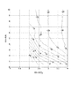
図3は、本実施形態に係る弾性表面波デバイスにおける窒化アルミニウム膜30の規格化膜厚(以降、KH‐AlNと表す:縦軸)と、二酸化シリコン膜40の規格化膜厚(以降、KH−SiO2と表す:横軸)と、音速の関係を表すグラフである。同図は窒化アルミニウム膜30の厚さをta、二酸化シリコン膜40の厚さをts、弾性表面波の波長をλとしたとき、窒化アルミニウム膜30の規格化膜厚をKH‐ALN=(2π/λ)/taとし、二酸化シリコン膜40の規格化膜厚をKH‐SiO2=(2π/λ)/taとして、縦軸をKH‐ALN、横軸をKH‐SiO2としたときのグラフを示している。図3に示すように、KH−SiO2が2.00〜4.00の測定範囲で、音速は、ほぼ5400m/s以上と十分に高い音速が得られている。
FIG. 3 shows a normalized film thickness of the aluminum nitride film 30 (hereinafter referred to as KH-AlN: vertical axis) and a normalized film thickness of the silicon dioxide film 40 (hereinafter referred to as KH) in the surface acoustic wave device according to the present embodiment. This is a graph showing the relationship between —SiO 2 : horizontal axis) and sound velocity. In the figure, when the thickness of the
図4は、本実施形態に係る弾性表面波デバイスにおけるKH‐AlNと、KH−SiO2と、遅延時間温度係数(TCD)と、の関係を示すグラフである。図4に示すように、調査した範囲(KH−SiO2が2.00〜4.00の範囲)において+20ppm/℃〜−30ppm/℃の良好な遅延時間温度係数(TCD)が得られた。 FIG. 4 is a graph showing the relationship among KH—AlN, KH—SiO 2 , and delay time temperature coefficient (TCD) in the surface acoustic wave device according to this embodiment. As shown in FIG. 4, a good delay time temperature coefficient (TCD) of +20 ppm / ° C. to −30 ppm / ° C. was obtained in the investigated range (KH—SiO 2 range of 2.00 to 4.00).
本実施形態によれば、基板としてC面サファイア基板を用いている。サファイア基板は、水晶の音速が3100m/s程度が限界とされることに対して4500m/s以上の音速が可能であることから、基板として水晶を用いる場合よりも高い音速を得られる。つまり、高周波デバイスを実現できる。 According to this embodiment, a C-plane sapphire substrate is used as the substrate. The sapphire substrate can achieve a sound speed of 4500 m / s or higher as compared to the case where the sound speed of crystal is about 3100 m / s, so that a higher sound speed can be obtained than when a crystal is used as the substrate. That is, a high frequency device can be realized.
また、窒化アルミニウムは、サファイア基板よりも電気機械結合係数(K2)が大きいこと、窒化アルミニウムをサファイア基板上に形成する場合、窒化アルミニウムの結晶性がよいことからさらに電気機械結合係数を大きくすることが可能で、弾性表面波の励振効率を高めることができる。 In addition, aluminum nitride has an electromechanical coupling coefficient (K 2 ) larger than that of the sapphire substrate, and when aluminum nitride is formed on the sapphire substrate, the crystallinity of aluminum nitride is good, so that the electromechanical coupling coefficient is further increased. It is possible to increase the surface acoustic wave excitation efficiency.
また、窒化アルミニウムは音速が5600m/sであり、C面サファイア基板の音速と窒化アルミニウムの音速とが近いため、音速差に起因する周波数変動を抑制することができる。また、従来技術のように圧電体膜として酸化亜鉛(ZnO)膜を用いると、酸化亜鉛膜は音速が3100m/sであってC面サファイア基板との音速差が大きく、高周波化を図ると音速差に起因する周波数変動が大きくなってしまう欠点がある。 Moreover, since the sound speed of aluminum nitride is 5600 m / s and the sound speed of the C-plane sapphire substrate is close to the sound speed of aluminum nitride, frequency fluctuations due to the difference in sound speed can be suppressed. Further, when a zinc oxide (ZnO) film is used as the piezoelectric film as in the prior art, the sound speed of the zinc oxide film is 3100 m / s, and the sound speed difference with the C-plane sapphire substrate is large. There is a drawback that the frequency fluctuation due to the difference becomes large.
二酸化シリコンと、窒化アルミニウムとは、逆符号の遅延時間温度係数(TCD)を有するため、良好な周波数温度特性を有することが可能となる。 Since silicon dioxide and aluminum nitride have a delay time temperature coefficient (TCD) with opposite signs, it is possible to have good frequency temperature characteristics.
また、セザワ波の1次モードを用いる場合、窒化アルミニウムの膜厚を薄くできるため、膜厚分布のばらつきを抑えることが可能で、そのことから音速(周波数)のばらつきを抑制しやすいという効果がある。 Further, when the first-order mode of Sezawa wave is used, the film thickness of aluminum nitride can be reduced, so that it is possible to suppress variations in the film thickness distribution, and thus the effect of easily suppressing variations in sound speed (frequency). is there.
なお、弾性表面波デバイス1は、固有の透過帯域を有し、しかも小型化が可能であり部品数も少ないため、通信機器用のバンドパスフィルターや基準クロックとして共振子等に応用される。フィルターや共振子に弾性表面波デバイスを用いる場合には、温度依存性を表す周波数温度係数(TCF)または遅延時間温度係数(TCD)や、電気機械変換の性能を表す電気機械結合係数(K2)が良好であることが求められる。
(実施例1)
The surface
(Example 1)
そこで、本実施形態の具体的な実施例について説明する。
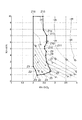
図5は、実施例1に係るKH‐AlNとKH‐SiO2と、電気機械結合係数K2との関係を示すグラフである。ここで、窒化アルミニウム膜30の厚さta、二酸化シリコン膜40の厚さts、弾性表面波の波長λ、としたとき、窒化アルミニウム膜30の規格化膜厚は、KH‐AlN=(2π/λ)・ta、二酸化シリコン膜40の規格化膜厚は、KH‐SiO2=(2π/λ)・ts、で与えられる。これら各規格化膜厚の関係を座標表示したとき、適切な領域を以下の座標で表すことができる。なお、図5では、座標1、座標2、座標3・・・をZ1、Z2、Z3・・・と表している。
Therefore, a specific example of this embodiment will be described.
FIG. 5 is a graph showing the relationship between KH—AlN and KH—SiO 2 and the electromechanical coupling coefficient K 2 according to Example 1. Here, assuming that the thickness ta of the
座標1(KH‐SiO2、KH‐AlN)=(2.00、0.88)
座標2(KH‐SiO2、KH‐AlN)=(2.50、1.13)
座標3(KH‐SiO2、KH‐AlN)=(2.76、1.42)
座標4(KH‐SiO2、KH‐AlN)=(2.77、1.75)
座標5(KH‐SiO2、KH‐AlN)=(2.60、3.00)
座標6(KH‐SiO2、KH‐AlN)=(2.57、4.00)
座標7(KH‐SiO2、KH‐AlN)=(2.60、5.00)
座標8(KH‐SiO2、KH‐AlN)=(2.74、5.96)
座標9(KH‐SiO2、KH‐AlN)=(2.80、6.83)
座標10(KH‐SiO2、KH‐AlN)=(2.80、7.83)
座標11(KH‐SiO2、KH‐AlN)=(2.82、8.67)
座標12(KH‐SiO2、KH‐AlN)=(2.82、10.00)
座標13(KH‐SiO2、KH‐AlN)=(2.00、10.00)
これらの座標を、座標1〜座標13〜座標1の順に結線した領域内で発生するセザワ波の1次モードを用いる。なお、以降、温度特性として遅延時間温度係数(TCD)を測定結果として表している。
Coordinates 1 (KH-SiO 2, KH -AlN) = (2.00,0.88)
Coordinate 2 (KH-SiO 2, KH -AlN) = (2.50,1.13)
Coordinates 3 (KH-SiO 2, KH -AlN) = (2.76,1.42)
Coordinates 4 (KH-SiO 2, KH -AlN) = (2.77,1.75)
Coordinate 5 (KH-SiO 2, KH -AlN) = (2.60,3.00)
Coordinates 6 (KH-SiO 2, KH -AlN) = (2.57,4.00)
Coordinate 7 (KH-SiO 2, KH -AlN) = (2.60,5.00)
Coordinate 8 (KH-SiO 2, KH -AlN) = (2.74,5.96)
Coordinate 9 (KH—SiO 2 , KH—AlN) = (2.80, 6.83)
Coordinates 10 (KH-SiO 2, KH -AlN) = (2.80,7.83)
Coordinates 11 (KH-SiO 2, KH -AlN) = (2.82,8.67)
Coordinate 12 (KH-SiO 2 , KH-AlN) = (2.82, 10.00)
Coordinates 13 (KH-SiO 2, KH -AlN) = (2.00,10.00)
A primary mode of Sezawa waves generated in an area where these coordinates are connected in the order of
この領域内では、電気機械結合係数K2が0.1%以上であり、弾性表面波の励振に必要とされる電気機械結合係数K2を得ることができる。
また、図3と図4の各座標系で結ばれる領域とを合成して判断すると、この領域内では、音速5600m/s以上が得られる。
(実施例2)
In this region, it is the electromechanical coupling coefficient K 2 of 0.1% or more, it is possible to obtain an electromechanical coupling coefficient K 2 required for excitation of the surface acoustic wave.
Further, if the area connected by the coordinate systems of FIGS. 3 and 4 is combined and determined, a sound speed of 5600 m / s or more is obtained in this area.
(Example 2)
次に、実施例2について説明する。実施例2は、前述した実施例1に対して遅延時間温度係数(TCD)をより向上させる範囲を発現したものである。
図6は、実施例2に係るKH‐AlNとKH‐SiO2と、遅延時間温度係数(TCD)との関係を示すグラフ、図7は電気機械結合係数K2との関係を示すグラフである。ここで、窒化アルミニウム膜30の厚さta、二酸化シリコン膜40の厚さts、弾性表面波の波長λ、としたとき、窒化アルミニウム膜30の規格化膜厚は、KH‐AlN=(2π/λ)・ta、二酸化シリコン膜40規格化膜厚は、KH‐SiO2=(2π/λ)・ts、で与えられる。これら各規格化膜厚の関係を座標表示したとき、適切な領域を以下の座標で表すことができる。なお、図6、図7では、座標1、座標2、座標3・・・をZ1、Z2、Z3・・・と表している。
Next, Example 2 will be described. Example 2 expresses a range in which the delay time temperature coefficient (TCD) is further improved as compared with Example 1 described above.
FIG. 6 is a graph showing the relationship between KH—AlN and KH—SiO 2 according to Example 2 and the delay time temperature coefficient (TCD), and FIG. 7 is a graph showing the relationship between the electromechanical coupling coefficient K 2. . Here, assuming that the thickness ta of the
座標1(KH‐SiO2、KH‐AlN)=(2.00、2.25)
座標2(KH‐SiO2、KH‐AlN)=(2.10、1.75)
座標3(KH‐SiO2、KH‐AlN)=(2.17、0.96)
座標4(KH‐SiO2、KH‐AlN)=(2.50、1.13)
座標5(KH‐SiO2、KH‐AlN)=(2.76、1.42)
座標6(KH‐SiO2、KH‐AlN)=(2.77、1.75)
座標7(KH‐SiO2、KH‐AlN)=(2.60、3.00)
座標8(KH‐SiO2、KH‐AlN)=(2.57、4.00)
座標9(KH‐SiO2、KH‐AlN)=(2.60、4.67)
座標10(KH‐SiO2、KH‐AlN)=(2.51、5.00)
座標11(KH‐SiO2、KH‐AlN)=(2.51、5.33)
座標12(KH‐SiO2、KH‐AlN)=(2.61、5.92)
座標13(KH‐SiO2、KH‐AlN)=(2.61、7.00)
座標14(KH‐SiO2、KH‐AlN)=(2.46、7.83)
座標15(KH‐SiO2、KH‐AlN)=(2.45、10.00)
座標16(KH‐SiO2、KH‐AlN)=(2.00、10.00)
これらの座標を、座標1〜座標16〜座標1の順に結線した領域内で発生するセザワ波の1次モードを用いる。
Coordinates 1 (KH-SiO 2, KH -AlN) = (2.00,2.25)
Coordinate 2 (KH-SiO 2, KH -AlN) = (2.10,1.75)
Coordinates 3 (KH-SiO 2, KH -AlN) = (2.17,0.96)
Coordinates 4 (KH-SiO 2, KH -AlN) = (2.50,1.13)
Coordinate 5 (KH-SiO 2, KH -AlN) = (2.76,1.42)
Coordinate 6 (KH—SiO 2 , KH—AlN) = (2.77, 1.75)
Coordinate 7 (KH-SiO 2, KH -AlN) = (2.60,3.00)
Coordinate 8 (KH-SiO 2, KH -AlN) = (2.57,4.00)
Coordinates 9 (KH-SiO 2, KH -AlN) = (2.60,4.67)
Coordinates 10 (KH-SiO 2, KH -AlN) = (2.51,5.00)
Coordinates 11 (KH-SiO 2, KH -AlN) = (2.51,5.33)
Coordinates 12 (KH-SiO 2, KH -AlN) = (2.61,5.92)
Coordinates 13 (KH-SiO 2, KH -AlN) = (2.61,7.00)
Coordinates 14 (KH-SiO 2, KH -AlN) = (2.46,7.83)
Coordinate 15 (KH—SiO 2 , KH—AlN) = (2.45, 10.00)
Coordinates 16 (KH-SiO 2, KH -AlN) = (2.00,10.00)
A primary mode of Sezawa waves generated in an area where these coordinates are connected in the order of
この領域内では、図6、図7に示すように、遅延時間温度係数(TCD)が、−20ppm/℃〜+20ppm/℃を得ることができる。つまり、温度依存性を表す良好な周波数温度計数(TCF)を得ることができ、電気機械結合係数K2が0.1%以上の両方を満たすことができる。
また、図3と図6の各座標系で結ばれる領域とを合成して判断すると、この領域内では、5650m/s以上の高い音速が実現でき、高周波帯域発振器に好適である。
(実施例3)
In this region, as shown in FIGS. 6 and 7, the delay time temperature coefficient (TCD) can be −20 ppm / ° C. to +20 ppm / ° C. That is, a good frequency temperature count (TCF) representing temperature dependence can be obtained, and the electromechanical coupling coefficient K 2 can satisfy both of 0.1% or more.
Further, if the area connected by the coordinate systems in FIG. 3 and FIG. 6 is combined and determined, a high sound speed of 5650 m / s or more can be realized in this area, which is suitable for a high frequency band oscillator.
(Example 3)
次に、実施例3について説明する。実施例3は、前述した実施例2に対して遅延時間温度係数(TCD)をより向上させる範囲を発現したものである。
図8は、実施例3に係るKH‐AlNとKH‐SiO2と、遅延時間温度係数(TCD)との関係を示すグラフ、図9は電気機械結合係数K2との関係を示すグラフである。ここで、窒化アルミニウム膜30の厚さta、二酸化シリコン膜40の厚さts、弾性表面波の波長λ、としたとき、窒化アルミニウム膜30の規格化膜厚は、KH‐AlN=(2π/λ)・ta、二酸化シリコン膜40の規格化膜厚は、KH‐SiO2=(2π/λ)・ts、で与えられる。これら各規格化膜厚の関係を座標表示したとき、適切な領域を以下の座標で表すことができる。なお、図8、図9では、座標1、座標2、座標3・・・をZ1、Z2、Z3・・・と表している。
Next, Example 3 will be described. Example 3 expresses a range in which the delay time temperature coefficient (TCD) is further improved compared to Example 2 described above.
FIG. 8 is a graph showing the relationship between KH—AlN and KH—SiO 2 according to Example 3 and the delay time temperature coefficient (TCD), and FIG. 9 is a graph showing the relationship between the electromechanical coupling coefficient K 2. . Here, assuming that the thickness ta of the
座標1(KH‐SiO2、KH‐AlN)=(2.00、3.46)
座標2(KH‐SiO2、KH‐AlN)=(2.27、2.00)
座標3(KH‐SiO2、KH‐AlN)=(2.50、1.13)
座標4(KH‐SiO2、KH‐AlN)=(2.76、1.42)
座標5(KH‐SiO2、KH‐AlN)=(2.77、1.75)
座標6(KH‐SiO2、KH‐AlN)=(2.62、2.83)
座標7(KH‐SiO2、KH‐AlN)=(2.41、3.50)
座標8(KH‐SiO2、KH‐AlN)=(2.00、5.92)
これらの座標を、座標1〜座標8〜座標1の順に結線した領域内で発生するセザワ波の1次モードを用いる。
Coordinates 1 (KH-SiO 2, KH -AlN) = (2.00,3.46)
Coordinate 2 (KH-SiO 2, KH -AlN) = (2.27,2.00)
Coordinates 3 (KH-SiO 2, KH -AlN) = (2.50,1.13)
Coordinate 4 (KH—SiO 2 , KH—AlN) = (2.76, 1.42)
Coordinate 5 (KH—SiO 2 , KH—AlN) = (2.77, 1.75)
Coordinate 6 (KH-SiO 2 , KH-AlN) = (2.62, 2.83)
Coordinate 7 (KH—SiO 2 , KH—AlN) = (2.41, 3.50)
Coordinate 8 (KH-SiO 2, KH -AlN) = (2.00,5.92)
A primary mode of Sezawa waves generated in an area where these coordinates are connected in the order of
この領域内では、図8、図9に示すように、遅延時間温度係数(TCD)が、−10ppm/℃〜+10ppm/℃、電気機械結合係数K2が0.1%以上の両方を満たすことができる。
また、図3と図8の各座標系で結ばれる領域とを合成して判断すると、この領域内では、5650m/s以上の高い音速が実現でき、高周波帯域発振器に好適である。
(実施例4)
In this region, as shown in FIGS. 8 and 9, the delay time temperature coefficient (TCD) satisfies both −10 ppm / ° C. to +10 ppm / ° C. and the electromechanical coupling coefficient K 2 satisfies 0.1% or more. Can do.
Further, if the area connected by the coordinate systems of FIG. 3 and FIG. 8 is synthesized and determined, a high sound speed of 5650 m / s or more can be realized in this area, which is suitable for a high frequency band oscillator.
Example 4
次に、実施例4について説明する。弾性表面波デバイスを発振器用の共振子として用いる場合には、電気機械結合係数K2を0.1%以上確保しつつ、さらに遅延時間温度係数(TCD)を小さい範囲にすることが求められる。そこで、実施例4は、前述した実施例2及び実施例3に対して電気機械結合係数K2を0.1%以上に維持すると共に、遅延時間温度係数(TCD)より小さい範囲に発現するものである。 Next, Example 4 will be described. When a surface acoustic wave device is used as a resonator for an oscillator, it is required that the delay time temperature coefficient (TCD) be set to a smaller range while ensuring an electromechanical coupling coefficient K 2 of 0.1% or more. Therefore, in the fourth embodiment, the electromechanical coupling coefficient K 2 is maintained at 0.1% or more with respect to the second and third embodiments described above, and is expressed in a range smaller than the delay time temperature coefficient (TCD). It is.
図10は、実施例4に係るKH‐AlNとKH‐SiO2と、遅延時間温度係数(TCD)との関係を示すグラフ、図11は電気機械結合係数K2との関係を示すグラフである。ここで、窒化アルミニウム膜30の厚さta、二酸化シリコン膜40の厚さts、弾性表面波の波長λ、としたとき、窒化アルミニウム膜30の規格化膜厚は、KH‐AlN=(2π/λ)・ta、二酸化シリコン膜40の規格化膜厚は、KH‐SiO2=(2π/λ)・ts、で与えられる。これら各規格化膜厚の関係を座標表示したとき、適切な領域を以下の座標で表すことができる。なお、図10、図11では、座標1、座標2、座標3・・・をZ1、Z2、Z3・・・と表している。
FIG. 10 is a graph showing the relationship between KH—AlN and KH—SiO 2 and the delay time temperature coefficient (TCD) according to Example 4, and FIG. 11 is a graph showing the relationship between the electromechanical coupling coefficient K 2. . Here, assuming that the thickness ta of the
座標1(KH‐SiO2、KH‐AlN)=(2.00、3.96)
座標2(KH‐SiO2、KH‐AlN)=(2.39、2.00)
座標3(KH‐SiO2、KH‐AlN)=(2.64、1.33)
座標4(KH‐SiO2、KH‐AlN)=(2.76、1.42)
座標5(KH‐SiO2、KH‐AlN)=(2.77、1.75)
座標6(KH‐SiO2、KH‐AlN)=(2.72、2.13)
座標7(KH‐SiO2、KH‐AlN)=(2.50、2.58)
座標8(KH‐SiO2、KH‐AlN)=(2.28、3.58)
座標9(KH‐SiO2、KH‐AlN)=(2.00、5.13)
これらの座標を、座標1〜座標9〜座標1の順に結線した領域内で発生するセザワ波の1次モードを用いる。
Coordinates 1 (KH-SiO 2, KH -AlN) = (2.00,3.96)
Coordinate 2 (KH-SiO 2, KH -AlN) = (2.39,2.00)
Coordinates 3 (KH-SiO 2, KH -AlN) = (2.64,1.33)
Coordinate 4 (KH—SiO 2 , KH—AlN) = (2.76, 1.42)
Coordinate 5 (KH—SiO 2 , KH—AlN) = (2.77, 1.75)
Coordinates 6 (KH-SiO 2, KH -AlN) = (2.72,2.13)
Coordinate 7 (KH-SiO 2, KH -AlN) = (2.50,2.58)
Coordinate 8 (KH-SiO 2, KH -AlN) = (2.28,3.58)
Coordinates 9 (KH-SiO 2, KH -AlN) = (2.00,5.13)
A primary mode of Sezawa waves generated in an area where these coordinates are connected in the order of
この領域内では、図10、図11に示すように、遅延時間温度係数(TCD)が、−5ppm/℃〜+5ppm/℃、電気機械結合係数K2が0.1%以上の両方を満たすことができる。
また、図3と図10の各座標系で結ばれる領域とを合成して判断すると、この領域内では、5650m/s以上の高い音速が実現でき、高周波帯域発振器用の発振器に好適である。
In this region, as shown in FIGS. 10 and 11, the delay time temperature coefficient (TCD) satisfies both −5 ppm / ° C. to +5 ppm / ° C. and the electromechanical coupling coefficient K 2 satisfies 0.1% or more. Can do.
Further, if the area connected by the coordinate systems of FIG. 3 and FIG. 10 is combined and determined, a high sound speed of 5650 m / s or more can be realized in this area, which is suitable for an oscillator for a high frequency band oscillator.
よって、前述した実施例1〜実施例4によれば、弾性表面波の励振に必要とされる0.1%以上の電気機械結合係数K2を確保しつつ、音速5600m/s以上で良好な温度特性を有する弾性表面波デバイスを実現できる。 Therefore, according to Examples 1 to 4 described above, the sound speed of 5600 m / s or more is good while ensuring the electromechanical coupling coefficient K 2 of 0.1% or more required for the excitation of the surface acoustic wave. A surface acoustic wave device having temperature characteristics can be realized.
なお、上述した弾性表面波デバイス1をパッケージにて密閉することで、湿気や塵埃等の外部環境からの保護を行うことで、より信頼性を高めることができる。また、以上では図1に示すような1ポートの共振子についてのみ言及してきたが、フィルターや集積回路素子と組み合わせて形成した発振器、およびモジュール装置についても本発明を適用できる。
In addition, by sealing the surface
1…弾性表面波デバイス、10…サファイア基板、11…サファイア基板の主面、21,22…櫛歯電極(IDT)、21a,22a…電極パッド、30…窒化アルミニウム膜、40…二酸化シリコン膜。
DESCRIPTION OF
Claims (8)
前記サファイア基板の主面に形成される窒化アルミニウム膜と、
前記窒化アルミニウム膜の表面に形成され弾性表面波を励振させる櫛歯電極と、
前記櫛歯電極及び前記窒化アルミニウム膜の表面を覆う二酸化シリコン膜と、
を有することを特徴とする弾性表面波デバイス。 A sapphire substrate having a C-plane as a main surface;
An aluminum nitride film formed on the main surface of the sapphire substrate;
A comb-like electrode formed on the surface of the aluminum nitride film to excite a surface acoustic wave;
A silicon dioxide film covering the surfaces of the comb electrodes and the aluminum nitride film;
A surface acoustic wave device comprising:
前記窒化アルミニウム膜の規格化膜厚をKH‐AlN=(2π/λ)・ta、
前記二酸化シリコン膜の規格化膜厚をKH‐SiO2=(2π/λ)・ts、
で与えられる各々の前記規格化膜厚の関係を座標表示したとき、
座標1(KH‐SiO2、KH‐AlN)=(2.00、0.88)
座標2(KH‐SiO2、KH‐AlN)=(2.50、1.13)
座標3(KH‐SiO2、KH‐AlN)=(2.76、1.42)
座標4(KH‐SiO2、KH‐AlN)=(2.77、1.75)
座標5(KH‐SiO2、KH‐AlN)=(2.60、3.00)
座標6(KH‐SiO2、KH‐AlN)=(2.57、4.00)
座標7(KH‐SiO2、KH‐AlN)=(2.60、5.00)
座標8(KH‐SiO2、KH‐AlN)=(2.74、5.96)
座標9(KH‐SiO2、KH‐AlN)=(2.80、6.83)
座標10(KH‐SiO2、KH‐AlN)=(2.80、7.83)
座標11(KH‐SiO2、KH‐AlN)=(2.82、8.67)
座標12(KH‐SiO2、KH‐AlN)=(2.82、10.00)
座標13(KH‐SiO2、KH‐AlN)=(2.00、10.00)
これらの座標を、座標1〜座標13の順に結ぶと共に座標13と座標1とを結んだ領域内に含まれる前記KH‐AlN及び前記KH‐SiO2を用いることを特徴とする請求項1または請求項2に記載の弾性表面波デバイス。 The thickness ta of the aluminum nitride film, the thickness ts of the silicon dioxide film, and the wavelength λ of the surface acoustic wave,
The normalized film thickness of the aluminum nitride film is KH-AlN = (2π / λ) · ta,
The normalized thickness of the silicon dioxide film is KH-SiO 2 = (2π / λ) · ts,
When the coordinates of each normalized film thickness relationship given by
Coordinates 1 (KH-SiO 2, KH -AlN) = (2.00,0.88)
Coordinate 2 (KH-SiO 2, KH -AlN) = (2.50,1.13)
Coordinates 3 (KH-SiO 2, KH -AlN) = (2.76,1.42)
Coordinates 4 (KH-SiO 2, KH -AlN) = (2.77,1.75)
Coordinate 5 (KH-SiO 2, KH -AlN) = (2.60,3.00)
Coordinates 6 (KH-SiO 2, KH -AlN) = (2.57,4.00)
Coordinate 7 (KH-SiO 2, KH -AlN) = (2.60,5.00)
Coordinate 8 (KH-SiO 2, KH -AlN) = (2.74,5.96)
Coordinate 9 (KH—SiO 2 , KH—AlN) = (2.80, 6.83)
Coordinates 10 (KH-SiO 2, KH -AlN) = (2.80,7.83)
Coordinates 11 (KH-SiO 2, KH -AlN) = (2.82,8.67)
Coordinate 12 (KH-SiO 2 , KH-AlN) = (2.82, 10.00)
Coordinates 13 (KH-SiO 2, KH -AlN) = (2.00,10.00)
The KH-AlN and the KH-SiO 2 included in a region connecting the coordinates 13 and the coordinates 1 and connecting these coordinates in the order of coordinates 1 to 13 are used. Item 3. The surface acoustic wave device according to Item 2.
前記窒化アルミニウム膜の規格化膜厚をKH‐AlN=(2π/λ)・ta、
前記二酸化シリコン膜の規格化膜厚をKH‐SiO2=(2π/λ)・ts、
で与えられる各々の前記規格化膜厚の関係を座標表示したとき、
座標1(KH‐SiO2、KH‐AlN)=(2.00、2.25)
座標2(KH‐SiO2、KH‐AlN)=(2.10、1.75)
座標3(KH‐SiO2、KH‐AlN)=(2.17、0.96)
座標4(KH‐SiO2、KH‐AlN)=(2.50、1.13)
座標5(KH‐SiO2、KH‐AlN)=(2.76、1.42)
座標6(KH‐SiO2、KH‐AlN)=(2.77、1.75)
座標7(KH‐SiO2、KH‐AlN)=(2.60、3.00)
座標8(KH‐SiO2、KH‐AlN)=(2.57、4.00)
座標9(KH‐SiO2、KH‐AlN)=(2.60、4.67)
座標10(KH‐SiO2、KH‐AlN)=(2.51、5.00)
座標11(KH‐SiO2、KH‐AlN)=(2.51、5.33)
座標12(KH‐SiO2、KH‐AlN)=(2.61、5.92)
座標13(KH‐SiO2、KH‐AlN)=(2.61、7.00)
座標14(KH‐SiO2、KH‐AlN)=(2.46、7.83)
座標15(KH‐SiO2、KH‐AlN)=(2.45、10.00)
座標16(KH‐SiO2、KH‐AlN)=(2.00、10.00)
これらの座標を、座標1〜座標16の順に結ぶと共に座標16と座標1とを結んだ領域内に含まれる前記KH‐AlN及び前記KH‐SiO2を用いることを特徴とする請求項1または請求項2に記載の弾性表面波デバイス。 The thickness ta of the aluminum nitride film, the thickness ts of the silicon dioxide film, and the wavelength λ of the surface acoustic wave,
The normalized film thickness of the aluminum nitride film is KH-AlN = (2π / λ) · ta,
The normalized thickness of the silicon dioxide film is KH-SiO 2 = (2π / λ) · ts,
When the coordinates of each normalized film thickness relationship given by
Coordinates 1 (KH-SiO 2, KH -AlN) = (2.00,2.25)
Coordinate 2 (KH-SiO 2, KH -AlN) = (2.10,1.75)
Coordinates 3 (KH-SiO 2, KH -AlN) = (2.17,0.96)
Coordinates 4 (KH-SiO 2, KH -AlN) = (2.50,1.13)
Coordinate 5 (KH-SiO 2, KH -AlN) = (2.76,1.42)
Coordinate 6 (KH—SiO 2 , KH—AlN) = (2.77, 1.75)
Coordinate 7 (KH-SiO 2, KH -AlN) = (2.60,3.00)
Coordinate 8 (KH-SiO 2, KH -AlN) = (2.57,4.00)
Coordinates 9 (KH-SiO 2, KH -AlN) = (2.60,4.67)
Coordinates 10 (KH-SiO 2, KH -AlN) = (2.51,5.00)
Coordinates 11 (KH-SiO 2, KH -AlN) = (2.51,5.33)
Coordinates 12 (KH-SiO 2, KH -AlN) = (2.61,5.92)
Coordinates 13 (KH-SiO 2, KH -AlN) = (2.61,7.00)
Coordinates 14 (KH-SiO 2, KH -AlN) = (2.46,7.83)
Coordinate 15 (KH—SiO 2 , KH—AlN) = (2.45, 10.00)
Coordinates 16 (KH-SiO 2, KH -AlN) = (2.00,10.00)
The KH-AlN and the KH-SiO 2 included in a region where the coordinates are connected in the order of coordinates 1 to 16 and the coordinates 16 and 1 are connected are used. Item 3. The surface acoustic wave device according to Item 2.
前記窒化アルミニウム膜の規格化膜厚をKH‐AlN=(2π/λ)・ta、
前記二酸化シリコン膜の規格化膜厚をKH‐SiO2=(2π/λ)・ts、
で与えられる各々の前記規格化膜厚の関係を座標表示したとき、
座標1(KH‐SiO2、KH‐AlN)=(2.00、3.46)
座標2(KH‐SiO2、KH‐AlN)=(2.27、2.00)
座標3(KH‐SiO2、KH‐AlN)=(2.50、1.13)
座標4(KH‐SiO2、KH‐AlN)=(2.76、1.42)
座標5(KH‐SiO2、KH‐AlN)=(2.77、1.75)
座標6(KH‐SiO2、KH‐AlN)=(2.62、2.83)
座標7(KH‐SiO2、KH‐AlN)=(2.41、3.50)
座標8(KH‐SiO2、KH‐AlN)=(2.00、5.92)
これらの座標を、座標1〜座標8の順に結ぶと共に座標8と座標1とを結んだ領域内に含まれる前記KH‐AlN及び前記KH‐SiO2を用いることを特徴とする請求項1または請求項2に記載の弾性表面波デバイス。 The thickness ta of the aluminum nitride film, the thickness ts of the silicon dioxide film, and the wavelength λ of the surface acoustic wave,
The normalized film thickness of the aluminum nitride film is KH-AlN = (2π / λ) · ta,
The normalized thickness of the silicon dioxide film is KH-SiO 2 = (2π / λ) · ts,
When the coordinates of each normalized film thickness relationship given by
Coordinates 1 (KH-SiO 2, KH -AlN) = (2.00,3.46)
Coordinate 2 (KH-SiO 2, KH -AlN) = (2.27,2.00)
Coordinates 3 (KH-SiO 2, KH -AlN) = (2.50,1.13)
Coordinate 4 (KH—SiO 2 , KH—AlN) = (2.76, 1.42)
Coordinate 5 (KH—SiO 2 , KH—AlN) = (2.77, 1.75)
Coordinate 6 (KH-SiO 2 , KH-AlN) = (2.62, 2.83)
Coordinate 7 (KH—SiO 2 , KH—AlN) = (2.41, 3.50)
Coordinate 8 (KH-SiO 2, KH -AlN) = (2.00,5.92)
The KH-AlN and the KH-SiO 2 included in a region where the coordinates are connected in the order of coordinates 1 to 8 and the coordinates 8 and 1 are connected are used. Item 3. The surface acoustic wave device according to Item 2.
前記窒化アルミニウム膜の規格化膜厚をKH‐AlN=(2π/λ)・ta、
前記二酸化シリコン膜の規格化膜厚をKH‐SiO2=(2π/λ)・ts、
で与えられる各々の前記規格化膜厚の関係を座標表示したとき、
座標1(KH‐SiO2、KH‐AlN)=(2.00、3.96)
座標2(KH‐SiO2、KH‐AlN)=(2.39、2.00)
座標3(KH‐SiO2、KH‐AlN)=(2.64、1.33)
座標4(KH‐SiO2、KH‐AlN)=(2.76、1.42)
座標5(KH‐SiO2、KH‐AlN)=(2.77、1.75)
座標6(KH‐SiO2、KH‐AlN)=(2.72、2.13)
座標7(KH‐SiO2、KH‐AlN)=(2.50、2.58)
座標8(KH‐SiO2、KH‐AlN)=(2.28、3.58)
座標9(KH‐SiO2、KH‐AlN)=(2.00、5.13)
これらの座標を、座標1〜座標9の順に結ぶと共に座標9と座標1とを結んだ領域内に含まれる前記KH‐AlN及び前記KH‐SiO2でを用いることを特徴とする請求項1または請求項2に記載の弾性表面波デバイス。 The thickness ta of the aluminum nitride film, the thickness ts of the silicon dioxide film, and the wavelength λ of the surface acoustic wave,
The normalized film thickness of the aluminum nitride film is KH-AlN = (2π / λ) · ta,
The normalized thickness of the silicon dioxide film is KH-SiO 2 = (2π / λ) · ts,
When the coordinates of each normalized film thickness relationship given by
Coordinates 1 (KH-SiO 2, KH -AlN) = (2.00,3.96)
Coordinate 2 (KH-SiO 2, KH -AlN) = (2.39,2.00)
Coordinates 3 (KH-SiO 2, KH -AlN) = (2.64,1.33)
Coordinate 4 (KH—SiO 2 , KH—AlN) = (2.76, 1.42)
Coordinate 5 (KH—SiO 2 , KH—AlN) = (2.77, 1.75)
Coordinates 6 (KH-SiO 2, KH -AlN) = (2.72,2.13)
Coordinate 7 (KH-SiO 2, KH -AlN) = (2.50,2.58)
Coordinate 8 (KH-SiO 2, KH -AlN) = (2.28,3.58)
Coordinates 9 (KH-SiO 2, KH -AlN) = (2.00,5.13)
2. These coordinates are connected in the order of coordinates 1 to 9 and are used in the KH-AlN and the KH-SiO 2 included in the region connecting the coordinates 9 and the coordinates 1. The surface acoustic wave device according to claim 2.
Priority Applications (2)
| Application Number | Priority Date | Filing Date | Title |
|---|---|---|---|
| JP2009297056A JP2011139215A (en) | 2009-12-28 | 2009-12-28 | Surface acoustic wave device, oscillator, and module apparatus |
| US12/977,525 US8624690B2 (en) | 2009-12-28 | 2010-12-23 | Surface acoustic wave device, oscillator, module apparatus |
Applications Claiming Priority (1)
| Application Number | Priority Date | Filing Date | Title |
|---|---|---|---|
| JP2009297056A JP2011139215A (en) | 2009-12-28 | 2009-12-28 | Surface acoustic wave device, oscillator, and module apparatus |
Publications (2)
| Publication Number | Publication Date |
|---|---|
| JP2011139215A true JP2011139215A (en) | 2011-07-14 |
| JP2011139215A5 JP2011139215A5 (en) | 2012-08-30 |
Family
ID=44350211
Family Applications (1)
| Application Number | Title | Priority Date | Filing Date |
|---|---|---|---|
| JP2009297056A Withdrawn JP2011139215A (en) | 2009-12-28 | 2009-12-28 | Surface acoustic wave device, oscillator, and module apparatus |
Country Status (1)
| Country | Link |
|---|---|
| JP (1) | JP2011139215A (en) |
Citations (4)
| Publication number | Priority date | Publication date | Assignee | Title |
|---|---|---|---|---|
| JPH04109709A (en) * | 1990-08-29 | 1992-04-10 | Sanyo Electric Co Ltd | Surface acoustic wave element |
| JPH08316779A (en) * | 1995-05-15 | 1996-11-29 | Sanyo Electric Co Ltd | Surface acoustic wave element |
| JP2002152000A (en) * | 2000-11-14 | 2002-05-24 | Seiko Epson Corp | Surface acoustic wave element |
| JP2008244523A (en) * | 2007-03-23 | 2008-10-09 | Seiko Epson Corp | Surface acoustic wave element and electronic equipment |
-
2009
- 2009-12-28 JP JP2009297056A patent/JP2011139215A/en not_active Withdrawn
Patent Citations (4)
| Publication number | Priority date | Publication date | Assignee | Title |
|---|---|---|---|---|
| JPH04109709A (en) * | 1990-08-29 | 1992-04-10 | Sanyo Electric Co Ltd | Surface acoustic wave element |
| JPH08316779A (en) * | 1995-05-15 | 1996-11-29 | Sanyo Electric Co Ltd | Surface acoustic wave element |
| JP2002152000A (en) * | 2000-11-14 | 2002-05-24 | Seiko Epson Corp | Surface acoustic wave element |
| JP2008244523A (en) * | 2007-03-23 | 2008-10-09 | Seiko Epson Corp | Surface acoustic wave element and electronic equipment |
Similar Documents
| Publication | Publication Date | Title |
|---|---|---|
| JP6856825B2 (en) | Elastic wave device, demultiplexer and communication device | |
| KR100858324B1 (en) | Surface Acoustic Wave device | |
| EP1610460B1 (en) | Elastic boundary wave device | |
| US9048813B2 (en) | Acoustic wave device and antenna duplexer using the same | |
| US7355319B2 (en) | Boundary acoustic wave device | |
| JP3278167B2 (en) | Surface acoustic wave device | |
| JP2015537492A (en) | Electronic acoustic parts | |
| US8773000B2 (en) | Acoustic wave device | |
| US9843304B2 (en) | Transducer with bulk waves surface-guided by synchronous excitation structures | |
| Vidal-Álvarez et al. | Delay lines based on a suspended thin film of X-cut lithium niobate | |
| US11437973B2 (en) | Surface acoustic wave device on composite substrate | |
| JP2007142794A (en) | Surface acoustic wave element chip and surface acoustic wave device | |
| JP2007124627A (en) | Surface acoustic wave device, module device, oscillation circuit and method for manufacturing surface acoustic wave device | |
| JP2019201345A (en) | Acoustic wave resonator, filter and multiplexer | |
| JP2014504827A (en) | Surface acoustic wave filter | |
| JP2002152000A (en) | Surface acoustic wave element | |
| KR20080008396A (en) | Boundary acoustic wave device | |
| US8624690B2 (en) | Surface acoustic wave device, oscillator, module apparatus | |
| US8674790B2 (en) | Surface acoustic wave device, oscillator, module apparatus | |
| JP2011176546A (en) | Surface acoustic wave device, oscillator, module apparatus | |
| JP2002141768A (en) | Surface acoustic wave element | |
| JP2011139215A (en) | Surface acoustic wave device, oscillator, and module apparatus | |
| JP2011139214A (en) | Surface acoustic wave device, oscillator, and module apparatus | |
| JP2011166567A (en) | Surface acoustic wave device, oscillator, and module apparatus | |
| JP2011151641A (en) | Surface acoustic wave device, oscillator, and module device |
Legal Events
| Date | Code | Title | Description |
|---|---|---|---|
| A521 | Request for written amendment filed |
Free format text: JAPANESE INTERMEDIATE CODE: A523 Effective date: 20120711 |
|
| A621 | Written request for application examination |
Free format text: JAPANESE INTERMEDIATE CODE: A621 Effective date: 20120711 |
|
| A977 | Report on retrieval |
Free format text: JAPANESE INTERMEDIATE CODE: A971007 Effective date: 20130308 |
|
| A131 | Notification of reasons for refusal |
Free format text: JAPANESE INTERMEDIATE CODE: A131 Effective date: 20130319 |
|
| A761 | Written withdrawal of application |
Free format text: JAPANESE INTERMEDIATE CODE: A761 Effective date: 20130510 |