JP2010535359A - 光管理アセンブリ - Google Patents
光管理アセンブリ Download PDFInfo
- Publication number
- JP2010535359A JP2010535359A JP2010520029A JP2010520029A JP2010535359A JP 2010535359 A JP2010535359 A JP 2010535359A JP 2010520029 A JP2010520029 A JP 2010520029A JP 2010520029 A JP2010520029 A JP 2010520029A JP 2010535359 A JP2010535359 A JP 2010535359A
- Authority
- JP
- Japan
- Prior art keywords
- light
- film
- cover film
- transmissive plate
- management assembly
- Prior art date
- Legal status (The legal status is an assumption and is not a legal conclusion. Google has not performed a legal analysis and makes no representation as to the accuracy of the status listed.)
- Pending
Links
- 239000013039 cover film Substances 0.000 claims abstract description 135
- 239000012788 optical film Substances 0.000 claims abstract description 115
- NIXOWILDQLNWCW-UHFFFAOYSA-N acrylic acid group Chemical group C(C=C)(=O)O NIXOWILDQLNWCW-UHFFFAOYSA-N 0.000 claims description 6
- 239000004793 Polystyrene Substances 0.000 claims description 3
- 229920000515 polycarbonate Polymers 0.000 claims description 3
- 239000004417 polycarbonate Substances 0.000 claims description 3
- 229920002223 polystyrene Polymers 0.000 claims description 3
- 229920000728 polyester Polymers 0.000 claims description 2
- 229920000098 polyolefin Polymers 0.000 claims description 2
- 239000004973 liquid crystal related substance Substances 0.000 abstract description 8
- 238000004519 manufacturing process Methods 0.000 abstract description 3
- 239000010408 film Substances 0.000 description 109
- 230000003287 optical effect Effects 0.000 description 23
- 239000000523 sample Substances 0.000 description 18
- 230000007613 environmental effect Effects 0.000 description 13
- 239000004820 Pressure-sensitive adhesive Substances 0.000 description 8
- 238000000034 method Methods 0.000 description 8
- 238000012360 testing method Methods 0.000 description 8
- 238000009792 diffusion process Methods 0.000 description 6
- 239000000463 material Substances 0.000 description 6
- 230000010287 polarization Effects 0.000 description 6
- -1 polyethylene terephthalate Polymers 0.000 description 6
- 239000000853 adhesive Substances 0.000 description 5
- 230000001070 adhesive effect Effects 0.000 description 5
- 239000011248 coating agent Substances 0.000 description 5
- 238000000576 coating method Methods 0.000 description 5
- 238000010521 absorption reaction Methods 0.000 description 4
- 230000000740 bleeding effect Effects 0.000 description 4
- 230000008859 change Effects 0.000 description 4
- 230000003098 cholesteric effect Effects 0.000 description 4
- 230000007547 defect Effects 0.000 description 4
- 230000008569 process Effects 0.000 description 4
- 230000000007 visual effect Effects 0.000 description 4
- 230000008901 benefit Effects 0.000 description 3
- 230000005540 biological transmission Effects 0.000 description 3
- 230000000052 comparative effect Effects 0.000 description 3
- 239000000835 fiber Substances 0.000 description 3
- 239000005020 polyethylene terephthalate Substances 0.000 description 3
- 229920000139 polyethylene terephthalate Polymers 0.000 description 3
- 230000001902 propagating effect Effects 0.000 description 3
- 230000001681 protective effect Effects 0.000 description 3
- 239000000758 substrate Substances 0.000 description 3
- VTYYLEPIZMXCLO-UHFFFAOYSA-L Calcium carbonate Chemical compound [Ca+2].[O-]C([O-])=O VTYYLEPIZMXCLO-UHFFFAOYSA-L 0.000 description 2
- 239000004743 Polypropylene Substances 0.000 description 2
- GWEVSGVZZGPLCZ-UHFFFAOYSA-N Titan oxide Chemical compound O=[Ti]=O GWEVSGVZZGPLCZ-UHFFFAOYSA-N 0.000 description 2
- TZCXTZWJZNENPQ-UHFFFAOYSA-L barium sulfate Chemical compound [Ba+2].[O-]S([O-])(=O)=O TZCXTZWJZNENPQ-UHFFFAOYSA-L 0.000 description 2
- 239000011324 bead Substances 0.000 description 2
- 239000002131 composite material Substances 0.000 description 2
- 239000007789 gas Substances 0.000 description 2
- 238000009499 grossing Methods 0.000 description 2
- 238000005286 illumination Methods 0.000 description 2
- 230000001788 irregular Effects 0.000 description 2
- 238000005259 measurement Methods 0.000 description 2
- 229920000642 polymer Polymers 0.000 description 2
- 229920001155 polypropylene Polymers 0.000 description 2
- 238000007789 sealing Methods 0.000 description 2
- 238000000926 separation method Methods 0.000 description 2
- 239000000126 substance Substances 0.000 description 2
- 230000037303 wrinkles Effects 0.000 description 2
- SMZOUWXMTYCWNB-UHFFFAOYSA-N 2-(2-methoxy-5-methylphenyl)ethanamine Chemical compound COC1=CC=C(C)C=C1CCN SMZOUWXMTYCWNB-UHFFFAOYSA-N 0.000 description 1
- DXPPIEDUBFUSEZ-UHFFFAOYSA-N 6-methylheptyl prop-2-enoate Chemical compound CC(C)CCCCCOC(=O)C=C DXPPIEDUBFUSEZ-UHFFFAOYSA-N 0.000 description 1
- 229920006257 Heat-shrinkable film Polymers 0.000 description 1
- 239000004831 Hot glue Substances 0.000 description 1
- CERQOIWHTDAKMF-UHFFFAOYSA-M Methacrylate Chemical compound CC(=C)C([O-])=O CERQOIWHTDAKMF-UHFFFAOYSA-M 0.000 description 1
- 239000004698 Polyethylene Substances 0.000 description 1
- 230000004913 activation Effects 0.000 description 1
- 230000004075 alteration Effects 0.000 description 1
- 229920006125 amorphous polymer Polymers 0.000 description 1
- 230000000844 anti-bacterial effect Effects 0.000 description 1
- 238000013459 approach Methods 0.000 description 1
- 229910000019 calcium carbonate Inorganic materials 0.000 description 1
- 238000005266 casting Methods 0.000 description 1
- 239000013068 control sample Substances 0.000 description 1
- 229920001577 copolymer Polymers 0.000 description 1
- 230000008878 coupling Effects 0.000 description 1
- 238000010168 coupling process Methods 0.000 description 1
- 238000005859 coupling reaction Methods 0.000 description 1
- 238000002788 crimping Methods 0.000 description 1
- 230000009977 dual effect Effects 0.000 description 1
- 230000000694 effects Effects 0.000 description 1
- 229920006332 epoxy adhesive Polymers 0.000 description 1
- 239000011521 glass Substances 0.000 description 1
- 238000010438 heat treatment Methods 0.000 description 1
- 238000003475 lamination Methods 0.000 description 1
- 239000002184 metal Substances 0.000 description 1
- 229910052751 metal Inorganic materials 0.000 description 1
- 239000012229 microporous material Substances 0.000 description 1
- 230000000116 mitigating effect Effects 0.000 description 1
- 239000000203 mixture Substances 0.000 description 1
- 238000012986 modification Methods 0.000 description 1
- 230000004048 modification Effects 0.000 description 1
- 238000004806 packaging method and process Methods 0.000 description 1
- 239000002245 particle Substances 0.000 description 1
- 239000004033 plastic Substances 0.000 description 1
- 229920003023 plastic Polymers 0.000 description 1
- 229920003207 poly(ethylene-2,6-naphthalate) Polymers 0.000 description 1
- 229920000573 polyethylene Polymers 0.000 description 1
- 239000011112 polyethylene naphthalate Substances 0.000 description 1
- 239000004810 polytetrafluoroethylene Substances 0.000 description 1
- 229920001343 polytetrafluoroethylene Polymers 0.000 description 1
- 238000002360 preparation method Methods 0.000 description 1
- 239000013074 reference sample Substances 0.000 description 1
- 238000011160 research Methods 0.000 description 1
- 239000005060 rubber Substances 0.000 description 1
- 229920006126 semicrystalline polymer Polymers 0.000 description 1
- 229920006300 shrink film Polymers 0.000 description 1
- 230000001629 suppression Effects 0.000 description 1
- 238000010998 test method Methods 0.000 description 1
- 229920001187 thermosetting polymer Polymers 0.000 description 1
- 239000004408 titanium dioxide Substances 0.000 description 1
Images


Classifications
-
- G—PHYSICS
- G02—OPTICS
- G02F—OPTICAL DEVICES OR ARRANGEMENTS FOR THE CONTROL OF LIGHT BY MODIFICATION OF THE OPTICAL PROPERTIES OF THE MEDIA OF THE ELEMENTS INVOLVED THEREIN; NON-LINEAR OPTICS; FREQUENCY-CHANGING OF LIGHT; OPTICAL LOGIC ELEMENTS; OPTICAL ANALOGUE/DIGITAL CONVERTERS
- G02F1/00—Devices or arrangements for the control of the intensity, colour, phase, polarisation or direction of light arriving from an independent light source, e.g. switching, gating or modulating; Non-linear optics
- G02F1/01—Devices or arrangements for the control of the intensity, colour, phase, polarisation or direction of light arriving from an independent light source, e.g. switching, gating or modulating; Non-linear optics for the control of the intensity, phase, polarisation or colour
- G02F1/13—Devices or arrangements for the control of the intensity, colour, phase, polarisation or direction of light arriving from an independent light source, e.g. switching, gating or modulating; Non-linear optics for the control of the intensity, phase, polarisation or colour based on liquid crystals, e.g. single liquid crystal display cells
- G02F1/133—Constructional arrangements; Operation of liquid crystal cells; Circuit arrangements
- G02F1/1333—Constructional arrangements; Manufacturing methods
- G02F1/1335—Structural association of cells with optical devices, e.g. polarisers or reflectors
- G02F1/1336—Illuminating devices
- G02F1/133602—Direct backlight
- G02F1/133604—Direct backlight with lamps
-
- G—PHYSICS
- G02—OPTICS
- G02B—OPTICAL ELEMENTS, SYSTEMS OR APPARATUS
- G02B6/00—Light guides; Structural details of arrangements comprising light guides and other optical elements, e.g. couplings
- G02B6/0001—Light guides; Structural details of arrangements comprising light guides and other optical elements, e.g. couplings specially adapted for lighting devices or systems
- G02B6/0011—Light guides; Structural details of arrangements comprising light guides and other optical elements, e.g. couplings specially adapted for lighting devices or systems the light guides being planar or of plate-like form
- G02B6/0033—Means for improving the coupling-out of light from the light guide
- G02B6/005—Means for improving the coupling-out of light from the light guide provided by one optical element, or plurality thereof, placed on the light output side of the light guide
- G02B6/0053—Prismatic sheet or layer; Brightness enhancement element, sheet or layer
-
- G—PHYSICS
- G02—OPTICS
- G02B—OPTICAL ELEMENTS, SYSTEMS OR APPARATUS
- G02B6/00—Light guides; Structural details of arrangements comprising light guides and other optical elements, e.g. couplings
- G02B6/0001—Light guides; Structural details of arrangements comprising light guides and other optical elements, e.g. couplings specially adapted for lighting devices or systems
- G02B6/0011—Light guides; Structural details of arrangements comprising light guides and other optical elements, e.g. couplings specially adapted for lighting devices or systems the light guides being planar or of plate-like form
- G02B6/0033—Means for improving the coupling-out of light from the light guide
- G02B6/0056—Means for improving the coupling-out of light from the light guide for producing polarisation effects, e.g. by a surface with polarizing properties or by an additional polarizing elements
-
- G—PHYSICS
- G02—OPTICS
- G02F—OPTICAL DEVICES OR ARRANGEMENTS FOR THE CONTROL OF LIGHT BY MODIFICATION OF THE OPTICAL PROPERTIES OF THE MEDIA OF THE ELEMENTS INVOLVED THEREIN; NON-LINEAR OPTICS; FREQUENCY-CHANGING OF LIGHT; OPTICAL LOGIC ELEMENTS; OPTICAL ANALOGUE/DIGITAL CONVERTERS
- G02F1/00—Devices or arrangements for the control of the intensity, colour, phase, polarisation or direction of light arriving from an independent light source, e.g. switching, gating or modulating; Non-linear optics
- G02F1/01—Devices or arrangements for the control of the intensity, colour, phase, polarisation or direction of light arriving from an independent light source, e.g. switching, gating or modulating; Non-linear optics for the control of the intensity, phase, polarisation or colour
- G02F1/13—Devices or arrangements for the control of the intensity, colour, phase, polarisation or direction of light arriving from an independent light source, e.g. switching, gating or modulating; Non-linear optics for the control of the intensity, phase, polarisation or colour based on liquid crystals, e.g. single liquid crystal display cells
- G02F1/133—Constructional arrangements; Operation of liquid crystal cells; Circuit arrangements
- G02F1/1333—Constructional arrangements; Manufacturing methods
- G02F1/1335—Structural association of cells with optical devices, e.g. polarisers or reflectors
- G02F1/133504—Diffusing, scattering, diffracting elements
- G02F1/133507—Films for enhancing the luminance
-
- G—PHYSICS
- G02—OPTICS
- G02F—OPTICAL DEVICES OR ARRANGEMENTS FOR THE CONTROL OF LIGHT BY MODIFICATION OF THE OPTICAL PROPERTIES OF THE MEDIA OF THE ELEMENTS INVOLVED THEREIN; NON-LINEAR OPTICS; FREQUENCY-CHANGING OF LIGHT; OPTICAL LOGIC ELEMENTS; OPTICAL ANALOGUE/DIGITAL CONVERTERS
- G02F1/00—Devices or arrangements for the control of the intensity, colour, phase, polarisation or direction of light arriving from an independent light source, e.g. switching, gating or modulating; Non-linear optics
- G02F1/01—Devices or arrangements for the control of the intensity, colour, phase, polarisation or direction of light arriving from an independent light source, e.g. switching, gating or modulating; Non-linear optics for the control of the intensity, phase, polarisation or colour
- G02F1/13—Devices or arrangements for the control of the intensity, colour, phase, polarisation or direction of light arriving from an independent light source, e.g. switching, gating or modulating; Non-linear optics for the control of the intensity, phase, polarisation or colour based on liquid crystals, e.g. single liquid crystal display cells
- G02F1/133—Constructional arrangements; Operation of liquid crystal cells; Circuit arrangements
- G02F1/1333—Constructional arrangements; Manufacturing methods
- G02F1/1335—Structural association of cells with optical devices, e.g. polarisers or reflectors
- G02F1/1336—Illuminating devices
- G02F1/133602—Direct backlight
- G02F1/133606—Direct backlight including a specially adapted diffusing, scattering or light controlling members
Landscapes
- Physics & Mathematics (AREA)
- Nonlinear Science (AREA)
- Mathematical Physics (AREA)
- Chemical & Material Sciences (AREA)
- Crystallography & Structural Chemistry (AREA)
- General Physics & Mathematics (AREA)
- Optics & Photonics (AREA)
- Liquid Crystal (AREA)
- Planar Illumination Modules (AREA)
- Optical Elements Other Than Lenses (AREA)
- Polarising Elements (AREA)
Abstract
Description
外観試験
外観試験(VA)は、光管理アセンブリが一様な外観、つまり視覚的欠陥を持たない外観を呈するか否かについての判定である。一様な外観の欠如は、ディスプレイの区域内における視覚的相違という形をなし得る。視覚的欠陥の一例が、顕著なにじみ領域である。にじみ領域は、その周りの区域とは異なって見え、おそらくはニュートン環現象又は輝度の変化を示す。他の視覚的欠陥には、光学フィルムの縮れ及び積層されたフィルム間の気泡によって生じるものが挙げられる。特定の条件により、フィルムが縮れて、シートの大部分から隆起した領域を示すことがある。積層されたフィルムの間の気泡は、輝度の顕著な変化を生じる。
完全を期して具体的な詳細が与えられているが、同様の結果が、他の商業的に入手可能な設備を使用する以下の手法の変形形態を利用して達成され得ることは、容易に認められよう。
400グリットのサンドペーパーを使用して縁部を平滑化することによって、光透過性プレートを用意した。光透過性プレートの角部に、400グリットのサンドペーパーを使用してわずかに丸みを付けた。導光プレートを使用する場合には、平滑化も丸み付けも実施しなかった。粘着ローラー(スコットランド、インチナン(Inchinnan)のテクネック社(Teknek)製のDCRクリーンローラーシステム)を使用して、光透過性プレートからくずを取り除いた。カバーフィルムの大き目の寸法の一片を、カバーフィルムのロールから切断した。(例えば、27.9cm×55.9cm(11インチ×22インチ)の光透過性プレートは、予め折り畳まれたカバーフィルムの約76.2cm(30インチ)長の片に対し、折り畳まれたフィルムの45.7cm(18インチ)幅のロールを必要とする)。次いで、予め折り畳まれたフィルムの一方の側を、インパルスシーラー(イタリア国のミニパック・トーレシステムズ社(Minipak-Torre Systems)から入手可能なHeat Shrink Replay 55)を使用して折り目に垂直に溶着して、L字形状のポケットを形成した。くずの無いプレートをフィルムのポケットの中に滑り込ませ、「L字」の角部にしっかりと押し込んだ。次いで、プレートを収容したフィルムのポケットを、フィルム内での遊びを最小量にしてインパルスシーラーの中に配置して、フィルムの残り2つの開いた縁部を溶着した。次いで、フィルムで覆われたプレートを約93℃の温度のオーブン内に配置して、プレートの周りにカバーフィルムを収縮させた。フィルム内の残存するしわを取り除くために、ホットエアガン(ミネソタ州プリマス(Plymouth)のMHTプロダクツ社(MHT Products Inc.)製のModel 750 Heat Gun)を使用してフィルムの「しわが寄った」領域を暖めて、しわを収縮させた。
3M(商標)ビキュイティ(Vikuiti)(商標)Dual Brightness Enhancement Film(DBEF−Q)の一方の側を、実質的に、2006年6月30日に出願された米国特許出願第11/427948号に記載されている通りに、ビーズ入りの拡散体溶液でコーティングし乾燥させた。次いで、フィルムの反対側を、アクリル系感圧性接着剤(PSA)の溶液で(以下に実施例1〜9で説明するように)コーティングし乾燥させ、次いで、保護ライナーで覆ってPSAコーティングを保護した。基材への積層の前に、保護ライナーを除去した。

艶消し仕上げした光透過性プレート(日本国東京都の住友化学社(Sumitomo Chemical Company)によるモデル番号RM802)を、上述の通りに様々な収縮包装カバーフィルムで包んだ。ビーズ入りの拡散体コーティングを一方の側に、アクリル系PSAをもう一方の側に有するDBEFフィルムを、上述の通りに調製した。アクリル系PSAは、イソオクチルアクリレートとアクリル酸とのコポリマー(90:10)であり、30部のPinecrystal(商標)KE−311(イリノイ州シカゴ(Chicago)のアラカワケミカル(USA)社(Arakawa Chemical(USA)Inc))を含有するものであった。偏光フィルムを、光透過性プレートの出力側でカバーフィルムに積層した。対照は、カバーフィルムを用いておらず、同じ艶消し仕上げされた光透過性プレートと、同じDBEFとの層状アセンブリであった。各サンプルごとの相対光学ゲインを第1表に示す。
更にBEFフィルムを光透過性プレートの出力表面とカバーフィルムとの間に加えたことを除いて、実施例10で上述した通りに光管理アセンブリを調製した。相対光学ゲインは0.98であった。対照アセンブリ(カバーフィルムがなく、DBEFフィルム上にPSAがない別々の試験片)の相対光学ゲインは1であった。
光透過性プレートが49.6cm×28.3cm×0.2cmの寸法を有していたことを除いて、実施例9で上述した通りに光管理アセンブリを調製した。光管理アセンブリを、実際のバックライトハウジングのフレームに類似したフレーム内に配置し、環境試験チャンバ(ミシガン州グランドラピッズ(Grand Rapids)のエンバイロトロニクス社(Envirotronics)のモデル番号FLX900−2−6−WC)内に配置した。アセンブリを、65℃、95%の相対湿度の環境条件に100時間、次いで90℃に24時間にわたって暴露した。双方の環境条件の間及び後に、アセンブリは優の外観を示し、軽度のプレート変形のみを伴った。
艶消し仕上げした拡散フィルム(両面に艶消し仕上げを有する、アップル(Apple)(商標)社の30.5cm(12インチ)径のMac(商標)Powerbook(商標)ラップトップコンピュータから得た拡散体)を導光プレート(前述のラップトップコンピュータから得た)の平滑な表面上に、そして2片のBEFフィルムを艶消し仕上げされた拡散フィルムの上に配置することによって、光管理アセンブリを調製した。プレート及びフィルムを、上述の通りに75 LEFカバーフィルムで包んだ。カバーフィルムは、加熱及び収縮の後にぴんと張った。BEFフィルム上の尖った構造は、第1のBEFフィルムと第2のBEFフィルムとの間、及び上部のBEFフィルムと収縮包装の包みとの間の間隙を実質的に維持するのに十分なものであった。導光体の底面上の粗いパターンは、導光体とカバーフィルムとの間の間隙を実質的に維持し、それによってにじみを回避するのに十分なものであった。サンプルは、優の外観を示した。
上述の通りに調製した、ビーズ入りの拡散体コーティングを一方の側に有する反射偏光フィルムを、49.6cm×28.3cm×0.2cmの寸法を有する2枚の光透過性プレートの間に配置した。底面又は入力プレートは、反射偏光フィルムの平滑な側に面する艶消し仕上げを有していた。この艶消し仕上げは、底面プレートとフィルムとの間の間隙を維持するのに十分なものであった。出力プレート(ニューヨーク州パーシッパニー(Parsippany)のクライオインダストリーズ社(CYRO Industries)のCYRO Acrilite(商標)FF)は、偏光フィルムのビーズ入り拡散体側に面する平滑な表面を有していた。出力プレートは、カバーフィルムとして役立った。拡散コーティングは、フィルムと上部カバーとの間の間隙を維持するのに十分なものであった。エポキシ系接着剤(スリーエム社(3M Company)のDP100)を使用して、光透過性プレートの縁部上にフィルムを接着した。そのフィルムは、プレートよりも寸法がわずかに小さく、プレート間で自在に浮動するものであった。仕上げした光管理アセンブリは、目に見えるにじみを示さなかった。光管理アセンブリを、実際のバックライトハウジングのフレームと同様のフレーム内に配置し、65℃、相対湿度95%の環境条件に100時間にわたって暴露した。暴露の後、光管理アセンブリは優の外観を示し、顕著なにじみはなく、偏光フィルムのわずかな変形のみを伴った。間隙により、フィルムは、独立に2次元でカバーに対して移動することができ、したがって、フィルムの応力及び変形が最小限となった。
底面又は入力光透過性プレート(クライオインダストリーズ社(CYRO Industries)のCYRO Acrilite FF)が、反射偏光フィルムの平滑な表面に面する平滑な表面を有することを除いて、実施例13で説明した通りに光管理アセンブリを組み立てた。光透過性プレート上の平滑な仕上げにより、光透過性プレートと反射偏光フィルムの平滑な側との間に、にじみ領域がもたらされる。にじみ領域が可視となっただけでなく、にじみ領域における光透過性プレート及び反射偏光フィルムの平滑な表面が、部分的に互いに接合されて、光透過性プレート及び反射偏光フィルムが独立に移動しないようになった。光管理アセンブリを、実際のバックライトハウジングのフレームと同様のフレーム内に配置し、65℃、相対湿度95%の環境条件に100時間にわたって暴露した。暴露の後、光管理アセンブリは不適格の外観を示し、2つの隣接する平滑な表面の一部の領域において部分的に接合されること、及び他の領域上で自在に移動することが原因で、偏光フィルムの顕著な変形を伴った。
底面又は入力光透過性プレートが、BEFフィルムの平滑な表面に面する平滑な表面を有していたことを除いて、実施例13に関して上述した通りに比較例2を調製した。拡散プレート上の平滑な仕上げにより、拡散プレートと収縮フィルムとの間のにじみが、拡散プレートとのBEFフィルムのにじみと共に生じた。この光管理アセンブリを、実際のバックライトハウジングのフレームと同様のフレーム内に配置し、このアセンブリを、65℃、相対湿度95%の環境条件に100時間にわたって暴露した。試験の後、サンプルは、目に見えるにじみ領域が原因で、不適格の外観を示した。
Claims (17)
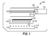
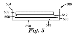
- 光入力表面と光出力表面とを有する光透過性プレートと、
前記光透過性プレートの、前記光入力表面又は光出力表面の少なくとも一方を覆う内側及び外側表面を有するカバーフィルムと、
前記カバーフィルムの前記外側表面に隣接するか又は付着された第1の光学フィルムと、
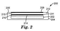
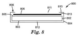
を備える光管理アセンブリ。 - 光入力表面と光出力表面とを有する光透過性プレートと、
前記光透過性プレートの、前記光入力表面又は光出力表面の少なくとも一方を覆うカバーフィルムと、
前記カバーフィルムと前記光透過性プレートとの間の第1の光学フィルムと、
を備え、
前記光透過性プレート及び前記光学フィルムがそれぞれ主要対向表面を有し、前記光透過性プレートの前記主要対向表面又は前記光学フィルムの前記主要対向表面の少なくとも一方が構造化表面である、
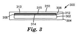
光管理アセンブリ。 - 光入力表面と光出力表面とを有する光透過性プレートと、
前記光透過性プレートの、前記光入力表面又は光出力表面の少なくとも一方を覆う内側及び外側表面を有するカバーフィルムと、
前記光透過性プレートの前記光入力表面又は光出力表面のいずれかに隣接し、カバーフィルム枠及び開口部を画定する、前記カバーフィルム内の窓と、
前記カバーフィルム枠と前記光透過性プレートとの間に配置された第1の光学フィルムと、
を備える光管理アセンブリ。 - 前記光透過性プレートが、構造化された光出力表面を有する、請求項1〜3のいずれか一項に記載の光管理アセンブリ。
- 前記構造化表面が艶消し表面である、請求項4に記載の光管理アセンブリ。
- 前記カバーフィルムが前記光透過性プレートを封入する、請求項1〜3のいずれか一項に記載の光管理アセンブリ。
- 前記光学フィルムが反射型偏光子又は吸収型偏光子である、請求項1〜3のいずれか一項に記載の光管理アセンブリ。
- 前記カバーフィルムが、ポリオレフィン、ポリエステル、ポリカーボネート、アクリル、又はポリスチレンを含む、請求項1〜3のいずれか一項に記載の光管理アセンブリ。
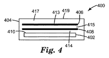
- 前記カバーフィルムが熱収縮性である、請求項8に記載の光管理アセンブリ。
- 前記光透過性プレートと前記カバーフィルムとの間の第2の光学フィルムを更に備える、請求項1に記載の光管理アセンブリ。
- 前記第2の光学フィルムが、前記光透過性プレートの光出力表面と前記カバーフィルムの光入力表面との間にある、請求項10に記載の光管理アセンブリ。
- 前記光学フィルムが、光入力表面でもある前記カバーフィルムの前記外側表面に隣接する、請求項1に記載の光管理アセンブリ。
- 前記第1の光学フィルムの少なくとも外側表面を覆う第2のカバーフィルムを更に備える、請求項1に記載の光管理アセンブリ。
- 前記第2のカバーフィルムが、前記第1の光学フィルム及び前記第1のカバーフィルムを封入する、請求項13に記載の光管理アセンブリ。
- 前記カバーフィルムが、前記光透過性プレートの前記入力表面を覆い、前記光管理アセンブリが、前記光透過性プレートの前記入力表面を覆う前記カバーフィルムの前記外側表面に隣接するか又は付着された第2の光学フィルムを更に備える、請求項1に記載の光管理アセンブリ。
- 前記開口部が表示画面を画定する、請求項3に記載の光管理アセンブリ。
- 前記光学フィルムが、前記カバーフィルム枠と前記光透過性プレートの前記出力表面との間にある、請求項3に記載の光管理アセンブリ。
Applications Claiming Priority (2)
| Application Number | Priority Date | Filing Date | Title |
|---|---|---|---|
| US11/832,066 US20090034268A1 (en) | 2007-08-01 | 2007-08-01 | Light management assembly |
| PCT/US2008/068485 WO2009017913A2 (en) | 2007-08-01 | 2008-06-27 | Light management assembly |
Publications (2)
| Publication Number | Publication Date |
|---|---|
| JP2010535359A true JP2010535359A (ja) | 2010-11-18 |
| JP2010535359A5 JP2010535359A5 (ja) | 2011-08-11 |
Family
ID=40305163
Family Applications (1)
| Application Number | Title | Priority Date | Filing Date |
|---|---|---|---|
| JP2010520029A Pending JP2010535359A (ja) | 2007-08-01 | 2008-06-27 | 光管理アセンブリ |
Country Status (7)
| Country | Link |
|---|---|
| US (2) | US20090034268A1 (ja) |
| EP (1) | EP2174184A4 (ja) |
| JP (1) | JP2010535359A (ja) |
| KR (1) | KR20100051826A (ja) |
| CN (1) | CN101772728B (ja) |
| TW (1) | TWI463215B (ja) |
| WO (1) | WO2009017913A2 (ja) |
Cited By (1)
| Publication number | Priority date | Publication date | Assignee | Title |
|---|---|---|---|---|
| JP2016508624A (ja) * | 2013-02-20 | 2016-03-22 | エルジー・ケム・リミテッド | ディスプレイ装置用パッケージングフィルム |
Families Citing this family (5)
| Publication number | Priority date | Publication date | Assignee | Title |
|---|---|---|---|---|
| US20250075868A1 (en) * | 2013-01-30 | 2025-03-06 | Cree Lighting Usa Llc | Lighting Devices Having Optical Waveguides for Controlled Light Distribution |
| KR20150038876A (ko) * | 2013-10-01 | 2015-04-09 | 삼성디스플레이 주식회사 | 액정 표시 장치 |
| CN107110434B (zh) * | 2014-12-18 | 2020-07-24 | 三菱电机株式会社 | 灯、灯用波长辨别罩、照明装置以及灯的制造方法 |
| TWI595279B (zh) * | 2015-10-13 | 2017-08-11 | 元太科技工業股份有限公司 | 反射式顯示裝置與其前光模組 |
| CN115042499A (zh) * | 2022-07-18 | 2022-09-13 | 中航华东光电有限公司 | 新型多合一光学膜制作方法 |
Citations (5)
| Publication number | Priority date | Publication date | Assignee | Title |
|---|---|---|---|---|
| JPS51153648U (ja) * | 1975-05-30 | 1976-12-08 | ||
| JP2001272509A (ja) * | 2000-03-24 | 2001-10-05 | Advanced Display Inc | 光拡散材および該光拡散材を用いる液晶表示装置 |
| JP2003249108A (ja) * | 2002-02-25 | 2003-09-05 | Fujitsu Display Technologies Corp | バックライト装置及び光学シート体及び液晶表示装置 |
| JP2005317411A (ja) * | 2004-04-30 | 2005-11-10 | Sharp Corp | バックライト装置 |
| JP2007155934A (ja) * | 2005-12-01 | 2007-06-21 | Fujifilm Corp | ディスプレイ用光学シート |
Family Cites Families (27)
| Publication number | Priority date | Publication date | Assignee | Title |
|---|---|---|---|---|
| US5056892A (en) * | 1985-11-21 | 1991-10-15 | Minnesota Mining And Manufacturing Company | Totally internally reflecting thin, flexible film |
| TW289095B (ja) * | 1993-01-11 | 1996-10-21 | ||
| US5882774A (en) * | 1993-12-21 | 1999-03-16 | Minnesota Mining And Manufacturing Company | Optical film |
| US5751388A (en) * | 1995-04-07 | 1998-05-12 | Honeywell Inc. | High efficiency polarized display |
| US5867316A (en) * | 1996-02-29 | 1999-02-02 | Minnesota Mining And Manufacturing Company | Multilayer film having a continuous and disperse phase |
| US5825543A (en) * | 1996-02-29 | 1998-10-20 | Minnesota Mining And Manufacturing Company | Diffusely reflecting polarizing element including a first birefringent phase and a second phase |
| US6497946B1 (en) * | 1997-10-24 | 2002-12-24 | 3M Innovative Properties Company | Diffuse reflective articles |
| JPH11259021A (ja) * | 1998-02-17 | 1999-09-24 | Internatl Business Mach Corp <Ibm> | 液晶表示パネルおよび液晶表示装置 |
| US6322236B1 (en) * | 1999-02-09 | 2001-11-27 | 3M Innovative Properties Company | Optical film with defect-reducing surface and method for making same |
| US6122103A (en) * | 1999-06-22 | 2000-09-19 | Moxtech | Broadband wire grid polarizer for the visible spectrum |
| US6352748B1 (en) * | 2000-03-22 | 2002-03-05 | Eastman Kodak Company | Imaging element including brace and mechanical holding means |
| US6917399B2 (en) * | 2001-02-22 | 2005-07-12 | 3M Innovative Properties Company | Optical bodies containing cholesteric liquid crystal material and methods of manufacture |
| US7010212B2 (en) * | 2002-05-28 | 2006-03-07 | 3M Innovative Properties Company | Multifunctional optical assembly |
| JP3873835B2 (ja) * | 2002-07-22 | 2007-01-31 | セイコーエプソン株式会社 | 液晶表示装置及び電子機器 |
| JP4424904B2 (ja) * | 2002-12-02 | 2010-03-03 | スリーエム イノベイティブ プロパティズ カンパニー | シート状光学要素パッケージ体の製造方法及び製造装置 |
| US7314652B2 (en) * | 2003-02-28 | 2008-01-01 | General Electric Company | Diffuser for flat panel display |
| US7413336B2 (en) * | 2003-08-29 | 2008-08-19 | 3M Innovative Properties Company | Adhesive stacking for multiple optical films |
| US7710511B2 (en) * | 2004-10-15 | 2010-05-04 | 3M Innovative Properties Company | Liquid crystal displays with laminated diffuser plates |
| US7446827B2 (en) * | 2004-10-15 | 2008-11-04 | 3M Innovative Properties Company | Direct-lit liquid crystal displays with laminated diffuser plates |
| US7339635B2 (en) * | 2005-01-14 | 2008-03-04 | 3M Innovative Properties Company | Pre-stacked optical films with adhesive layer |
| US20060257678A1 (en) * | 2005-05-10 | 2006-11-16 | Benson Olester Jr | Fiber reinforced optical films |
| US20070030415A1 (en) * | 2005-05-16 | 2007-02-08 | Epstein Kenneth A | Back-lit displays with high illumination uniformity |
| US7319246B2 (en) * | 2005-06-23 | 2008-01-15 | Lumination Llc | Luminescent sheet covering for LEDs |
| KR20080045751A (ko) * | 2005-09-12 | 2008-05-23 | 후지필름 가부시키가이샤 | 디스플레이용 광학 시트, 그 제조 방법, 및 포장 방법 |
| TWI274938B (en) * | 2005-10-28 | 2007-03-01 | Chung Shan Inst Of Science | Fabricating method of liquid crystal panel |
| US20070139574A1 (en) * | 2005-12-19 | 2007-06-21 | Byung-Soo Ko | Plateless LCD Unit |
| JP4175433B2 (ja) * | 2007-02-09 | 2008-11-05 | ソニー株式会社 | 光学素子包装体、バックライトおよび液晶表示装置 |
-
2007
- 2007-08-01 US US11/832,066 patent/US20090034268A1/en active Pending
-
2008
- 2008-06-27 EP EP08772117A patent/EP2174184A4/en not_active Withdrawn
- 2008-06-27 US US12/670,143 patent/US20110051392A1/en not_active Abandoned
- 2008-06-27 KR KR1020107004130A patent/KR20100051826A/ko not_active Ceased
- 2008-06-27 CN CN2008801014292A patent/CN101772728B/zh not_active Expired - Fee Related
- 2008-06-27 JP JP2010520029A patent/JP2010535359A/ja active Pending
- 2008-06-27 WO PCT/US2008/068485 patent/WO2009017913A2/en not_active Ceased
- 2008-07-10 TW TW097126118A patent/TWI463215B/zh not_active IP Right Cessation
Patent Citations (5)
| Publication number | Priority date | Publication date | Assignee | Title |
|---|---|---|---|---|
| JPS51153648U (ja) * | 1975-05-30 | 1976-12-08 | ||
| JP2001272509A (ja) * | 2000-03-24 | 2001-10-05 | Advanced Display Inc | 光拡散材および該光拡散材を用いる液晶表示装置 |
| JP2003249108A (ja) * | 2002-02-25 | 2003-09-05 | Fujitsu Display Technologies Corp | バックライト装置及び光学シート体及び液晶表示装置 |
| JP2005317411A (ja) * | 2004-04-30 | 2005-11-10 | Sharp Corp | バックライト装置 |
| JP2007155934A (ja) * | 2005-12-01 | 2007-06-21 | Fujifilm Corp | ディスプレイ用光学シート |
Cited By (2)
| Publication number | Priority date | Publication date | Assignee | Title |
|---|---|---|---|---|
| JP2016508624A (ja) * | 2013-02-20 | 2016-03-22 | エルジー・ケム・リミテッド | ディスプレイ装置用パッケージングフィルム |
| US9720267B2 (en) | 2013-02-20 | 2017-08-01 | Lg Chem, Ltd. | Display device |
Also Published As
| Publication number | Publication date |
|---|---|
| TWI463215B (zh) | 2014-12-01 |
| EP2174184A4 (en) | 2010-08-11 |
| KR20100051826A (ko) | 2010-05-18 |
| EP2174184A2 (en) | 2010-04-14 |
| US20090034268A1 (en) | 2009-02-05 |
| CN101772728B (zh) | 2012-03-21 |
| US20110051392A1 (en) | 2011-03-03 |
| CN101772728A (zh) | 2010-07-07 |
| WO2009017913A3 (en) | 2009-03-19 |
| TW200912461A (en) | 2009-03-16 |
| WO2009017913A2 (en) | 2009-02-05 |
Similar Documents
| Publication | Publication Date | Title |
|---|---|---|
| JP4175433B2 (ja) | 光学素子包装体、バックライトおよび液晶表示装置 | |
| JP5475232B2 (ja) | 複合ディフューザプレート、およびそれらを使用する直接照明液晶ディスプレイ | |
| JP5319116B2 (ja) | 積層ディフューザープレートを備えた液晶ディスプレイ | |
| US7446827B2 (en) | Direct-lit liquid crystal displays with laminated diffuser plates | |
| JP4175431B1 (ja) | 光学素子包装体、バックライトおよび液晶表示装置 | |
| US20090310060A1 (en) | Optical package, method of manufacturing the same, backlight, and liquid crystal display | |
| US20110103036A1 (en) | Optical film | |
| JP2009134251A (ja) | 拘束された非対称拡散体を備える光学素子 | |
| WO2007067603A1 (en) | Diffuse multilayer optical assembly | |
| JP2009524112A (ja) | ディスプレイシステム用光管理フィルムパッケージ及びこれを用いるシステム | |
| JP2010535359A (ja) | 光管理アセンブリ | |
| CN101392884A (zh) | 光学元件封装体、背光和液晶显示器 | |
| KR101585000B1 (ko) | 액정표시장치 | |
| JP2008250327A (ja) | 包装体およびその製造方法、バックライト、ならびに液晶表示装置 | |
| JP2008261961A (ja) | 光学素子包装体、バックライトおよび液晶表示装置 | |
| JP2008197398A (ja) | 光学素子包装体、バックライトおよび液晶表示装置 | |
| JP2008261959A (ja) | 光学素子包括体、バックライトおよび液晶表示装置 | |
| JP2009075573A (ja) | 光学素子包装体、バックライトおよび液晶表示装置 |
Legal Events
| Date | Code | Title | Description |
|---|---|---|---|
| A521 | Request for written amendment filed |
Free format text: JAPANESE INTERMEDIATE CODE: A523 Effective date: 20110623 |
|
| A621 | Written request for application examination |
Free format text: JAPANESE INTERMEDIATE CODE: A621 Effective date: 20110623 |
|
| A977 | Report on retrieval |
Free format text: JAPANESE INTERMEDIATE CODE: A971007 Effective date: 20130204 |
|
| A131 | Notification of reasons for refusal |
Free format text: JAPANESE INTERMEDIATE CODE: A131 Effective date: 20130305 |
|
| A521 | Request for written amendment filed |
Free format text: JAPANESE INTERMEDIATE CODE: A523 Effective date: 20130604 |
|
| A02 | Decision of refusal |
Free format text: JAPANESE INTERMEDIATE CODE: A02 Effective date: 20130806 |
|
| A521 | Request for written amendment filed |
Free format text: JAPANESE INTERMEDIATE CODE: A523 Effective date: 20131204 |
|
| A911 | Transfer to examiner for re-examination before appeal (zenchi) |
Free format text: JAPANESE INTERMEDIATE CODE: A911 Effective date: 20131211 |
|
| A912 | Re-examination (zenchi) completed and case transferred to appeal board |
Free format text: JAPANESE INTERMEDIATE CODE: A912 Effective date: 20140110 |