JP2010534860A - 非線形応用のために最適化されたフォトニック禁制帯および全反射による導光用のハイブリッド微細構造光ファイバ - Google Patents
非線形応用のために最適化されたフォトニック禁制帯および全反射による導光用のハイブリッド微細構造光ファイバ Download PDFInfo
- Publication number
- JP2010534860A JP2010534860A JP2010517454A JP2010517454A JP2010534860A JP 2010534860 A JP2010534860 A JP 2010534860A JP 2010517454 A JP2010517454 A JP 2010517454A JP 2010517454 A JP2010517454 A JP 2010517454A JP 2010534860 A JP2010534860 A JP 2010534860A
- Authority
- JP
- Japan
- Prior art keywords
- refractive index
- optical fiber
- inclusions
- rti
- fundamental mode
- Prior art date
- Legal status (The legal status is an assumption and is not a legal conclusion. Google has not performed a legal analysis and makes no representation as to the accuracy of the status listed.)
- Ceased
Links
- 239000013307 optical fiber Substances 0.000 title claims abstract description 95
- 239000000463 material Substances 0.000 claims abstract description 51
- 238000005253 cladding Methods 0.000 claims abstract description 40
- VYPSYNLAJGMNEJ-UHFFFAOYSA-N Silicium dioxide Chemical compound O=[Si]=O VYPSYNLAJGMNEJ-UHFFFAOYSA-N 0.000 claims description 102
- 239000000377 silicon dioxide Substances 0.000 claims description 50
- 239000000835 fiber Substances 0.000 claims description 35
- 230000000737 periodic effect Effects 0.000 claims description 19
- 238000000034 method Methods 0.000 claims description 5
- 230000009022 nonlinear effect Effects 0.000 claims description 5
- 230000001747 exhibiting effect Effects 0.000 claims description 4
- 239000011521 glass Substances 0.000 claims description 4
- 239000007788 liquid Substances 0.000 claims description 4
- 230000001902 propagating effect Effects 0.000 claims description 4
- 239000005387 chalcogenide glass Substances 0.000 claims description 3
- SITVSCPRJNYAGV-UHFFFAOYSA-L tellurite Chemical compound [O-][Te]([O-])=O SITVSCPRJNYAGV-UHFFFAOYSA-L 0.000 claims description 3
- 238000010586 diagram Methods 0.000 description 14
- 238000004364 calculation method Methods 0.000 description 10
- 230000007547 defect Effects 0.000 description 7
- 229910052732 germanium Inorganic materials 0.000 description 7
- GNPVGFCGXDBREM-UHFFFAOYSA-N germanium atom Chemical compound [Ge] GNPVGFCGXDBREM-UHFFFAOYSA-N 0.000 description 7
- 230000007246 mechanism Effects 0.000 description 6
- 239000013078 crystal Substances 0.000 description 5
- 230000009021 linear effect Effects 0.000 description 5
- 235000012239 silicon dioxide Nutrition 0.000 description 5
- 230000003287 optical effect Effects 0.000 description 4
- 239000006185 dispersion Substances 0.000 description 3
- YBMRDBCBODYGJE-UHFFFAOYSA-N germanium dioxide Chemical compound O=[Ge]=O YBMRDBCBODYGJE-UHFFFAOYSA-N 0.000 description 3
- LFQSCWFLJHTTHZ-UHFFFAOYSA-N Ethanol Chemical compound CCO LFQSCWFLJHTTHZ-UHFFFAOYSA-N 0.000 description 2
- 241000961787 Josa Species 0.000 description 2
- 239000012530 fluid Substances 0.000 description 2
- 239000005350 fused silica glass Substances 0.000 description 2
- 239000004038 photonic crystal Substances 0.000 description 2
- PXGOKWXKJXAPGV-UHFFFAOYSA-N Fluorine Chemical compound FF PXGOKWXKJXAPGV-UHFFFAOYSA-N 0.000 description 1
- BPQQTUXANYXVAA-UHFFFAOYSA-N Orthosilicate Chemical compound [O-][Si]([O-])([O-])[O-] BPQQTUXANYXVAA-UHFFFAOYSA-N 0.000 description 1
- OAICVXFJPJFONN-UHFFFAOYSA-N Phosphorus Chemical compound [P] OAICVXFJPJFONN-UHFFFAOYSA-N 0.000 description 1
- GWEVSGVZZGPLCZ-UHFFFAOYSA-N Titan oxide Chemical compound O=[Ti]=O GWEVSGVZZGPLCZ-UHFFFAOYSA-N 0.000 description 1
- 238000010521 absorption reaction Methods 0.000 description 1
- 230000008859 change Effects 0.000 description 1
- 239000000470 constituent Substances 0.000 description 1
- 238000010276 construction Methods 0.000 description 1
- 230000008878 coupling Effects 0.000 description 1
- 238000010168 coupling process Methods 0.000 description 1
- 238000005859 coupling reaction Methods 0.000 description 1
- 230000001627 detrimental effect Effects 0.000 description 1
- 238000004134 energy conservation Methods 0.000 description 1
- 229910052731 fluorine Inorganic materials 0.000 description 1
- 239000011737 fluorine Substances 0.000 description 1
- 238000003780 insertion Methods 0.000 description 1
- 230000037431 insertion Effects 0.000 description 1
- 230000003993 interaction Effects 0.000 description 1
- 230000002093 peripheral effect Effects 0.000 description 1
- 229910052698 phosphorus Inorganic materials 0.000 description 1
- 239000011574 phosphorus Substances 0.000 description 1
- 238000004321 preservation Methods 0.000 description 1
- NTHWMYGWWRZVTN-UHFFFAOYSA-N sodium silicate Chemical compound [Na+].[Na+].[O-][Si]([O-])=O NTHWMYGWWRZVTN-UHFFFAOYSA-N 0.000 description 1
- 230000003595 spectral effect Effects 0.000 description 1
- XLYOFNOQVPJJNP-UHFFFAOYSA-N water Substances O XLYOFNOQVPJJNP-UHFFFAOYSA-N 0.000 description 1
Images


Classifications
-
- G—PHYSICS
- G02—OPTICS
- G02B—OPTICAL ELEMENTS, SYSTEMS OR APPARATUS
- G02B6/00—Light guides; Structural details of arrangements comprising light guides and other optical elements, e.g. couplings
- G02B6/02—Optical fibres with cladding with or without a coating
- G02B6/02295—Microstructured optical fibre
- G02B6/02314—Plurality of longitudinal structures extending along optical fibre axis, e.g. holes
- G02B6/02342—Plurality of longitudinal structures extending along optical fibre axis, e.g. holes characterised by cladding features, i.e. light confining region
- G02B6/02347—Longitudinal structures arranged to form a regular periodic lattice, e.g. triangular, square, honeycomb unit cell repeated throughout cladding
- G02B6/02352—Complex periodic lattices or multiple interpenetrating periodic lattices, e.g. unit cell having more than two materials, partially internally coated holes, for multiple bandgaps
-
- G—PHYSICS
- G02—OPTICS
- G02F—OPTICAL DEVICES OR ARRANGEMENTS FOR THE CONTROL OF LIGHT BY MODIFICATION OF THE OPTICAL PROPERTIES OF THE MEDIA OF THE ELEMENTS INVOLVED THEREIN; NON-LINEAR OPTICS; FREQUENCY-CHANGING OF LIGHT; OPTICAL LOGIC ELEMENTS; OPTICAL ANALOGUE/DIGITAL CONVERTERS
- G02F1/00—Devices or arrangements for the control of the intensity, colour, phase, polarisation or direction of light arriving from an independent light source, e.g. switching, gating or modulating; Non-linear optics
- G02F1/35—Non-linear optics
- G02F1/365—Non-linear optics in an optical waveguide structure
-
- G—PHYSICS
- G02—OPTICS
- G02B—OPTICAL ELEMENTS, SYSTEMS OR APPARATUS
- G02B6/00—Light guides; Structural details of arrangements comprising light guides and other optical elements, e.g. couplings
- G02B6/02—Optical fibres with cladding with or without a coating
- G02B6/02295—Microstructured optical fibre
- G02B6/02314—Plurality of longitudinal structures extending along optical fibre axis, e.g. holes
- G02B6/02342—Plurality of longitudinal structures extending along optical fibre axis, e.g. holes characterised by cladding features, i.e. light confining region
- G02B6/02371—Cross section of longitudinal structures is non-circular
-
- G—PHYSICS
- G02—OPTICS
- G02B—OPTICAL ELEMENTS, SYSTEMS OR APPARATUS
- G02B6/00—Light guides; Structural details of arrangements comprising light guides and other optical elements, e.g. couplings
- G02B6/02—Optical fibres with cladding with or without a coating
- G02B6/02295—Microstructured optical fibre
- G02B6/02314—Plurality of longitudinal structures extending along optical fibre axis, e.g. holes
- G02B6/02342—Plurality of longitudinal structures extending along optical fibre axis, e.g. holes characterised by cladding features, i.e. light confining region
- G02B6/0238—Longitudinal structures having higher refractive index than background material, e.g. high index solid rods
-
- G—PHYSICS
- G02—OPTICS
- G02B—OPTICAL ELEMENTS, SYSTEMS OR APPARATUS
- G02B6/00—Light guides; Structural details of arrangements comprising light guides and other optical elements, e.g. couplings
- G02B6/02—Optical fibres with cladding with or without a coating
- G02B6/02295—Microstructured optical fibre
- G02B6/02314—Plurality of longitudinal structures extending along optical fibre axis, e.g. holes
- G02B6/02385—Comprising liquid, e.g. fluid filled holes
-
- G—PHYSICS
- G02—OPTICS
- G02F—OPTICAL DEVICES OR ARRANGEMENTS FOR THE CONTROL OF LIGHT BY MODIFICATION OF THE OPTICAL PROPERTIES OF THE MEDIA OF THE ELEMENTS INVOLVED THEREIN; NON-LINEAR OPTICS; FREQUENCY-CHANGING OF LIGHT; OPTICAL LOGIC ELEMENTS; OPTICAL ANALOGUE/DIGITAL CONVERTERS
- G02F1/00—Devices or arrangements for the control of the intensity, colour, phase, polarisation or direction of light arriving from an independent light source, e.g. switching, gating or modulating; Non-linear optics
- G02F1/35—Non-linear optics
- G02F1/353—Frequency conversion, i.e. wherein a light beam is generated with frequency components different from those of the incident light beams
-
- G—PHYSICS
- G02—OPTICS
- G02F—OPTICAL DEVICES OR ARRANGEMENTS FOR THE CONTROL OF LIGHT BY MODIFICATION OF THE OPTICAL PROPERTIES OF THE MEDIA OF THE ELEMENTS INVOLVED THEREIN; NON-LINEAR OPTICS; FREQUENCY-CHANGING OF LIGHT; OPTICAL LOGIC ELEMENTS; OPTICAL ANALOGUE/DIGITAL CONVERTERS
- G02F1/00—Devices or arrangements for the control of the intensity, colour, phase, polarisation or direction of light arriving from an independent light source, e.g. switching, gating or modulating; Non-linear optics
- G02F1/35—Non-linear optics
- G02F1/37—Non-linear optics for second-harmonic generation
- G02F1/377—Non-linear optics for second-harmonic generation in an optical waveguide structure
- G02F1/383—Non-linear optics for second-harmonic generation in an optical waveguide structure of the optical fibre type
-
- G—PHYSICS
- G02—OPTICS
- G02F—OPTICAL DEVICES OR ARRANGEMENTS FOR THE CONTROL OF LIGHT BY MODIFICATION OF THE OPTICAL PROPERTIES OF THE MEDIA OF THE ELEMENTS INVOLVED THEREIN; NON-LINEAR OPTICS; FREQUENCY-CHANGING OF LIGHT; OPTICAL LOGIC ELEMENTS; OPTICAL ANALOGUE/DIGITAL CONVERTERS
- G02F2202/00—Materials and properties
- G02F2202/32—Photonic crystals
Landscapes
- Physics & Mathematics (AREA)
- Nonlinear Science (AREA)
- General Physics & Mathematics (AREA)
- Optics & Photonics (AREA)
- Glass Compositions (AREA)
- Optical Fibers, Optical Fiber Cores, And Optical Fiber Bundles (AREA)
- Optical Couplings Of Light Guides (AREA)
Abstract
【選択図】図1
Description
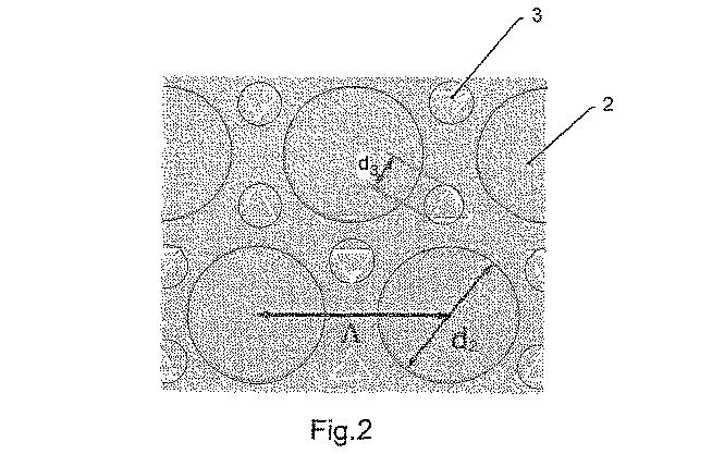
d2/Λ=0.725
ここで:
‐d2は介在物2の直径であり、
‐Λは介在物2の2つの中心間の距離(ネットワークステップ)である。
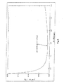
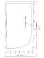
図5〜7のフォトニック禁制帯の図表は、図1の断面構造を含むが、介在物の周期的ネットワークに中央の欠陥4の無い光ファイバに対して計算されたものである。さらに、これらの図5〜7には、フォトニック禁制帯(BG1、BG2、BG3等)に加えて、光ファイバのクラッドの平均実効屈折率(すなわち、屈折率n3およびn2の介在物の周期的ネットワークを特徴とするクラッドの微細構造材料に対応する均質な材料が有する平均屈折率)の変動が、正規化された波長(λ/Λ)の関数として描かれている。計算は、シリカの屈折率が一定であり1.45と想定されることを追加的前提として実現されている。
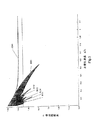
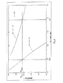
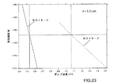
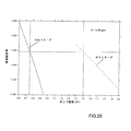
図1および図2に係る光ファイバ(ゲルマニウムをドープした介在物2および空気孔によって形成される介在物3を持つ)について、第1フォトニック禁制帯(BG1)および全反射帯(RTI)における基本モードの実効屈折率(n)の展開を、介在物のネットワークの様々なステップ(Λ)値に対して計算した。これらの計算の結果は、図8〜12の曲線に対応する。屈折率n1は、セルマイヤの法則に従って展開する。介在物のネットワークのステップ(Λ)の値は次の通りであった。
図8:Λ=0.798μm
図9:Λ=1.386μm
図10:Λ=1.785μm
図11:Λ=0.588μm
図12:Λ=0.92μm
(i)2つの異なる波長λBG1およびλRTIで、
(ii)クラッド1の背景材の屈折率より低い実効屈折率(n)値に対し、
基本モードの屈折率(n)の均一性を有することが可能であることを示している。
図8:λBG1=0.4μmおよびλRTI=0.8μm(周波数の2倍化)
図9:λBG1=0.59μmおよびλRTI=1.18μm(周波数の2倍化)
図10:λBG1=0.75μmおよびλRTI=1.5μm(周波数の2倍化)
図11:λBG1=0.354μmおよびλRTI=1.064μm(周波数の3倍化)
図12:λBG1=0.5μmおよびλRTI=1.5μm(周波数の3倍化)
d2/Λ=d3/Λ=0.4
Λn=32×10−3
図18:Λ=1.79μm
図19:Λ=2.06μm
図20:Λ=2.67μm
d2/Λ=0.72;d3/Λ=0.32
Λn=30×10−3
図23:Λ=1.22μm
図24:Λ=1.42μm
図25:Λ=1.86μm
Claims (26)
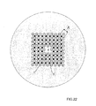
- 屈折率(n1)を有する背景材および少なくとも2種類の複数の介在物を備えたクラッド(1)の第1タイプの介在物(2)が前記背景材の屈折率(n1)より高い屈折率(n2)を有し、第2タイプの介在物(3)が前記背景材の屈折率(n1)より低い屈折率(n3)を有して成るクラッド(1)に包囲されたコア(4)を含み、光の基本モードのフォトニック禁制帯による導光を可能にする微細構造光ファイバであって、前記クラッドの介在物(2、3)が、波長λRTIを中心とする光の基本モードの全反射(RTI)による導光を可能にし、かつ全反射(RTI)によって導光される基本モードのこのλRTIより低い波長λBG1を中心とする第1フォトニック禁制帯(BG1)での光の基本モードの導光を可能にするように、配列されかつ大きさを決定されることを特徴とする微細構造光ファイバ。
- 前記クラッド(1)の平均実効屈折率(nfsm)が、少なくとも波長λBG1より高い波長範囲では前記クラッド(1)の前記背景材の屈折率(n1)より低いことを特徴とする、請求項1に記載の微細構造光ファイバ。
- 前記コア(4)が前記第1タイプの介在物(2)によって構成される中央クラウンによって包囲され、前記第2タイプの全ての介在物(3)がこの中央クラウンの外側に位置されることを特徴とする、請求項1または2のいずれか1項に記載の微細構造光ファイバ。
- 前記介在物(2)の屈折率(n2)が前記コア(4)の屈折率(n4)より高いことを特徴とする、請求項1〜3のいずれか1項に記載の微細構造光ファイバ。
- 前記ファイバの前記コア(4)が前記クラッド(1)と同じ背景材を含むことを特徴とする、請求項1〜4のいずれか1項に記載の微細構造光ファイバ。
- 前記コア(4)の屈折率(n4)が前記クラッド(1)の前記背景材の屈折率(n1)と等しいことを特徴とする、請求項1〜5のいずれか1項に記載の微細構造光ファイバ。
- 前記ファイバの前記コア(4)が前記クラッド(1)の前記背景材と同一材料から構成されることを特徴とする、請求項6に記載の微細構造光ファイバ。
- 前記介在物(2、3)が、一定ステップ(Λ)によって特徴付けられる周期的ネットワークの形状に配列されることを特徴とする、請求項1〜7のいずれか1項に記載の微細構造光ファイバ。
- 前記クラッド(1)の平均実効屈折率(nfsm)が少なくとも波長λBG1より高い波長範囲では前記クラッド(1)の前記背景材の屈折率(n1)より低くなるように、前記第2タイプの介在物(3)の大きさおよび介在物のネットワークのステップ(Λ)が選択されることを特徴とする、請求項8に記載の微細構造光ファイバ。
- 前記クラッドの前記介在物(2、3)が、位相整合されたm個の波(m≧3)の組合せを可能にするような仕方で配列されかつ大きさを決定され、これらの波のうちの少なくとも2つが異なる波長(λRTI、λBG1)を有し、それぞれ全反射(RTI)によって導光される基本モードおよび第1フォトニック禁制帯(BG1)で導光される基本モードに属することを特徴とする、請求項1〜9のいずれか1項に記載の微細構造光ファイバ。
- 第1禁止帯(BG2)で導光される基本モードおよび全反射(RTI)によって導光される基本モードが次の条件(a)および(b)、すなわち
を累積的に順守し、mが3以上の整数であり、nλiが波長λiで光ファイバを伝搬する基本モードの実効屈折率の値であること、ならびに
前記条件(a)および(b)を順守する波長λiのうち、少なくとも1つの波長(λRTI)が全反射(RTI)によって導光される基本モードに属し、少なくとも1つの波長(λBG1)が第1禁止帯(BG1)で導光される基本モードに属することを特徴とする、請求項1〜10のいずれか1項に記載の微細構造光ファイバ。 - 全反射(RTI)によって導光される基本モードおよび第1フォトニック禁制帯(BG1)で導光される基本モードにそれぞれ属する少なくとも2つの異なる波長λRTIおよびλBG1に対し、これら2つの波長λRTIおよびλBG1におけるファイバの実効屈折率(nλRTI;nλBG1)が等しくかつ前記クラッドの前記背景材の屈折率(n1)より低くなるように、前記クラッドの前記介在物(2、3)が配列されかつ大きさを決定されることを特徴とする、請求項1〜10のいずれか1項に記載の微細構造光ファイバ。
- 前記2つの波長λRTIおよびλBG1が次の条件、すなわちλRTI=k×λBG1(kは2以上の整数である)を順守することを特徴とする、請求項1〜12のいずれか1項に記載の微細構造光ファイバ。
- 前記2つの波長λRTIおよびλBG1が次の条件、すなわちλRTI=2λBG1を順守することを特徴とする、請求項13に記載の微細構造光ファイバ。
- 前記2つの波長λRTIおよびλBG1が次の条件、すなわちλRTI=3λBG1を順守することを特徴とする、請求項13に記載の微細構造光ファイバ。
- 全反射(RTI)によって導光される基本モードの波長λRTIが、第1禁制帯(BG1)で導光される基本モードの波長範囲の外側に位置されることを特徴とする、請求項1〜15のいずれか1項に記載の微細構造光ファイバ。
- 介在物(2、3)のネットワークが六角形であり、ハチの巣型であることを特徴とする、請求項1〜16のいずれか1項に記載の微細構造光ファイバ。
- 介在物(2、3)のネットワークが正方形を形成することを特徴とする、請求項1〜16のいずれか1項に記載の微細構造光ファイバ。
- 介在物(2、3)のネットワークが、前記第1タイプの介在物(2)によって形成される少なくとも2つの同心クラウンを含み、前記中央クラウンの前記第1タイプの介在物(2)を除いて、前記第1タイプの各介在物(2)が前記第2タイプの複数の介在物(3)によって包囲されることを特徴とする、請求項1〜18のいずれか1項に記載の微細構造光ファイバ。
- 前記クラッドの前記背景材がシリカから作られ、かつ前記第2タイプの介在物(3)が空気孔を含むことを特徴とする、請求項1〜19のいずれか1項に記載の微細構造光ファイバ。
- 前記クラッドの前記背景材がシリカから作られ、かつ前記第1タイプの介在物(2)がドープされたシリカの介在物を含むことを特徴とする、請求項1〜20のいずれか1項に記載の微細構造光ファイバ。
- 前記第1タイプの介在物(2)が、ゲルマニウムをドープされたシリカまたはリンをドープされたシリカから作られた介在物を含むことを特徴とする、請求項21に記載の微細構造光ファイバ。
- 前記クラッドの前記背景材がシリカから作られ、かつ前記第1タイプの介在物(2)がテルライトガラスまたはカルコゲナイドガラスから作られた介在物を含むことを特徴とする、請求項1〜22のいずれか1項に記載の微細構造光ファイバ。
- 前記第1タイプの介在物(2)が、前記クラッド(1)の背景材の屈折率(n1)より高い屈折率(n2)を呈する液体または気体を包含する介在物を含むことを特徴とする、請求項1〜23のいずれか1項に記載の微細構造光ファイバ。
- 前記第2タイプの介在物(3)が、前記クラッド(1)の背景材の屈折率(n1)より低い屈折率(n3)を呈する液体または気体を包含する介在物を含むことを特徴とする、請求項1〜24のいずれか1項に記載の微細構造光ファイバ。
- 非線形効果による周波数の発生のための、特に次の応用、すなわち双子の光子の発生、三つ子の光子の発生、複数の周波数の発生、特に周波数の2倍化および周波数の3倍化のうちの1つのための請求項1〜25のいずれか1項に記載の微細構造光ファイバの使用。
Applications Claiming Priority (2)
| Application Number | Priority Date | Filing Date | Title |
|---|---|---|---|
| EP07370013A EP2020611A1 (fr) | 2007-07-26 | 2007-07-26 | Fibre optique microstructurée hybride permettant un guidage par bandes interdites photoniques et par reflexion totale interne et optimisée pour des applications non linéaires |
| PCT/FR2008/001111 WO2009047404A1 (fr) | 2007-07-26 | 2008-07-25 | Fibre optique microstructuree hybride permettant un guidage par bandes interdites photoniques et par reflexion totale interne et optimisee pour des applications non lineaires |
Publications (2)
| Publication Number | Publication Date |
|---|---|
| JP2010534860A true JP2010534860A (ja) | 2010-11-11 |
| JP2010534860A5 JP2010534860A5 (ja) | 2011-08-18 |
Family
ID=38820120
Family Applications (1)
| Application Number | Title | Priority Date | Filing Date |
|---|---|---|---|
| JP2010517454A Ceased JP2010534860A (ja) | 2007-07-26 | 2008-07-25 | 非線形応用のために最適化されたフォトニック禁制帯および全反射による導光用のハイブリッド微細構造光ファイバ |
Country Status (4)
| Country | Link |
|---|---|
| US (1) | US8442372B2 (ja) |
| EP (2) | EP2020611A1 (ja) |
| JP (1) | JP2010534860A (ja) |
| WO (1) | WO2009047404A1 (ja) |
Families Citing this family (7)
| Publication number | Priority date | Publication date | Assignee | Title |
|---|---|---|---|---|
| EP3460543B1 (en) * | 2010-06-25 | 2021-07-21 | NKT Photonics A/S | Large core area single mode optical fiber |
| EP2533081A1 (en) * | 2011-06-09 | 2012-12-12 | Universite De Lille 1 Sciences Et Technologies | Hybrid photonic crystal fiber |
| CN108398781B (zh) * | 2018-03-12 | 2021-05-04 | 北京理工大学 | 一种模拟光纤激光自由空间相干合成能量分布的方法 |
| US11105973B2 (en) | 2019-01-11 | 2021-08-31 | Schott Corporation | Optically enhanced high resolution image guides |
| FR3102864B1 (fr) * | 2019-10-31 | 2021-11-12 | Univ Limoges | Architecture pour guide d’ondes électromagnétiques |
| EP4116747A1 (en) * | 2021-07-08 | 2023-01-11 | NKT Photonics A/S | Optical fiber |
| CN116259241A (zh) * | 2023-03-14 | 2023-06-13 | 京东方科技集团股份有限公司 | 一种显示面板及显示装置 |
-
2007
- 2007-07-26 EP EP07370013A patent/EP2020611A1/fr not_active Withdrawn
-
2008
- 2008-07-25 JP JP2010517454A patent/JP2010534860A/ja not_active Ceased
- 2008-07-25 WO PCT/FR2008/001111 patent/WO2009047404A1/fr not_active Ceased
- 2008-07-25 EP EP08837519A patent/EP2174171A1/fr not_active Withdrawn
- 2008-07-25 US US12/670,500 patent/US8442372B2/en not_active Expired - Fee Related
Non-Patent Citations (1)
| Title |
|---|
| JPN6013022878; CERQUEIRA A S JR ET AL: 'Hybrid photonic crystal fiber' OPTICS EXPRESS vol. 14, no. 2, 20060123, p.926-931 * |
Also Published As
| Publication number | Publication date |
|---|---|
| US8442372B2 (en) | 2013-05-14 |
| US20100226614A1 (en) | 2010-09-09 |
| EP2020611A1 (fr) | 2009-02-04 |
| EP2174171A1 (fr) | 2010-04-14 |
| WO2009047404A1 (fr) | 2009-04-16 |
Similar Documents
| Publication | Publication Date | Title |
|---|---|---|
| JP5674725B2 (ja) | 光ファイバ増幅器 | |
| Belardi et al. | Effect of core boundary curvature on the confinement losses of hollow antiresonant fibers | |
| JP4904241B2 (ja) | ホーリーファイバ | |
| JP2010534860A (ja) | 非線形応用のために最適化されたフォトニック禁制帯および全反射による導光用のハイブリッド微細構造光ファイバ | |
| JP5679420B2 (ja) | ソリッドフォトニックバンドギャップファイバおよび該ファイバを用いたファイバモジュールおよびファイバアンプ、ファイバレーザ | |
| EP2533081A1 (en) | Hybrid photonic crystal fiber | |
| JP4588113B2 (ja) | フォトニックバンドギャップファイバ | |
| Sharma et al. | Splicing of index-guiding microstructured optical fibers and single-mode fibers by controlled air-hole collapse: an analytical approach | |
| JPWO2008108404A1 (ja) | フォトニックバンドギャップファイバ | |
| Hao et al. | Optimized design of unsymmetrical gap nodeless hollow core fibers for optofluidic applications | |
| JP2010534860A5 (ja) | ||
| JP4130424B2 (ja) | 空孔アシスト光ファイバ | |
| Halder et al. | Design and numerical analysis of a modified core hexa–deca photonic crystal fiber for highly negative dispersion and birefringence control in optical communication bands | |
| JP2017503216A (ja) | 選択的に拡大された低屈折率の空間を備え、特に非線形効果の発生及び応力測定用の微細構造光ファイバ | |
| Akand et al. | Low loss hollow-core optical fibers conjoining tube lattice and revolver structures | |
| CN104020521A (zh) | 一种正方结构全固态带隙光纤 | |
| Kim et al. | Extremely high-Q quasi-BICs induced by simultaneously broken out-of-and in-plane symmetries in dielectric metasurfaces of low-index materials | |
| Yadav et al. | Quasi-periodic layering of linear/nonlinear materials in hollow core Bragg fiber for all-optical diode action | |
| Akand et al. | Low loss hollow core optical fibers combining lattice and negative curvature structures | |
| JP2011170173A (ja) | フォトニックバンドギャップファイバ | |
| Deng et al. | Low loss silicon microring resonator as comb filter | |
| Suzuki et al. | Design of dispersion-flattened photonic crystal fiber with 800 nm wide low-dispersion band | |
| Shaha et al. | Dual-Core Antiresonant Fiber Based Compact Broadband Polarization Beam Splitter | |
| Cheng et al. | Numerical simulation of dynamic bandgap control in all-solid chalcogenide–tellurite photonic bandgap fiber | |
| JP5160477B2 (ja) | 光ファイバ |
Legal Events
| Date | Code | Title | Description |
|---|---|---|---|
| A521 | Request for written amendment filed |
Free format text: JAPANESE INTERMEDIATE CODE: A523 Effective date: 20110629 |
|
| A621 | Written request for application examination |
Free format text: JAPANESE INTERMEDIATE CODE: A621 Effective date: 20110629 |
|
| A977 | Report on retrieval |
Free format text: JAPANESE INTERMEDIATE CODE: A971007 Effective date: 20130508 |
|
| A131 | Notification of reasons for refusal |
Free format text: JAPANESE INTERMEDIATE CODE: A131 Effective date: 20130517 |
|
| A521 | Request for written amendment filed |
Free format text: JAPANESE INTERMEDIATE CODE: A523 Effective date: 20130729 |
|
| A01 | Written decision to grant a patent or to grant a registration (utility model) |
Free format text: JAPANESE INTERMEDIATE CODE: A01 Effective date: 20140218 |
|
| A045 | Written measure of dismissal of application [lapsed due to lack of payment] |
Free format text: JAPANESE INTERMEDIATE CODE: A045 Effective date: 20140620 |