JP2010505247A - Photoelectric element - Google Patents
Photoelectric element Download PDFInfo
- Publication number
- JP2010505247A JP2010505247A JP2009529517A JP2009529517A JP2010505247A JP 2010505247 A JP2010505247 A JP 2010505247A JP 2009529517 A JP2009529517 A JP 2009529517A JP 2009529517 A JP2009529517 A JP 2009529517A JP 2010505247 A JP2010505247 A JP 2010505247A
- Authority
- JP
- Japan
- Prior art keywords
- layer
- spectrum
- electromagnetic radiation
- photoelectric
- photoelectric device
- Prior art date
- Legal status (The legal status is an assumption and is not a legal conclusion. Google has not performed a legal analysis and makes no representation as to the accuracy of the status listed.)
- Pending
Links
Images


Classifications
-
- H—ELECTRICITY
- H01—ELECTRIC ELEMENTS
- H01L—SEMICONDUCTOR DEVICES NOT COVERED BY CLASS H10
- H01L33/00—Semiconductor devices with at least one potential-jump barrier or surface barrier specially adapted for light emission; Processes or apparatus specially adapted for the manufacture or treatment thereof or of parts thereof; Details thereof
- H01L33/48—Semiconductor devices with at least one potential-jump barrier or surface barrier specially adapted for light emission; Processes or apparatus specially adapted for the manufacture or treatment thereof or of parts thereof; Details thereof characterised by the semiconductor body packages
- H01L33/50—Wavelength conversion elements
-
- H—ELECTRICITY
- H01—ELECTRIC ELEMENTS
- H01L—SEMICONDUCTOR DEVICES NOT COVERED BY CLASS H10
- H01L33/00—Semiconductor devices with at least one potential-jump barrier or surface barrier specially adapted for light emission; Processes or apparatus specially adapted for the manufacture or treatment thereof or of parts thereof; Details thereof
- H01L33/44—Semiconductor devices with at least one potential-jump barrier or surface barrier specially adapted for light emission; Processes or apparatus specially adapted for the manufacture or treatment thereof or of parts thereof; Details thereof characterised by the coatings, e.g. passivation layer or anti-reflective coating
-
- H—ELECTRICITY
- H01—ELECTRIC ELEMENTS
- H01L—SEMICONDUCTOR DEVICES NOT COVERED BY CLASS H10
- H01L33/00—Semiconductor devices with at least one potential-jump barrier or surface barrier specially adapted for light emission; Processes or apparatus specially adapted for the manufacture or treatment thereof or of parts thereof; Details thereof
- H01L33/48—Semiconductor devices with at least one potential-jump barrier or surface barrier specially adapted for light emission; Processes or apparatus specially adapted for the manufacture or treatment thereof or of parts thereof; Details thereof characterised by the semiconductor body packages
- H01L33/58—Optical field-shaping elements
Landscapes
- Engineering & Computer Science (AREA)
- Microelectronics & Electronic Packaging (AREA)
- Manufacturing & Machinery (AREA)
- Computer Hardware Design (AREA)
- Power Engineering (AREA)
- Led Device Packages (AREA)
- Optical Filters (AREA)
- Electroluminescent Light Sources (AREA)
Abstract
本発明は、オフ状態で所望の色印象を有する光電素子に関する。本発明によれば、光電素子は、駆動時に第1のスペクトルの電磁放射を放出する活性領域を含む半導体層列と、第1のスペクトルの電磁放射の光路で見て半導体層列の後方に配置され、第1のスペクトルの電磁放射の少なくとも一部を第2のスペクトルの電磁放射へ変換する波長変換層と、外部から当該の光電素子へ入射する放射の少なくとも一部を反射するフィルタ層とを有している。 The present invention relates to a photoelectric element having a desired color impression in an off state. According to the invention, the photoelectric element is disposed behind the semiconductor layer sequence as viewed in the optical path of the electromagnetic radiation of the first spectrum and the semiconductor layer sequence including an active region that emits the electromagnetic radiation of the first spectrum when driven. A wavelength converting layer that converts at least part of the electromagnetic radiation of the first spectrum into electromagnetic radiation of the second spectrum, and a filter layer that reflects at least part of the radiation incident on the photoelectric element from the outside Have.
Description
本願は独国出願第102006046199.1号に関連しており、その優先権を主張する。当該の出願の開示内容は本発明に関連する。 The present application is related to German patent application No. 102006046199.1 and claims its priority. The disclosure of that application is relevant to the present invention.
本発明は、駆動時に電磁放射を発光し、オフ状態で所望の色印象を有する、光電素子に関する。 The present invention relates to a photoelectric device that emits electromagnetic radiation when driven and has a desired color impression in an off state.
本発明の基礎とする課題の1つは、波長変換層を備えた光電素子を提供し、オフ状態で望ましくない色印象を低減ないし回避できるようにすることである。 One of the problems underlying the present invention is to provide a photoelectric device with a wavelength conversion layer so that undesirable color impressions can be reduced or avoided in the off state.
この課題は、独立請求項に記載された特徴を有する光電素子により解決される。有利な実施形態ないし発展形態は従属請求項に記載されており、図に則して後に説明する。 This problem is solved by a photoelectric device having the characteristics described in the independent claims. Advantageous embodiments or developments are described in the dependent claims and will be explained later with reference to the drawings.
本発明の光電素子は、特に、駆動時に第1のスペクトルの電磁放射を放出する活性領域を含む半導体層列と、第1のスペクトルの電磁放射の光路で見て半導体層列の後方に配置され、第1のスペクトルの電磁放射の少なくとも一部を第2のスペクトルの電磁放射へ変換する波長変換層と、外部から当該の光電素子へ入射する放射のうち少なくとも一部を反射するフィルタ層とを有する。 The photoelectric device of the present invention is disposed in particular behind a semiconductor layer sequence including an active region that emits electromagnetic radiation of the first spectrum when driven, and behind the semiconductor layer sequence as seen in the optical path of electromagnetic radiation of the first spectrum. A wavelength converting layer for converting at least part of the electromagnetic radiation of the first spectrum into electromagnetic radiation of the second spectrum, and a filter layer for reflecting at least part of the radiation incident on the photoelectric element from the outside. Have.
特に、観察者は、光電素子の駆動中、発光された電磁放射を知覚する。当該の電磁放射は、第1のスペクトルの電磁放射のうち波長変換層による変換を受けていない成分と第2のスペクトルの電磁放射とが重畳された電磁放射に相応する。 In particular, the observer perceives the emitted electromagnetic radiation while driving the photoelectric element. The electromagnetic radiation corresponds to electromagnetic radiation in which a component that has not undergone conversion by the wavelength conversion layer and electromagnetic radiation of the second spectrum are superimposed on the electromagnetic radiation of the first spectrum.
本発明の有利な実施形態によれば、外部から当該の光電素子へ入射する放射は活性領域から放射された電磁放射に相応しない。これは、外部から当該の光電素子へ入射する放射が周囲放射、例えば周囲光ないし環境光であることを意味する。こうした周囲放射は例えば太陽光、または人工の光源から発光された光である。 According to an advantageous embodiment of the invention, the radiation incident on the photoelectric element from outside does not correspond to the electromagnetic radiation emitted from the active region. This means that the radiation incident on the photoelectric element from the outside is ambient radiation, for example ambient light or ambient light. Such ambient radiation is, for example, sunlight or light emitted from an artificial light source.
本発明の別の有利な実施形態によれば、"スペクトル"または"スペクトルの成分"とは、1つまたは複数の波長ないし1つまたは複数の波長領域の少なくとも1つのスペクトル成分を有する電磁放射のスペクトル分布を表している。以下では、スペクトル成分および相対強度が等しいときに第1のスペクトルおよび第2のスペクトルが等しいものであるとする。第1のスペクトルの絶対強度と第2のスペクトルの絶対強度とは異なっていてよい。 According to another advantageous embodiment of the invention, a “spectrum” or “spectral component” is an electromagnetic radiation having at least one spectral component in one or more wavelengths or in one or more wavelength regions. Represents the spectral distribution. In the following, it is assumed that the first spectrum and the second spectrum are equal when the spectral component and the relative intensity are equal. The absolute intensity of the first spectrum and the absolute intensity of the second spectrum may be different.
本発明の別の有利な実施形態によれば、"成分"とは、所定のスペクトルの一部分、例えば、第1のスペクトルの一部分を表す。特に、"部分スペクトル"とは、或るスペクトルのうち一部のスペクトル成分を意味する。さらに、"成分"とはスペクトル強度の一部を表すこともある。 According to another advantageous embodiment of the invention, a “component” represents a part of a predetermined spectrum, for example a part of a first spectrum. In particular, “partial spectrum” means a part of spectral components of a certain spectrum. Furthermore, the “component” may represent a part of the spectrum intensity.
本発明の別の有利な実施形態によれば、"変換"とは、第1のスペクトルの電磁放射の一部が波長変換層によって少なくとも部分的に第2のスペクトルの電磁放射へ変換されることを意味する。特に、第2のスペクトルは、第1のスペクトルの電磁放射の一部のスペクトル分布とは異なるスペクトル分布を有する。 According to another advantageous embodiment of the invention, “conversion” means that a part of the electromagnetic radiation of the first spectrum is at least partly converted into electromagnetic radiation of the second spectrum by the wavelength conversion layer. Means. In particular, the second spectrum has a spectral distribution that is different from a spectral distribution of a portion of the electromagnetic radiation of the first spectrum.
また、波長変換層は吸収スペクトルおよび発光スペクトルを有しており、有利にはこの2つのスペクトルは異なっている。有利には、吸収スペクトルは第1のスペクトルの電磁放射の部分スペクトルであり、発光スペクトルは第2のスペクトルの電磁放射の部分スペクトルである。特に、当該の吸収スペクトルおよび当該の発光スペクトルは、第1のスペクトルの電磁放射の部分スペクトルないし第2のスペクトルの電磁放射の部分スペクトルには含まれないそれぞれ別のスペクトル成分を含んでいる。 The wavelength conversion layer also has an absorption spectrum and an emission spectrum, and preferably the two spectra are different. Advantageously, the absorption spectrum is a partial spectrum of the electromagnetic radiation of the first spectrum and the emission spectrum is a partial spectrum of the electromagnetic radiation of the second spectrum. In particular, the absorption spectrum and the emission spectrum include different spectral components that are not included in the partial spectrum of the electromagnetic radiation of the first spectrum or the partial spectrum of the electromagnetic radiation of the second spectrum.
所定の波長の電磁放射が外部からまたは半導体層列の活性領域から波長変換層へ入射し、吸収スペクトルが波長変換層の所定の吸収波長のスペクトル成分を有している場合、当該の所定の波長の電磁放射は、発光スペクトルに含まれる1つまたは複数の他の波長の電磁放射へ変換され、再放射(再発光)される。これにより、特に、外部から光電素子へ放射が入射する場合、前述した反射過程あるいは吸収過程および再発光過程を経て、波長変換層により、光電素子のオフ状態で観察者に対して外部からの放射の吸収スペクトルおよび発光スペクトルにしたがって望ましくない色印象が喚起されることがある。こうした色印象は、例えば光電素子の駆動によって発光される電磁放射の色印象とは異なっており、所望されない。 When electromagnetic radiation of a predetermined wavelength is incident on the wavelength conversion layer from the outside or from the active region of the semiconductor layer sequence, and the absorption spectrum has a spectral component of the predetermined absorption wavelength of the wavelength conversion layer, the predetermined wavelength The electromagnetic radiation is converted into electromagnetic radiation of one or more other wavelengths included in the emission spectrum and re-radiated (re-emitted). Thereby, especially when radiation is incident on the photoelectric element from the outside, the wavelength conversion layer causes the radiation from the outside to the observer in the off state of the photoelectric element through the reflection process or the absorption process and the re-emission process. Undesirable color impressions may be evoked according to the absorption and emission spectra of the. Such a color impression is different from a color impression of electromagnetic radiation emitted by driving a photoelectric element, for example, and is not desired.
この点については、フィルタ層を用いると特に有利である。ここで、外部から光電素子へ入射する放射を反射する部分を備えたフィルタにより、反射された放射の一部と波長変換層から到来する色印象とが重畳されて観察者に知覚される。こうした重畳により有利には観察者に所望の色印象を与えることができる。特に有利には、外部から光電素子へ入射した放射のうちフィルタ層で反射された成分が、波長変換層のみによって形成された色印象と重畳され、観察者に対して、外部から光電素子へ入射する放射の色印象に相応する色印象を形成する。 In this regard, it is particularly advantageous to use a filter layer. Here, a part of the reflected radiation and the color impression coming from the wavelength conversion layer are superimposed and perceived by the observer by a filter having a portion that reflects the radiation incident on the photoelectric element from the outside. Such superposition advantageously gives the viewer a desired color impression. Particularly advantageously, the component reflected from the filter layer out of the radiation incident on the photoelectric element from the outside is superimposed on the color impression formed only by the wavelength conversion layer and incident on the photoelectric element from the outside to the observer. A color impression corresponding to the color impression of the emitted radiation is formed.
別の有利な実施形態によれば、フィルタ層は、第1のスペクトルの電磁放射の光路で見て、波長変換層の後方に配置される。有利には、第2のスペクトルの電磁放射の光路も第1のスペクトルの電磁放射の光路に相応し、これにより、有利には、フィルタ層は同様に第2のスペクトルの電磁放射の光路においても波長変換層の後方に配置される。 According to another advantageous embodiment, the filter layer is arranged behind the wavelength conversion layer as seen in the optical path of the electromagnetic radiation of the first spectrum. Advantageously, the optical path of the electromagnetic radiation of the second spectrum also corresponds to the optical path of the electromagnetic radiation of the first spectrum, so that advantageously the filter layer is likewise in the optical path of the electromagnetic radiation of the second spectrum. Arranged behind the wavelength conversion layer.
さらに、光電素子は、第1のスペクトルの電磁放射の光路および第2のスペクトルの電磁放射の光路に光出射面を有する。こうして、外部から光電素子へ入射する放射が光出射面へ入射するようになる。 Furthermore, the photoelectric element has a light exit surface in the optical path of electromagnetic radiation of the first spectrum and the optical path of electromagnetic radiation of the second spectrum. Thus, radiation incident on the photoelectric element from the outside enters the light exit surface.
別の有利な実施形態によれば、フィルタ層は第1のスペクトルの電磁放射の一部に対して透過性を有する。特には、波長変換層によって第2のスペクトルの電磁放射へ変換されなかった第1のスペクトルの電磁放射が当該の光電素子から放射される。 According to another advantageous embodiment, the filter layer is transparent to a part of the first spectrum of electromagnetic radiation. In particular, electromagnetic radiation of the first spectrum that has not been converted to electromagnetic radiation of the second spectrum by the wavelength conversion layer is emitted from the photoelectric element.
別の有利な実施形態によれば、第1のスペクトルは紫外波長領域から赤外波長領域までのスペクトル成分のうち少なくとも1つを有する。有利には、第1のスペクトルは可視波長領域を含む。これは特に、半導体層列が駆動中に可視の電磁放射すなわち可視光を送出することを意味する。ここで"可視"とは特にヒトの目すなわち観察者の目に知覚可能であることを意味し、約380nm〜約800nmの波長領域に相応する。別の有利な実施形態によれば、第1のスペクトルは紫外波長領域から青色波長領域までのスペクトル成分を有している。 According to another advantageous embodiment, the first spectrum has at least one of the spectral components from the ultraviolet wavelength region to the infrared wavelength region. Advantageously, the first spectrum includes a visible wavelength region. This means in particular that the semiconductor layer sequence emits visible electromagnetic radiation, ie visible light, during driving. Here, “visible” means that it can be perceived by the human eye, ie, the observer's eye, and corresponds to a wavelength region of about 380 nm to about 800 nm. According to another advantageous embodiment, the first spectrum has spectral components from the ultraviolet wavelength region to the blue wavelength region.
また、別の有利な実施形態では、特に、外部から当該の光電素子へ入射する放射のうちフィルタ層で反射された成分が可視波長領域を含む。特に有利には、外部から光電素子へ入射する放射のうちフィルタ層によって反射された成分が少なくとも部分的に第1のスペクトルの電磁放射のうち波長変換層によって変換された部分スペクトルに相応する。これは、外部から当該の光電素子へ入射する放射のうち当該のフィルタ層で反射された成分の部分スペクトルが前述した部分スペクトルを含むかまたは前述した部分スペクトルに一致することを意味する。 In another advantageous embodiment, in particular, the component reflected by the filter layer in the radiation incident on the photoelectric element from the outside includes the visible wavelength region. Particularly preferably, the component reflected by the filter layer of the radiation incident on the photoelectric element from the outside corresponds at least in part to the partial spectrum of the electromagnetic radiation of the first spectrum converted by the wavelength conversion layer. This means that the partial spectrum of the component reflected by the filter layer in the radiation incident on the photoelectric element from the outside includes the partial spectrum described above or matches the partial spectrum described above.
したがって、フィルタ層は少なくとも部分的に電磁放射のうち第2のスペクトルの電磁放射へ変換されない成分を反射して波長変換層の方向へ戻す。戻し方向へ反射された電磁放射については、さらに、少なくとも部分的に波長変換層による変換を行う手段が存在する。特にフィルタ層は、第1のスペクトルの電磁放射の部分スペクトルのうち波長変換層によって変換される成分を増大するのに適している。特に有利には、フィルタ層は第1のスペクトルの電磁放射の少なくとも一部に対して透過性を有し、これにより当該の成分が光電素子から放射される。 Accordingly, the filter layer reflects at least partially the component of the electromagnetic radiation that is not converted to the electromagnetic radiation of the second spectrum and returns it in the direction of the wavelength conversion layer. For electromagnetic radiation reflected in the return direction, there are further means for at least partially converting by the wavelength conversion layer. In particular, the filter layer is suitable for increasing the component converted by the wavelength conversion layer of the partial spectrum of the electromagnetic radiation of the first spectrum. Particularly advantageously, the filter layer is transparent to at least part of the electromagnetic radiation of the first spectrum, whereby the component is emitted from the photoelectric element.
さらに、外部から当該の光電素子へ入射する放射のうちフィルタ層によって反射された成分のスペクトルは、例えば、波長変換層の吸収スペクトルの一部または全体を有しているかまたは当該の吸収スペクトルに一致する。 Furthermore, the spectrum of the component reflected by the filter layer in the radiation incident on the photoelectric element from the outside has, for example, a part or the whole of the absorption spectrum of the wavelength conversion layer or matches the absorption spectrum. To do.
特に有利な実施形態によれば、第1のスペクトルは青色の波長領域を有しており、第2のスペクトルは黄色の波長領域を有している。第1のスペクトルの電磁放射のうち波長変換層によって第2のスペクトルの電磁放射へ変換される成分は、ここでは有利には、第1のスペクトルの電磁放射の別の成分が光電素子から放射されることにより、当該の光電素子が駆動中に観察者に対して白色の色印象を形成できるように、選択される。特に、適切な波長変換層が光電素子のオフ状態で、外部から光電素子へ入射する放射につき、黄色の色印象を形成する。フィルタ層は、外部から光電素子へ放射が入射してくるとき観察者に対してその一部を反射させ、光電素子がオフ状態で観察者に黄色の色印象ではなく白色の色印象を与えるように構成される。これは、フィルタ層が外部から光電素子へ入射する放射における青色のスペクトル領域を少なくとも部分的に反射することにより達成される。 According to a particularly advantageous embodiment, the first spectrum has a blue wavelength region and the second spectrum has a yellow wavelength region. The component of the first spectrum of electromagnetic radiation that is converted by the wavelength converting layer into the second spectrum of electromagnetic radiation is preferably here where another component of the first spectrum of electromagnetic radiation is emitted from the photoelectric element. Thus, the photoelectric element is selected so that a white color impression can be formed with respect to the observer during driving. In particular, a suitable wavelength conversion layer forms a yellow color impression for radiation incident on the photoelectric element from the outside when the photoelectric element is off. The filter layer reflects a part of the radiation to the observer when radiation enters the photoelectric element from the outside, and gives the observer a white color impression instead of a yellow color impression when the photoelectric element is off. Configured. This is achieved by the filter layer at least partially reflecting the blue spectral region in the radiation incident on the photoelectric element from the outside.
特にこうした実施形態は、発光ダイオードLEDを用いた発光モジュール、例えば移動電話機のカメラのフラッシュライトでの利用に適している。例えばこうした発光モジュールは青色LEDおよびリン変換物質を有する。この場合、当該の発光モジュールが駆動されていなければリン変換物質は透明なカバーまたはレンズを通して外部から可視であり、そのことによって美的な観点で望ましくない色印象が生じることがある。このような望ましくない色印象はフレネル光学系またはマイクロレンズアレイにより低減できるものの、障害的な色印象が残ってしまうこともある。 In particular, such an embodiment is suitable for use in a light emitting module using a light emitting diode LED, for example, a flashlight of a camera of a mobile phone. For example, such a light emitting module has a blue LED and a phosphorus conversion material. In this case, if the light emitting module is not driven, the phosphorous conversion material is visible from the outside through a transparent cover or lens, which may cause an undesirable color impression from an aesthetic point of view. Although such undesirable color impressions can be reduced by Fresnel optics or microlens arrays, disturbing color impressions may remain.
これに代えてまたはこれに加えて、第1のスペクトルが緑色の波長領域を有し、第2のスペクトルが赤の波長領域を有し、これによって光電素子が駆動中に観察者に対して白色の色印象を形成するように構成してもよい。特に、第1のスペクトル、第2のスペクトル、部分スペクトル、および、外部から光電素子へ入射する放射のうちフィルタ層で反射された成分は、光電素子の駆動中および光電素子のオフ状態での他の所望の色印象に相応に選択される。 Alternatively or in addition, the first spectrum has a green wavelength region and the second spectrum has a red wavelength region, so that the photoelectric element is white for the observer while driving. The color impression may be formed. In particular, the components reflected by the filter layer among the first spectrum, the second spectrum, the partial spectrum, and the radiation incident on the photoelectric element from the outside are other during the driving of the photoelectric element and in the off state of the photoelectric element. The desired color impression is selected accordingly.
別の実施形態では、半導体層列はエピタキシ層列すなわちエピタキシャル成長された半導体層列として構成されている。その場合、半導体層列は、例えばInGaAlNやGaN薄膜半導体層列などの無機材料をベースとして実現される。InGaAlNベースの半導体層列とは、エピタキシャル成長された種々の個別層から成る半導体層列がIII族‐V族化合物半導体系のInxAlyGa1−x−yN[0≦x≦1,0≦y≦1,x+y≦1]から成る材料を有する少なくとも1つの個別層を有する層列である。 In another embodiment, the semiconductor layer sequence is configured as an epitaxy layer sequence, ie an epitaxially grown semiconductor layer sequence. In that case, the semiconductor layer sequence is realized based on an inorganic material such as an InGaAlN or GaN thin film semiconductor layer sequence. An InGaAlN-based semiconductor layer sequence is an In x Al y Ga 1-xy N [0 ≦ x ≦ 1,0 group semiconductor group sequence consisting of various individual layers epitaxially grown. A layer sequence having at least one individual layer having a material of ≦ y ≦ 1, x + y ≦ 1].
これに代えてまたはこれに加えて、半導体層列がInGaAlPをベースとしていてもよい。すなわち、当該の半導体層列の少なくとも1つの個別層がIII族‐V族化合物半導体系のInxAlyGa1−x−yP[0≦x≦1,0≦y≦1,x+y≦1]から成る材料を有していてもよい。これに代えてまたはこれに加えて、他のIII族‐V族化合物半導体系、例えばAlGaAsベースの材料またはII族−VI族化合物半導体系を含むこともできる。 Alternatively or additionally, the semiconductor layer sequence may be based on InGaAlP. That is, at least one individual layer of the semiconductor layer sequence is a group III-V compound semiconductor-based In x Al y Ga 1-xy P [0 ≦ x ≦ 1, 0 ≦ y ≦ 1, x + y ≦ 1. ] May be included. Alternatively or in addition, other Group III-V compound semiconductor systems, such as AlGaAs-based materials or Group II-VI compound semiconductor systems, can also be included.
半導体層列は特に半導体チップとして構成することもできるし、基板を含むこともできる。 The semiconductor layer sequence can be configured in particular as a semiconductor chip or can include a substrate.
別の有利な実施形態では、半導体層列は薄膜半導体層列である。薄膜半導体層列は、特に次のような特徴を有する。
a)放射を形成するエピタキシ層列のうち支持部材に向かう第1の主表面に反射層が被着されるかまたは構成され、これによりエピタキシャル層列において形成された電磁放射の少なくとも一部が反射されて戻される。
b)エピタキシ層列は20μm以下の厚さ、特には10μm程度の厚さを有する。
c)エピタキシ層列は、インターミキシング構造を有する少なくとも1つの面を備えた少なくとも1つの半導体層を含む。インターミキシング構造は理想的には近似にエルゴード光分布、すなわち、最大限のエルゴード分散特性が得られるようにするものである。
In another advantageous embodiment, the semiconductor layer sequence is a thin film semiconductor layer sequence. The thin film semiconductor layer sequence has the following characteristics in particular.
a) A reflective layer is deposited or constructed on the first main surface of the epitaxy layer sequence forming the radiation toward the support member, whereby at least part of the electromagnetic radiation formed in the epitaxial layer sequence is reflected Is returned.
b) The epitaxy layer sequence has a thickness of 20 μm or less, in particular a thickness of about 10 μm.
c) The epitaxy layer sequence comprises at least one semiconductor layer with at least one surface having an intermixing structure. The intermixing structure ideally allows an ergodic light distribution, that is, a maximum ergodic dispersion characteristic to be obtained approximately.
薄膜半導体チップの基本原理はI.Schnitzer et al., "Appl.Phys.Lett.63(16)", 18.Oct.1993の2174頁〜2176頁に説明されている。この文献の開示内容は本発明に関連するのでこの文献を本発明の参考文献とする。 The basic principle of the thin film semiconductor chip is described in pages 2174 to 2176 of I. Schnitzer et al., “Appl. Phys. Lett. 63 (16)”, 18. Oct. 1993. Since the disclosure of this document is related to the present invention, this document is used as a reference for the present invention.
さらに半導体層列は、有機層または有機半導体層列を含むか、あるいは、有機層または有機半導体層列であり、例えば特に有機発光ダイオードOLEDとして構成される。OLEDは、駆動中に電磁放射を放出する活性領域を備えた有機層あるいはこうした有機層を少なくとも1つ含む層列を有している。さらに、OLEDは第1の電極および第2の電極を有し、ここで、活性領域を備えた有機層または少なくとも1つの有機層を備えた層列は第1の電極と第2の電極とのあいだに配置される。第1の電極および第2の電極は"正孔"ないし"電子"を活性領域に注入するために用いられ、そこでの再結合により電磁放射が発光される。 Furthermore, the semiconductor layer sequence includes an organic layer or an organic semiconductor layer sequence, or is an organic layer or an organic semiconductor layer sequence, for example, specifically configured as an organic light emitting diode OLED. OLEDs have an organic layer with an active region that emits electromagnetic radiation during driving or a layer sequence comprising at least one such organic layer. Furthermore, the OLED has a first electrode and a second electrode, wherein an organic layer with an active region or a layer sequence with at least one organic layer is formed between the first electrode and the second electrode. Arranged between. The first electrode and the second electrode are used to inject “holes” or “electrons” into the active region, where electromagnetic radiation is emitted by recombination.
また、第1の電極は基板上に配置される。第1の電極の上方には、有機材料から成る1つまたは複数の機能層を備えた有機層または有機層列が被着される。活性領域を含む機能層は例えば電子輸送層、エレクトロルミネセンス層および/または正孔輸送層を有する。機能層の上方ないし少なくとも1つの有機層の上方に第2の電極が被着される。 The first electrode is disposed on the substrate. Above the first electrode, an organic layer or organic layer sequence comprising one or more functional layers made of an organic material is deposited. The functional layer including the active region has, for example, an electron transport layer, an electroluminescence layer, and / or a hole transport layer. A second electrode is deposited over the functional layer or over at least one organic layer.
例えば、基板は、ガラス、石英、プラスティックシート、金属、金属シート、シリコンウェハまたは他の任意の適切な基板材料を含む。例えば、基板は層列および複数の層から成る積層体として構成される。半導体層列がいわゆる"ボトムエミッション式"、つまり活性層で形成される電磁放射が基板を通って放射されるように構成される場合、当該の基板は電磁放射の少なくとも一部に対して透明に構成される。波長変換層およびフィルタ層は半導体層列から遠い側の基板の面に配置される。 For example, the substrate comprises glass, quartz, plastic sheet, metal, metal sheet, silicon wafer or any other suitable substrate material. For example, the substrate is configured as a laminate composed of a layer sequence and a plurality of layers. If the semiconductor layer sequence is so-called “bottom emission”, ie when the electromagnetic radiation formed in the active layer is configured to be emitted through the substrate, the substrate is transparent to at least part of the electromagnetic radiation. Composed. The wavelength conversion layer and the filter layer are arranged on the surface of the substrate far from the semiconductor layer sequence.
少なくとも1つの実施形態によれば、少なくとも1つの電極が透明な導電性の酸化物、金属または透明な導電性の有機材料を有しているか、または、これらの材料から成る。 According to at least one embodiment, at least one electrode comprises or consists of a transparent conductive oxide, a metal or a transparent conductive organic material.
"ボトムエミッション式"の構造の場合、有利には、第1の電極は電磁放射の少なくとも一部に対して透明である。透明な第1の電極は、アノードとして正の電荷すなわち"正孔"を注入するために用いられるので、透明な導電性酸化物を有するかまたは透明な導電性酸化物から成る。透明な導電性酸化物TCOは、ふつう金属酸化物、例えば亜鉛酸化物、錫酸化物、カドミウム酸化物、チタン酸化物、インジウム酸化物またはインジウム錫酸化物ITOなどの材料である。2物質の化合物である金属酸化物、例えばZnO,SnO2またはIn2O3などのほか、3物質の化合物である金属酸化物、例えばZn2SnO4,CdSnO3,ZnSnO3,MgIn2O4,GaInO3,Zn2In2O5またはIn4Sn3O12、あるいは、種々の透明な導電性酸化物を混合してTCO群としたものが用いられる。なお、TCOは必ずしも化学量論的組成に相応しなくてよく、pドープまたはnドープされていてもよい。これに代えてまたはこれに加えて、第1の電極は、金属、例えば銀を有していてもよい。 In the case of a “bottom emission” structure, the first electrode is advantageously transparent to at least part of the electromagnetic radiation. The transparent first electrode is used to inject positive charges or “holes” as an anode and therefore has a transparent conductive oxide or consists of a transparent conductive oxide. The transparent conductive oxide TCO is usually a material such as a metal oxide such as zinc oxide, tin oxide, cadmium oxide, titanium oxide, indium oxide or indium tin oxide ITO. In addition to metal oxides that are compounds of two substances, such as ZnO, SnO 2 or In 2 O 3 , metal oxides that are compounds of three substances, such as Zn 2 SnO 4 , CdSnO 3 , ZnSnO 3 , MgIn 2 O 4 , GaInO 3 , Zn 2 In 2 O 5 or In 4 Sn 3 O 12 , or a mixture of various transparent conductive oxides to form a TCO group. Note that the TCO does not necessarily correspond to the stoichiometric composition, and may be p-doped or n-doped. Alternatively or additionally, the first electrode may comprise a metal, for example silver.
少なくとも1つの有機層を備えた半導体層列は、ポリマー、オリゴマー、モノマー、有機小分子(organic small molecules)またはその他の非ポリマー製の有機化合物または有機混合物を有する。特に有利には、層列のうち機能層が正孔輸送層として構成されており、これにより正孔が効率的にエレクトロルミネセンス層またはエレクトロルミネセンス領域へ注入される。こうした構造、すなわち、活性領域またはその他の機能層ないし機能領域の材料、機能、パターンについては当分野の技術者には良く知られているので、ここでこれ以上詳細には説明しない。 The semiconductor layer sequence with at least one organic layer comprises polymers, oligomers, monomers, organic small molecules or other non-polymeric organic compounds or organic mixtures. Particularly advantageously, the functional layer of the layer sequence is configured as a hole transport layer, whereby holes are efficiently injected into the electroluminescent layer or electroluminescent region. Such structures, i.e. materials, functions and patterns of the active region or other functional layer or region, are well known to those skilled in the art and will not be described in further detail here.
第2の電極は、カソードとして電子を注入するために用いられる。カソード材料としては、特に、アルミニウム、バリウム、インジウム、銀、金、マグネシウム、カルシウム、リチウム、または、これらの金属の化合物、混合物ないし合金が有利である。これに代えてまたはこれに加えて、第2の電極を透明に構成することもできる。これは特に、OLEDが"トップエミッション方式"すなわち活性領域で形成された放射が基板の反対側へ送出される方式で構成されている場合に有利である。この場合、波長変換層およびフィルタ層は半導体層列の上方、特に第2の電極の上方に配置される。 The second electrode is used as a cathode to inject electrons. The cathode material is particularly preferably aluminum, barium, indium, silver, gold, magnesium, calcium, lithium, or a compound, mixture or alloy of these metals. Alternatively or additionally, the second electrode can be made transparent. This is particularly advantageous when the OLED is configured in a “top emission mode”, ie in which the radiation formed in the active region is delivered to the opposite side of the substrate. In this case, the wavelength conversion layer and the filter layer are arranged above the semiconductor layer sequence, particularly above the second electrode.
金属層を有するかまたは金属層から成る電極が有機層の積層体から放出された光に対して透過性を有するように構成されている場合、有利には、金属層は充分に薄く構成される。有利には、当該の半透明の金属層の厚さは1nm以上100nm以下である。 Advantageously, the metal layer is configured to be sufficiently thin if the electrode comprising or consisting of the metal layer is configured to be transparent to the light emitted from the stack of organic layers. . Advantageously, the thickness of the translucent metal layer is between 1 nm and 100 nm.
また、第1の電極をカソードとして構成し、第2の電極をアノードとして構成することができる。この場合、半導体層列はボトムエミッション方式またはトップエミッション方式で構成される。半導体層列は同時に上部および底部から発光するトップボトムエミッション方式で構成されてもよい。 In addition, the first electrode can be configured as a cathode and the second electrode can be configured as an anode. In this case, the semiconductor layer sequence is configured by a bottom emission method or a top emission method. The semiconductor layer sequence may be configured by a top-bottom emission method in which light is emitted from the top and bottom at the same time.
半導体層列は、活性領域として、例えば従来のpn接合領域、ダブルヘテロ構造部、単一量子井戸構造部(SQW構造部)または多重量子井戸構造部(MQW構造部)を有することができる。半導体層列は、活性領域のほか、pドープまたはnドープされた電荷担体輸送層(電子輸送層または正孔輸送層)、pドープまたはnドープされた閉じ込め層、クラッド層、バッファ層および/または電極などの他の機能層および機能領域ならびにこれらの組み合わせを有していてもよい。活性領域または他の機能層に関連するこうした構造部の構造、機能およびパターンは当分野の技術者には公知であるので、ここでこれ以上は立ち入らない。 The semiconductor layer sequence can have, for example, a conventional pn junction region, a double heterostructure part, a single quantum well structure part (SQW structure part) or a multiple quantum well structure part (MQW structure part) as an active region. In addition to the active region, the semiconductor layer sequence comprises a p-doped or n-doped charge carrier transport layer (electron transport layer or hole transport layer), a p-doped or n-doped confinement layer, a cladding layer, a buffer layer and / or Other functional layers and functional regions such as electrodes and combinations thereof may be included. The structure, function and pattern of such structures associated with the active region or other functional layers are known to those skilled in the art and will not be further discussed here.
別の実施形態では、波長変換層は少なくとも1つの波長変換物質を有する。波長変換物質は、ここでは、Cerドープされたガーネット群、特にCerドープされたイットリウムアルミニウムガーネットすなわちY3Al5O12:Ce(YAG:Ce)、CerドープされたテルビウムアルミニウムガーネットTAG:Ce、CerドープされたテルビウムイットリウムアルミニウムガーネットTbYAG:Ce,CerドープされたガドリニウムイットリウムアルミニウムガーネットGdYAG:CeおよびCerドープされたガドリニウムテルビウムイットリウムアルミニウムガーネットGdTbYAG:Ceのいずれかから成る粒子を有する。そのほかに可能な波長変換層としては、例えば、
・希土類およびアルカリ土類金属のガーネット:米国出願第2004062699号明細書を参照
・窒化物、シオン、シアロン:独国公開第10147040号明細書を参照
・オルトシリケート、硫化物、バナジン酸塩:国際公開第00/33390号明細書を参照
・クロロシリケート:独国公開第10036940号明細書を参照
・アルミニウム酸塩、酸化物、ハロリン酸塩:米国特許第6616862号明細書を参照
などが挙げられる。さらに、波長変換層はこれらの波長変換物質の混合物ないし組み合わせであってもよい。
In another embodiment, the wavelength converting layer has at least one wavelength converting material. The wavelength converting material here is a Cer-doped garnet group, in particular Cer-doped yttrium aluminum garnet, ie Y 3 Al 5 O 12 : Ce (YAG: Ce), Cer-doped terbium aluminum garnet TAG: Ce, Cer It has particles consisting of either doped terbium yttrium aluminum garnet TbYAG: Ce, Cer-doped gadolinium yttrium aluminum garnet GdYAG: Ce and Cer-doped gadolinium terbium yttrium aluminum garnet GdTbYAG: Ce. Other possible wavelength conversion layers include, for example:
・ Garnet of rare earth and alkaline earth metals: see US application No. 2004062699 ・ Nitride, Zion, Sialon: see DE 10147040 ・ Orthosilicate, sulfide, vanadate: International publication See US Patent No. 00/33390. Chlorosilicate: see German Patent Publication No. 100003640. Aluminum salts, oxides, halophosphates: see US Pat. No. 6,616,862. Further, the wavelength conversion layer may be a mixture or combination of these wavelength conversion materials.
また、波長変換層は透明な母型材料を有することができ、このとき波長変換物質は母型材料内に埋め込まれるかまたはそこに化学的に結合される。透明な母型材料は例えばシリコーン、エポキシド、アクリレート、イミド、カーボネイト、オレフィンまたはこれらの導出物などの透明なプラスティックを有する。波長変換層はシートとして構成してもよい。また、波長変換層は、ガラスまたは透明プラスティックを有する基板上に被着することもできる。 The wavelength conversion layer can also have a transparent matrix material, where the wavelength converting material is embedded in or chemically bonded to the matrix material. The transparent matrix material has a transparent plastic such as silicone, epoxide, acrylate, imide, carbonate, olefin or derivatives thereof. The wavelength conversion layer may be configured as a sheet. The wavelength conversion layer can also be deposited on a substrate having glass or transparent plastic.
別の実施形態では、波長変換層は半導体層列に近い側に透明な導電層を有している。特に有利には、波長変換層は直接に半導体層列上に被着され、これに直接に接触する。透明な導電層により例えば半導体層列の電気的コンタクトが得られる。 In another embodiment, the wavelength conversion layer has a transparent conductive layer on the side close to the semiconductor layer sequence. Particularly preferably, the wavelength conversion layer is deposited directly on the semiconductor layer sequence and in direct contact therewith. For example, an electrical contact of the semiconductor layer sequence is obtained by means of the transparent conductive layer.
透明な導電層は例えば透明な導電性酸化物を有する。透明な導電性酸化物TCOは、前述したように、ふつう、亜鉛酸化物、錫酸化物、カドミウム酸化物、チタン酸化物、インジウム酸化物またはインジウム錫酸化物ITOなどの金属酸化物を有する。ZnO,SnO2またはIn2O3は2物質の金属酸化物に属し、Zn2SnO4,CdSnO3,ZnSnO3,MgIn2O4,GaInO3,Zn2In2O5またはIn4Sn3O12は3物質の金属酸化物に属し、透明な導電性酸化物の混合物はTCO群に属する。さらに、TCOは必ずしも化学量論的組成を有さずpドープまたはnドープされていてもよい。また透明な導電層は金属を有していてもよい。 The transparent conductive layer has, for example, a transparent conductive oxide. As described above, the transparent conductive oxide TCO usually has a metal oxide such as zinc oxide, tin oxide, cadmium oxide, titanium oxide, indium oxide, or indium tin oxide ITO. ZnO, SnO 2 or In 2 O 3 belongs to two metal oxides, Zn 2 SnO 4 , CdSnO 3 , ZnSnO 3 , MgIn 2 O 4 , GaInO 3 , Zn 2 In 2 O 5 or In 4 Sn 3 O 12. Belongs to three metal oxides, and a mixture of transparent conductive oxides belongs to the TCO group. Furthermore, the TCO does not necessarily have a stoichiometric composition and may be p-doped or n-doped. The transparent conductive layer may have a metal.
別の有利な実施形態では、フィルタ層はダイクロイックミラーとして構成されている。特にフィルタ層は第1の層および第2の層から成る周期的な列を有する。このために各層は誘電性材料、例えば酸化物、窒化物および/または硫化物を有する。第1の層は第1の屈折率を有し、第2の層は第1の屈折率とは異なる第2の屈折率を有する。例えば、第1の層は第2の層よりも低い屈折率を有し、二酸化ケイ素から成る。第2の層はこれよりも高い屈折率を有する材料、すなわち、二酸化チタン、二酸化ジルコニウムまたは五酸化タンタルを有する。ほかにアルミニウム酸化物またはケイ素窒化物も適する。第1の層および第2の層の厚さは反射すべきスペクトル成分のλ/4である。ここでの"厚さ"は特に第1の層ないし第2の層内の電磁放射の光学距離を意味する。第1の層の厚さは第2の層の厚さと同じであってもよい。これに代えてまたはこれに加えて、第1の層の厚さは第2の層の厚さと異なっていてもよい。フィルタ層で実現すべき反射率に応じて、フィルタ層は第1の層および第2の層の1つまたは複数の対を有する。 In another advantageous embodiment, the filter layer is configured as a dichroic mirror. In particular, the filter layer has a periodic sequence of a first layer and a second layer. For this purpose, each layer comprises a dielectric material, for example oxides, nitrides and / or sulfides. The first layer has a first refractive index, and the second layer has a second refractive index different from the first refractive index. For example, the first layer has a lower refractive index than the second layer and consists of silicon dioxide. The second layer comprises a material having a higher refractive index, i.e. titanium dioxide, zirconium dioxide or tantalum pentoxide. In addition, aluminum oxide or silicon nitride is also suitable. The thickness of the first layer and the second layer is λ / 4 of the spectral component to be reflected. “Thickness” here means in particular the optical distance of electromagnetic radiation in the first or second layer. The thickness of the first layer may be the same as the thickness of the second layer. Alternatively or additionally, the thickness of the first layer may be different from the thickness of the second layer. Depending on the reflectivity to be achieved with the filter layer, the filter layer has one or more pairs of a first layer and a second layer.
別の実施形態では、フィルタ層は半導体層列および波長変換物質の反対側に主表面を有する。当該の主表面は例えば光電素子の光出射面となる。外部から光電素子へ入射する放射は例えば主表面に対して所定の角度をなす。ここで、当該の角度に基づいて、外部から光電素子へ入射する放射の一部がフィルタ層によって反射される。 In another embodiment, the filter layer has a major surface on the opposite side of the semiconductor layer sequence and the wavelength converting material. The main surface is, for example, a light emitting surface of the photoelectric element. Radiation incident on the photoelectric element from outside forms a predetermined angle with respect to the main surface, for example. Here, based on the said angle, a part of radiation which injects into a photoelectric element from the outside is reflected by a filter layer.
フィルタ層は例えばガラスまたはプラスティックを含む基板を有する。さらに、フィルタ層は波長変換層上に被着することもできる。特に有利には、波長変換層はシートとして構成される。これに代えてまたはこれに加えて、波長変換層は相互に離れた2つの主表面を有する基板を含む層列の一部であってもよい。ここで、波長変換層の一方の主表面には波長変換物質が被着され、他方の主表面にはフィルタ層が被着される。 The filter layer has a substrate comprising, for example, glass or plastic. Furthermore, the filter layer can be deposited on the wavelength conversion layer. The wavelength conversion layer is particularly preferably configured as a sheet. Alternatively or additionally, the wavelength conversion layer may be part of a layer sequence comprising a substrate having two major surfaces separated from each other. Here, the wavelength conversion material is applied to one main surface of the wavelength conversion layer, and the filter layer is applied to the other main surface.
別の実施形態では、光電素子は光学素子を有しており、フィルタ層は当該の光学素子上に配置される。光学素子は例えば散乱性、フォーカシング性、コリメート性または屈折性のレンズ、レンズ系、カバー、ディフューザ、マイクロプリズム構造体またはこれらの組み合わせから成る。特に、光学素子およびフィルタ層は、半導体層列および波長変換層から空間的に離れたところに配置される。ここで、"空間的に離れている"とは、例えば、フィルタ層が波長変換層に直接または間接に接しないことを意味する。 In another embodiment, the photoelectric element has an optical element, and the filter layer is disposed on the optical element. The optical element is composed of, for example, a scattering, focusing, collimating or refractive lens, a lens system, a cover, a diffuser, a microprism structure, or a combination thereof. In particular, the optical element and the filter layer are arranged spatially away from the semiconductor layer sequence and the wavelength conversion layer. Here, “spatially separated” means, for example, that the filter layer does not directly or indirectly contact the wavelength conversion layer.
以下に、本発明の対象となる実施形態および改善形態を図示の実施例に則して詳細に説明する。 DETAILED DESCRIPTION OF THE PREFERRED EMBODIMENTS Embodiments and improvements that are objects of the present invention will be described in detail below in accordance with the illustrated examples.
実施例および図において、同じ要素ないし同様の機能を有する要素には同じ参照番号を付してある。ただし、図中、各要素は基本的には縮尺通りには描かれておらず、むしろ、個々の要素をわかりやすくするために意図的に拡大して描かれていることがあることに注意されたい。 In the embodiments and drawings, the same reference numerals are assigned to the same elements or elements having the same functions. However, it should be noted that in the drawing, each element is not drawn to scale basically, but rather, it may be intentionally enlarged to make each element easy to understand. I want.
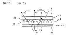
図1のA,Bには、光電素子100の実施例が示されている。ここで、図1のAには、駆動中の光電素子の様子が示されており、図1のBにはオフ状態での光電素子の様子が示されている。以下の説明においてもこのことが当てはまる。
1A and 1B show an embodiment of the
光電素子100は活性領域11を備えた半導体層列1を有している。半導体層列1は前述したように機能層または機能層列を有しており、例えば半導体チップとしてまたはOLEDとして構成される。特に半導体層列1の活性領域11は第1のスペクトルの電磁放射31を発光するのに適している。
The
第1のスペクトルの電磁放射31の光路には、波長変換物質22を含む波長変換層2が配置されている。本発明の有利な実施形態に挙げたように、波長変換物質22は例えば母型材料21内に埋め込まれる。波長変換物質22は第1のスペクトルの電磁放射31の部分スペクトルを少なくとも部分的に第2のスペクトルの電磁放射32へ変換するのに適している。波長変換物質22として、ここでは特に、第1のスペクトルの少なくとも1つのスペクトル成分ないし少なくとも1つの波長領域を吸収スペクトルとして含む材料が適している。吸収された電磁放射は有利には第1のスペクトルの電磁放射31とは異なる波長で再発光される。
In the optical path of the
図1の実施例では、第1のスペクトルの電磁放射31の光路および第2のスペクトルの電磁放射32の光路において、波長変換層2の上方にフィルタ層3が配置されている。フィルタ層3は、ここでは、光電素子100の駆動中およびオフ状態において、外部から当該の光電素子へ入射する放射33を図1のBに示されているように放射34として反射させることに適している。特に、外部から当該の光電素子へ入射する放射33は、フィルタ層3のうち波長変換層2の反対側の主表面4へ入射する。主表面4はここでは有利には光電素子100の光出射面である。特に、フィルタ層3は誘電体材料から成る第1の層および第2の層を周期的な順序で有しており、ここで、前述したように、第1の層は第1の屈折率を有し、第2の層は第1の屈折率と異なる第2の屈折率を有する。
In the embodiment of FIG. 1, the
特に、フィルタ層3は第1のスペクトルの電磁放射31の少なくとも一部312を反射するのに適している。第1のスペクトルの電磁放射31のうちフィルタ層3で反射された成分312は有利には波長変換層2へ戻され、そこで例えば波長変換物質22により第2のスペクトルの電磁放射32へ変換される。
In particular, the
フィルタ層3は波長変換層2の直上または少なくとも近傍に配置され、特に光電素子100のコンパクトな構造が達成される。またこれにより、光電素子の色印象は駆動中にもオフ状態においても均一となる。
The
光電素子の駆動中に観察者において喚起される色印象は、光出射面4から出射される電磁放射によって得られる色印象と同じである。この電磁放射は光電素子から出射された第1のスペクトルの電磁放射31の成分311と波長変換層2から放出された第2のスペクトルの電磁放射32とが重畳されたものである。特に、当該の色印象は、第1のスペクトルの電磁放射31の成分311と第2のスペクトルの電磁放射32との相対強度に基づいて定まる。
The color impression evoked by the observer during the driving of the photoelectric element is the same as the color impression obtained by the electromagnetic radiation emitted from the light exit surface 4. This electromagnetic radiation is a superposition of the
光電素子100のオフ状態では、図1のBに示されているように、半導体層列1の活性領域(活性層)11において第1のスペクトルの電磁放射31が形成されない。しかし、特に光出射面4が観察される場合、光電素子100の色印象が観察者に喚起されることがある。これは、外部から当該の光電素子へ入射する放射33の少なくとも一部が、当該の光電素子、特に波長変換層2、フィルタ層3および/または半導体層列1で反射されることによって起こる。図示の実施例に示されているように、外部から当該の光電素子へ入射する放射33の少なくとも一部は波長変換層2の吸収スペクトルに相応するスペクトルを有しており、波長変換層2において第2のスペクトルの電磁放射32へ変換され、外部へ放出される。このため、光電素子100のオフ状態において、望ましくない波長変換層2の色印象が観察者に喚起されうるのである。
In the OFF state of the
前述したように、フィルタ層3は外部から当該の光電素子100へ入射する放射33の一部を放射34として反射することに適している。特にそのスペクトルは、当該の放射34と波長変換層2によって変換された電磁放射32との重畳により、波長変換層2によって喚起される望ましくない色印象が回避されるように選定される。特にフィルタ層3は、外部から当該の光電素子100へ入射する放射33の一部が波長変換物質22の吸収スペクトルに含まれる1つまたは複数のスペクトルを有する放射34として反射されるように構成される。特に、当該のスペクトル成分は駆動中に半導体層列1の活性領域11によって形成される電磁放射31の第1のスペクトルにも含まれる。
As described above, the
フィルタ層3を波長変換層2の直上または少なくとも近傍に配置することにより、特に光電素子100のコンパクトな構造が得られ、駆動中にもオフ状態においても均一な色印象が達成される。
By disposing the
特に有利には、外部から当該の光電素子100へ入射する放射33のうちフィルタ層3で反射された成分34では、第1のスペクトルの電磁放射31のうちフィルタ層3で反射される成分312と同様に、フィルタ層3の主表面4とそれぞれの放射のフィルタ層3への入射方向とのなす角度9に基づいて、反射率が定められる。有利には、反射率は当該の角度9が小さくなるにつれて小さくなる。ここで、小さな角度9でフィルタ層3に入射してくる第1のスペクトルの電磁放射31ないし外部から当該の光電素子へ入射する放射33は、大きな角度、例えば90゜で入射してくる放射よりも早く送出される。
Particularly advantageously, the
純粋に実験的に得られたデータであるが、図示の実施例では、第1のスペクトルの電磁放射31は青色波長領域のスペクトル成分を有している。波長変換層2の波長変換物質22は、第1のスペクトルの電磁放射31の少なくとも一部、特に青色波長領域のスペクトル成分を、第2のスペクトルの電磁放射32、特に黄色波長領域のスペクトル成分へ変換するのに適している。これにより、光電素子100の光出射面4を介して、観察者に白色の色印象を与える電磁放射が送出される。オフ状態では、外部から当該の光電素子へ入射する放射33、例えば太陽光または昼間光に類似した室内照明の放射があるとき、波長変換層2が望ましくない黄色の色印象を形成する。このため、フィルタ層3は、外部から当該の光電素子100へ入射する放射33のうち青色波長領域のスペクトル成分を含む成分34を反射させ、波長変換層2の黄色の色印象とフィルタ層3の青色の色印象とが重畳されて観察者が光出射面4の白色の色印象を得るようにする。このとき、フィルタ層3は第1のスペクトルの電磁放射31の少なくとも一部、例えば50%を波長変換層2の方向へ反射させる。
Although purely experimentally obtained data, in the illustrated embodiment, the first spectral
ヒトの目の知覚の様態は波長すなわち測光法上の重みによって変化するので、光電素子100から送出される第1のスペクトルの電磁放射31の青色波長領域はフィルタ層3での反射により100%低減されてしまうことがある。ただし、波長変換層2で第2のスペクトルの電磁放射32へ変換された電磁放射の輝度は約3%しか低減されない。
Since the manner of perception of the human eye changes depending on the wavelength, that is, the weight in the photometric method, the blue wavelength region of the
本発明の光電素子100は例えばカメラを備えた移動電話のフラッシュライト部材として用いられるのに適している。さらに、こうした光電素子は照明装置にも適する。
The
以下に図1のA,Bの実施例の機能を利用した別の実施例を説明する。 In the following, another embodiment using the functions of the embodiments of FIGS. 1A and 1B will be described.
図2の実施例では、相互に対向する2つの主表面51,52を有する基板5を備えた光電素子200が示されている。当該の基板5は有利にはガラス基板である。これに代えてまたはこれに加えて、基板5は、プラスティックから成る1つまたは複数の層などの別の材料から成っていてもよい。
In the embodiment of FIG. 2, a
基板5のうち半導体層列1から遠い側の主表面51にフィルタ層3が被着されている。特にフィルタ層3は誘電体材料から成る複数の第1の層および複数の第2の層を周期的な順序で有する。第1の層および第2の層は基板5の主表面51に例えば蒸着により被着される。
The
基板5のうち半導体層列1に近い側の主表面52には波長変換層2が被着される。波長変換層2では例えば波長変換物質22が母型材料21内に埋め込まれている。これに代えて、波長変換物質22が母型材料21なしに主表面52に被着されて波長変換層2を形成していてもよい。
The
図3の実施例では、波長変換層2として波長変換物質22を有するシート21を備えた光学素子300が示されている。波長変換層2のうち半導体層列1から遠い側の主表面23にはフィルタ層3が前述した実施例と同様に被着されている。波長変換層2のうち半導体層列1に近い側の主表面24には透明な導電層6、例えば透明な導電性酸化物が被着されている。透明な導電層6は半導体層列1の電気コンタクトを容易にする。透明な導電層6は、半導体層列1の直上に波長変換物質22が被着される場合に設けられると特に有利である。
In the embodiment of FIG. 3, an
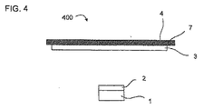
図4には、付加的な光学素子7を備えた光電素子400の実施例が示されている。例えば光学素子7はマイクロプリズム構造体などの光学系を内部に含むカバーである。ここで、光学素子7は例えば光電素子400のケーシングの一部であってもよい。その場合、フィルタ層3は光学素子7の上に被着され、フィルタ層3は波長変換層2に間接的に接することになる。
FIG. 4 shows an embodiment of a
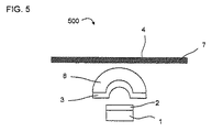
図5の実施例では、例えばカバーである光学素子7のほか、さらに別の第2の光学素子8を有する光電素子500が示されている。第2の光学素子8は例えばレンズまたはその他の屈折性ないし回折性の光学素子である。この場合、フィルタ層3は第2の光学素子8の面、特に半導体層列1に近い側の表面に配置されるかまたは被着される。
In the embodiment of FIG. 5, for example, a
図示の実施例では、特に、波長変換層2および/またはフィルタ層3は半導体層列1の複数の表面、例えば側面などにも配置することができる。
In the illustrated embodiment, in particular, the
本発明は前述した実施例に限定されない。本発明の新規な特徴は単独でも任意に組み合わせても本発明の対象となりうる。このことは、それぞれの特徴が実施例ないし特許請求の範囲に明示的に示されていない場合にも当てはまる。 The present invention is not limited to the embodiments described above. The novel features of the present invention can be the subject of the present invention alone or in any combination. This is true even if the respective features are not explicitly indicated in the examples or claims.
Claims (25)
該第1のスペクトルの電磁放射の光路で見て前記半導体層列の後方に配置され、該第1のスペクトルの電磁放射の少なくとも一部を第2のスペクトルの電磁放射(32)へ変換する波長変換層(2)と、
外部から当該の光電素子へ入射する放射(33)のうち少なくとも一部(34)を反射するフィルタ層(3)と
を有する
ことを特徴とする光電素子。 A semiconductor layer sequence (1) with an active region (11) that emits electromagnetic radiation (31) of the first spectrum when driven;
A wavelength disposed behind the semiconductor layer sequence as viewed in the optical path of the electromagnetic radiation of the first spectrum and converting at least a part of the electromagnetic radiation of the first spectrum into electromagnetic radiation (32) of the second spectrum A conversion layer (2);
And a filter layer (3) that reflects at least a part (34) of radiation (33) incident on the photoelectric element from the outside.
Applications Claiming Priority (2)
| Application Number | Priority Date | Filing Date | Title |
|---|---|---|---|
| DE102006046199A DE102006046199A1 (en) | 2006-09-29 | 2006-09-29 | Optoelectronic component, has semiconductor layer sequence with active area, which emits electromagnetic radiations with spectrum in operation |
| PCT/DE2007/001611 WO2008040283A1 (en) | 2006-09-29 | 2007-09-07 | Optoelectronic component |
Publications (2)
| Publication Number | Publication Date |
|---|---|
| JP2010505247A true JP2010505247A (en) | 2010-02-18 |
| JP2010505247A5 JP2010505247A5 (en) | 2011-07-07 |
Family
ID=38982837
Family Applications (1)
| Application Number | Title | Priority Date | Filing Date |
|---|---|---|---|
| JP2009529517A Pending JP2010505247A (en) | 2006-09-29 | 2007-09-07 | Photoelectric element |
Country Status (8)
| Country | Link |
|---|---|
| US (1) | US8093610B2 (en) |
| EP (1) | EP2054948A1 (en) |
| JP (1) | JP2010505247A (en) |
| KR (1) | KR101313963B1 (en) |
| CN (1) | CN101517761B (en) |
| DE (1) | DE102006046199A1 (en) |
| TW (1) | TW200830591A (en) |
| WO (1) | WO2008040283A1 (en) |
Cited By (1)
| Publication number | Priority date | Publication date | Assignee | Title |
|---|---|---|---|---|
| JP2015517717A (en) * | 2012-05-09 | 2015-06-22 | コーニンクレッカ フィリップス エヌ ヴェ | Light emitting device |
Families Citing this family (26)
| Publication number | Priority date | Publication date | Assignee | Title |
|---|---|---|---|---|
| DE102007046339A1 (en) | 2007-09-27 | 2009-04-02 | Osram Opto Semiconductors Gmbh | Light source with variable emission characteristics |
| DE102008020817A1 (en) * | 2008-04-25 | 2009-10-29 | Osram Opto Semiconductors Gmbh | light unit |
| US20100129641A1 (en) * | 2008-11-25 | 2010-05-27 | Lopez Leonardo C | Polymer carbon composites |
| US8440297B2 (en) * | 2008-11-25 | 2013-05-14 | Dow Global Technologies Llc | Polymer organoclay composites |
| US20100127434A1 (en) * | 2008-11-25 | 2010-05-27 | Rene Broos | Extruding organic polymers |
| US8547010B2 (en) * | 2009-03-19 | 2013-10-01 | Koninklijke Philips N.V. | Color adjusting arrangement |
| WO2010132539A2 (en) * | 2009-05-14 | 2010-11-18 | Photonic Glass Corporation | Methods and apparatus for wavelength conversion in solar cells and solar cell covers |
| US20110012147A1 (en) * | 2009-07-15 | 2011-01-20 | Koninklijke Philips Electronics N.V. | Wavelength-converted semiconductor light emitting device including a filter and a scattering structure |
| DE102009054067A1 (en) * | 2009-11-20 | 2011-05-26 | Osram Opto Semiconductors Gmbh | Light emitting device |
| WO2011127622A1 (en) * | 2010-04-12 | 2011-10-20 | 绎立锐光科技开发(深圳)有限公司 | Method for improving emitted light color based on light wavelength conversion |
| US8154052B2 (en) * | 2010-05-06 | 2012-04-10 | Koninklijke Philips Electronics N.V. | Light emitting device grown on wavelength converting substrate |
| JP5257420B2 (en) * | 2010-08-04 | 2013-08-07 | ウシオ電機株式会社 | Light source device |
| CN101964387A (en) * | 2010-08-25 | 2011-02-02 | 柳翠 | Led chip structure |
| DE102011050450A1 (en) | 2011-05-18 | 2012-11-22 | Osram Opto Semiconductors Gmbh | Optoelectronic semiconductor chip, optoelectronic semiconductor component and method for producing an optoelectronic semiconductor component |
| CN103636023B (en) * | 2011-06-30 | 2016-09-14 | 欧司朗Oled股份有限公司 | Encapsulating structure for opto-electronic device and the method for packaging optoelectronic device |
| DE102012111123A1 (en) * | 2012-09-26 | 2014-03-27 | Osram Opto Semiconductors Gmbh | Light-emitting semiconductor device |
| US9797573B2 (en) | 2013-08-09 | 2017-10-24 | Performance Indicator, Llc | Luminous systems |
| US9206958B2 (en) * | 2013-09-16 | 2015-12-08 | Osram Sylvania Inc. | Thin film wavelength converters and methods for making the same |
| DE102013112740B4 (en) * | 2013-11-19 | 2021-03-18 | OSRAM Opto Semiconductors Gesellschaft mit beschränkter Haftung | Radiation-emitting semiconductor component |
| CN104617197B (en) * | 2015-01-08 | 2017-08-01 | 青岛海信电器股份有限公司 | A kind of display module LED and display module |
| WO2017007933A1 (en) | 2015-07-08 | 2017-01-12 | Performance Indicator, Llc | Led panel lighting system |
| US10886437B2 (en) * | 2016-11-03 | 2021-01-05 | Lumileds Llc | Devices and structures bonded by inorganic coating |
| US10243124B2 (en) * | 2016-12-26 | 2019-03-26 | Nichia Corporation | Light emitting device |
| DE102017101729A1 (en) * | 2017-01-30 | 2018-08-02 | Osram Opto Semiconductors Gmbh | Radiation-emitting device |
| EP3457444A1 (en) * | 2017-09-19 | 2019-03-20 | ams AG | Phosphor-converted light-emitting device |
| DE102017130136A1 (en) * | 2017-12-15 | 2019-06-19 | Osram Opto Semiconductors Gmbh | Optoelectronic semiconductor component |
Citations (5)
| Publication number | Priority date | Publication date | Assignee | Title |
|---|---|---|---|---|
| JPH11145519A (en) * | 1997-09-02 | 1999-05-28 | Toshiba Corp | Semiconductor light-emitting element, semiconductor light-emitting device, and image-display device |
| JP2001501380A (en) * | 1997-05-27 | 2001-01-30 | コーニンクレッカ フィリップス エレクトロニクス エヌ ヴィ | Ultraviolet / blue LED-phosphor device that efficiently converts ultraviolet / blue light into visible light |
| JP2004193581A (en) * | 2002-11-25 | 2004-07-08 | Matsushita Electric Ind Co Ltd | Led illumination light source |
| JP2005294288A (en) * | 2004-03-31 | 2005-10-20 | Mitsubishi Cable Ind Ltd | Phosphor light emitting device and endoscope equipment therewith as lighting source |
| JP2006261540A (en) * | 2005-03-18 | 2006-09-28 | Stanley Electric Co Ltd | Light emitting device |
Family Cites Families (19)
| Publication number | Priority date | Publication date | Assignee | Title |
|---|---|---|---|---|
| DE19638667C2 (en) * | 1996-09-20 | 2001-05-17 | Osram Opto Semiconductors Gmbh | Mixed-color light-emitting semiconductor component with luminescence conversion element |
| US5813752A (en) * | 1997-05-27 | 1998-09-29 | Philips Electronics North America Corporation | UV/blue LED-phosphor device with short wave pass, long wave pass band pass and peroit filters |
| US6252254B1 (en) | 1998-02-06 | 2001-06-26 | General Electric Company | Light emitting device with phosphor composition |
| JP2001111109A (en) * | 1999-10-07 | 2001-04-20 | Sharp Corp | Gallium nitride compound semiconductor light emitting device |
| US6616862B2 (en) * | 2001-05-21 | 2003-09-09 | General Electric Company | Yellow light-emitting halophosphate phosphors and light sources incorporating the same |
| DE10142009B4 (en) * | 2001-08-28 | 2010-04-22 | Osram Opto Semiconductors Gmbh | LED light source with a conversion agent and with a UV absorbing layer |
| DE10147040A1 (en) * | 2001-09-25 | 2003-04-24 | Patent Treuhand Ges Fuer Elektrische Gluehlampen Mbh | Lighting unit with at least one LED as a light source |
| JP4263453B2 (en) * | 2002-09-25 | 2009-05-13 | パナソニック株式会社 | Inorganic oxide and light emitting device using the same |
| US6744077B2 (en) | 2002-09-27 | 2004-06-01 | Lumileds Lighting U.S., Llc | Selective filtering of wavelength-converted semiconductor light emitting devices |
| JP4143732B2 (en) * | 2002-10-16 | 2008-09-03 | スタンレー電気株式会社 | In-vehicle wavelength converter |
| US7118438B2 (en) * | 2003-01-27 | 2006-10-10 | 3M Innovative Properties Company | Methods of making phosphor based light sources having an interference reflector |
| US7256057B2 (en) * | 2004-09-11 | 2007-08-14 | 3M Innovative Properties Company | Methods for producing phosphor based light sources |
| DE102004047727B4 (en) * | 2004-09-30 | 2018-01-18 | Osram Opto Semiconductors Gmbh | Luminescence diode chip with a converter layer and method for producing a luminescence diode chip with a converter layer |
| JP2006135002A (en) * | 2004-11-04 | 2006-05-25 | Koito Mfg Co Ltd | Light-emitting device and lighting fixture for car |
| CN100438095C (en) | 2005-01-14 | 2008-11-26 | 财团法人工业技术研究院 | Light emitting diode with quasi-omnibearing reflector |
| US20060171152A1 (en) * | 2005-01-20 | 2006-08-03 | Toyoda Gosei Co., Ltd. | Light emitting device and method of making the same |
| JP4492378B2 (en) | 2005-02-03 | 2010-06-30 | 豊田合成株式会社 | Light emitting device and manufacturing method thereof |
| DE102005019375A1 (en) * | 2005-02-28 | 2006-09-07 | Osram Opto Semiconductors Gmbh | LED array |
| US7341878B2 (en) * | 2005-03-14 | 2008-03-11 | Philips Lumileds Lighting Company, Llc | Wavelength-converted semiconductor light emitting device |
-
2006
- 2006-09-29 DE DE102006046199A patent/DE102006046199A1/en not_active Withdrawn
-
2007
- 2007-09-07 US US12/443,305 patent/US8093610B2/en not_active Expired - Fee Related
- 2007-09-07 JP JP2009529517A patent/JP2010505247A/en active Pending
- 2007-09-07 WO PCT/DE2007/001611 patent/WO2008040283A1/en active Application Filing
- 2007-09-07 CN CN2007800360698A patent/CN101517761B/en not_active Expired - Fee Related
- 2007-09-07 EP EP07817484A patent/EP2054948A1/en not_active Withdrawn
- 2007-09-07 KR KR1020097008770A patent/KR101313963B1/en active IP Right Grant
- 2007-09-27 TW TW096135848A patent/TW200830591A/en unknown
Patent Citations (5)
| Publication number | Priority date | Publication date | Assignee | Title |
|---|---|---|---|---|
| JP2001501380A (en) * | 1997-05-27 | 2001-01-30 | コーニンクレッカ フィリップス エレクトロニクス エヌ ヴィ | Ultraviolet / blue LED-phosphor device that efficiently converts ultraviolet / blue light into visible light |
| JPH11145519A (en) * | 1997-09-02 | 1999-05-28 | Toshiba Corp | Semiconductor light-emitting element, semiconductor light-emitting device, and image-display device |
| JP2004193581A (en) * | 2002-11-25 | 2004-07-08 | Matsushita Electric Ind Co Ltd | Led illumination light source |
| JP2005294288A (en) * | 2004-03-31 | 2005-10-20 | Mitsubishi Cable Ind Ltd | Phosphor light emitting device and endoscope equipment therewith as lighting source |
| JP2006261540A (en) * | 2005-03-18 | 2006-09-28 | Stanley Electric Co Ltd | Light emitting device |
Cited By (1)
| Publication number | Priority date | Publication date | Assignee | Title |
|---|---|---|---|---|
| JP2015517717A (en) * | 2012-05-09 | 2015-06-22 | コーニンクレッカ フィリップス エヌ ヴェ | Light emitting device |
Also Published As
| Publication number | Publication date |
|---|---|
| EP2054948A1 (en) | 2009-05-06 |
| KR101313963B1 (en) | 2013-10-01 |
| TW200830591A (en) | 2008-07-16 |
| CN101517761A (en) | 2009-08-26 |
| KR20090080053A (en) | 2009-07-23 |
| CN101517761B (en) | 2012-12-19 |
| US8093610B2 (en) | 2012-01-10 |
| US20100012959A1 (en) | 2010-01-21 |
| WO2008040283A1 (en) | 2008-04-10 |
| DE102006046199A1 (en) | 2008-04-03 |
Similar Documents
| Publication | Publication Date | Title |
|---|---|---|
| JP2010505247A (en) | Photoelectric element | |
| US9373759B2 (en) | Light-emitting semiconductor component | |
| US8941566B2 (en) | Array of luminescent elements | |
| US8314547B2 (en) | Opto-electronic component | |
| US20050110032A1 (en) | Light-Emitting Diode and Semiconductor Light-Emitting Device | |
| KR101559601B1 (en) | Radiation-emitting device | |
| US8987708B2 (en) | Optoelectronic component | |
| JP2009076911A (en) | Optoelectronic device and manufacturing method of optoelectronic device | |
| KR20100059854A (en) | Radiation-emitting semiconductor body | |
| KR102471271B1 (en) | Optical device and light source module having the same | |
| TW201031246A (en) | OLED device with adjustable color appearance | |
| KR101157705B1 (en) | Light Emitting Device Having Fluorescent Substance Unit Isolated From Mold Unit | |
| WO2014032702A1 (en) | Light-emitting device and method for manufacturing a light- emitting device | |
| KR20190117308A (en) | Light emitting device package | |
| KR102242660B1 (en) | Light Emitting Diode Device And Back Light Unit Including The Same And Method Of Manufacturing The Same | |
| US11316077B2 (en) | Radiation-emitting device | |
| US20130113366A1 (en) | Color control of solid state light sources | |
| KR20240007644A (en) | Light emitting module and display device having same | |
| KR20220048114A (en) | Display appartus | |
| CN117690916A (en) | Light-emitting panel and electronic equipment | |
| JP2004304048A (en) | Epitaxial wafer for light emitting diode |
Legal Events
| Date | Code | Title | Description |
|---|---|---|---|
| A621 | Written request for application examination |
Free format text: JAPANESE INTERMEDIATE CODE: A621 Effective date: 20100629 |
|
| RD04 | Notification of resignation of power of attorney |
Free format text: JAPANESE INTERMEDIATE CODE: A7424 Effective date: 20101228 |
|
| A521 | Written amendment |
Free format text: JAPANESE INTERMEDIATE CODE: A523 Effective date: 20110519 |
|
| A131 | Notification of reasons for refusal |
Free format text: JAPANESE INTERMEDIATE CODE: A131 Effective date: 20130125 |
|
| A521 | Written amendment |
Free format text: JAPANESE INTERMEDIATE CODE: A523 Effective date: 20130424 |
|
| A131 | Notification of reasons for refusal |
Free format text: JAPANESE INTERMEDIATE CODE: A131 Effective date: 20130902 |
|
| A601 | Written request for extension of time |
Free format text: JAPANESE INTERMEDIATE CODE: A601 Effective date: 20131107 |
|
| A602 | Written permission of extension of time |
Free format text: JAPANESE INTERMEDIATE CODE: A602 Effective date: 20131114 |
|
| A521 | Written amendment |
Free format text: JAPANESE INTERMEDIATE CODE: A523 Effective date: 20140214 |
|
| A02 | Decision of refusal |
Free format text: JAPANESE INTERMEDIATE CODE: A02 Effective date: 20140623 |