JP2010219072A - Connection terminal for circuit board - Google Patents
Connection terminal for circuit board Download PDFInfo
- Publication number
- JP2010219072A JP2010219072A JP2010155846A JP2010155846A JP2010219072A JP 2010219072 A JP2010219072 A JP 2010219072A JP 2010155846 A JP2010155846 A JP 2010155846A JP 2010155846 A JP2010155846 A JP 2010155846A JP 2010219072 A JP2010219072 A JP 2010219072A
- Authority
- JP
- Japan
- Prior art keywords
- circuit board
- terminal
- circuit
- pin
- foil
- Prior art date
- Legal status (The legal status is an assumption and is not a legal conclusion. Google has not performed a legal analysis and makes no representation as to the accuracy of the status listed.)
- Granted
Links
- 238000003780 insertion Methods 0.000 claims abstract description 66
- 230000037431 insertion Effects 0.000 claims abstract description 66
- 239000011888 foil Substances 0.000 claims abstract description 43
- 229920005989 resin Polymers 0.000 claims abstract description 36
- 239000011347 resin Substances 0.000 claims abstract description 36
- 238000003466 welding Methods 0.000 claims description 10
- 239000004020 conductor Substances 0.000 claims description 3
- RYGMFSIKBFXOCR-UHFFFAOYSA-N Copper Chemical compound [Cu] RYGMFSIKBFXOCR-UHFFFAOYSA-N 0.000 description 18
- 239000011889 copper foil Substances 0.000 description 17
- 239000002184 metal Substances 0.000 description 11
- 229910052751 metal Inorganic materials 0.000 description 11
- 238000000034 method Methods 0.000 description 9
- 239000000463 material Substances 0.000 description 5
- 229920003002 synthetic resin Polymers 0.000 description 5
- 239000000057 synthetic resin Substances 0.000 description 5
- 238000004080 punching Methods 0.000 description 4
- 238000004519 manufacturing process Methods 0.000 description 3
- 229910001369 Brass Inorganic materials 0.000 description 2
- 239000010951 brass Substances 0.000 description 2
- 238000003384 imaging method Methods 0.000 description 2
- 238000001746 injection moulding Methods 0.000 description 2
- 210000000078 claw Anatomy 0.000 description 1
- 229910052802 copper Inorganic materials 0.000 description 1
- 239000010949 copper Substances 0.000 description 1
- 238000005520 cutting process Methods 0.000 description 1
- 238000010586 diagram Methods 0.000 description 1
- 238000005242 forging Methods 0.000 description 1
- 238000007731 hot pressing Methods 0.000 description 1
- 238000010030 laminating Methods 0.000 description 1
- 238000002844 melting Methods 0.000 description 1
- 230000008018 melting Effects 0.000 description 1
- 238000000465 moulding Methods 0.000 description 1
- 239000003973 paint Substances 0.000 description 1
- 239000000758 substrate Substances 0.000 description 1
Images


Abstract
Description
本発明は、各種電気回路において使用される受型の回路基板用接続端子に関するものである。 The present invention relates to a receiving terminal for a circuit board used in various electric circuits.
例えば、特許文献1にはプリント基板の接続構造が開示されている。 For example, Patent Document 1 discloses a printed circuit board connection structure.
しかし、特許文献1の接続構造は部品点数が多いという問題がある。 However, the connection structure of Patent Document 1 has a problem that the number of parts is large.
本発明の目的は、ピン状端子の挿入端との接続を容易にすると共に確実な固定を保証し、小型軽量で安価な回路基板用接続端子を提供することにある。 An object of the present invention is to provide a circuit board connection terminal that facilitates connection with an insertion end of a pin-shaped terminal and ensures secure fixation, and is small, light, and inexpensive.
上記目的を達成するための本発明に係る回路基板用接続端子は、箔回路のピン孔に樹脂プレートのアンカピンを挿通することにより前記箔回路を前記樹脂プレートの表面に位置決め固定して成る回路基板に設けた端子挿入孔に挿入して使用し、ピン状端子の挿入端を受け入れる受型の接続端子であって、上部周囲にフランジ部を設け該フランジ部により前記端子挿入孔に対し下方向に固定し、下端を前記端子挿入孔内に配置し、前記ピン状端子の挿入端を受け入れる短円筒状の筒状接続部と、前記フランジ部の一部から側方に延出し前記箔回路の一部に重ね、表側に接触した電極と前記回路基板の裏側に設けた溶着用孔部から挿入して前記箔回路に接触した電極とを用いて前記箔回路に溶着した導体接続部とを備えたことを特徴とする。 In order to achieve the above object, a circuit board connection terminal according to the present invention comprises a circuit board formed by positioning and fixing the foil circuit on the surface of the resin plate by inserting an anchor pin of the resin plate into a pin hole of the foil circuit. It is a receiving type connection terminal that is used by inserting into the terminal insertion hole provided in the terminal, and accepts the insertion end of the pin-shaped terminal. A short cylindrical connection part that receives the insertion end of the pin-like terminal, extends from a part of the flange part to the side, and is one side of the foil circuit. And a conductor connecting portion welded to the foil circuit using an electrode in contact with the front side and an electrode in contact with the foil circuit inserted from a welding hole provided on the back side of the circuit board. It is characterized by that.
本発明に係る回路基板用接続端子によれば、ピン状端子の挿入端を受け入れて信頼性のある接続を可能とする。 According to the circuit board connection terminal of the present invention, the insertion end of the pin-shaped terminal is received to enable reliable connection.
本発明を図示の実施例に基づいて詳細に説明する。
図1は本発明に係る回路基板用接続端子である受端子を使用するジョイントボックスの分解斜視図であり、上ケース11、回路ユニット12、下ケース13を相互に組み付けることにより、ボックス形状のジョイントボックスが得られる。つまり、上ケース11、下ケース13間に回路ユニット12が収納され、ケース11、13同士が接合されると、回路ユニット12を収容した状態で上ケース11、下ケース13に設けられたロック部14a、14bによりロックされる。
The present invention will be described in detail based on the embodiments shown in the drawings.
FIG. 1 is an exploded perspective view of a joint box using a receiving terminal which is a circuit board connection terminal according to the present invention. By assembling an
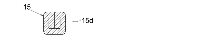
回路ユニット12の上面には、図示を省略した回路パターンが形成されていると共に、複数個の挿入端子15を取り付けた合成樹脂製のブロック体16が配置されている。ブロック体16は上ケース11に区画された枠部17に嵌合され、ブロック体16上に突出した挿入端子15の平刃端15a、受端15b、ピン端15cなどの接続部が上ケース11の枠部17内に位置し、これらの接続部にヒューズ素子、スイッチ素子或いは他の接続端子を収容したコネクタが装着可能とされている。
A circuit pattern (not shown) is formed on the upper surface of the
また、下ケース13においても枠部18が形成され、図示は省略しているが、回路ユニット12の下面に取り付けられたブロック体16から挿入端子15の接続端が下向きに突出され、下ケース13の下面に同様の素子、コネクタなどが装着可能とされている。
The
回路ユニット12は例えば5枚の回路基板19が積層され、図2、図3に示すように、各回路基板19は例えば射出成型により成型された合成樹脂製の最大厚み1.5mm程度の樹脂プレート20上に、例えば厚さ120μmの銅箔から成り、積層された回路基板19ごとに異なるように区画されたパターンの箔回路21が載置されている。
For example, five
樹脂プレート20には、図4に示すように複数のアンカピン20aが上方に向けて突出され、箔回路21に設けられたピン孔21aに挿通され、アンカピン20aの上部を熱により押し潰すことにより、箔回路21は樹脂プレート20に位置決め固定されている。
As shown in FIG. 4, a plurality of
なお、電流容量によっては一部の箔回路21は、図5に示すように金属箔を2層又はそれ以上の複数層とされ、高さの高いアンカピン20a’により固定され、樹脂プレート20に穿孔された溶着用孔部20bから溶着電極を挿し込んで、金属箔同士は溶着されている。
Depending on the current capacity, a part of the
樹脂プレート20の複数個所には、図2、図3に示すように積層した樹脂プレート20に共通の円形の端子挿通孔20cが形成され、所定の層の回路基板19の端子挿通孔20cには受端子22が取り付けられている。なお、受端子22は必要な電流容量によって数種類の大きさがあり、それに伴って端子挿通孔20cの径も数種類設けられている。
As shown in FIGS. 2 and 3, circular
受端子22は例えば肉厚0.2mmの黄銅板から成り、フォーミングプレスにより形成され、図6に示すように短円筒状に形成した筒状接続部22aの上部にフランジ部22bが形成され、更にフランジ部22bの一部にタブ22cが付設されている。なお、筒状接続部22aとフランジ部22bとの境界部は、後述する挿入端子を受け入れるためのテーパ状の案内部22dとされている。
The
図7は5枚の回路基板19を積層し、受端子22を固定した状態の回路ユニット12の要部断面図であり、回路基板19の端子挿通孔20cの中間部の径を受端子22の筒状接続部22aの外径とほぼ同じとし、端子挿通孔20cの上部の周囲は上方に持ち上げられた円環部20dとされ、この円環部20d内に受端子22のフランジ部22bを載置する段部20eが形成され、端子挿通孔20cの下部は筒状接続部22aの下端を拡開するために内径が大きくされている。
FIG. 7 is a cross-sectional view of the main part of the
受端子22の筒状接続部22aは端子挿通孔20c内に配置され、筒状接続部22aの下端は端子挿通孔20cの下部にテーパ状にかしめ止めされている。この筒状接続部22aの下端の拡開は、受端子22の回路基板19への固定を主目的としているが、下面方向から挿入端子15を挿し込む場合におけるテーパ状の案内部22eともなっている。また、タブ22cは回路基板19の箔回路21上に溶着により接続されており、この溶着のためにタブ22cの下方の樹脂プレート20には、電極挿通のための溶着用孔部20fが形成されている。
The
回路基板19の受端子22を取り付けない端子挿通孔20cにおいては、その上部周囲に円環部20gが形成され、端子挿通孔20cに挿入される挿入端子15が箔回路21と接触しないようにされている。なお、回路ユニット12の最上位の回路基板19に設けた円環部20gは、ブロック体16を安定して載置するために、受端子22を取り付ける孔部20cに設けた円環部20dと同じ高さとされている。
In the
また図2、図3に示すように、樹脂プレート20の下面側には必要に応じて電線用溝部20hが形成され、この電線用溝部20h内に絶縁塗料が塗布された例えば角型電線23が装着され、角型電線23の両端部は電線用溝部20hの両端に設けられた電線用孔部20iを介して立ち上げられて箔回路21の下面と溶着し、回路設計上樹脂プレート20の表面においては、短絡できない箔回路21のパターン同士をジャンパ線として短絡するようにされている。なお、この角型電線23は電流容量に応じて各種断面積のものが使用されている。
As shown in FIGS. 2 and 3, a
上述の回路基板19のアンカピン20aの熱溶融した上端部、円環部20d、受端子22は、上層の樹脂プレート20の下面に形成した凹部に嵌まり込み、積層した回路基板19同士が密着すると共に、水平方向にずれないようにされている。例えば、図3に示す凹部20jは、下層の回路基板19に取り付けた受端子22が嵌まり込む部分である。また、回路基板19の四隅に設けた透孔24は回路基板19を積層する場合の位置合わせ孔である。
The heat-melted upper end portion, the
また、回路基板19に設けられた図2、図3に示す角孔25は、挿入端子15、受端子22では電流容量が足りない場合に、図1に示す大電流用の接続端子26を取り付けるためのものであり、回路ユニット12の最上位の回路基板19のみに設けられている。
2 and 3 provided in the
回路基板19は全ての箔回路21を上に向けて積層するとは限らず、図7においては上層の3層の回路基板19は箔回路21を上に向けて積層し、下層の2層の回路基板19は箔回路21を下に向けて積層されている。この場合においても、3層目と4層目の下面同士を重ねた回路基板19では、図示を省略しているが、ずれないように部分的に嵌合し得るようにされている。
The
図8は受端子22に挿入するための挿入端子15の斜視図を示し、挿入端子15の下部は受端子22の筒状接続部22aに挿入するための図9に示すような断面略四角形のピン状挿入端15dとされ、中間部15eを介して上部は上ケース11上に突出して他の接続端子と接続するための平刃端15aとされている。なお、この平刃端15aは、図1に示す受端15b或いはピン端15cとすることもできる。
FIG. 8 is a perspective view of the
この挿入端子15は例えば厚み0.3mmの黄銅から成る金属板31を断裁、成形して製造され、挿入端15dは図10の工程に示すように、金属板31を積層しながら鍛造することにより強度を持たせている。つまり、金属板31を(a)に示すように金属板31の長手方向に沿った両側部32、33のように基部34に対して上方に立ち上げると共に、(b)に示すように両側部32、33を内側に曲げ、更に(c)に示すように基部34上に折り畳む。
The
続いて、(d)に示すように折り畳んだ両側部32、33を基部34と共に立ち上げて、両側部32、33同士を密着させ、四方から機械的に圧縮して図9に示すような断面形状とする。なお図10(d)に示すように、基部34を下方に稍々膨らんだ形状のままとしてもよい。
Subsequently, as shown in FIG. 9 (d), the folded
この挿入端15dによれば、板厚の薄い金属板31を折り曲げ、空洞部がなく上下方向に幅のある断面略四角形の棒状に形成しているので、金属板31の板厚が薄い場合でも、金属板31の厚みと比較して一辺の厚みが十分に大きい挿入端15dを得ることができ、挿入端15dが弯曲したり或いは折損することが少ない。また、上部の平刃端15aも金属板31を二重に折り畳んで厚みを持たせている。
According to the
更に、受端子22への挿入時にクリック感を得るためと、接続を良好とするために、挿入端15dに複数の段部を形成してもよい。また、これらの挿入端15dは受端子22の大きさに合わせて数種類用意されている。
Further, a plurality of step portions may be formed on the
合成樹脂材によるブロック体16に設けられた挿通孔には、幾つかの挿入端子15の中間部15eが挿し込まれて固定され、図1に示すように、挿入端15dはまとめて回路基板19に挿入されている。なお、挿入端子15の中間部15eには、挿通孔に固定するための図示しない爪部が設けられている。
図11に示すように、ブロック体16の底部には単数又は複数の下方を向くアンカピン16aが一体に形成されており、箔回路21に設けられたピン孔21b、各樹脂プレート20に共通に設けられたピン孔20kに挿通され、最下層の回路基板19から下方に突出したアンカピン16aの下端を溶融して押し潰すことにより、ブロック体16を回路ユニット12に固定すると共に、回路基板19の積層体同士を分離不能に固定している。
As shown in FIG. 11, one or a plurality of downwardly facing anchor pins 16 a are integrally formed at the bottom of the
図12は回路基板19の製造工程の説明図である。箔回路21の母材である銅箔41はローラ42にコイル状に巻回されており、予め銅箔41に形成されたパイロット孔を基に、送りローラ43により間欠的に繰り出される。銅箔41は孔あけプレス工程に搬送され、孔あけプレス44により複数の所定位置にピン孔21a、21bが穿孔され、樹脂プレート20との積層工程に移送される。なお、銅箔41に設けるピン孔21aは箔回路21を樹脂プレート20に固定するものであるので、樹脂プレート20上に残り、箔回路21となるべき部分に設けられる。
FIG. 12 is an explanatory diagram of the manufacturing process of the
一方、樹脂プレート20はストッカ45に積層されており、銅箔41の搬送に同期して1枚ずつ取り出される。樹脂プレート20は合成樹脂膜を射出成形或いは合成樹脂基材をホットプレスすることにより製造され、アンカピン20a、孔部20b、20f、端子挿通孔20c、ピン孔20k、円環部20d、20g、電線用溝部20h、透孔24等が既に形成されている。
On the other hand, the
1枚の樹脂プレート20が積層台46上に載置されると、積層台46は上昇して銅箔41に向けて押し上げられる。樹脂プレート20のアンカピン20aが銅箔41に穿孔されたピン孔21aに入り込むように、撮像カメラ47による画像処理によって積層台46は三次元的に位置制御される。
When one
なお、特に電流容量を要する箔回路21には、前述したように銅箔41を二重に重ねて電気抵抗を少なくするので、上述の工程を2回繰り返し、図示しない工程により、重ねられた銅箔41同士を図5に示したように樹脂プレート20に設けた溶着用孔部20bを用いて溶着する。
In particular, in the
アンカピン20aをピン孔21aに挿入して銅箔41を樹脂プレート20上に重ねた後に、積層台46の上方に位置する熱プレス48を降下し、アンカピン20aの頂部を熱により押し潰し、銅箔41が樹脂プレート20から剥離しないようにする。なお、位置合わせに伴って、ブロック体16のアンカピン16aを挿通する銅箔41のピン孔21bは、樹脂プレート20のピン孔20kと一致している。
After the
続いて、樹脂プレート20と一体となった銅箔41を打ち抜きプレス49に搬送し、画像処理を行いながら銅箔41から箔回路21を打ち抜く。上側の打ち抜きプレス49はビク刃49aを有し、樹脂プレート20を傷付けることなく銅箔41から箔回路21を打ち抜くものであり、ビク刃49aによって箔回路21の回路パターンが打ち抜かれることになる。
Subsequently, the
更に、樹脂プレート20と共に銅箔41を搬送し、箔回路21で使用されない残材の銅箔41は、樹脂プレート20から剥離された後に残材処理刃50により細断され、残材ボックス51内に投棄される。一方、箔回路21を表面に一体に固定した樹脂プレート20は、回路基板19として所定方向に搬出され、ストッカ52内に積層される。
Further, the
図13〜図15は回路基板19に受端子22を固定する工程の説明図であり、パーツフィーダにより整列して供給される受端子22を図13に示すように、ロボットハンド61により撮像カメラ62により画像処理を行いながら保持して、回路基板19の必要個所に運搬する。ロボットハンド61には筒部63に対して吊り上げピン64が上下動自在に設けられており、この吊り上げピン64を受端子22の筒状接続部22aに挿入し、摩擦抵抗により受端子22を持ち上げ、受端子22のタブ22cが箔回路21上に載置されるように、画像処理により位置調整しながら受端子22を樹脂プレート20の端子挿通孔20cに挿入する。
FIG. 13 to FIG. 15 are explanatory views of a process of fixing the receiving
筒部63により受端子22を樹脂プレート20の段部20e上に押し付けたまま、吊り上げピン64を図14に示すように上方に持ち上げ、続いて下方から先端を円錐状としたプレスピン65を持ち上げて、筒状接続部22aの下部を押し拡げ、受端子22を端子挿通孔20cの下部にかしめ止めする。
While the receiving
その後に、図15に示すようにタブ22cを箔回路21に電極66、67を用いて溶着する。電極66、67の先端はそれぞれ直径1mm前後の細径丸型とされ、上方の電極66はタブ22cに接触し、下方の電極67は箔回路21の下面に溶着用孔部20fを介して接触する。なお、この溶着はロボットハンドにより順次に行うこともできるが、多数本の電極を用いて一括して溶着することもできる。
Thereafter, as shown in FIG. 15, the
このようにして製作され、それぞれ回路パターンが異なる複数枚の回路基板19を積層し、図11に示すようにブロック体16を回路基板19の積層体上に載置し、ブロック体16に固定された挿入端子15の挿入端15dを、回路基板19の端子挿通孔20cに挿入すると、挿入端15dは少なくとも何れかの回路基板19に取り付けられた受端子22の筒状接続部22aに挿入される。
A plurality of
このとき、挿入端15dは断面略四角状とされているので、受端子22の筒状接続部22aに挿入された場合に角部が良好に接触し、挿入端子15は何れかの回路基板19の箔回路21と良好な電気的な接続がなされることになる。また必要に応じて、回路ユニット12の下面側からもブロック体16を装着する。
At this time, since the
挿入端15dの挿入と同時に、ブロック体16から突出されたアンカピン16aは回路基板19の積層体のピン孔20kを貫通するので、ピン孔20kから突出した先端を溶融すると回路ユニット12が完成する。
Simultaneously with the insertion of the
この回路ユニット12を上ケース11、下ケース13により挟み込み、ロック部14a、14bによりケース11、13同士をロックする。上ケース11、下ケース13の表面から突出する挿入端子15の平刃端15a、受端15b、ピン端15cに、上述したように各種素子、コネクタを取り付けることによりジョイントボックスとして機能する。
The
11 上ケース
12 回路ユニット
13 下ケース
15 挿入端子
15d 挿入端
16 ブロック体
19 回路基板
20 樹脂プレート
20c 端子挿通孔
21 箔回路
22 受端子
11
Claims (4)
Priority Applications (1)
| Application Number | Priority Date | Filing Date | Title |
|---|---|---|---|
| JP2010155846A JP4939634B2 (en) | 2010-07-08 | 2010-07-08 | Circuit board connection terminals |
Applications Claiming Priority (1)
| Application Number | Priority Date | Filing Date | Title |
|---|---|---|---|
| JP2010155846A JP4939634B2 (en) | 2010-07-08 | 2010-07-08 | Circuit board connection terminals |
Related Parent Applications (1)
| Application Number | Title | Priority Date | Filing Date |
|---|---|---|---|
| JP2004105998A Division JP4578843B2 (en) | 2004-03-31 | 2004-03-31 | Circuit board connection terminals |
Publications (2)
| Publication Number | Publication Date |
|---|---|
| JP2010219072A true JP2010219072A (en) | 2010-09-30 |
| JP4939634B2 JP4939634B2 (en) | 2012-05-30 |
Family
ID=42977635
Family Applications (1)
| Application Number | Title | Priority Date | Filing Date |
|---|---|---|---|
| JP2010155846A Expired - Fee Related JP4939634B2 (en) | 2010-07-08 | 2010-07-08 | Circuit board connection terminals |
Country Status (1)
| Country | Link |
|---|---|
| JP (1) | JP4939634B2 (en) |
Citations (6)
| Publication number | Priority date | Publication date | Assignee | Title |
|---|---|---|---|---|
| JPS56117472A (en) * | 1980-02-20 | 1981-09-14 | Ricoh Co Ltd | Facsimile device |
| JPH0496392A (en) * | 1990-08-14 | 1992-03-27 | Nec Corp | Mounting method for electric component and eyeletused therefor |
| JPH05110246A (en) * | 1991-10-15 | 1993-04-30 | Sumitomo Wiring Syst Ltd | Connecting method of flat type conductor wiring board and mounting method of electrode terminal |
| JPH08222825A (en) * | 1995-02-13 | 1996-08-30 | Nec Corp | Connecting structure of printed board |
| JPH0917527A (en) * | 1995-06-30 | 1997-01-17 | Nippon Seiki Co Ltd | Electrical connection device |
| JP2005293975A (en) * | 2004-03-31 | 2005-10-20 | Ryosei Electro-Circuit Systems Ltd | Connection terminal |
-
2010
- 2010-07-08 JP JP2010155846A patent/JP4939634B2/en not_active Expired - Fee Related
Patent Citations (6)
| Publication number | Priority date | Publication date | Assignee | Title |
|---|---|---|---|---|
| JPS56117472A (en) * | 1980-02-20 | 1981-09-14 | Ricoh Co Ltd | Facsimile device |
| JPH0496392A (en) * | 1990-08-14 | 1992-03-27 | Nec Corp | Mounting method for electric component and eyeletused therefor |
| JPH05110246A (en) * | 1991-10-15 | 1993-04-30 | Sumitomo Wiring Syst Ltd | Connecting method of flat type conductor wiring board and mounting method of electrode terminal |
| JPH08222825A (en) * | 1995-02-13 | 1996-08-30 | Nec Corp | Connecting structure of printed board |
| JPH0917527A (en) * | 1995-06-30 | 1997-01-17 | Nippon Seiki Co Ltd | Electrical connection device |
| JP2005293975A (en) * | 2004-03-31 | 2005-10-20 | Ryosei Electro-Circuit Systems Ltd | Connection terminal |
Also Published As
| Publication number | Publication date |
|---|---|
| JP4939634B2 (en) | 2012-05-30 |
Similar Documents
| Publication | Publication Date | Title |
|---|---|---|
| JP4719759B2 (en) | Circuit board manufacturing method | |
| JP6966046B2 (en) | FPCB assembly for battery module, its manufacturing method and battery module including it | |
| US9961780B2 (en) | Method for manufacturing resin multilayer board | |
| JP2009076610A (en) | Magnetic component | |
| US20190348214A1 (en) | Multilayer coil component | |
| WO2013005576A1 (en) | Wiring board | |
| JP4939634B2 (en) | Circuit board connection terminals | |
| JP4578843B2 (en) | Circuit board connection terminals | |
| US20110266043A1 (en) | Substrate | |
| JP2012230954A (en) | Printed wiring board and printed wiring board manufacturing method | |
| TW200948239A (en) | A printed circuit board having an embedded component and a method thereof | |
| JP3303801B2 (en) | Circuit board, electrical junction box provided with the circuit board, and method of manufacturing circuit board | |
| JP5601828B2 (en) | Printed wiring board laminate and manufacturing method thereof | |
| JP2011034876A (en) | Connection structure between flat board and connection terminal and its connection method | |
| JP4097187B2 (en) | Connector and its mounting structure | |
| JP2009231649A (en) | Wiring substrate and production method | |
| JP2015104280A (en) | Joint box | |
| KR20110033932A (en) | Circuit structure, joint box, and method for manufacturing circuit structure | |
| JP2007166743A (en) | Electric connection box | |
| JP2019003775A (en) | Flexible flat cable and manufacturing method therefor | |
| JP2006134920A (en) | Lamination components and packaging structure thereof | |
| JP2001044592A (en) | Resin-molded board | |
| JP2004159432A (en) | Electrical junction box with built-in electronic part | |
| JPH11214220A (en) | Inductor array |
Legal Events
| Date | Code | Title | Description |
|---|---|---|---|
| A621 | Written request for application examination |
Free format text: JAPANESE INTERMEDIATE CODE: A621 Effective date: 20100714 |
|
| A977 | Report on retrieval |
Free format text: JAPANESE INTERMEDIATE CODE: A971007 Effective date: 20111212 |
|
| A131 | Notification of reasons for refusal |
Free format text: JAPANESE INTERMEDIATE CODE: A131 Effective date: 20120104 |
|
| A521 | Request for written amendment filed |
Free format text: JAPANESE INTERMEDIATE CODE: A523 Effective date: 20120130 |
|
| TRDD | Decision of grant or rejection written | ||
| A01 | Written decision to grant a patent or to grant a registration (utility model) |
Free format text: JAPANESE INTERMEDIATE CODE: A01 Effective date: 20120214 |
|
| A01 | Written decision to grant a patent or to grant a registration (utility model) |
Free format text: JAPANESE INTERMEDIATE CODE: A01 |
|
| A61 | First payment of annual fees (during grant procedure) |
Free format text: JAPANESE INTERMEDIATE CODE: A61 Effective date: 20120224 |
|
| FPAY | Renewal fee payment (event date is renewal date of database) |
Free format text: PAYMENT UNTIL: 20150302 Year of fee payment: 3 |
|
| R150 | Certificate of patent or registration of utility model |
Ref document number: 4939634 Country of ref document: JP Free format text: JAPANESE INTERMEDIATE CODE: R150 Free format text: JAPANESE INTERMEDIATE CODE: R150 |
|
| FPAY | Renewal fee payment (event date is renewal date of database) |
Free format text: PAYMENT UNTIL: 20150302 Year of fee payment: 3 |
|
| S111 | Request for change of ownership or part of ownership |
Free format text: JAPANESE INTERMEDIATE CODE: R313113 |
|
| FPAY | Renewal fee payment (event date is renewal date of database) |
Free format text: PAYMENT UNTIL: 20150302 Year of fee payment: 3 |
|
| R350 | Written notification of registration of transfer |
Free format text: JAPANESE INTERMEDIATE CODE: R350 |
|
| R250 | Receipt of annual fees |
Free format text: JAPANESE INTERMEDIATE CODE: R250 |
|
| R250 | Receipt of annual fees |
Free format text: JAPANESE INTERMEDIATE CODE: R250 |
|
| R250 | Receipt of annual fees |
Free format text: JAPANESE INTERMEDIATE CODE: R250 |
|
| R250 | Receipt of annual fees |
Free format text: JAPANESE INTERMEDIATE CODE: R250 |
|
| R250 | Receipt of annual fees |
Free format text: JAPANESE INTERMEDIATE CODE: R250 |
|
| R250 | Receipt of annual fees |
Free format text: JAPANESE INTERMEDIATE CODE: R250 |
|
| R250 | Receipt of annual fees |
Free format text: JAPANESE INTERMEDIATE CODE: R250 |
|
| R250 | Receipt of annual fees |
Free format text: JAPANESE INTERMEDIATE CODE: R250 |
|
| LAPS | Cancellation because of no payment of annual fees |