JP2007166743A - Electric connection box - Google Patents
Electric connection box Download PDFInfo
- Publication number
- JP2007166743A JP2007166743A JP2005358077A JP2005358077A JP2007166743A JP 2007166743 A JP2007166743 A JP 2007166743A JP 2005358077 A JP2005358077 A JP 2005358077A JP 2005358077 A JP2005358077 A JP 2005358077A JP 2007166743 A JP2007166743 A JP 2007166743A
- Authority
- JP
- Japan
- Prior art keywords
- wiring
- junction box
- electrical junction
- flat
- insulating substrates
- Prior art date
- Legal status (The legal status is an assumption and is not a legal conclusion. Google has not performed a legal analysis and makes no representation as to the accuracy of the status listed.)
- Pending
Links
Images


Abstract
Description
本発明は、自動車のリレー、ヒューズ等が搭載され、電気部品の端子や配線を接続する電気接続箱に関する。 The present invention relates to an electric junction box on which a relay, a fuse, or the like of an automobile is mounted and for connecting terminals and wirings of electric parts.
近年、自動車等の多機能化に伴い、自動車等に搭載される電装部品は増加している。一般に、これらの電装部品の端子や電装部品の配線であるワイヤーハーネスは、接続される部位ごとにまとめられ電気接続箱に接続される。 In recent years, with the increasing functionality of automobiles and the like, the number of electrical components mounted on automobiles and the like is increasing. Generally, the wire harness which is the terminal of these electrical components and wiring of an electrical component is collected for every site | part connected, and is connected to an electrical junction box.
電気接続箱は、電装部品を電気的に接続する回路と、内部にこの回路を収納し外面にリレー、ヒューズ及び他の電装部品と係合するコネクタを備えたケースとを備えて構成されている。 The electrical junction box is configured to include a circuit that electrically connects electrical components and a case that houses the circuit inside and includes a connector that engages with relays, fuses, and other electrical components on the outer surface. .
従来の電気接続箱の回路材料は、金属板を任意の形状に打ち抜いて折り曲げたバスバーによって構成されており、金属板を打ち抜く金型製作にコストがかかり、また回路設計の自由度も低かった。 The circuit material of the conventional electrical junction box is constituted by a bus bar obtained by punching a metal plate into an arbitrary shape and bending it, and it costs high to manufacture a die for punching the metal plate, and the degree of freedom in circuit design is low.
そこで、回路材料としてバスバーの代わりにフレキシブルプリント基板等のフラット配線材を用い、電装部品の端子及びワイヤーハーネスを電気的に接続する布線電気接続箱が提案されている(特許文献1、2)。これにより、バスバー電気接続箱のような金型作製の工程を必要としないためコストダウンが図れ、フラット配線材による配線で自由に形成できるため回路設計の自由度も高い。
しかしながら、このような布線電気接続箱は自動車車内等に設置されるため、車内の内装空間を十分に確保できるよう省スペース化が求められている。 However, since such a wired electrical junction box is installed in a car or the like, space saving is required to ensure a sufficient interior space in the car.
本発明は、このような点に鑑みてなされたものであり、更なる小型化を実現した布線電気接続箱を提供することを目的とする。 This invention is made | formed in view of such a point, and it aims at providing the wiring electrical junction box which implement | achieved further size reduction.
本発明による電気接続箱は、フラット配線材を敷設する配線面を有すると共に端子収容部が形成され、前記配線面が互いに反対側を向くように配置された第1及び第2の絶縁基板と、前記第1及び第2の絶縁基板の配線面に沿って前記第1及び第2の絶縁基板を一方の縁部側からまたぐように敷設されたフラット配線材と、前記第1及び第2の絶縁基板の端子収容部に前記配線面側に突出するように装着されると共に前記フラット配線材の内部導体と電気的に接続された端子と、 外面に前記端子の先端が臨むコネクタ部を有し内部に前記第1及び第2の絶縁基板を収容する上下ケースとを備えたことを特徴とする。 The electrical junction box according to the present invention has a wiring surface on which a flat wiring material is laid and a terminal accommodating portion is formed, and the first and second insulating substrates are arranged so that the wiring surfaces face opposite sides, A flat wiring member laid so as to straddle the first and second insulating substrates from one edge side along the wiring surfaces of the first and second insulating substrates; and the first and second insulating members A terminal that is mounted on the terminal accommodating portion of the board so as to protrude toward the wiring surface side, and that is electrically connected to the inner conductor of the flat wiring member; and a connector portion that faces the tip of the terminal on the outer surface. And an upper and lower case for accommodating the first and second insulating substrates.
本発明による電気接続箱によれば、配線材であるフラット配線材を第1及び第2の絶縁板にまたがって敷設し、第1及び第2の絶縁板の配線のない背面同士を向かい合わせてケースに収納することにより、電気接続箱の小型化を図ることが可能となる。 According to the electrical junction box according to the present invention, the flat wiring material, which is the wiring material, is laid across the first and second insulating plates, and the back surfaces of the first and second insulating plates having no wiring face each other. By storing in the case, it is possible to reduce the size of the electrical junction box.
以下、添付した図面を参照して本発明に係る電気接続箱の実施の形態について説明する。 Embodiments of an electrical junction box according to the present invention will be described below with reference to the accompanying drawings.
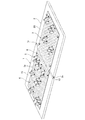
図1は、本発明の第1の実施形態に係る電気接続箱の一部展開斜視図である。図2は、図1のA−A’断面図であり、図3は、同電気接続箱の要部拡大図である。 FIG. 1 is a partially exploded perspective view of an electrical junction box according to the first embodiment of the present invention. 2 is a cross-sectional view taken along line A-A ′ of FIG. 1, and FIG. 3 is an enlarged view of a main part of the electric junction box.
樹脂等の絶縁材からなる第1及び第2のインシュレーションパネル1、2は、所定の隙間dを介して配されている。第1及び第2のインシュレーションパネルの片面(配線面1S、2S)には、一方の縁部1e、2eを介してまたぐように一枚のフレキシブル・フラット・ケーブル3が乗せられている。このフレキシブル・フラット・ケーブル3は、図2に示すように、導電材3aが絶縁材3bによって覆われており、所定の位置において絶縁材3bの上面が剥がされて導電材3aが露出したランド4が形成されている。なお、導電材3aは、例えば35μm〜400μmの任意の厚さの銅箔を用いることができる。このランド4上には、金属片を折り曲げることにより、上部に突出した板状の接続端子部5aと、この接続端子部5bを支える導体接続部5bとからなるL字形のタブ端子5が乗せられている。接続端子部5aは、後述する外部電装部品と電気的に接合し、導体接続部5bは、導電材3bと電気的に接合する。更に、第1及び第2のインシュレーションパネル1、2の四隅には、図3に示すような係止具6が設けられている。係止具6は、棒状の基部6aの上端から円周方向へ下向きに延びる押さえ部6bが形成されている。この係止具6は、フレキシブル・フラット・ケーブル3の所定の箇所に設けられた孔3cから突出し、フレキシブル・フラット・ケーブル3の四隅をインシュレーションパネル1(2)に押さえつけるようにして固定する。
The 1st and
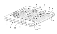
図4は、同電気接続箱の分解斜視図である。 FIG. 4 is an exploded perspective view of the electric junction box.
第1及び第2のインシュレーションパネル1、2は、間に絶縁材7を介して配線されていない背面同士が重なり合わせられる。上側の第1のインシュレーションパネル1の配線面側には、第1のインシュレーションパネル1と対向する方向に開口した箱状の上ケース8が配され、下側に配された第2のインシュレーションパネル2の配線面側には、上ケース8と脱着可能に係合する下ケース9が配される。ここで、上ケース8の上面には、ヒューズ10及びリレー11と脱着可能に係合するヒューズ装着部8a及びリレー装着部8bが一体形成されており、下ケース9の底面には、コネクタ12が脱着可能に係合するコネクタ装着部9aが一体成形されている。
As for the 1st and
次に、このように構成される電気接続箱の製造方法について説明する。 Next, the manufacturing method of the electrical junction box comprised in this way is demonstrated.
はじめに、[A]インシュレーションパネル1、2を、間隔dを介して配置した後、所定の位置にランド4が形成されたフレキシブル・フラット・ケーブル3を第1及び第2のインシュレーションパネル1、2にまたがるように乗せる。ここで、インシュレーションパネル1(2)に設置された係止具6は、フレキシブル・フラット・ケーブル3の四隅の孔3cに通す。次に、[B]図5に示すように、タブ端子5の導電材接続部5b上に第1の電極13と第2の電極14を所定の隙間を介して接触させ、加圧後通電して抵抗溶接を行う。続いて、[C]インシュレーションパネル1(2)の配線されていない背面同士を絶縁材8を介して重ね合わせ、[D]最後に、タブ端子5の接続端子部5aが外部電装部品係合部8a,8b(9a)に対応するように上下ケース8、9に収納する。なお、製造工程中の[B]のフレキシブル・フラット・ケーブル3の導電材3aとタブ端子5とを接続する方法として、抵抗溶接の他にもレーザ溶接、ハンダ付け及び超音波溶着のいずれかの方法を用いることができる。
First, after [A] the
このように電気接続箱を構成することで、電気接続箱を小型化することが可能となる。また、回路となる配線材はフラット配線材で構成されているため、容易に交換することができ回路設計の自由度が増す。 By configuring the electrical junction box in this way, the electrical junction box can be reduced in size. Moreover, since the wiring material used as a circuit is comprised with the flat wiring material, it can replace | exchange easily and the freedom degree of circuit design increases.
図6は、本発明に係る他の実施形態における電気接続箱の一部展開図であり、図7は、その収納時の一部斜視図である。 FIG. 6 is a partial development view of an electrical junction box according to another embodiment of the present invention, and FIG. 7 is a partial perspective view when the electrical connection box is stored.
この実施形態では、第1及び第2のインシュレーションパネル1、2の一方の縁部1e、2eの間には、第1の実施形態に加えてヒンジ13が設けられている。このようにヒンジ13を介することにより、位置合わせをしてインシュレーションパネル1、2の背面同士を合わせる必要もなく、また上下ケース8、9の内部においてインシュレーションパネル1、2を安定して固定することができる。
In this embodiment, a
図8及び図9は、本発明に係る他の電気接続箱の一部斜視図である。 8 and 9 are partial perspective views of other electrical junction boxes according to the present invention.
図8における実施例では、フレキシブル・フラット・ケーブル3に代えて、配線材としてフラットケーブル14が用いられており、図9における実施例では、配線材としてフレキシブルプリント基板15が用いられている。
In the embodiment in FIG. 8, a
このように様々なフラット配線材を用い、本発明を実施することができる。 Thus, the present invention can be implemented using various flat wiring materials.
1…第1のインシュレーションパネル、2…第2のインシュレーションパネル、3…フレキシブル・フラット・ケーブル、4,15…ランド、5…タブ端子、6…係止具、7…絶縁材、8…上ケース、9…下ケース、10…ヒューズ、11…リレー、12…コネクタ、13…ヒンジ、14…フラットケーブル、15…フレキシブルプリント基板。
DESCRIPTION OF
Claims (3)
前記第1及び第2の絶縁基板の配線面に沿って前記第1及び第2の絶縁基板を一方の縁部側からまたぐように敷設されたフラット配線材と、
前記第1及び第2の絶縁基板の端子収容部に前記配線面側に突出するように装着されると共に前記フラット配線材の導体と電気的に接続された端子と、
外面に前記端子の先端が臨むコネクタ部を有し内部に前記第1及び第2の絶縁基板を収容する上下ケースと
を備えたことを特徴とする電気接続箱。 A first insulating substrate having a wiring surface on which a flat wiring material is laid and a terminal accommodating portion formed, the wiring surfaces being disposed to face opposite sides of each other; and
A flat wiring material laid so as to straddle the first and second insulating substrates from one edge side along the wiring surfaces of the first and second insulating substrates;
A terminal mounted on the terminal accommodating portion of the first and second insulating substrates so as to protrude toward the wiring surface side and electrically connected to the conductor of the flat wiring material;
An electrical connection box, comprising: a connector portion on the outer surface facing the tip of the terminal; and an upper and lower case for accommodating the first and second insulating substrates therein.
Priority Applications (1)
| Application Number | Priority Date | Filing Date | Title |
|---|---|---|---|
| JP2005358077A JP2007166743A (en) | 2005-12-12 | 2005-12-12 | Electric connection box |
Applications Claiming Priority (1)
| Application Number | Priority Date | Filing Date | Title |
|---|---|---|---|
| JP2005358077A JP2007166743A (en) | 2005-12-12 | 2005-12-12 | Electric connection box |
Publications (1)
| Publication Number | Publication Date |
|---|---|
| JP2007166743A true JP2007166743A (en) | 2007-06-28 |
Family
ID=38249016
Family Applications (1)
| Application Number | Title | Priority Date | Filing Date |
|---|---|---|---|
| JP2005358077A Pending JP2007166743A (en) | 2005-12-12 | 2005-12-12 | Electric connection box |
Country Status (1)
| Country | Link |
|---|---|
| JP (1) | JP2007166743A (en) |
Cited By (1)
| Publication number | Priority date | Publication date | Assignee | Title |
|---|---|---|---|---|
| JP2011250569A (en) * | 2010-05-26 | 2011-12-08 | Auto Network Gijutsu Kenkyusho:Kk | Electric connection box |
-
2005
- 2005-12-12 JP JP2005358077A patent/JP2007166743A/en active Pending
Cited By (1)
| Publication number | Priority date | Publication date | Assignee | Title |
|---|---|---|---|---|
| JP2011250569A (en) * | 2010-05-26 | 2011-12-08 | Auto Network Gijutsu Kenkyusho:Kk | Electric connection box |
Similar Documents
| Publication | Publication Date | Title |
|---|---|---|
| JP4584600B2 (en) | Circuit structure | |
| JP2962160B2 (en) | Electrical junction box | |
| JP5422856B2 (en) | Electronic device housing with printed circuit board and method for manufacturing the electronic device housing | |
| US6512187B2 (en) | Lattice-shaped circuit board | |
| JP2005295724A (en) | Electric connection box | |
| JP2005295735A (en) | Electric connection box | |
| JP5307052B2 (en) | In-vehicle electrical junction box, and circuit material and circuit unit used therefor | |
| JP2002058132A (en) | Electric junction box | |
| JP2006304568A (en) | Electrical junction box | |
| JP2007166743A (en) | Electric connection box | |
| JP2002078144A (en) | Electric junction box | |
| WO2006006306A1 (en) | Interconnecting connector | |
| JP2007165059A (en) | Tab terminal, its flat wiring member connection structure, and electric connection box | |
| JP3976627B2 (en) | Manufacturing method of electrical junction box | |
| JP2006325301A (en) | Circuit component | |
| JP2007166741A (en) | Electrical connection box | |
| JP2007165058A (en) | Tab terminal, its fastening structure, its connecting structure, and electric connection box | |
| JP3307340B2 (en) | Circuit board and electrical junction box containing the circuit board | |
| JP2000209742A (en) | Electric circuit material and electrical junction box provided with the same | |
| JP2002078158A (en) | Assembling method for electric junction box | |
| JP2007166742A (en) | Method of manufacturing electric connection box | |
| JP2002078150A (en) | Electric junction box | |
| JP2000092656A (en) | Electrical connection box | |
| JP2000125445A (en) | Circuit board, junction box with the circuit board, and manufacture of the circuit board | |
| JP3637855B2 (en) | How to change the specifications of the electrical junction box |