JP2010211048A - Method of driving electrohoretic display device, electrohoretic display device, and electronic device - Google Patents
Method of driving electrohoretic display device, electrohoretic display device, and electronic device Download PDFInfo
- Publication number
- JP2010211048A JP2010211048A JP2009058284A JP2009058284A JP2010211048A JP 2010211048 A JP2010211048 A JP 2010211048A JP 2009058284 A JP2009058284 A JP 2009058284A JP 2009058284 A JP2009058284 A JP 2009058284A JP 2010211048 A JP2010211048 A JP 2010211048A
- Authority
- JP
- Japan
- Prior art keywords
- display
- potential
- pixel
- common electrode
- display device
- Prior art date
- Legal status (The legal status is an assumption and is not a legal conclusion. Google has not performed a legal analysis and makes no representation as to the accuracy of the status listed.)
- Pending
Links
Images


Abstract
Description
本発明は、電気泳動表示装置の駆動方法、電気泳動表示装置、及び電子機器に関するものである。 The present invention relates to an electrophoretic display device driving method, an electrophoretic display device, and an electronic apparatus.
溶液中に電気泳動粒子を分散させてなる分散液に電界を印加した際に、クーロン力によって電気泳動粒子が泳動する現象(電気泳動現象)が知られており、当該現象を利用した電気泳動表示装置が開発されている。このような電気泳動表示装置は、例えば、下記特許文献1,2に開示されている。電気泳動表示装置は、共通電極と複数に分割された画素電極との間に電位差を生じさせることにより、表示色を所望の色に変化させることが可能となる。特許文献1記載の駆動方法では、共通電極に周期的にローレベルとハイレベルとを繰り返すパルス波を入力する駆動方法(コモン振り駆動)を採用していた。
When an electric field is applied to a dispersion liquid in which electrophoretic particles are dispersed in a solution, a phenomenon (electrophoresis phenomenon) in which the electrophoretic particles migrate due to Coulomb force is known. Electrophoretic display using this phenomenon Equipment has been developed. Such an electrophoretic display device is disclosed, for example, in
ところで、電気泳動表示装置に限らず、表示装置一般においては、その表示解像度は画素サイズ及び画素ピッチにより規定され、表示される線幅は1画素単位の幅に固定されている。近年では、アンチエイリアス処理などの画像処理を施すことで擬似的に線幅を調整することが成されているが、表示装置単体で線幅調整を可能にすることは検討されていなかった。 By the way, not only in an electrophoretic display device but in a display device in general, the display resolution is defined by the pixel size and the pixel pitch, and the displayed line width is fixed to the width of one pixel unit. In recent years, it has been possible to artificially adjust the line width by performing image processing such as anti-aliasing, but it has not been studied to enable line width adjustment by a single display device.
本発明は、上記事情に鑑み成されたものであって、表示装置単体での線幅調整を可能とし、表現力を向上させることができる電気泳動表示装置の駆動方法、及び電気泳動表示装置を提供することを目的の一つとする。 The present invention has been made in view of the above circumstances, and provides an electrophoretic display device driving method and an electrophoretic display device capable of adjusting the line width of a display device alone and improving expressive power. One of the purposes is to provide.
本発明の電気泳動表示装置の駆動方法は、第1基板と第2基板との間に電気泳動粒子を含む電気泳動素子を挟持してなり、複数の画素を配列してなる表示部を備え、各々の前記画素に対応して前記第1基板の前記電気泳動素子側に形成された画素電極と、前記第2基板の前記電気泳動素子側に形成され、複数の前記第1電極と対向する共通電極とを有する電気泳動表示装置の駆動方法であって、前記画素電極に第1又は第2の電位を入力する一方、前記共通電極に前記第1の電位と前記第2の電位とを周期的に繰り返すパルス波を入力し、前記共通電極の電位が特定階調を表示する電位であるときに前記パルス波の入力を停止することで、前記表示部に、前記特定階調からなる画像要素の輪郭が拡張された画像を表示することを特徴とする。 The driving method of the electrophoretic display device of the present invention includes a display unit in which an electrophoretic element including electrophoretic particles is sandwiched between a first substrate and a second substrate, and a plurality of pixels are arranged. A pixel electrode formed on the electrophoretic element side of the first substrate corresponding to each pixel, and a common electrode formed on the electrophoretic element side of the second substrate and facing the plurality of first electrodes A method of driving an electrophoretic display device having electrodes, wherein the first potential and the second potential are periodically input to the common electrode while the first potential or the second potential is input to the pixel electrode. When the pulse wave to be repeated is input, and the potential of the common electrode is a potential for displaying a specific gradation, the input of the pulse wave is stopped, so that an image element having the specific gradation is displayed on the display unit. An image with an extended outline is displayed.
この駆動方法では、共通電極に第1の電位と第2の電位とを周期的に繰り返すパルス波を入力することで電気泳動素子を駆動する、いわゆるコモン振り駆動を採用している。そして、コモン振り駆動における共通電極への電位入力停止のタイミングを、上記特定階調を表示する電位とすることで、特定階調からなる画像要素の輪郭を拡張することを可能にしたものである。 This driving method employs so-called common swing driving in which the electrophoretic element is driven by inputting a pulse wave that periodically repeats the first potential and the second potential to the common electrode. The timing of stopping the potential input to the common electrode in the common swing drive is set to the potential for displaying the specific gradation, thereby making it possible to extend the contour of the image element having the specific gradation. .
コモン振り駆動では、共通電極が第1の電位である期間に、第2の電位に保持された画素電極との間の電気泳動素子を駆動し、共通電極が第2の電位である期間に、第1の電位に保持された画素電極との間の電気泳動素子を駆動する。したがって、共通電極が第1の電位である期間には、第2の電位に保持された画素電極が属する画素は実質的に動作せず、共通電極が第2の電位である期間には、第1の電位に保持された画素電極が属する画素は実質的に動作しない。 In the common swing drive, the electrophoretic element between the pixel electrode held at the second potential is driven in a period in which the common electrode is at the first potential, and in the period in which the common electrode is at the second potential, The electrophoretic element between the pixel electrode held at the first potential is driven. Therefore, during the period when the common electrode is at the first potential, the pixel to which the pixel electrode held at the second potential belongs does not substantially operate, and during the period when the common electrode is at the second potential, A pixel to which a pixel electrode held at a potential of 1 belongs substantially does not operate.
また、共通電極は画素電極よりも大きい平面領域を有し、複数の画素電極と対向しているため、動作時に画素電極と共通電極との間に形成される電界は、画素電極側で狭く、共通電極に近づくに従って広がった電界となる。 In addition, since the common electrode has a larger planar area than the pixel electrode and faces the plurality of pixel electrodes, an electric field formed between the pixel electrode and the common electrode during operation is narrow on the pixel electrode side, The electric field spreads as it approaches the common electrode.
以上から、電気泳動表示装置をコモン振り駆動した場合には、第1の電位に保持された画素電極(以下第1画素電極とする)と、第2の電位に保持された画素電極(以下第2画素電極とする)とが隣り合う領域において、共通電極の電位変化に伴って、第1画素電極から第2画素電極上にまで広がる電界が形成される期間と、第2画素電極から第1画素電極上にまで広がる電界が形成される期間とが交互に繰り返される。 From the above, when the electrophoretic display device is driven in a common manner, the pixel electrode held at the first potential (hereinafter referred to as the first pixel electrode) and the pixel electrode held at the second potential (hereinafter referred to as the first electrode). In a region adjacent to the second pixel electrode), a period in which an electric field extending from the first pixel electrode to the second pixel electrode is formed in accordance with the potential change of the common electrode, and from the second pixel electrode to the first The period in which the electric field extending to the pixel electrode is formed is alternately repeated.
そして、電気泳動素子に含まれる電気泳動粒子は、上述した電界に沿って移動するため、第1画素電極の属する画素が動作する期間では、第1画素電極の電位に対応した表示が第1画素電極よりも広い領域に及ぶ。逆に、第2画素電極の属する画素が動作する期間では、第2画素電極の電位に対応した表示が第2画素電極よりも広い領域に及ぶ。 Since the electrophoretic particles contained in the electrophoretic element move along the above-described electric field, the display corresponding to the potential of the first pixel electrode is displayed in the first pixel during the period in which the pixel to which the first pixel electrode belongs is operating. It covers a wider area than the electrode. Conversely, during the period in which the pixel to which the second pixel electrode belongs operates, the display corresponding to the potential of the second pixel electrode covers a wider area than the second pixel electrode.
本発明の駆動方法は、上の作用を利用し、共通電極への電位入力停止のタイミングを適切に制御することで、特定階調からなる画像要素の輪郭を自在に拡張させて表示できるようにしたものである。この駆動方法によれば、線幅の調整を表示装置単体で行うことができ、表現力に優れた表示が可能になる。 The driving method of the present invention can display the image element having a specific gradation by freely expanding the outline by appropriately controlling the timing of stopping the potential input to the common electrode by using the above-described action. It is a thing. According to this driving method, the line width can be adjusted by a single display device, and a display with excellent expressive power is possible.
前記パルス波の最終パルスにおける後半のパルス幅を、前記パルス波を構成する他のパルスのパルス幅よりも大きくすることが好ましい。
この駆動方法によれば、線幅を規定する最後の電圧印加期間を長くするので、より確実に輪郭が拡張された表示を得ることができる。
It is preferable that the pulse width of the latter half of the last pulse of the pulse wave is larger than the pulse width of other pulses constituting the pulse wave.
According to this driving method, since the last voltage application period that defines the line width is lengthened, it is possible to obtain a display with a more expanded contour.
前記パルス波の最終パルスの周期を、前記パルス波を構成する他のパルスの周期よりも長くすることが好ましい。
この駆動方法によれば、線幅を規定する最後の電圧印加期間を長くすることで、より確実に輪郭が拡張された表示を得ることができる。さらに、画素電極及び共通電極と電気泳動素子とに対して異なる極性の電位が入力期間を均一化することができる。これにより、電極や電気泳動素子の劣化を抑えることができる。
It is preferable that the period of the last pulse of the pulse wave is longer than the period of other pulses constituting the pulse wave.
According to this driving method, by extending the last voltage application period that defines the line width, it is possible to obtain a display with a more expanded contour. Furthermore, potentials having different polarities with respect to the pixel electrode and the common electrode and the electrophoretic element can make the input period uniform. Thereby, deterioration of an electrode or an electrophoretic element can be suppressed.
前記パルス幅又は前記周期の長さによって前記輪郭の拡張幅を調整することが好ましい。
この駆動方法によれば、パルス幅又は周期を調整するという簡便な操作で、輪郭の拡張幅を調整でき、さらに表現力に優れた表示を得ることができる。
It is preferable that the extension width of the contour is adjusted according to the pulse width or the length of the period.
According to this driving method, it is possible to adjust the extended width of the contour by a simple operation of adjusting the pulse width or the cycle, and it is possible to obtain a display with excellent expressive power.
前記特定階調が、階調値が最大である第1の階調、又は階調値が最小である第2の階調であることが好ましい。
この駆動方法によれば、例えば黒表示された画像要素の輪郭を拡張した表示、あるいは、白表示された画像要素の輪郭を拡張した表示が可能である。
The specific gradation is preferably a first gradation having a maximum gradation value or a second gradation having a minimum gradation value.
According to this driving method, for example, display in which the outline of an image element displayed in black is expanded or display in which the outline of an image element displayed in white is expanded is possible.
前記特定階調が、中間階調であることも好ましい。
この駆動方法によれば、例えばグレー表示された画像要素の輪郭を拡張した表示も可能である。
It is also preferable that the specific gradation is an intermediate gradation.
According to this driving method, for example, display in which the outline of an image element displayed in gray is expanded is also possible.
本発明の電気泳動表示装置は、第1基板と第2基板との間に電気泳動粒子を含む電気泳動素子を挟持してなり、複数の画素を配列してなる表示部を備え、各々の前記画素に対応して前記第1基板の前記電気泳動素子側に形成された画素電極と、前記第2基板の前記電気泳動素子側に形成され、複数の前記第1電極と対向する共通電極と、前記画素電極及び前記共通電極に入力する電位を制御する制御部と、を有する電気泳動表示装置であって、前記制御部は、前記画素電極に第1又は第2の電位を入力する一方、前記共通電極に前記第1の電位と前記第2の電位とを周期的に繰り返すパルス波を入力し、前記共通電極の電位が特定階調を表示する電位であるときに前記パルス波の入力を停止することで、前記表示部に、前記特定階調からなる画像要素の輪郭が拡張された画像を表示することを特徴とする。 An electrophoretic display device of the present invention includes a display unit in which an electrophoretic element including electrophoretic particles is sandwiched between a first substrate and a second substrate, and a plurality of pixels are arranged. A pixel electrode formed on the side of the electrophoretic element of the first substrate corresponding to the pixel, a common electrode formed on the side of the electrophoretic element of the second substrate and facing the plurality of first electrodes, A control unit that controls a potential input to the pixel electrode and the common electrode, wherein the control unit inputs the first or second potential to the pixel electrode, A pulse wave that periodically repeats the first potential and the second potential is input to the common electrode, and the input of the pulse wave is stopped when the potential of the common electrode is a potential that displays a specific gradation. As a result, the display unit has the specific gradation. The contour of the image element and displaying the expanded image.
この構成によれば、共通電極への電位入力停止のタイミングを適切に制御することで、特定階調からなる画像要素の輪郭を自在に拡張させて表示することができる。したがって、線幅の調整を表示装置単体で行うことができ、表現力に優れた表示が可能な電気泳動表示装置を実現することができる。 According to this configuration, by appropriately controlling the timing of stopping the potential input to the common electrode, it is possible to freely expand and display the contour of the image element having a specific gradation. Therefore, the line width can be adjusted by a single display device, and an electrophoretic display device capable of displaying with excellent expressive power can be realized.
前記パルス波の最終パルスにおける後半のパルス幅が、前記パルス波を構成する他のパルスのパルス幅よりも大きいことが好ましい。
この構成によれば、線幅を規定する最後の電圧印加期間が長くなるので、より確実に輪郭が拡張された表示を得ることができる。
It is preferable that a pulse width of the latter half of the last pulse of the pulse wave is larger than a pulse width of other pulses constituting the pulse wave.
According to this configuration, since the last voltage application period that defines the line width becomes longer, it is possible to obtain a display with a more expanded contour.
前記パルス波の最終パルスの周期が、前記パルス波を構成する他のパルスの周期よりも長いことが好ましい。
この構成によれば、線幅を規定する最後の電圧印加期間が長くなるので、より確実に輪郭が拡張された表示を得ることができる。さらに、画素電極及び共通電極と電気泳動素子とに対して異なる極性の電位が入力期間を均一化することができる。これにより、電極や電気泳動素子の劣化を抑えることができる。
It is preferable that the period of the last pulse of the pulse wave is longer than the period of other pulses constituting the pulse wave.
According to this configuration, since the last voltage application period that defines the line width becomes longer, it is possible to obtain a display with a more expanded contour. Furthermore, potentials having different polarities with respect to the pixel electrode and the common electrode and the electrophoretic element can make the input period uniform. Thereby, deterioration of an electrode or an electrophoretic element can be suppressed.
前記制御部は、前記パルス幅又は前記周期の長さによって前記輪郭の拡張幅を調整する構成とすることもできる。
この構成によれば、パルス幅又は周期を調整するという簡便な操作で、輪郭の拡張幅を調整でき、さらに表現力に優れた表示を得ることができる電気泳動表示装置となる。
The control unit may be configured to adjust an extension width of the contour according to the pulse width or the length of the cycle.
According to this configuration, an electrophoretic display device that can adjust the extended width of the contour with a simple operation of adjusting the pulse width or cycle and obtain a display with excellent expressive power can be obtained.
前記特定階調が、階調値が最大である第1の階調、又は階調値が最小である第2の階調であることが好ましい。
この構成によれば、例えば黒表示された画像要素の輪郭を拡張した表示、あるいは、白表示された画像要素の輪郭を拡張した表示が可能である。
The specific gradation is preferably a first gradation having a maximum gradation value or a second gradation having a minimum gradation value.
According to this configuration, for example, display in which the outline of an image element displayed in black is expanded or display in which the outline of an image element displayed in white is expanded is possible.
前記特定階調が、中間階調であることも好ましい。
この構成によれば、例えばグレー表示された画像要素の輪郭を拡張した表示も可能である。
It is also preferable that the specific gradation is an intermediate gradation.
According to this configuration, for example, display in which the outline of an image element displayed in gray is expanded is also possible.
本発明の電子機器は、先に記載の電気泳動表示装置を備えたことを特徴とする。
この構成によれば、表現力に優れた表示手段を具備した電子機器を提供することができる。
An electronic apparatus according to the present invention includes the electrophoretic display device described above.
According to this configuration, it is possible to provide an electronic device including a display unit having excellent expressive power.
以下、図面を参照しつつ本発明の電気泳動表示装置について説明する。
なお、本発明の範囲は、以下の実施の形態に限定されるものではなく、本発明の技術的思想の範囲内で任意に変更可能である。また、以下の図面においては、各構成をわかりやすくするために、実際の構造と各構造における縮尺や数等を異ならせている。
The electrophoretic display device of the present invention will be described below with reference to the drawings.
The scope of the present invention is not limited to the following embodiment, and can be arbitrarily changed within the scope of the technical idea of the present invention. Moreover, in the following drawings, in order to make each configuration easy to understand, the actual structure is different from the scale and number of each structure.
(第1の実施形態)
図1は、本発明の第1の実施の形態に係る電気泳動表示装置100の概略構成図である。図2(a)は、電気泳動表示装置100の断面構造とともに電気的構成を示した図である。
(First embodiment)
FIG. 1 is a schematic configuration diagram of an
電気泳動表示装置100は、複数の画素(セグメント)40が配置された表示部5と、コントローラー(制御部)63と、コントローラー63と接続された画素電極駆動回路60とを備えている。画素電極駆動回路60は、それぞれの画素40と画素電極配線61を介して接続されている。また、表示部5には、各々の画素40に共通の共通電極37(図2参照)が設けられている。なお、図1では共通電極37を便宜的に配線として表示している。
The
電気泳動表示装置100は、コントローラー63から画素電極駆動回路60に画像データを転送し、かかる画像データに基づく電位を、個々の画素40に直接入力するセグメント駆動方式の電気泳動表示装置である。
The
図2(a)に示すように、電気泳動表示装置100の表示部5は、第1基板30と第2基板31との間に、電気泳動素子32を挟持した構成である。第1基板30の電気泳動素子32側に複数の画素電極(セグメント電極)35が形成され、第2基板31の電気泳動素子32側には共通電極37が形成されている。電気泳動素子32は、電気泳動粒子を内部に封入した複数のマイクロカプセル20を平面的に配列した構成である。電気泳動表示装置100は、電気泳動素子32により形成された画像を共通電極37側に表示する。
As shown in FIG. 2A, the
第1基板30は、ガラスやプラスチック等からなる基板であり、画像表示面とは反対側に配置されるため透明なものでなくてもよい。画素電極35は、Cu(銅)箔上にニッケルメッキと金メッキとをこの順番で積層したものや、Al(アルミニウム)、ITO(インジウム・スズ酸化物)などを用いて形成される。
第2基板31は、ガラスやプラスチック等からなる基板であり、画像表示側に配置されるため透明基板とされる。共通電極37は、MgAg(マグネシウム銀)、ITO、IZO(登録商標;インジウム・亜鉛酸化物)などを用いて形成される透明電極である。
The
The
各々の画素電極35には、画素電極配線61を介して画素電極駆動回路60が接続されている。画素電極駆動回路60には、各々の画素電極配線61に対応するスイッチング素子60sが設けられており、スイッチング素子60sの動作により画素電極35に対する電位の入力と電気的切断(ハイインピーダンス化)を行う。
一方、共通電極37には、共通電極配線62を介して共通電極駆動回路64が接続されている。共通電極駆動回路64には、共通電極配線62と接続されたスイッチング素子64sが設けられており、スイッチング素子64sの動作により共通電極37に対する電位の入力と電気的切断(ハイインピーダンス化)を行う。
A pixel
On the other hand, a common
なお、電気泳動素子32は、あらかじめ第2基板31側に形成され、接着剤層33までを含めた電気泳動シートとして取り扱われるのが一般的である。製造工程において、電気泳動シートは接着剤層33の表面に保護用の剥離シートが貼り付けられた状態で取り扱われる。そして、別途製造された第1基板30(画素電極35などが形成されている)に対して、剥離シートを剥がした当該電気泳動シートを貼り付けることによって、表示部5を形成する。このため、接着剤層33は画素電極35側のみに存在することになる。
In general, the
図2(b)は、マイクロカプセル20の模式断面図である。マイクロカプセル20は、例えば30〜50μm程度の粒径を有しており、内部に分散媒21と、複数の白色粒子(電気泳動粒子)27と、複数の黒色粒子(電気泳動粒子)26とを封入した球状体である。マイクロカプセル20は、図2に示したように共通電極37と画素電極35との間に挟持され、1つの画素40内に1つ又は複数のマイクロカプセル20が配置される。
FIG. 2B is a schematic cross-sectional view of the
マイクロカプセル20の外殻部(壁膜)は、ポリメタクリル酸メチル、ポリメタクリル酸エチルなどのアクリル樹脂、ユリア樹脂、アラビアガムなどの透光性を持つ高分子樹脂などを用いて形成される。
分散媒21は、白色粒子27と黒色粒子26とをマイクロカプセル20内に分散させる液体である。分散媒21としては、水、アルコール系溶媒(メタノール、エタノール、イソプロパノール、ブタノール、オクタノール、メチルセルソルブなど)、エステル類(酢酸エチル、酢酸ブチルなど)、ケトン類(アセトン、メチルエチルケトン、メチルイソブチルケトンなど)、脂肪族炭化水素(ぺンタン、ヘキサン、オクタンなど)、脂環式炭化水素(シクロへキサン、メチルシクロへキサンなど)、芳香族炭化水素(ベンゼン、トルエン、長鎖アルキル基を有するベンゼン類(キシレン、ヘキシルベンゼン、ヘブチルベンゼン、オクチルベンゼン、ノニルベンゼン、デシルベンゼン、ウンデシルベンゼン、ドデシルベンゼン、トリデシルベンゼン、テトラデシルベンゼンなど))、ハロゲン化炭化水素(塩化メチレン、クロロホルム、四塩化炭素、1,2−ジクロロエタンなど)、カルボン酸塩などを例示することができ、その他の油類であってもよい。これらの物質は単独又は混合物として用いることができ、さらに界面活性剤などを配合してもよい。
The outer shell portion (wall film) of the
The
白色粒子27は、例えば、二酸化チタン、亜鉛華、三酸化アンチモン等の白色顔料からなる粒子(高分子あるいはコロイド)であり、例えば負に帯電されて用いられる。黒色粒子26は、例えば、アニリンブラック、カーボンブラック等の黒色顔料からなる粒子(高分子あるいはコロイド)であり、例えば正に帯電されて用いられる。
これらの顔料には、必要に応じ、電解質、界面活性剤、金属石鹸、樹脂、ゴム、油、ワニス、コンパウンドなどの粒子からなる荷電制御剤、チタン系カップリング剤、アルミニウム系カップリング剤、シラン系カップリング剤等の分散剤、潤滑剤、安定化剤などを添加することができる。
また、黒色粒子26及び白色粒子27に代えて、例えば赤色、緑色、青色などの顔料を用いてもよい。かかる構成によれば、表示部5に赤色、緑色、青色などを表示することができる。
The
These pigments include electrolytes, surfactants, metal soaps, resins, rubbers, oils, varnishes, compound charge control agents, titanium-based coupling agents, aluminum-based coupling agents, silanes as necessary. A dispersant such as a system coupling agent, a lubricant, a stabilizer, and the like can be added.
Further, instead of the
図3は、電気泳動素子の動作説明図である。図3(a)は、画素40を白表示する場合、図3(b)は、画素40を黒表示する場合をそれぞれ示している。
図3(a)に示す白表示の場合には、共通電極37が相対的に高電位、画素電極35が相対的に低電位に保持される。これにより、負に帯電した白色粒子27が共通電極37に引き寄せられる一方、正に帯電した黒色粒子26が画素電極35に引き寄せられる。その結果、表示面側となる共通電極37側からこの画素を見ると、白色(W)が認識される。
図3(b)に示す黒表示の場合、共通電極37が相対的に低電位、画素電極35が相対的に高電位に保持される。これにより、正に帯電した黒色粒子26が共通電極37に引き寄せられる一方、負に帯電した白色粒子27が画素電極35に引き寄せられる。その結果、共通電極37側からこの画素を見ると黒色(B)が認識される。
FIG. 3 is an operation explanatory diagram of the electrophoretic element. 3A shows a case where the
In the case of white display shown in FIG. 3A, the
In the case of black display shown in FIG. 3B, the
[第1の駆動方法(太い黒線の表示方法)]
次に、上記構成を備えた電気泳動表示装置の駆動方法について説明する。
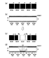
図4は、本発明に係る電気泳動表示装置の第1の駆動方法による画素40の状態遷移を示す説明図である。図4(a)及び図4(b)は、5つの画素40の初期状態を示す平面図及び断面図である。図4(c)及び図4(d)は、書き込み動作後の画素40の状態を示す平面図及び断面図である。図5は、第1の駆動方法におけるタイミングチャートである。
[First driving method (displaying thick black lines)]
Next, a driving method of the electrophoretic display device having the above configuration will be described.
FIG. 4 is an explanatory diagram showing state transition of the
本実施形態に係る第1の駆動方法は、図4(a)に示す白表示された5つの画素40のうち、画素電極SEG0(画素電極35)が属する中央の画素40のみを、図4(c)に示すように黒表示(特定階調)に移行させ、かつ、1画素の幅よりも広い領域を黒表示させる駆動方法である。以下、かかる駆動方法について詳細に説明する。
In the first driving method according to the present embodiment, only the
図4(a)及び図4(b)に示す白表示の画素40では、画素電極SEG0、SEG1側に黒色粒子26が引き寄せられ、共通電極37側に白色粒子27が引き寄せられている。かかる表示状態に移行させる駆動方法としては、例えば、2つの画素電極SEG0、SEG1にローレベル(例えば0V)の電位を入力し、共通電極COM(共通電極37)にローレベルの電位とハイレベル(例えば15V)の電位を周期的に繰り返すパルス波を入力する。これにより、5つの画素40をいずれも白表示状態とすることができる。また、共通電極COMをハイレベルの電位に保持しても同様の表示状態を得ることができる。
In the
なお、図4(a)に示す初期状態は、説明の簡単のために、全ての画素40が白表示されている状態を示したにすぎない。すなわち、本実施形態の駆動方法において、表示を更新する前の初期状態は任意の表示状態とすることができる。例えば、5つの画素40が全て黒表示されている状態を初期状態としてもよく、白表示の画素40と黒表示の画素40が混在した状態を初期状態としてもよい。
Note that the initial state shown in FIG. 4A merely shows a state in which all the
次に、図4(a)に示す白表示状態から図4(c)に示す白表示と黒表示とが混在した状態とするには、図5(a)に示すように、画素電極SEG0にハイレベル(15V)の電位を入力する一方、画素電極SEG1にローレベル(例えば0V)の電位を入力する。そして、共通電極COMに、ローレベル(例えば0V)とハイレベル(例えば15V)を周期的に繰り返す矩形波状のパルス波を入力する。 Next, in order to change from the white display state shown in FIG. 4A to the state where the white display and the black display shown in FIG. 4C are mixed, the pixel electrode SEG0 is applied to the pixel electrode SEG0 as shown in FIG. While a high level (15V) potential is input, a low level (for example, 0V) potential is input to the pixel electrode SEG1. Then, a rectangular wave pulse wave that periodically repeats a low level (for example, 0 V) and a high level (for example, 15 V) is input to the common electrode COM.
これにより、画素電極SEG0が属する画素40では、共通電極COMがローレベルである期間に、画素電極SEG0(ハイレベル)と共通電極COMとの電位差により電気泳動素子32が駆動され、画素40が黒表示動作する。
一方、画素電極SEG1が属する画素40では、共通電極COMがハイレベルである期間に画素電極SEG1と共通電極COMとの間に電位差が生じ、白表示動作する。しかし、これらの画素40は、初期状態がいずれも白表示であるため表示は変化しない。
Thereby, in the
On the other hand, in the
ここで、本実施形態の駆動方法では、図5(a)に示すように、共通電極COMに入力されるパルス波のうち最終パルスPnが、他のパルスとは異なるパルス幅のパルスとされている。より詳細には、最終パルスPn以外のパルスがデューティ比1:1、パルス幅Pw1のパルスであるのに対して、最終パルスPnは、後半のパルス幅が大きいデューティ比(例えば1:3)に設定されており、前半のパルス幅Pw1に対して、後半のパルス幅Pw2が大きくされている。 Here, in the driving method of the present embodiment, as shown in FIG. 5A, the final pulse Pn among the pulse waves input to the common electrode COM is a pulse having a pulse width different from that of the other pulses. Yes. More specifically, pulses other than the final pulse Pn are pulses having a duty ratio of 1: 1 and a pulse width Pw1, whereas the final pulse Pn has a duty ratio (eg, 1: 3) having a large pulse width in the latter half. The latter pulse width Pw2 is set larger than the first pulse width Pw1.
図4(d)に示すように、画素電極SEG0の属する画素40が黒表示動作する際には、画素電極SEG0よりも共通電極COMの方が広いため、画素電極SEG0から共通電極COMに向かう電界Eは、画素電極SEG0の端部から外側に広がるようにして形成される。一方、画素40が白表示動作する際には、画素電極SEG1から画素電極SEG0上の一部にまで広がった電界が形成される。
As shown in FIG. 4D, when the
すなわち、画素電極SEG0の属する画素40による黒表示領域は、共通電極COMの電位がハイレベルとローレベルとの間で切り替わるのに連動して変化する。そして、上記黒表示領域の広さ(線幅)は、共通電極COMへの電位入力が停止されたときの電界の状態に依存して決定される。つまり、共通電極COMへの電位入力を停止するタイミングにおける共通電極COMの電位により決定される。
That is, the black display region by the
そして、本実施形態では、画素電極SEG0の属する画素40により表示される線幅を拡張するために、共通電極COMへの電位入力停止のタイミングが、図5(a)に示すように、共通電極COMがローレベルである期間に設定されている。これにより、図4(d)に示したように、黒表示の領域を拡張しうる電界Eが形成されているときに電気泳動素子32への電圧印加を停止し、輪郭が拡張された表示が保持されるようにしている。
In this embodiment, in order to expand the line width displayed by the
さらに本実施形態の駆動方法では、共通電極COMに入力される最終パルスPnの後半部分のパルス幅が長くなっているため、パルス幅Pw1である他のパルスが入力されたときよりも、図4(d)に示す斜め方向の電界が電気泳動粒子に作用する時間が長くなる。
そのため、画素電極SEG0よりも広い範囲で黒色粒子26が共通電極COM側に引き寄せられ、図4(c)に示すように、画素電極SEG0の端部から外側に黒表示領域が拡張された表示を得ることができる。
Furthermore, in the driving method of the present embodiment, since the pulse width of the second half portion of the final pulse Pn input to the common electrode COM is longer, the pulse width Pw1 than when another pulse is input is shown in FIG. The time during which the oblique electric field shown in (d) acts on the electrophoretic particles becomes longer.
Therefore, the
さらにまた、本実施形態の駆動方法によれば、最終パルスPnの後半のパルス幅Pw2を調整することで、黒表示領域の拡張幅Wbを調整することが可能である。具体的には、パルス幅Pw2の長さを伸縮することで、拡張幅Wbを伸縮させることができる。これは、図4(d)に示すように、画素電極SEG0の端部から斜め方向に延びる電界は、画素電極SEG0から電極法線方向に形成される電界に比して弱く、またかかる斜め電界により移動される電気泳動粒子の移動距離も長くなるためである。 Furthermore, according to the driving method of the present embodiment, it is possible to adjust the expansion width Wb of the black display region by adjusting the pulse width Pw2 of the latter half of the final pulse Pn. Specifically, the expansion width Wb can be expanded and contracted by expanding and contracting the length of the pulse width Pw2. As shown in FIG. 4D, the electric field extending in the oblique direction from the end of the pixel electrode SEG0 is weaker than the electric field formed in the electrode normal direction from the pixel electrode SEG0. This is because the moving distance of the electrophoretic particles moved by is increased.
そのため、パルス幅Pw2を短くすると、画素電極SEG0側から離れた位置の共通電極COM近傍までは黒色粒子26が到達できなくなり、拡張幅Wbが狭くなる。逆に、パルス幅Pw2を長くすると、斜め電界により移動される黒色粒子26を共通電極COM近傍に到達させることができ、拡張幅Wbを広くすることができる。
Therefore, when the pulse width Pw2 is shortened, the
なお、図4(d)に示す電界Eが広がる領域には限界があるため、パルス幅Pw2の長さを一定時間以上に長くすると、拡張幅Wbは変化しなくなる。拡張幅Wbを調整できる範囲は、電気泳動表示装置100の構造や電気泳動素子32の特性にも依存するが、おおよそ0.5画素分である。したがって、本実施形態の駆動方法によれば、1画素分からおおよそ2画素分までの間で自在に線幅を調整することが可能である。
Since the region where the electric field E shown in FIG. 4D spreads is limited, the extension width Wb does not change when the pulse width Pw2 is made longer than a certain time. The range in which the expansion width Wb can be adjusted is approximately 0.5 pixels, although it depends on the structure of the
また本実施形態では、パルス幅Pw2をパルス幅Pw1よりも大きくした場合について説明したが、先に記載のように、共通電極COMへの電位入力停止のタイミングを適切に規定すれば、線幅を拡張する効果を得ることができる。そのため、パルス幅Pw2とパルス幅Pw1とが同等の長さとされていてもよい。したがって、パルス幅Pw2の下限値はPw1であり、上限値は拡張幅Wbが変化しなくなる長さである。 In this embodiment, the case where the pulse width Pw2 is larger than the pulse width Pw1 has been described. However, as described above, if the timing of stopping the potential input to the common electrode COM is appropriately defined, the line width is reduced. An expansion effect can be obtained. Therefore, the pulse width Pw2 and the pulse width Pw1 may be the same length. Therefore, the lower limit value of the pulse width Pw2 is Pw1, and the upper limit value is a length at which the extension width Wb does not change.
また、本発明の駆動方法では、図5(b)に示すタイミングチャートを採用することがより好ましい。図5(b)に示すタイミングチャートでは、共通電極COMに入力される最終パルスPnが前半後半ともにパルス幅Pw2のパルスとされている。すなわち、パルスの前半のパルス幅も他のパルスのパルス幅よりも長くされ、デューティ比1:1に変更されている。 In the driving method of the present invention, it is more preferable to employ the timing chart shown in FIG. In the timing chart shown in FIG. 5B, the last pulse Pn input to the common electrode COM is a pulse having a pulse width Pw2 in both the first half and the second half. That is, the pulse width of the first half of the pulse is also longer than the pulse width of the other pulses, and the duty ratio is changed to 1: 1.
図5(b)に示すタイミングチャートを採用することで、電気泳動素子32や画素電極35、共通電極37の劣化を抑えることができる。
より詳しくは、図5(a)に示した最終パルスPnでは、画素電極SEG0の属する画素40を黒表示動作させる期間が、同じ画素40を白表示させる期間よりも長くなる。また、画素電極SEG1の属する画素40を白表示動作させる期間が、同じ画素40を黒表示動作させる期間よりも長くなる。このように電気泳動素子32に作用する電界に偏りを生じると、画素電極35や共通電極37が電気化学的反応により劣化するおそれがあり、電気泳動素子32の寿命が短くなるおそれもある。
これに対して、図5(b)に示すタイミングチャートでは、最終パルスPnのデューティ比が1:1になっているため、電気泳動素子32に作用させる電界の偏りが生じることがなく、上記のような電気泳動素子32や電極の劣化が生じるのを回避し、長期間にわたって良好な表示を得ることができる。
By adopting the timing chart shown in FIG. 5B, deterioration of the
More specifically, in the final pulse Pn shown in FIG. 5A, the period during which the
On the other hand, in the timing chart shown in FIG. 5B, since the duty ratio of the final pulse Pn is 1: 1, the bias of the electric field applied to the
[第2の駆動方法(太い白線の表示方法)]
次に、本実施形態の第2の駆動方法について説明する。
図6は、本発明に係る電気泳動表示装置の第2の駆動方法による画素40の状態遷移を示す説明図である。図6(a)及び図6(b)は、5つの画素40の初期状態を示す平面図及び断面図である。図6(c)及び図6(d)は、書き込み動作後の画素40の状態を示す平面図及び断面図である。図7は、本発明の駆動方法におけるタイミングチャートである。
[Second Driving Method (Thick White Line Display Method)]
Next, the second driving method of this embodiment will be described.
FIG. 6 is an explanatory diagram showing the state transition of the
本実施形態に係る第1の駆動方法は、図6(a)に示す黒表示された5つの画素40のうち、画素電極SEG1(画素電極35)が属する中央の画素40のみを、図6(c)に示すように白表示(特定階調)に移行させ、かつ、1画素の幅よりも広い領域を白表示させる駆動方法である。以下、かかる駆動方法について詳細に説明する。
In the first driving method according to the present embodiment, only the
なお、図6(a)に示す初期状態は、先の第1の駆動方法と同様に、説明の簡単のために、全ての画素40が黒表示されている状態を示したにすぎず、任意の表示状態を初期状態とすることができる。
Note that the initial state shown in FIG. 6A is merely a state in which all the
図6(a)に示す黒表示状態から図6(c)に示す白表示と黒表示とが混在した状態とするには、図7(a)に示すように、画素電極SEG0にハイレベル(15V)の電位を入力する一方、画素電極SEG1にローレベル(例えば0V)の電位を入力する。そして、共通電極COMに、ローレベル(例えば0V)とハイレベル(例えば15V)を周期的に繰り返す矩形波状のパルス波を入力する。 In order to change from the black display state shown in FIG. 6A to the state where the white display and the black display shown in FIG. 6C are mixed, as shown in FIG. 7A, the pixel electrode SEG0 has a high level ( 15V) potential is input, while a low level (for example, 0V) potential is input to the pixel electrode SEG1. Then, a rectangular wave pulse wave that periodically repeats a low level (for example, 0 V) and a high level (for example, 15 V) is input to the common electrode COM.
これにより、画素電極SEG1の属する画素40では、共通電極COMがハイレベルである期間に、画素電極SEG1と共通電極COMとの電位差により電気泳動素子32が駆動され、画素40が白表示動作する。
一方、画素電極SEG0の属する画素40では、共通電極COMがローレベルである期間に、画素電極SEG0と共通電極COMとの電位差により電気泳動素子32が駆動され、画素40が黒表示動作する。しかし、画素電極SEG0の属する画素40は初期状態が黒表示であるため、表示は変化しない。
Thereby, in the
On the other hand, in the
第2の駆動方法においても、図7(a)に示すように、共通電極COMに入力されるパルス波のうち最終パルスPnが、他のパルスとは異なるパルス幅のパルスとされている。すなわち、最終パルスPnのデューティ比が、前半のパルス幅Pw1に対して後半のパルス幅Pw2が大きいデューティ比(例えば1:3)に設定されている。 Also in the second driving method, as shown in FIG. 7A, the final pulse Pn among the pulse waves input to the common electrode COM is a pulse having a pulse width different from that of the other pulses. That is, the duty ratio of the final pulse Pn is set to a duty ratio (for example, 1: 3) in which the latter pulse width Pw2 is larger than the former pulse width Pw1.
図6(d)に示すように、画素電極SEG1の属する画素40が白表示動作する際には、画素電極SEG1よりも共通電極COMの方が広いため、共通電極COMから画素電極SEG1に向かう電界Eは、共通電極COM側で画素電極SEG1よりも広い平面領域に広がって形成される。
そして、本駆動方法では、図6(d)に示す電界Eが形成されている状態で共通電極COMへの電位入力を停止するので、白表示の線が拡張された表示状態を保持することができる。
As shown in FIG. 6D, when the
In the present driving method, since the potential input to the common electrode COM is stopped in a state where the electric field E shown in FIG. 6D is formed, the display state in which the white display line is expanded can be maintained. it can.
さらに本実施形態では、共通電極COMに入力される最終パルスPnの後半部分のパルス幅が長くなっているため、パルス幅Pw1のパルスが入力されたときよりも、図6(d)に示す斜め方向の電界が電気泳動粒子に作用する時間が長くなる。これにより、よりも広い範囲で白色粒子27が共通電極COM側に引き寄せられるので、より大きい拡張幅Wwで白表示の線幅が拡張された表示を得ることができる。
Furthermore, in the present embodiment, since the pulse width of the second half of the final pulse Pn input to the common electrode COM is longer, the oblique angle shown in FIG. 6D is more than that when a pulse having the pulse width Pw1 is input. The time during which the electric field in the direction acts on the electrophoretic particles becomes longer. Thereby, since the
さらに、本実施形態の駆動方法においても、最終パルスPnの後半のパルス幅Pw2を調整することで、白表示領域の拡張幅Wwを調整することが可能である。すなわち、パルス幅Pw2の長さを伸縮することで、拡張幅Wwを伸縮させることができる。パルス幅Pw2を短くすると、画素電極SEG1側から離れた位置の共通電極COM近傍までは白色粒子27が到達できなくなり、拡張幅Wwが狭くなる。逆に、パルス幅Pw2を長くすると、斜め電界により移動される白色粒子27を共通電極COM近傍に到達させることができ、拡張幅Wwを広くすることができる。
Furthermore, also in the driving method of the present embodiment, it is possible to adjust the expanded width Ww of the white display region by adjusting the pulse width Pw2 of the latter half of the final pulse Pn. That is, the expansion width Ww can be expanded and contracted by expanding and contracting the length of the pulse width Pw2. When the pulse width Pw2 is shortened, the
なお、図6(d)に示す電界Eが広がる領域には限界があるため、パルス幅Pw2の長さが一定時間に達すると、それ以上に拡張幅Wwを伸長させる作用は得られなくなる。拡張幅Wbを調整できる範囲は、電気泳動表示装置100の構造や電気泳動素子32の特性にも依存するが、おおよそ0.5画素分である。したがって、本実施形態の駆動方法によれば、1画素分からおおよそ2画素分までの間で自在に線幅を調整することが可能である。
Since there is a limit to the region where the electric field E shown in FIG. 6 (d) spreads, when the length of the pulse width Pw2 reaches a certain time, the effect of extending the extension width Ww beyond that cannot be obtained. The range in which the expansion width Wb can be adjusted is approximately 0.5 pixels, although it depends on the structure of the
また第2の駆動方法においても、第1の駆動方法と同様に、パルス幅Pw2をパルス幅Pw1と同等の長さとしてもよい。この場合にも、画像書き込みの最後に図6(d)に示す電界Eが電気泳動素子32に作用するため、一部の白色粒子27が画素電極SEG1の属する画素40よりも外側の共通電極COM側へ引き寄せられた状態で電気泳動素子32への電圧印加が停止され、画素電極SEG1よりも広い範囲で白表示された状態が得られる。したがって、パルス幅Pw2の下限値はPw1であり、上限値は拡張幅Wwが変化しなくなる長さである。
Also in the second driving method, similarly to the first driving method, the pulse width Pw2 may be equal to the pulse width Pw1. Also in this case, since the electric field E shown in FIG. 6D acts on the
また、第2の駆動方法においても、図7(b)に示すタイミングチャートを採用することがより好ましい。図7(b)に示すタイミングチャートでは、共通電極COMに入力される最終パルスPnが前半後半ともにパルス幅Pw2のパルスとされている。すなわち、パルスの前半のパルス幅も他のパルスのパルス幅よりも長くされ、デューティ比1:1に変更されている。図7(b)に示すタイミングチャートを採用することで、先に説明した第1の駆動方法と同様に、電気泳動素子32や画素電極35、共通電極37の劣化を抑えることができる。
Also in the second driving method, it is more preferable to employ the timing chart shown in FIG. In the timing chart shown in FIG. 7B, the last pulse Pn input to the common electrode COM is a pulse having a pulse width Pw2 in both the first half and the second half. That is, the pulse width of the first half of the pulse is also longer than the pulse width of the other pulses, and the duty ratio is changed to 1: 1. By adopting the timing chart shown in FIG. 7B, the deterioration of the
(第2の実施形態)
本発明の駆動方法によれば、黒表示又は白表示における線幅の拡張のみならず、中間調表示(グレー表示)における線幅の拡張も可能である。本実施形態では、線幅を拡張した中間調表示(特定階調表示)を行う駆動方法について図面を参照しつつ説明する。
(Second Embodiment)
According to the driving method of the present invention, not only the line width in black display or white display but also the line width in halftone display (gray display) can be expanded. In the present embodiment, a driving method for performing halftone display (specific gradation display) with an expanded line width will be described with reference to the drawings.
なお、先の第1実施形態では、セグメント方式の電気泳動表示装置に本発明に係る駆動方法を適用した場合について説明した。本実施形態では、アクティブマトリクス方式の電気泳動表示装置に本発明に係る駆動方法を適用した場合について説明する。
ただし、以下に説明する中間調の線幅拡張表示を行う駆動方法は、第1実施形態に係るセグメント方式の電気泳動表示装置100にも問題なく適用することができる。また、第1実施形態に係る駆動方法を、第2実施形態に係るアクティブマトリクス方式の電気泳動表示装置に適用することもできる。
In the first embodiment, the case where the driving method according to the present invention is applied to the segment type electrophoretic display device has been described. In this embodiment, the case where the driving method according to the present invention is applied to an active matrix electrophoretic display device will be described.
However, the driving method for performing halftone line width extended display described below can be applied to the segment-type
図8は、第2の実施形態に係る電気泳動表示装置200の概略構成を示す図である。図9は、第2の実施形態に係る電気泳動表示装置200の画素回路を示す図である。
なお、図8及び図9において、先の第1実施形態と共通の構成要素には同一の符号を付し、それらの詳細な説明は省略することとする。
FIG. 8 is a diagram illustrating a schematic configuration of the
In FIG. 8 and FIG. 9, the same reference numerals are given to the same components as those in the first embodiment, and detailed description thereof will be omitted.
図8に示すように、電気泳動表示装置200は、画素140がマトリクス状に配列された表示部5と、走査線駆動回路161と、データ線駆動回路162と、コントローラー163(制御部)と、共通電源変調回路164と、を備えている。コントローラー163は、上位装置から供給される画像データや同期信号に基づき、電気泳動表示装置200を総合的に制御する。
As shown in FIG. 8, the
表示部5には、走査線駆動回路161から延びる複数の走査線66と、データ線駆動回路162から延びる複数のデータ線68とが形成されており、それぞれ画素140に接続されている。
また表示部5には、共通電源変調回路164から延びる低電位電源線49、高電位電源線50、共通電極配線55、第1の制御線91、及び第2の制御線92が設けられており、それぞれの配線も画素140と接続されている。共通電源変調回路164は、コントローラー163の制御のもと、上記の配線の各々に供給すべき各種信号を生成する一方、これら各配線の電気的な接続及び切断(ハイインピーダンス化)を行う。
In the
Further, the
走査線駆動回路161は、m本の走査線66(Y1、Y2、…、Ym)を介して各々の画素140に接続されており、コントローラー163の制御のもと、1行目からm行目までの走査線66を順次選択し、画素140に設けられた選択トランジスタ41(図9参照)のオンタイミングを規定する選択信号を、選択した走査線66を介して供給する。
The scanning
データ線駆動回路162は、n本のデータ線68(X1、X2、…、Xn)を介して各々の画素140に接続されており、コントローラー163の制御のもと、画素140の各々に対応する1ビットの画素データを規定する画像信号を画素140に供給する。
なお、本実施形態では、画素データ「0」を規定する場合にはローレベル(L)の画像信号を画素140に供給し、画素データ「1」を規定する場合はハイレベル(H)の画像信号を画素140に供給するものとする。
The data line driving
In the present embodiment, a low level (L) image signal is supplied to the
画素140には、図9に示すように、選択トランジスタ41(画素スイッチング素子)と、ラッチ回路(メモリ回路)70と、スイッチ回路80と、電気泳動素子32と、画素電極35と、共通電極37とが設けられている。これらの素子を取り囲むように、走査線66、データ線68、低電位電源線49、高電位電源線50、第1の制御線91、及び第2の制御線92が配置されている。画素40は、ラッチ回路70により画像信号を電位として保持するSRAM(Static Random Access Memory)方式の構成である。
As illustrated in FIG. 9, the
選択トランジスタ41は、N−MOS(Negative Metal Oxide Semiconductor)トランジスタである。選択トランジスタ41のゲート端子は走査線66に接続され、ソース端子はデータ線68に接続され、ドレイン端子はラッチ回路70のデータ入力端子N1に接続されている。
The
ラッチ回路70のデータ入力端子N1及びデータ出力端子N2は、スイッチ回路80と接続されている。さらにスイッチ回路80は、画素電極35と接続されるとともに第1及び第2の制御線91、92と接続されている。画素電極35と共通電極37との間に電気泳動素子32が挟持されている。
The data input terminal N1 and the data output terminal N2 of the
ラッチ回路70は、転送インバータ70tと帰還インバータ70fとを備えている。転送インバータ70t及び帰還インバータ70fはいずれもC−MOSインバータである。転送インバータ70tと帰還インバータ70fとは、互いの入力端子に他方の出力端子が接続されたループ構造を成しており、それぞれのインバータには、高電位電源端子PHを介して接続された高電位電源線50と、低電位電源端子PLを介して接続された低電位電源線49とから電源電圧が供給される。
The
転送インバータ70tは、それぞれのドレイン端子をデータ出力端子N2に接続されたP−MOS(Positive Metal Oxide Semiconductor)トランジスタ71とN−MOSトランジスタ72とを有している。P−MOSトランジスタ71のソース端子は高電位電源端子PHに接続され、N−MOSトランジスタ72のソース端子は低電位電源端子PLに接続されている。P−MOSトランジスタ71及びN−MOSトランジスタ72のゲート端子(転送インバータ70tの入力端子)は、データ入力端子N1(帰還インバータ70fの出力端子)と接続されている。
The
帰還インバータ70fは、それぞれのドレイン端子をデータ入力端子N1に接続されたP−MOSトランジスタ73とN−MOSトランジスタ74とを有している。P−MOSトランジスタ73及びN−MOSトランジスタ74のゲート端子(帰還インバータ70fの入力端子)は、データ出力端子N2(転送インバータ70tの出力端子)と接続されている。
The
上記構成のラッチ回路70において、ハイレベル(H)の画像信号(画素データ「1」)が記憶されると、ラッチ回路70のデータ出力端子N2からローレベル(L)の信号が出力される。一方、ラッチ回路70にローレベル(L)の画像信号(画素データ「0」)が記憶されると、データ出力端子N2からハイレベル(H)の信号が出力される。
When the high-level (H) image signal (pixel data “1”) is stored in the
スイッチ回路80は、第1のトランスミッションゲートTG1と、第2のトランスミッションゲートTG2とを備えて構成されている。
第1のトランスミッションゲートTG1は、P−MOSトランジスタ81とN−MOSトランジスタ82とからなる。P−MOSトランジスタ81及びN−MOSトランジスタ82のソース端子は第1の制御線91に接続され、P−MOSトランジスタ81及びN−MOSトランジスタ82のドレイン端子は画素電極35に接続されている。また、P−MOSトランジスタ81のゲート端子は、ラッチ回路70のデータ入力端子N1(選択トランジスタ41のドレイン端子)に接続され、N−MOSトランジスタ82のゲート端子は、ラッチ回路70のデータ出力端子N2に接続されている。
The
The first transmission gate TG1 includes a P-
第2のトランスミッションゲートTG2は、P−MOSトランジスタ83とN−MOSトランジスタ84とからなる。P−MOSトランジスタ83及びN−MOSトランジスタ84のソース端子は第2の制御線92に接続され、P−MOSトランジスタ83及びN−MOSトランジスタ84のドレイン端子は、画素電極35に接続されている。また、P−MOSトランジスタ83のゲート端子は、ラッチ回路70のデータ出力端子N2に接続され、N−MOSトランジスタ84のゲート端子は、ラッチ回路70のデータ入力端子N1に接続されている。
The second
ここで、ラッチ回路70にローレベル(L)の画像信号(画素データ「0」)が記憶され、データ出力端子N2からハイレベル(H)の信号が出力された場合、第1のトランスミッションゲートTG1がオン状態となり、第1の制御線91を介して供給される電位S1が画素電極35に入力される。
一方、ラッチ回路70にハイレベル(H)の画像信号(画素データ「1」)が記憶され、データ出力端子N2からローレベル(L)の信号が出力された場合、第2のトランスミッションゲートTG2がオン状態となり、第2の制御線92を介して供給される電位S2が画素電極35に入力される。
Here, when a low level (L) image signal (pixel data “0”) is stored in the
On the other hand, when a high level (H) image signal (pixel data “1”) is stored in the
[第1の駆動方法(太いライトグレー線の表示方法)]
図10は、本実施形態の第1の駆動方法による画像表示動作を示す説明図である。図11は、図10に対応する共通電極37(Vcom)、第1の制御線91(S1)、及び第2の制御線92(S2)の電位状態を示すタイミングチャートである。
[First driving method (displaying thick light gray line)]
FIG. 10 is an explanatory diagram showing an image display operation by the first driving method of the present embodiment. FIG. 11 is a timing chart showing potential states of the common electrode 37 (Vcom), the first control line 91 (S1), and the second control line 92 (S2) corresponding to FIG.
本実施形態の駆動方法は、図11に示すように、白表示ステップS101と、グレー表示ステップS102とを含む。図10(a)及び図10(b)は、白表示ステップS101の実行結果に対応する表示状態を示し、図10(c)及び図10(d)は、グレー表示ステップS102の実行結果に対応する表示状態を示している。
なお、図11では、図面を見やすくするために白表示ステップS101とグレー表示ステップS102とを間隔を空けて表示している。
As shown in FIG. 11, the driving method of the present embodiment includes a white display step S101 and a gray display step S102. FIGS. 10A and 10B show the display state corresponding to the execution result of the white display step S101, and FIGS. 10C and 10D correspond to the execution result of the gray display step S102. The display state to be displayed is shown.
In FIG. 11, the white display step S <b> 101 and the gray display step S <b> 102 are displayed with an interval in order to make the drawing easy to see.
白表示ステップS101は、グレー表示に先立って、グレー表示される部分を含む表示部5の一部領域又は表示部5の全体を白表示するステップである。白表示ステップS101は必要に応じて設けられ、グレー表示される領域が予め白表示されている場合には実行しなくてもよい。また、白表示ステップS101では、グレー表示される領域を白表示することが可能であればよいため、表示部5の全体を白表示させる画像消去ステップを実行してもよく、二値画像(白黒画像)を表示するモノクロ画像表示ステップを実行してもよい。
グレー表示ステップS102は、表示部5において白表示されている領域の画素140を、黒表示動作させることで白表示からグレー表示に移行させるステップである。
The white display step S101 is a step of performing white display on a partial region of the
The gray display step S102 is a step in which the
以下、図10及び図11を参照しつつ、本実施形態の駆動方法について詳細に説明する。 Hereinafter, the driving method of this embodiment will be described in detail with reference to FIGS. 10 and 11.
<白表示ステップS101>
まず、白表示ステップS101では、図8に示したコントローラー163に、図10(a)に示す表示状態に対応する画像データが入力される。本実施形態の場合、画素140A〜140Eはいずれも白表示されるから、これらの画素140A〜140Eに対応する位置に画素データ「1」(ハイレベル(H)の画像信号)を含む画像データが入力される。
<White display step S101>
First, in the white display step S101, image data corresponding to the display state shown in FIG. 10A is input to the
そして、コントローラー163から走査線駆動回路161及びデータ線駆動回路162に供給される制御信号に基づいて、画像データが表示部5に送信される。走査線駆動回路161は、制御信号に基づいて走査線66に選択信号を入力する。一方、データ線駆動回路162は、コントローラー163から供給される画像信号を、走査線駆動回路161による選択動作に同期させて画素140(画素140A〜140E)に供給する。
Then, image data is transmitted to the
これにより、図10(a)に対応する画像データが、表示部5の画素140A〜140Eの各々のラッチ回路70に入力される。白表示に対応する画素データを入力された画素140A〜140Eでは、ラッチ回路70にハイレベル(H)の画像信号が保持され、ラッチ回路70からの出力により第2のトランスミッションゲートTG2がオン状態となる。したがって、第2の制御線92と画素電極35A〜35Eとが、第2のトランスミッションゲートTG2を介して接続される。
As a result, the image data corresponding to FIG. 10A is input to the
次に、コントローラー163は、共通電源変調回路164に対して、共通電極37をパルス駆動し、第1及び第2の制御線91、92をそれぞれ所定の電位とする制御信号を出力する。共通電源変調回路164は、入力された制御信号に基づいて、図11に示すように、第1の制御線91(電位S1)をハイレベル(H;例えば15V)、第2の制御線92(電位S2)をローレベル(L;例えば0V)に保持し、共通電極37(電位Vcom)にハイレベルとローレベルとを周期的に繰り返す矩形波状のパルス波を入力する。
Next, the
そうすると、表示部5の画素140A〜140Eでは、第2の制御線92と画素電極35とが接続されているから、画素電極35A〜35Eに対して、第2の制御線92からローレベルの電位が入力される。その結果、共通電極37がハイレベルである期間に、画素電極35A〜35E(ローレベル)と共通電極37との間に生じる電位差によって電気泳動素子32が駆動される。
これにより、白色粒子27が共通電極37側に、黒色粒子26が画素電極35側に引き寄せられ(図3参照)、図10(a)及び図10(b)に示すように、画素140A〜140Eが白表示状態となる。
Then, since the
As a result, the
<グレー表示ステップS102>
次に、グレー表示ステップS102に移行すると、コントローラー163に、グレー表示される画素140と、表示を変化させない画素140とに対応した画像データが入力される。本実施形態の場合、図示中央の画素140Cを黒表示動作させ、他の画素140A、140B、140D、140Eを白表示動作させる。したがって、コントローラー163には、画素140Cの位置に画素データ「0」を、他の画素140A、140B、140D、140Eの位置に画素データ「1」を有する画像データが入力される。
<Gray display step S102>
Next, when the process proceeds to the gray display step S102, image data corresponding to the
コントローラー163は、走査線駆動回路161及びデータ線駆動回路162を駆動して、上記画像データを画素140A〜140Eに転送する。
画素140Cでは、ラッチ回路70にローレベルの画像信号が保持される。これにより、ラッチ回路70の出力に基づいて第1のトランスミッションゲートTG1がオン状態となり、画素電極35Cと第1の制御線91とが接続される。
一方、他の画素140A、140B、140D、140Eでは、ラッチ回路70にハイレベルの画像信号が保持される。これにより、ラッチ回路70の出力に基づいて第2のトランスミッションゲートTG2がオン状態となり、画素電極35A、35B、35D、35Eと第2の制御線92とが接続される。
The
In the
On the other hand, in the
次いで、コントローラー163は、共通電源変調回路164に対して、第1及び第2の制御線91、92にそれぞれ所定の電位を入力し、共通電極37をパルス駆動する制御信号を出力する。共通電源変調回路164は、入力された制御信号に基づいて、図11に示すように、第1の制御線91にハイレベルの電位を入力し、第2の制御線92にローレベルの電位を入力する。また、共通電極37にハイレベルとローレベルを周期的に繰り返すパルス波を入力する。
Next, the
黒表示に対応する画像信号(画素データ「0」)が入力された画素140Cでは、画素電極35Cに第1の制御線91を介してハイレベルの電位が入力される。そうすると、共通電極37がローレベルである期間に、画素電極35Cと共通電極37との間に生じる電位差によって電気泳動素子32が駆動される。
このとき、電気泳動素子32は黒表示動作するが、図11に示すように、グレー表示ステップS102の電圧印加期間は、白表示ステップS101よりも短いため、元が白表示であった画素140Cは黒表示にはならず、淡いグレー表示となる。
In the
At this time, the
一方、他の画素140A、140B、140D、140Eでは、画素電極35A、35B、35D、35Eにローレベルの電位が入力され、共通電極37がハイレベルである期間に白表示動作する。しかし、これらの画素140A、140B、140D、140Eは元が白表示であるため、表示は変化しない。
On the other hand, in the
ここで、本実施形態の駆動方法では、図11に示すように、グレー表示ステップS102における共通電極37への電位入力停止のタイミングが、共通電極37に入力される最終パルスPnがローレベルである期間に設定されている。すなわち、画素140Cを黒表示動作させる一方、他の画素140A、140B、140D、140Eを動作させない期間に、電気泳動素子32への電圧印加を停止する。
Here, in the driving method of the present embodiment, as shown in FIG. 11, the timing of stopping the potential input to the
かかる期間では、図10(d)に示すように、画素140Cの画素電極35Cから共通電極37側に向かう電界Eが形成されており、電界Eは共通電極37側に向かって画素電極35Cの平面領域よりも広がっている。そして、電界Eの斜め方向成分の存在により、画素電極35Cの外側の領域においても黒色粒子26が共通電極37側に引き寄せられ、図示のように画素140B、140Dの一部もグレー表示される。この状態で電位入力を停止することで、画素140Cよりも広い範囲でグレー表示された状態を得ることができる。
In this period, as shown in FIG. 10D, an electric field E is formed from the
以上のグレー表示ステップS102により、白表示ステップS101で白表示されていた領域の一部(画素140C)が淡いグレーの中間調表示とされ、中間階調を含む多階調表示が実現される。
Through the gray display step S102 described above, a part of the region (
なお、上記駆動方法では、グレー表示ステップS102において第2の制御線92にローレベルの電位を供給し、画素140A、140B、140D、140Eの表示を変化させないようにしたが、グレー表示ステップS102において、第2の制御線92を電気的に切断されたハイインピーダンス状態としてもよい。この場合、グレー表示ステップS102において画素電極35A、35B、35D、35Eはいずれもハイインピーダンス状態となり、共通電極37の電位によらず電気泳動素子32に電圧は印加されないため、上記と同様に動作させることができ、画素140Cよりも広い範囲のグレー表示を得ることができる。
In the above driving method, a low-level potential is supplied to the
また本実施形態では、最終パルスPnのパルス幅や周期を他のパルスと同等の長さとしている。これは、グレー表示ステップS102では、電圧印加開始直後の電気泳動素子32の反射率変化の大きい期間中に電圧印加を停止させるためである。つまり、かかる期間においては、電気泳動粒子が電界に敏感に応答するため、斜め電界の影響を受けやすい。そのため、最終パルスPnのパルス幅や周期を変更しなくとも、共通電極37への電位入力停止のタイミングを制御するのみで、線幅が十分に拡張されたグレー表示を得ることができるのである。
In the present embodiment, the pulse width and period of the final pulse Pn are set to the same length as other pulses. This is because, in the gray display step S102, the voltage application is stopped during a period in which the reflectance change of the
ただし、本実施形態の駆動方法において、グレー表示ステップS102における最終パルスPnの後半のパルス幅、又は最終パルスPnの周期を、他のパルスのパルス幅又は周期よりも長くすることが妨げられるものではない。電気泳動素子32の応答特性により効果は異なるが、パルス幅や周期の調整により図10(d)の拡張幅Wgを伸縮させることが可能である。
However, in the driving method of the present embodiment, it is not prevented that the pulse width of the latter half of the last pulse Pn in the gray display step S102 or the period of the last pulse Pn is made longer than the pulse width or period of other pulses. Absent. Although the effect varies depending on the response characteristics of the
[第2の駆動方法(太いダークグレー線の表示方法)]
図12は、本実施形態の第2の駆動方法による画像表示動作を示す説明図である。図13は、図12に対応する共通電極37(Vcom)、第1の制御線91(S1)、及び第2の制御線92(S2)の電位状態を示すタイミングチャートである。
[Second driving method (displaying thick dark gray line)]
FIG. 12 is an explanatory diagram illustrating an image display operation according to the second driving method of the present embodiment. FIG. 13 is a timing chart showing potential states of the common electrode 37 (Vcom), the first control line 91 (S1), and the second control line 92 (S2) corresponding to FIG.
本実施形態の駆動方法は、図13に示すように、黒表示ステップS201と、グレー表示ステップS202とを含む。図12(a)及び図12(b)は、黒表示ステップS201の実行結果に対応する表示状態を示し、図12(c)及び図12(d)は、グレー表示ステップS202の実行結果に対応する表示状態を示している。
なお、図13では、図面を見やすくするために黒表示ステップS201とグレー表示ステップS202とを間隔を空けて表示している。
As shown in FIG. 13, the driving method of the present embodiment includes a black display step S201 and a gray display step S202. 12A and 12B show display states corresponding to the execution result of the black display step S201, and FIGS. 12C and 12D correspond to the execution result of the gray display step S202. The display state to be displayed is shown.
In FIG. 13, the black display step S <b> 201 and the gray display step S <b> 202 are displayed with an interval in order to make the drawing easy to see.
黒表示ステップS201は、グレー表示に先立って、グレー表示される部分を含む表示部5の一部領域又は表示部5の全体を黒表示するステップである。黒表示ステップS201は必要に応じて設けられ、グレー表示される領域が予め黒表示されている場合には実行しなくてもよい。また、グレー表示される領域を黒表示することが可能であればよいため、表示部5の全体を黒表示させる画像消去ステップとすることもでき、二値画像を表示するモノクロ画像表示ステップとすることもできる。
グレー表示ステップS202は、黒表示されている領域の画素140を白表示動作させることで黒表示からグレー表示に移行させるステップである。
The black display step S201 is a step of displaying a partial region of the
The gray display step S202 is a step of shifting from black display to gray display by performing the white display operation on the
以下、図12及び図13を参照しつつ、本実施形態の駆動方法について詳細に説明する。 Hereinafter, the driving method of this embodiment will be described in detail with reference to FIGS. 12 and 13.
<黒表示ステップS201>
まず、黒表示ステップS201では、図8に示したコントローラー163に、図12(a)に対応する画像データが入力される。本実施形態の場合、画素140A〜140Eはいずれも黒表示されるから、これらの画素140A〜140Eに対応する位置に画素データ「0」(ローレベル(L)の画像信号)を含む画像データが入力される。
<Black display step S201>
First, in black display step S201, image data corresponding to FIG. 12A is input to the
そして、コントローラー163から走査線駆動回路161及びデータ線駆動回路162に供給される制御信号に基づいて、画像データが表示部5に転送される。これにより、図12(a)に示す画像データが、表示部5の画素140A〜140Eの各々のラッチ回路70に入力され、ラッチ回路70からの出力によりオン状態とされた第1のトランスミッションゲートTG1を介して第1の制御線91と画素電極35A〜35Eとが接続される。
Then, image data is transferred to the
コントローラー163は、共通電源変調回路164に対して、共通電極37をパルス駆動し、第1及び第2の制御線91、92をそれぞれ所定の電位とする制御信号を出力する。共通電源変調回路164は、入力された制御信号に基づいて、図13に示すように、第1の制御線91(電位S1)をハイレベル(H;例えば15V)、第2の制御線92(電位S2)をローレベル(L;例えば0V)に保持し、共通電極37(電位Vcom)にハイレベルとローレベルとを周期的に繰り返す矩形波状のパルス波を入力する。
The
そうすると、表示部5の画素140A〜140Eにおいて、画素電極35A〜35Eに第1のトランスミッションゲートTG1を介して第1の制御線91からハイレベルの電位が入力され、共通電極37がローレベルである期間に電気泳動素子32が駆動される。
これにより、黒色粒子26が共通電極37側に、白色粒子27が画素電極35側に引き寄せられ(図3参照)、図12(a)及び図12(b)に示すように、画素140A〜140Eが黒表示状態となる。
Then, in the
As a result, the
<グレー表示ステップS202>
次に、グレー表示ステップS202に移行すると、コントローラー163に、グレー表示される画素140と、表示を変化させない画素140とに対応した画像データが入力される。入力される画像データは、画素140Cに対応する位置に白表示に対応する画素データ「1」を有し、他の画素140A、140B、140D、140Eに対応する位置に黒表示に対応する画素データ「0」を有する画像データである。
<Gray display step S202>
Next, when the process proceeds to the gray display step S202, image data corresponding to the
コントローラー163は、走査線駆動回路161及びデータ線駆動回路162を駆動して、上記画像データを画素140A〜140Eに転送する。
画素140Cのラッチ回路70にハイレベルの画像信号が保持され、ラッチ回路70の出力によりオン状態とされた第2のトランスミッションゲートTG2を介して画素電極35Cと第2の制御線92とが接続される。
一方、他の画素140A、140B、140D、140Eにはローレベルの画像信号が保持され、ラッチ回路70の出力によりオン状態とされた第1のトランスミッションゲートTG1を介して画素電極35A、35B、35D、35Eと第1の制御線91とが接続される。
The
The high-level image signal is held in the
On the other hand, low-level image signals are held in the
次いで、コントローラー163は、共通電源変調回路164に対して、第1及び第2の制御線91、92にそれぞれ所定の電位を入力し、共通電極37をパルス駆動する制御信号を出力する。共通電源変調回路164は、入力された制御信号に基づいて、図13に示すように、第1の制御線91にハイレベルの電位を入力し、第2の制御線92にローレベルの電位を入力する。また、共通電極37にハイレベルとローレベルを周期的に繰り返すパルス波を入力する。
Next, the
白表示に対応する画像信号(画素データ「1」)が入力された画素140Cでは、画素電極35Cに第2の制御線92を介してローレベルの電位が入力される。そうすると、共通電極37がハイレベルである期間に、画素電極35Cと共通電極37との間に生じる電位差によって電気泳動素子32が駆動される。このとき、電気泳動素子32は白表示動作するが、図13に示すように、グレー表示ステップS202の電圧印加期間は、黒表示ステップS201よりも短いため、元が黒表示であった画素140Cは白表示にはならず、濃いグレー表示となる。
In the
一方、他の画素140A、140B、140D、140Eは、画素電極35A、35B、35D、35Eにハイレベルの電位が入力されるので、共通電極37がローレベルである期間に黒表示動作する。したがって、元が黒表示であるこれらの画素140A、140B、140D、140Eの表示は変化しない。
On the other hand, in the
ここで、第2の駆動方法では、図13に示すように、グレー表示ステップS202における共通電極37への電位入力停止のタイミングが、共通電極37に入力される最終パルスPnがハイレベルである期間に設定されている。すなわち、画素140Cを白表示動作させる一方、他の画素140A、140B、140D、140Eを動作させない期間に、電気泳動素子32への電圧印加を停止する。
Here, in the second driving method, as shown in FIG. 13, the timing of stopping the potential input to the
かかる期間では、図12(d)に示すように、共通電極37から画素電極35C側に向かう電界Eが形成されており、かかる電界Eは共通電極37側で画素電極35Cよりも広がっている。そのため、画素電極35Cの外側に位置する共通電極37側の領域にも白色粒子27が引き寄せられており、この状態で電位入力を停止することで、画素140Cよりも広い範囲でグレー表示された状態を得ることができる。
During this period, as shown in FIG. 12D, an electric field E is formed from the
以上のグレー表示ステップS202により、黒表示ステップS201で白表示されていた領域の一部(画素140C)が濃いグレーの中間調表示とされ、中間階調を含む多階調表示が実現される。
Through the gray display step S202 described above, a part of the region (
なお、第2の駆動方法についても、グレー表示ステップS202において第1の制御線91を電気的に切断されたハイインピーダンス状態とすることができる。この場合、グレー表示ステップS202において画素電極35A、35B、35D、35Eはいずれもハイインピーダンス状態となり、共通電極37の電位によらず電気泳動素子32に電圧は印加されないため、上記と同様の結果を得ることができる。
Note that, also in the second driving method, the
また第2の駆動方法においても、先の第1の駆動方法と同様の理由により最終パルスPnのパルス幅や周期を他のパルスと同等の長さとしているが、グレー表示ステップS202における最終パルスPnの後半のパルス幅、又は最終パルスPnの周期を、他のパルスのパルス幅又は周期よりも長くすることが妨げられるものではない。 In the second driving method, the pulse width and period of the final pulse Pn are set to the same length as other pulses for the same reason as in the first driving method, but the final pulse Pn in the gray display step S202 is the same. It is not impeded that the pulse width of the latter half or the period of the final pulse Pn is longer than the pulse width or period of other pulses.
[第3の駆動方法(2種類のグレー線の表示方法)]
図14は、本実施形態の第3の駆動方法による画像表示動作を示す説明図である。図14(a)は、本駆動方法の各ステップにおいて表示部5に転送される画像データを概念的に示す図である。図14(b)は、各ステップにおける表示部5の表示状態を示す図である。図14(c)は、各ステップにおける共通電極37(Vcom)、第1の制御線91(S1)、及び第2の制御線92(S2)の電位状態を示すタイミングチャートである。
[Third driving method (displaying two types of gray lines)]
FIG. 14 is an explanatory diagram illustrating an image display operation according to the third driving method of the present embodiment. FIG. 14A is a diagram conceptually showing image data transferred to the
本実施形態の駆動方法は、図14(c)に示すように、モノクロ画像表示ステップS301と、第1のグレー表示ステップS302と、第2のグレー表示ステップS303とを含む。なお、図14(c)では、図面を見やすくするために、ステップS301〜S303を間隔を空けて表示している。 As shown in FIG. 14C, the driving method of the present embodiment includes a monochrome image display step S301, a first gray display step S302, and a second gray display step S303. In FIG. 14C, steps S301 to S303 are displayed with an interval in order to make the drawing easier to see.
モノクロ画像表示ステップS301は、グレー表示に先立って、黒表示の領域と白表示の領域とからなる白黒画像(モノクロ画像)を表示部5に表示させるステップである。
第1のグレー表示ステップS302は、モノクロ画像表示ステップS301において黒表示された領域の画素140を白表示動作させることで、表示部5の一部領域の画素140を黒表示からグレー表示に移行させるステップである。
第2のグレー表示ステップS303は、モノクロ画像表示ステップS301において白表示された領域の画素140を黒表示動作させることで、表示部5の一部領域の画素140を白表示からグレー表示に移行させるステップである。
The monochrome image display step S301 is a step of displaying a monochrome image (monochrome image) composed of a black display area and a white display area on the
In the first gray display step S302, the
In the second gray display step S303, the
以下、図14を参照しつつ、本実施形態の駆動方法について詳細に説明する。 Hereinafter, the driving method of the present embodiment will be described in detail with reference to FIG.
<モノクロ画像表示ステップS301>
まず、モノクロ画像表示ステップS301では、図8に示したコントローラー163に、図14(a)に対応する画像データD1が入力される。画像データD1は、図示左半分の領域が画素データ「0」(ローレベルの画像信号)からなり、図示右半分の領域が画素データ「1」(ハイレベルの画像信号)からなる。
<Monochrome Image Display Step S301>
First, in the monochrome image display step S301, the image data D1 corresponding to FIG. 14A is input to the
画像データD1は、コントローラー163の制御のもと、走査線駆動回路161及びデータ線駆動回路162により表示部5に転送される。
画素データ「0」(ローレベルの画像信号)を入力された画素140では、第1のトランスミッションゲートTG1を介して画素電極35と第1の制御線91とが接続される。一方、画素データ「1」(ハイレベルの画像信号)を入力された画素140では、第2のトランスミッションゲートTG2を介して画素電極35と第2の制御線92とが接続される。
The image data D1 is transferred to the
In the
共通電源変調回路164は、コントローラー163の制御のもと、図14(c)に示すように、第1の制御線91(電位S1)をハイレベル(H;例えば15V)、第2の制御線92(電位S2)をローレベル(L;例えば0V)に保持し、共通電極37(電位Vcom)にハイレベルとローレベルとを周期的に繰り返す矩形波状のパルス波を入力する。
Under the control of the
図14(b)に示す表示部5の図示左半分の領域A1に属する画素140では、第1のトランスミッションゲートTG1を介して第1の制御線91から画素電極35にハイレベルの電位が入力され、共通電極37がローレベルである期間に電気泳動素子32が駆動される。これにより、当該領域に属する画素140が黒表示状態となる。
In the
一方、表示部5の図示右半分の領域A2に属する画素140では、第2のトランスミッションゲートTG2を介して第2の制御線92から画素電極35にローレベルの電位が入力され、共通電極37がハイレベルである期間に電気泳動素子32が駆動される。これにより、当該領域に属する画素140が白表示状態となる。
On the other hand, in the
以上の動作により、図14(b)に示すように、黒表示された領域A1と白表示された領域A2とからなるモノクロ画像が表示部5に表示される。
As a result of the above operation, as shown in FIG. 14B, a monochrome image composed of the area A1 displayed in black and the area A2 displayed in white is displayed on the
<第1のグレー表示ステップS302>
次に、第1のグレー表示ステップS302に移行すると、コントローラー163に、図14(a)に示す画像データD2が入力される。画像データD2は、黒表示の領域A1の一部に書き込まれるグレー線に対応する領域(図示の縦線の領域Dg1)が画素データ「0」からなり、その他の領域が画素データ「1」からなる画像データである。
<First Gray Display Step S302>
Next, when the process proceeds to the first gray display step S302, the image data D2 shown in FIG. In the image data D2, the area corresponding to the gray line written in a part of the black display area A1 (the vertical line area Dg1 in the figure) is composed of the pixel data “0”, and the other areas are composed of the pixel data “1”. Image data.
画像データD2は、コントローラー163の制御のもと、走査線駆動回路161及びデータ線駆動回路162により表示部5に転送される。
図14(b)に示す領域G1に属する画素140では、ラッチ回路70にローレベルの画像信号(領域Dg1に対応する画素データ「0」)が入力され、ラッチ回路70の出力によりオン状態とされた第1のトランスミッションゲートTG1を介して画素電極35と第1の制御線91とが接続される。
一方、領域G1以外の領域A1及び領域A2に属する画素140では、ラッチ回路70にハイレベルの画像信号が入力され、ラッチ回路70の出力によりオン状態とされた第2のトランスミッションゲートTG2を介して画素電極35と第2の制御線92とが接続される。
The
In the
On the other hand, in the
共通電源変調回路164は、コントローラー163の制御のもと、図14(c)に示すように、第1の制御線91にローレベルの電位を入力する。一方、第2の制御線92と共通電極37には、ハイレベルとローレベルを周期的に繰り返すパルス波を入力する。第2の制御線92と共通電極37とに入力されるパルス波は、同期した同一のパルス波である。
The common power
領域G1に属する画素140では、画素電極35に第1の制御線91を介してローレベルの電位が入力される。そうすると、共通電極37がハイレベルである期間に、画素電極35と共通電極37との間に生じる電位差によって電気泳動素子32が駆動される。
このとき、電気泳動素子32は白表示動作するが、図14(c)に示すように、第1のグレー表示ステップS302の電圧印加期間は、モノクロ画像表示ステップS301よりも短いため、元が黒表示であった画素140は白表示にはならず、濃いグレー表示となる。
In the
At this time, the
第3の駆動方法においても、図14(c)に示すように、第1のグレー表示ステップS302における共通電極37への電位入力停止のタイミングは、共通電極37に入力される最終パルスPn1がハイレベルである期間に設定されている。すなわち、領域G1に属する画素140を白表示動作させる一方、他の領域の画素140を実質的に動作させない期間に、電気泳動素子32への電圧印加を停止する。これにより、領域G1よりも広い範囲でグレー表示された状態を得ることができる。
Also in the third driving method, as shown in FIG. 14C, the timing of stopping the potential input to the
一方、領域G1以外の領域A1、A2に属する画素140では、第2の制御線92と接続された画素電極35は共通電極37と同電位となるので、これらの画素140の表示は変化しない。したがって、領域G1を除く領域A1の黒表示、領域A2の白表示は維持される。
以上の第1のグレー表示ステップS302により、モノクロ画像(領域A1、A2)の表示状態を維持しつつ、領域G1に選択的に濃いグレーの線を表示することができる。
On the other hand, in the
Through the first gray display step S302 described above, a dark gray line can be selectively displayed in the region G1 while maintaining the display state of the monochrome images (regions A1 and A2).
<第2のグレー表示ステップS303>
次に、第2のグレー表示ステップS303に移行すると、コントローラー163に、図14(a)に示す画像データD3が入力される。画像データD3は、白表示の領域A2の一部に書き込まれるグレー線に対応する領域(図示の縦線の領域Dg2)が画素データ「0」からなり、その他の領域が画素データ「1」からなる画像データである。
<Second Gray Display Step S303>
Next, when the process goes to the second gray display step S303, the image data D3 shown in FIG. In the image data D3, the area corresponding to the gray line written in a part of the white display area A2 (the vertical line area Dg2 in the drawing) is composed of the pixel data “0”, and the other areas are composed of the pixel data “1”. Image data.
画像データD3は、コントローラー163の制御のもと、走査線駆動回路161及びデータ線駆動回路162により表示部5に転送される。
図14(b)に示す領域G2に属する画素140では、ラッチ回路70にローレベルの画像信号(領域Dg2に対応する画素データ「0」)が入力され、ラッチ回路70の出力によりオン状態とされた第1のトランスミッションゲートTG1を介して画素電極35と第1の制御線91とが接続される。
一方、領域G2以外の領域A1及び領域A2に属する画素140では、ラッチ回路70にハイレベルの画像信号が入力され、ラッチ回路70の出力によりオン状態とされた第2のトランスミッションゲートTG2を介して画素電極35と第2の制御線92とが接続される。
The image data D3 is transferred to the
In the
On the other hand, in the
次いで、コントローラー163の制御のもと、共通電源変調回路164は、図14(c)に示すように、第1の制御線91にハイレベルの電位を入力する。一方、第2の制御線92と共通電極37には、ハイレベルとローレベルを周期的に繰り返すパルス波を入力する。第2の制御線92と共通電極37とに入力されるパルス波は、同期した同一のパルス波である。
Next, under the control of the
領域G2に属する画素140では、画素電極35に第1の制御線91を介してハイレベルの電位が入力される。そうすると、共通電極37がローレベルである期間に、画素電極35と共通電極37との間に生じる電位差によって電気泳動素子32が駆動される。
このとき、電気泳動素子32は黒表示動作するが、図14(c)に示すように、第2のグレー表示ステップS303の電圧印加期間は、モノクロ画像表示ステップS301よりも短いため、元が白表示であった領域G2の画素140は白表示にはならず、淡いグレー表示となる。
In the
At this time, the
第2のグレー表示ステップS303では、共通電極37への電位入力停止のタイミングは、図14(c)に示すように、共通電極37に入力される最終パルスPn2がローレベルである期間に設定されている。すなわち、領域G2に属する画素140を黒表示動作させる一方、他の領域の画素140を実質的に動作させない期間に、電気泳動素子32への電圧印加を停止する。これにより、領域G2よりも広い範囲でグレー表示された状態を得ることができる。
In the second gray display step S303, the potential input stop timing to the
一方、領域G2以外の領域A1及び領域A2に属する画素140では、第2の制御線92と接続された画素電極35は共通電極37と同電位になるので、これらの画素140の表示は変化しない。したがって、領域G2を除く領域A1の黒表示、領域A2の白表示、並びに領域G1のグレー表示は維持される。
以上の第2のグレー表示ステップS303により、領域A1、A2、及びG1の表示状態を維持しつつ、領域G2に選択的に淡いグレーの線を表示することができる。
On the other hand, in the
By the second gray display step S303 described above, it is possible to selectively display a light gray line in the region G2 while maintaining the display state of the regions A1, A2, and G1.
以上のステップS301〜S303により、モノクロ画像上の領域G1、G2に、それぞれの線幅が拡張されたグレー線を表示することができる。 Through the above steps S301 to S303, gray lines with expanded line widths can be displayed in the areas G1 and G2 on the monochrome image.
第3の駆動方法では、グレー表示ステップを、第1のグレー表示ステップS302と第2のグレー表示ステップS303とに分割していることで、背景色の異なる領域G1、G2のグレー線の双方で線幅が拡張された表示を得られるようにしている。 In the third driving method, the gray display step is divided into the first gray display step S302 and the second gray display step S303, so that both the gray lines of the regions G1 and G2 having different background colors are used. A display with an expanded line width can be obtained.
第2実施形態に係る電気泳動表示装置200では、表示部5の一部領域のみを書き換える部分書き換え動作が可能であるため、グレー表示ステップを分割しなくとも領域G1、G2にグレー線を書き込むことが可能である。しかし領域G1、G2のグレー線を一括して書き込むと、領域G1のグレー線と領域G2のグレー線のいずれか一方のみが線幅の拡張された線となってしまう。
In the
ここで図15は、参考例としてのグレー表示ステップを分割しない場合の駆動方法を示す説明図である。図15(a)は、参考例に係る駆動方法の各ステップにおいて表示部5に転送される画像データを概念的に示す図である。図15(b)は、各ステップにおける表示部5の表示状態を示す図である。図15(c)は、各ステップにおける共通電極37(Vcom)、第1の制御線91(S1)、及び第2の制御線92(S2)の電位状態を示すタイミングチャートである。
FIG. 15 is an explanatory diagram showing a driving method when the gray display step as a reference example is not divided. FIG. 15A is a diagram conceptually showing image data transferred to the
参考例に係る駆動方法は、図15(c)に示すように、モノクロ画像表示ステップS501と、グレー表示ステップS502とを含む。
モノクロ画像表示ステップS501は、先の第3の駆動方法におけるモノクロ画像表示ステップS301と同様であり、説明は省略する。
グレー表示ステップS502は、1回の書き込み動作で表示部5の領域G1、G2の双方にグレー線を表示させるステップである。
As shown in FIG. 15C, the driving method according to the reference example includes a monochrome image display step S501 and a gray display step S502.
The monochrome image display step S501 is the same as the monochrome image display step S301 in the third driving method, and a description thereof will be omitted.
The gray display step S502 is a step of displaying gray lines in both the areas G1 and G2 of the
参考例に係るグレー表示ステップS502では、図15(a)に示す画像データD4が用いられる。画像データD4は、表示部5の領域A1に対応する領域と領域G2に対応する領域に画素データ「0」が配置され、領域A2に対応する領域と領域G1に対応する領域に画素データ「1」が配置された画像データである。
In the gray display step S502 according to the reference example, image data D4 shown in FIG. 15A is used. In the image data D4, the pixel data “0” is arranged in the area corresponding to the area A1 and the area corresponding to the area G2 of the
画像データD4は、コントローラー163の制御のもと、表示部5の画素140に転送される。
領域A1及びG2に属する画素140では、ラッチ回路70にローレベルの画像信号が入力され、ラッチ回路70の出力によりオン状態とされた第1のトランスミッションゲートTG1を介して画素電極35と第1の制御線91とが接続される。
領域A2及びG1に属する画素140では、ラッチ回路70にハイレベルの画像信号が入力され、ラッチ回路70の出力によりオン状態とされた第2のトランスミッションゲートTG2を介して画素電極35と第2の制御線92とが接続される。
The image data D4 is transferred to the
In the
In the
共通電源変調回路164は、コントローラー163の制御のもと、図15(c)に示すように、第1の制御線91にハイレベルの電位を供給する一方、第2の制御線92にローレベルの電位を入力し、共通電極37にはハイレベルとローレベルを周期的に繰り返すパルス波を入力する。
Under the control of the
領域A1及び領域G2に属する画素140では、画素電極35に第1の制御線91を介してハイレベルの電位が入力される。そうすると、共通電極37がローレベルである期間に、画素電極35と共通電極37との間に生じる電位差によって電気泳動素子32が駆動される。
このとき、電気泳動素子32は黒表示動作するので、元が黒表示であった領域A1の画素140の表示は変化しない。一方、元が白表示であった領域G2の画素140は、短い期間の電圧印加によって淡いグレー表示となる。
In the
At this time, since the
領域A2及び領域G1に属する画素140では、画素電極35に第2の制御線92を介してローレベルの電位が入力される。そうすると、共通電極37がハイレベルである期間に、画素電極35と共通電極37との間に生じる電位差によって電気泳動素子32が駆動される。
このとき、電気泳動素子32は白表示動作するので、元が白表示であった領域A2の画素140の表示は変化しない。一方、元が黒表示であった領域G1の画素140は、短い期間の電圧印加によって濃いグレー表示となる。
In the
At this time, since the
以上の動作により、図15(b)に示すように、領域G1、G2にグレー線を書き込むことができる。
しかしながら、図15(c)に示すように、グレー表示ステップS502では、共通電極37への電位入力停止のタイミングが、共通電極37に入力される最終パルスPnがローレベルである期間に設定されている。
かかる期間においては、領域G2に属する画素140は黒表示動作し、領域G2を取り囲む領域A2に属する画素140は実質的に動作しないため、領域G2の画素140に属する画素電極35から共通電極37に向かって外側に広がる電界が形成される。したがって、領域G2においては、画素電極35よりも広い領域がグレー表示された線を表示することができる。
しかし、上記期間において、領域G1に属する画素140は実質的に動作せず、領域G1を取り囲む領域A1に属する画素140が黒表示動作する。したがって、領域G1に表示されるグレー線は、線幅が拡張された表示とはならない。
With the above operation, as shown in FIG. 15B, gray lines can be written in the regions G1 and G2.
However, as shown in FIG. 15C, in the gray display step S502, the timing of stopping the potential input to the
In such a period, the
However, during the above period, the
このように、背景のそれぞれ異なるグレー線を表示させる場合には、複数のグレー線を一括して書き込むと、背景色によって線幅が異なってしまう。したがって、先の第3の駆動方法のように、第1のグレー表示ステップS302と第2のグレー表示ステップS303とを順次実行する必要がある。 Thus, when displaying gray lines with different backgrounds, if a plurality of gray lines are written together, the line width differs depending on the background color. Therefore, it is necessary to sequentially execute the first gray display step S302 and the second gray display step S303 as in the third driving method.
なお、第3の駆動方法においても、先の第1の駆動方法と同様の理由により最終パルスPnのパルス幅や周期を他のパルスと同等の長さとしているが、第1及び第2のグレー表示ステップS302、S303における最終パルスPn1、Pn2の後半のパルス幅、又は最終パルスPn1、Pn2の周期を、他のパルスのパルス幅又は周期よりも長くすることが妨げられるものではない。 In the third driving method, the pulse width and cycle of the final pulse Pn are set to the same length as other pulses for the same reason as in the first driving method, but the first and second grays are the same. It is not impeded that the pulse width of the latter half of the last pulses Pn1 and Pn2 in the display steps S302 and S303 or the period of the last pulses Pn1 and Pn2 is longer than the pulse width or period of other pulses.
また、第3の駆動方法では、ステップS302、S303において、第2の制御線92に共通電極37の電位Vcomと同期したパルス波を入力することとしたが、これらのステップにおいて、第2の制御線92をハイインピーダンス状態(Hi−Z)としてもよい。この場合にも、第2の制御線92と接続された画素電極35と共通電極37との間に電位差が生じないため、これらの画素140は実質的に動作せず、表示は変化しない。したがって、上記と同様の作用効果を得ることが可能である。
In the third driving method, the pulse wave synchronized with the potential Vcom of the
(電子機器)
次に、上記実施形態の電気泳動表示装置を、電子機器に適用した場合について説明する。
図16は、腕時計1000の正面図である。腕時計1000は、時計ケース1002と、時計ケース1002に連結された一対のバンド1003とを備えている。
時計ケース1002の正面には、上記実施形態の電気泳動表示装置100(200)からなる表示部1005と、秒針1021と、分針1022と、時針1023とが設けられている。時計ケース1002の側面には、操作子としての竜頭1010と操作ボタン1011とが設けられている。竜頭1010は、ケース内部に設けられる巻真(図示は省略)に連結されており、巻真と一体となって多段階(例えば2段階)で押し引き自在、かつ、回転自在に設けられている。表示部1005では、背景となる画像、日付や時間などの文字列、あるいは秒針、分針、時針などを表示することができる。
(Electronics)
Next, the case where the electrophoretic display device of the above embodiment is applied to an electronic device will be described.
FIG. 16 is a front view of the
A
図17は電子ペーパー1100の構成を示す斜視図である。電子ペーパー1100は、上記各実施形態の電気泳動表示装置100(200)を表示領域1101に備えている。電子ペーパー1100は可撓性を有し、従来の紙と同様の質感及び柔軟性を有する書き換え可能なシートからなる本体1102を備えて構成されている。
FIG. 17 is a perspective view illustrating a configuration of the
図18は、電子ノート1200の構成を示す斜視図である。電子ノート1200は、上記の電子ペーパー1100が複数枚束ねられ、カバー1201に挟まれているものである。カバー1201は、例えば外部の装置から送られる表示データを入力する図示は省略の表示データ入力手段を備える。これにより、その表示データに応じて、電子ペーパーが束ねられた状態のまま、表示内容の変更や更新を行うことができる。
FIG. 18 is a perspective view showing the configuration of the
以上の腕時計1000、電子ペーパー1100、及び電子ノート1200によれば、表示部に本発明に係る電気泳動表示装置100(200)が採用されているので、表現力に優れた表示部を備える電子機器となっている。
なお、各図に示した電子機器は、本発明に係る電子機器を例示するものであって、本発明の技術範囲を限定するものではない。例えば、携帯電話、携帯用オーディオ機器などの電子機器の表示部にも、本発明に係る電気泳動表示装置は好適に用いることができる。
According to the
In addition, the electronic device shown in each figure illustrates the electronic device which concerns on this invention, and does not limit the technical scope of this invention. For example, the electrophoretic display device according to the present invention can be suitably used for a display portion of an electronic device such as a mobile phone or a portable audio device.
100,200 電気泳動表示装置、20 マイクロカプセル、32 電気泳動素子、35 画素電極、37 共通電極、40,140 画素、60 画素電極駆動回路、61 画素電極配線、62 共通電極配線、63,163 コントローラー(制御部)、64 共通電極駆動回路、70 ラッチ回路、80 スイッチ回路、91 第1の制御線、92 第2の制御線、161 走査線駆動回路、162 データ線駆動回路、164 共通電源変調回路 100,200 electrophoretic display device, 20 microcapsule, 32 electrophoretic element, 35 pixel electrode, 37 common electrode, 40,140 pixel, 60 pixel electrode drive circuit, 61 pixel electrode wiring, 62 common electrode wiring, 63,163 controller (Control unit), 64 common electrode drive circuit, 70 latch circuit, 80 switch circuit, 91 first control line, 92 second control line, 161 scanning line drive circuit, 162 data line drive circuit, 164 common power supply modulation circuit
Claims (13)
前記画素電極に第1又は第2の電位を入力する一方、前記共通電極に前記第1の電位と前記第2の電位とを周期的に繰り返すパルス波を入力し、前記共通電極の電位が特定階調を表示する電位であるときに前記パルス波の入力を停止することで、前記表示部に、前記特定階調からなる画像要素の輪郭が拡張された画像を表示することを特徴とする電気泳動表示装置の駆動方法。 An electrophoretic element including electrophoretic particles is sandwiched between a first substrate and a second substrate, and a display unit is formed by arranging a plurality of pixels. The first substrate corresponds to each of the pixels. A driving method of an electrophoretic display device comprising: a pixel electrode formed on the electrophoretic element side; and a common electrode formed on the electrophoretic element side of the second substrate and facing the plurality of first electrodes. There,
While inputting the first or second potential to the pixel electrode, a pulse wave that periodically repeats the first potential and the second potential is input to the common electrode, and the potential of the common electrode is specified. Electricity characterized by displaying an image in which an outline of an image element composed of the specific gradation is expanded on the display unit by stopping the input of the pulse wave when the potential is to display gradation. Driving method of electrophoretic display device.
前記制御部は、
前記画素電極に第1又は第2の電位を入力する一方、前記共通電極に前記第1の電位と前記第2の電位とを周期的に繰り返すパルス波を入力し、前記共通電極の電位が特定階調を表示する電位であるときに前記パルス波の入力を停止することで、前記表示部に、前記特定階調からなる画像要素の輪郭が拡張された画像を表示することを特徴とする電気泳動表示装置。 An electrophoretic element including electrophoretic particles is sandwiched between a first substrate and a second substrate, and a display unit is formed by arranging a plurality of pixels. The first substrate corresponds to each of the pixels. A pixel electrode formed on the electrophoretic element side, a common electrode formed on the electrophoretic element side of the second substrate and opposed to the plurality of first electrodes, and input to the pixel electrode and the common electrode An electrophoretic display device having a control unit for controlling a potential to be generated,
The controller is
While inputting the first or second potential to the pixel electrode, a pulse wave that periodically repeats the first potential and the second potential is input to the common electrode, and the potential of the common electrode is specified. Electricity characterized by displaying an image in which an outline of an image element composed of the specific gradation is expanded on the display unit by stopping the input of the pulse wave when the potential is to display gradation. Electrophoretic display device.
Priority Applications (1)
| Application Number | Priority Date | Filing Date | Title |
|---|---|---|---|
| JP2009058284A JP2010211048A (en) | 2009-03-11 | 2009-03-11 | Method of driving electrohoretic display device, electrohoretic display device, and electronic device |
Applications Claiming Priority (1)
| Application Number | Priority Date | Filing Date | Title |
|---|---|---|---|
| JP2009058284A JP2010211048A (en) | 2009-03-11 | 2009-03-11 | Method of driving electrohoretic display device, electrohoretic display device, and electronic device |
Publications (1)
| Publication Number | Publication Date |
|---|---|
| JP2010211048A true JP2010211048A (en) | 2010-09-24 |
Family
ID=42971263
Family Applications (1)
| Application Number | Title | Priority Date | Filing Date |
|---|---|---|---|
| JP2009058284A Pending JP2010211048A (en) | 2009-03-11 | 2009-03-11 | Method of driving electrohoretic display device, electrohoretic display device, and electronic device |
Country Status (1)
| Country | Link |
|---|---|
| JP (1) | JP2010211048A (en) |
Cited By (2)
| Publication number | Priority date | Publication date | Assignee | Title |
|---|---|---|---|---|
| US8890800B2 (en) | 2010-12-01 | 2014-11-18 | Seiko Epson Corporation | Driving method of electrophoretic display device, electrophoretic display device and electronic apparatus |
| US9824641B2 (en) | 2010-04-23 | 2017-11-21 | Seiko Epson Corporation | Method of driving electrophoresis display device based on electrophoretic particle migration speeds, electrophoresis display device, and electronic apparatus |
-
2009
- 2009-03-11 JP JP2009058284A patent/JP2010211048A/en active Pending
Cited By (2)
| Publication number | Priority date | Publication date | Assignee | Title |
|---|---|---|---|---|
| US9824641B2 (en) | 2010-04-23 | 2017-11-21 | Seiko Epson Corporation | Method of driving electrophoresis display device based on electrophoretic particle migration speeds, electrophoresis display device, and electronic apparatus |
| US8890800B2 (en) | 2010-12-01 | 2014-11-18 | Seiko Epson Corporation | Driving method of electrophoretic display device, electrophoretic display device and electronic apparatus |
Similar Documents
| Publication | Publication Date | Title |
|---|---|---|
| JP5504567B2 (en) | Electrophoretic display device driving method, electrophoretic display device, and electronic apparatus | |
| JP5125974B2 (en) | Electrophoretic display device driving method, electrophoretic display device, and electronic apparatus | |
| JP5169251B2 (en) | Electrophoretic display device driving method, electrophoretic display device, and electronic apparatus | |
| JP5287157B2 (en) | Electrophoretic display device driving method, electrophoretic display device, and electronic apparatus | |
| JP5353165B2 (en) | Electrophoretic display device driving method, electrophoretic display device, and electronic apparatus | |
| JP5370087B2 (en) | Electrophoretic display device driving method, electrophoretic display device, and electronic apparatus | |
| JP2009175409A (en) | Electrophoretic display device driving method, electrophoretic display device and electronic equipment | |
| JP2009229910A (en) | Voltage selecting circuit, electrophoretic display device, and electronic apparatus | |
| JP5304183B2 (en) | Electrophoretic display device driving method, electrophoretic display device, and electronic apparatus | |
| JP5375007B2 (en) | Matrix device drive circuit, matrix device, image display device, electrophoretic display device, and electronic apparatus | |
| JP5359840B2 (en) | Electrophoretic display device driving method, electrophoretic display device, and electronic apparatus | |
| JP5304324B2 (en) | Electrophoretic display device driving method, electrophoretic display device, and electronic apparatus | |
| JP2009169365A (en) | Electrophoresis display device, its driving method, and electronic device | |
| JP2010211048A (en) | Method of driving electrohoretic display device, electrohoretic display device, and electronic device | |
| JP2010211049A (en) | Method of driving electrophoretic display device, electrophoretic display device, and electronic device | |
| JP2009288685A (en) | Method of driving electrophoretic display, electrophoretic display, and electronic device | |
| JP5286973B2 (en) | Electrophoretic display device, driving method thereof, and electronic apparatus | |
| JP5262539B2 (en) | Electrophoretic display device and electronic apparatus | |
| JP2011095564A (en) | Electrophoretic display device, driving method of the same, and electronic apparatus | |
| JP2011095565A (en) | Electrophoretic display device and method of driving the same, and electronic apparatus | |
| JP2009229850A (en) | Pixel circuit, electrophoretic display device and its driving method, and electronic equipment | |
| JP2010224140A (en) | Driving method for electrophoretic display device, electrophoretic display device, and electronic equipment | |
| JP5459617B2 (en) | Electrophoretic display device driving method, electrophoretic display device, and electronic apparatus | |
| JP5488219B2 (en) | Electrophoretic display device driving method, electrophoretic display device, and electronic apparatus | |
| JP2009237272A (en) | Electrophoretic display device, method of driving the same, and electronic apparatus |
Legal Events
| Date | Code | Title | Description |
|---|---|---|---|
| RD04 | Notification of resignation of power of attorney |
Free format text: JAPANESE INTERMEDIATE CODE: A7424 Effective date: 20120130 |