JP2010146812A - Electrical connection device, light source device, and electrical connection method - Google Patents

Electrical connection device, light source device, and electrical connection method Download PDF

Info

Publication number
JP2010146812A
JP2010146812A JP2008321317A JP2008321317A JP2010146812A JP 2010146812 A JP2010146812 A JP 2010146812A JP 2008321317 A JP2008321317 A JP 2008321317A JP 2008321317 A JP2008321317 A JP 2008321317A JP 2010146812 A JP2010146812 A JP 2010146812A
Authority
JP
Japan
Prior art keywords
wiring board
light emitting
light source
emitting module
electrical
Prior art date
Legal status (The legal status is an assumption and is not a legal conclusion. Google has not performed a legal analysis and makes no representation as to the accuracy of the status listed.)
Pending
Application number
JP2008321317A
Other languages
Japanese (ja)
Inventor
Noriaki Terasawa
徳晃 寺沢
Current Assignee (The listed assignees may be inaccurate. Google has not performed a legal analysis and makes no representation or warranty as to the accuracy of the list.)
Sharp Corp
Original Assignee
Sharp Corp
Priority date (The priority date is an assumption and is not a legal conclusion. Google has not performed a legal analysis and makes no representation as to the accuracy of the date listed.)
Filing date
Publication date
Application filed by Sharp Corp filed Critical Sharp Corp
Priority to JP2008321317A priority Critical patent/JP2010146812A/en
Publication of JP2010146812A publication Critical patent/JP2010146812A/en
Pending legal-status Critical Current

Links

Images

Abstract

<P>PROBLEM TO BE SOLVED: To simplify all the work processes such as a work process to mount an electrical component to a support, a work process to mount a wiring board to the support, and a work process to electrically connect a light emitting module to the wiring board. <P>SOLUTION: A connection mechanism to electrically connect the light emitting module 2 forming an electrical component to the wiring board 3 is obtained by mounting the wiring board 3 to the support forming an object to be mounted. Thereby, an electrical connection device having a small number of assembling work processes, a light source device using the electrical connection device, and an electrical connection method can be materialized. <P>COPYRIGHT: (C)2010,JPO&INPIT

Description

本発明は、発光部等の電気部品を配線基板に電気的に接続する電気接続装置に関し、特に前記電気部品と前記配線基板を被取付体に取り付けることにより電気的接続を行う電気接続装置、光源装置及び電気的接続方法に関する。   The present invention relates to an electrical connection device that electrically connects an electrical component such as a light emitting unit to a wiring board, and in particular, an electrical connection device that performs electrical connection by attaching the electrical component and the wiring board to an attached body, and a light source The present invention relates to an apparatus and an electrical connection method.

従来の電気接続装置及び該電気接続装置を用いた光源装置には、例えば、正電極外部接続ランド及び負電極外部接続ランドと電源をそれぞれ電気的に接続するための外部接続配線が設けられた発光モジュールを用いたものがある(特許文献1参照)。   For example, a light source device using a conventional electrical connection device and a light source device using the electrical connection device is provided with an external connection wiring for electrically connecting a positive electrode external connection land and a negative electrode external connection land to a power source, respectively. There is one using a module (see Patent Document 1).

なお、上記特許文献1において、前記発光モジュール9は、図12に示す通り、発光部90及び正電極外部接続ランド91a及び負電極外部接続ランド91bが一方の面上に設けられ、それぞれの外部接続ランド91a、91bに対して、図示しない電源と電気的に接続するためのハーネスケーブルなどの外部接続配線92が設けられてなるものである。
特開2008−227412号公報
In Patent Document 1, the light emitting module 9 includes a light emitting unit 90, a positive electrode external connection land 91a, and a negative electrode external connection land 91b on one surface as shown in FIG. The lands 91a and 91b are provided with external connection wiring 92 such as a harness cable for electrical connection with a power source (not shown).
JP 2008-227212 A

上記のような従来の発光モジュールを用いた光源装置などに用いられる電気接続装置においては、正電極外部接続ランド91a及び負電極外部接続ランド91bと外部接続配線92とを半田付けにて固定して接続することが一般的であった。   In the electrical connection device used in the light source device using the conventional light emitting module as described above, the positive electrode external connection land 91a, the negative electrode external connection land 91b, and the external connection wiring 92 are fixed by soldering. It was common to connect.

しかし、正電極外部接続ランド91a及び負電極外部接続ランド91bと外部接続配線92とを半田付けにて固定して接続する場合、各外部接続ランド91a、91bについて個別に半田付けを行う必要がある。   However, when the positive electrode external connection land 91a and the negative electrode external connection land 91b and the external connection wiring 92 are fixed and connected by soldering, it is necessary to individually solder the external connection lands 91a and 91b. .

ここで、前記半田付けの作業をする場合の手順を説明する。まず、発光モジュール9を図示しない支持部に対して取り付ける。前記発光モジュール9の取り付けは、例えば、前記発光モジュール9の光源基板93に設けられたネジ挿通孔93aを挿通する図示しない雄ネジと支持部に設けた図示しない雌ネジとの螺合機構にて行われる。   Here, a procedure for performing the soldering operation will be described. First, the light emitting module 9 is attached to a support portion (not shown). The light emitting module 9 is attached by, for example, a screwing mechanism of a male screw (not shown) inserted through a screw insertion hole 93a provided in the light source substrate 93 of the light emitting module 9 and a female screw (not shown) provided in the support portion. Done.

次に、図示しない配線基板を被取付体に別途取り付けた後、前記配線基板の配線基板側接続端子と前記発光モジュール9の各外部接続ランド91a、91bとを外部接続配線92を介して接続することで電気的接続が為される。   Next, after separately attaching a wiring board (not shown) to the body to be attached, the wiring board side connection terminals of the wiring board and the external connection lands 91 a and 91 b of the light emitting module 9 are connected via the external connection wiring 92. Thus, electrical connection is made.

上述の接続方法では、前記発光モジュール9を支持部に取り付ける作業工程と、前記配線基板を支持部に取り付ける作業工程と、前記配線基板側接続端子と前記発光モジュール9の各外部接続ランド91a、91bとの電気的に接続する作業工程の全ての作業工程を別々に行う必要があり、組み立てる際の作業工程数が多く、組み立てが煩雑であるという課題があった。   In the connection method described above, the work process of attaching the light emitting module 9 to the support part, the work process of attaching the wiring board to the support part, the external connection lands 91a and 91b of the wiring board side connection terminal and the light emitting module 9 are provided. Therefore, there is a problem that the number of work steps when assembling is large and the assembling is complicated.

本発明は、このような従来の構成が有していた課題を解決しようとするものであり、組み立てが簡便な電気接続装置、光源装置及び電気的接続方法を提供することを目的とするものである。   The present invention is intended to solve the problems of such a conventional configuration, and aims to provide an electrical connection device, a light source device, and an electrical connection method that are easy to assemble. is there.

本発明の電気接続装置は、発光モジュール等の電気部品と、配線基板と、前記電気部品及び前記配線基板を取り付ける被取付体とからなる電気接続装置であって、前記配線基板を前記被取付体に取り付けることにより、前記電気部品と前記配線基板の電気的接続を行う接続機構を有することを特徴とする。   The electrical connection device of the present invention is an electrical connection device including an electrical component such as a light emitting module, a wiring board, and a mounting body to which the electrical component and the wiring board are attached, and the wiring board is attached to the mounting body. It is characterized by having a connection mechanism for making an electrical connection between the electrical component and the wiring board by attaching to the wiring board.

本発明にあっては、配線基板を被取付体に取り付けることにより、前記電気部品と前記配線基板の電気的接続を行う接続機構を有するため、前記配線基板を前記被取付体に取り付けると同時に前記電気部品と前記配線基板との電気的接続が行われることとなり、組み立てる際の作業工程数が少なく、組み立てが簡便な電気接続装置を実現することができる。   In the present invention, since the wiring board is attached to the attached body, the electrical component and the wiring board have a connection mechanism for electrical connection. Therefore, the wiring board is attached to the attached body at the same time as the attachment. The electrical connection between the electrical component and the wiring board is performed, so that an electrical connection device with a small number of work steps during assembly and simple assembly can be realized.

また、本発明の電気接続装置の前記接続機構は、前記接続機構は、前記配線基板を前記被取付体に取り付ける取付機構と、前記電気部品の電気部品側接続端子と前記配線基板の配線基板側接続端子とを電気的に接続する電気的接続機構とからなることを特徴とする。   Further, the connection mechanism of the electrical connection device of the present invention is characterized in that the connection mechanism includes an attachment mechanism for attaching the wiring board to the mounted body, an electrical component side connection terminal of the electrical component, and a wiring board side of the wiring board. And an electrical connection mechanism for electrically connecting the connection terminals.

本発明にあっては、前記取付機構と電気的接続機構とからなる前記接続機構が、前記配線基板を前記被取付体に取り付けると同時に前記電気部品と前記配線基板との電気的接続を行うため、組立作業工程数の少ない電気接続装置を実現することができる。   In the present invention, the connection mechanism including the attachment mechanism and the electrical connection mechanism attaches the wiring board to the attached body and simultaneously performs electrical connection between the electrical component and the wiring board. Thus, an electrical connection device with a small number of assembly work steps can be realized.

さらに、本発明の電気接続装置の前記電気部品は、前記配線基板と前記被取付体との間に配設され、前記取付機構は、前記電気部品を挟圧すべく前記配線基板と前記被取付体とを取り付ける挟圧機構を有することを特徴とする。   Furthermore, the electrical component of the electrical connection device according to the present invention is disposed between the wiring board and the mounted body, and the mounting mechanism is configured so that the wiring board and the mounted body are pressed between the electrical components. And a pinching mechanism for attaching the two.

本発明にあっては、前記電気部品を前記配線基板と前記被取付体との間に配設し、前記取付機構によって前記電気部品を挟圧することで、確実な電気的接続が実現できる。   In the present invention, the electrical component is disposed between the wiring board and the mounted body, and the electrical component is clamped by the mounting mechanism, whereby reliable electrical connection can be realized.

そして、本発明の電気接続装置の前記挟圧機構は、1つの前記電気部品に対して複数の螺合機構を備えることを特徴とする。   And the said pinching mechanism of the electrical-connection apparatus of this invention is provided with the some screwing mechanism with respect to the said one electrical component.

本発明にあっては、挟圧機構として、1つの前記電気部品に対して複数の螺合機構を備えることで、確実な電気的接続が実現できる。   In the present invention, a reliable electrical connection can be realized by providing a plurality of screwing mechanisms for one electrical component as the clamping mechanism.

また、本発明の電気接続装置の前記螺合機構は、前記電気部品側接続端子及び前記配線基板側接続端子付近にて螺合することを特徴とする。   Further, the screwing mechanism of the electric connecting device according to the present invention is characterized in that it is screwed in the vicinity of the electric component side connecting terminal and the wiring board side connecting terminal.

本発明にあっては、前記電気部品側接続端子及び前記配線基板側接続端子付近にて螺合することによって、螺合機構によって挟圧される前記配線基板と前記支持部の間に働く挟圧のための力が確実に前記電気部品側接続端子及び前記配線基板側接続端子に伝わり、確実な電気的接続が実現できる。   In the present invention, the clamping pressure acting between the wiring board and the support portion that is clamped by the screwing mechanism by screwing in the vicinity of the electrical component side connection terminal and the wiring board side connection terminal. For this reason, the force for transmission is surely transmitted to the electrical component side connection terminal and the wiring board side connection terminal, and a reliable electrical connection can be realized.

さらに、本発明の電気接続装置の前記電気部品側接続端子及び前記配線基板側接続端子の少なくともどちらか一方は、バネ構造の接続端子であることを特徴とする。   Furthermore, at least one of the electrical component side connection terminal and the wiring board side connection terminal of the electrical connection device of the present invention is a connection terminal having a spring structure.

本発明にあっては、前記電気部品側接続端子及び前記配線基板側接続端子の少なくともどちらか一方は、バネ構造の接続端子を備えることで、力が加わって変形したバネの復元力を利用した、確実な電気的接続が実現できる。   In the present invention, at least one of the electrical component side connection terminal and the wiring board side connection terminal is provided with a connection terminal having a spring structure, thereby utilizing the restoring force of the spring deformed by applying a force. A reliable electrical connection can be realized.

そして、本発明の電気接続装置の前記被取付体は、前記電気部品を取り付けるためのガイド部を有することを特徴とする。   And the said to-be-attached body of the electrical-connection apparatus of this invention has a guide part for attaching the said electrical component, It is characterized by the above-mentioned.

本発明にあっては、前記電気部品を取り付けるためのガイド部を有することで、前記電気部品の位置決めが容易になる電気接続装置が実現できる。   In the present invention, an electrical connection device that facilitates positioning of the electrical component can be realized by having a guide portion for attaching the electrical component.

そして、本発明の光源装置は、前記電気接続装置を備えた光源装置であって、前記電気部品は、一方の面に発光部を備えた発光モジュールであることを特徴とする。   And the light source device of this invention is a light source device provided with the said electrical-connection apparatus, Comprising: The said electrical component is a light emitting module provided with the light emission part on one surface, It is characterized by the above-mentioned.

本発明にあっては、前記電気接続装置を備えることにより、組み立てる際の作業工程数が少なく、組み立てが簡便な光源装置を実現することができる。   In the present invention, by providing the electrical connection device, it is possible to realize a light source device that requires a small number of work steps during assembly and is easy to assemble.

また、本発明の光源装置の前記接続機構は、前記発光部を備えた一方の面側から前記配線基板を取り付けることを特徴とする。   Further, the connection mechanism of the light source device of the present invention is characterized in that the wiring board is attached from one surface side provided with the light emitting part.

本発明にあっては、発光部を備えた一方の面側から前記配線基板を取り付けることで、前記配線基板を前記被取付体に取り付ける際、同時に前記発光モジュールと前記配線基板との電気的接続が図れるため、組み立てる際の作業工程数が少なく、組み立てが簡便な光源装置を実現することができる。   In the present invention, when the wiring board is attached to the mounted body by attaching the wiring board from one surface side provided with the light-emitting portion, electrical connection between the light-emitting module and the wiring board is performed at the same time. Therefore, it is possible to realize a light source device with a small number of work steps during assembly and easy assembly.

さらに、本発明の光源装置の前記配線基板は、前記発光部の光を出射するための光出射窓を有することを特徴とする。   Furthermore, the wiring board of the light source device of the present invention has a light exit window for emitting the light of the light emitting unit.

本発明にあっては、前記発光部の光を出射するための光出射窓を有するため、効率良く光を出射する光源装置を実現することが可能となる。   In the present invention, since the light emitting window for emitting the light from the light emitting unit is provided, it is possible to realize a light source device that emits light efficiently.

そして、本発明の光源装置の前記被取付体は、前記光源装置内の熱を外部へ放出する放熱部を兼ねることを特徴とする。   And the said to-be-attached body of the light source device of this invention serves as the thermal radiation part which discharge | releases the heat | fever in the said light source device outside, It is characterized by the above-mentioned.

本発明にあっては、前記被取付体が放熱部を兼ねることで、放熱性能を確保した光源装置を実現することが可能となる。   In the present invention, since the attached body also serves as a heat radiating portion, it is possible to realize a light source device that ensures heat radiating performance.

また、本発明の光源装置の前記配線基板は複数の回路部品を備え、前記複数の回路部品の中で発熱量の最も大きな回路部品は前記放熱部に熱接触すべく配設されることを特徴とする。   The wiring board of the light source device of the present invention includes a plurality of circuit components, and the circuit component having the largest heat generation amount among the plurality of circuit components is disposed so as to be in thermal contact with the heat radiating portion. And

本発明にあっては、複数の回路部品の中で発熱量の最も大きな回路部品を前記放熱部に熱接触すべく配設することで、放熱性能のより向上した光源装置を実現することが可能となる。   In the present invention, it is possible to realize a light source device with improved heat dissipation performance by arranging a circuit component having the largest heat generation amount among a plurality of circuit components so as to be in thermal contact with the heat dissipation portion. It becomes.

さらに、本発明の電気的接続方法は、配線基板を被取付体に取り付ける取付手段と、該取付手段によって前記配線基板を前記被取付体に取り付けることにより、発光モジュール等の電気部品の電気部品側接続端子と前記配線基板の配線基板側接続端子とを電気的に接続する電気的接続手段とを備えることを特徴とする。   Furthermore, the electrical connection method of the present invention includes an attaching means for attaching a wiring board to an attached body, and attaching the wiring board to the attached body by the attaching means, whereby an electric component side of an electrical component such as a light emitting module is provided. An electrical connection means for electrically connecting the connection terminal and the connection terminal on the wiring board side of the wiring board is provided.

本発明にあっては、配線基板を被取付体に取り付けることにより、前記電気部品と前記配線基板の電気的接続を行う接続機構を有するため、前記配線基板を前記被取付体に取り付けると同時に前記電気部品と前記配線基板との電気的接続が行われることとなり、組み立てる際の作業工程数が少なく、組み立てが簡便な電気的接続を行うことが可能となる。   In the present invention, since the wiring board is attached to the attached body, the electrical component and the wiring board have a connection mechanism for electrical connection. Therefore, the wiring board is attached to the attached body at the same time as the attachment. Electrical connection between the electrical component and the wiring board is performed, and the number of work steps during assembly is small, and electrical connection that is easy to assemble can be performed.

本発明の電気接続装置、光源装置及び電気的接続方法によれば、電気部品及び配線基板を被取付体に取り付けることにより電気的接続を行う接続機構を有する構成であるため、組立作業工程数の少ない電気的接続が可能となる。   According to the electrical connection device, the light source device, and the electrical connection method of the present invention, the electrical connection device and the electrical connection method have a connection mechanism that performs electrical connection by attaching the electrical component and the wiring board to the mounted body. Less electrical connection is possible.

(実施の形態1)
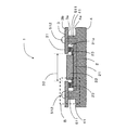
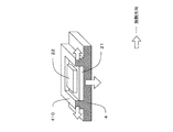
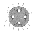
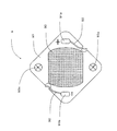
以下、本発明の実施の形態1を、図1〜図3を参照して説明する。図1は、本発明の電気接続装置を用いた光源装置の実施の形態1の構成の概略を示す概略上面図である。図2は、図1におけるA−A線による概略断面図である。図3は、図2における破線領域Bの部分拡大図である。
(Embodiment 1)
Embodiment 1 of the present invention will be described below with reference to FIGS. FIG. 1 is a schematic top view showing an outline of the configuration of the first embodiment of the light source device using the electrical connecting device of the present invention. FIG. 2 is a schematic sectional view taken along line AA in FIG. FIG. 3 is a partially enlarged view of a broken line area B in FIG.

本発明の実施の形態1に係る光源装置1は、発光部22及び電気部品側接続端子である発光モジュール側接続端子を光源基板21の一方の面上に備えた発光モジュール2と、該発光モジュール2に電源を供給するための配線を備えた配線基板3と、前記発光モジュール2を支持し前記配線基板3を取り付ける被取付体である支持部4とを備えている。   The light source device 1 according to the first embodiment of the present invention includes a light emitting module 2 including a light emitting unit 22 and a light emitting module side connection terminal that is an electrical component side connection terminal on one surface of a light source substrate 21, and the light emitting module. 2 includes a wiring board 3 provided with wiring for supplying power to 2, and a support portion 4 that is an attached body that supports the light emitting module 2 and attaches the wiring board 3.

上記構成において、前記発光モジュール2は、光を発する発光部22と、外部からの電源を前記発光部22へと供給するために電気的接続を行う電極パッドからなる発光モジュール側接続端子23と、前記発光部22及び前記発光モジュール側接続端子23を配設するための光源基板21とからなる。   In the above-described configuration, the light emitting module 2 includes a light emitting unit 22 that emits light, and a light emitting module side connection terminal 23 that includes an electrode pad that is electrically connected to supply power from the outside to the light emitting unit 22; It comprises a light source substrate 21 for disposing the light emitting part 22 and the light emitting module side connection terminal 23.

なお、前記発光部22は、前記光源基板21の光源配設面21a上に複数のLED(Light Emitting Diode)ベアチップ(図示せず)を配設した後、該複数のLEDベアチップの上から蛍光体を混合した樹脂性材料にて封止したものである。   The light emitting unit 22 includes a plurality of LEDs (Light Emitting Diode) bare chips (not shown) arranged on the light source arrangement surface 21 a of the light source substrate 21, and then a phosphor from above the plurality of LED bare chips. It is sealed with a resinous material mixed with.

また、光源基板21は放熱性又は熱伝導性の高いアルミナセラミックからなり、略四角形板形状を有し、4つの長辺211と4つの頂点を面取りした短辺212とから構成されている。   The light source substrate 21 is made of alumina ceramic with high heat dissipation or heat conductivity, has a substantially rectangular plate shape, and includes four long sides 211 and short sides 212 having four chamfered chamfers.

そして、前記配線基板3は、前記発光モジュール2の光源配設面21aに対向する光源対向面である配線基板3の下面3aに電極パッドからなる配線基板側接続端子31を備えたプリント基板で、前記配線基板3の下面3aの前記発光モジュール2の発光部22に対向する領域に、前記発光部22と同程度の形状及び大きさを有する孔状の開口である光出射窓32をさらに備えてなるものである。前記光出射窓32を設けることで、光が遮られることなく出射されるため、発光部22からの光を効率的に照明に用いることができる。   The wiring board 3 is a printed board having wiring board side connection terminals 31 formed of electrode pads on the lower surface 3a of the wiring board 3 which is a light source facing surface facing the light source arrangement surface 21a of the light emitting module 2. A light exit window 32 that is a hole-like opening having the same shape and size as the light emitting unit 22 is further provided in a region facing the light emitting unit 22 of the light emitting module 2 on the lower surface 3 a of the wiring board 3. It will be. By providing the light exit window 32, the light is emitted without being blocked, so that the light from the light emitting unit 22 can be used efficiently for illumination.

特に、前記光出射窓32の形状を前記発光モジュール2の発光部22の発光領域と略同一形状及び大きさとなるように設けることで、発光モジュール2の発する光を遮蔽によって減衰させることがなくなり、より効率的に照明に用いることができる。   In particular, by providing the light exit window 32 so that the shape of the light emission window 32 is substantially the same shape and size as the light emitting region of the light emitting unit 22 of the light emitting module 2, light emitted from the light emitting module 2 is not attenuated by shielding, It can be used for illumination more efficiently.

なお、前記配線基板3は、後述する螺合機構を構成する雄ネジを挿通させるためのネジ挿通孔33をさらに設けている。   The wiring board 3 further includes a screw insertion hole 33 for inserting a male screw constituting a screwing mechanism to be described later.

さらに、配線基板3の上面3bの全面には、図1の斜線で示す領域には、熱伝導性の高い銅からなる放熱用パターン34が設けられ、配線基板3や該配線基板3に接する発光モジュール2からの熱を効率的に外部へと逃がす効果がある。   Further, a heat radiation pattern 34 made of copper having high thermal conductivity is provided on the entire surface of the upper surface 3b of the wiring board 3 in the hatched area in FIG. 1 so that the wiring board 3 and the light emission in contact with the wiring board 3 are emitted. There is an effect of efficiently releasing the heat from the module 2 to the outside.

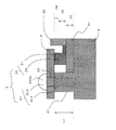
そして、前記支持部4は、光源支持面4aに設けられた2つの支柱41を備える。前記2つの支柱41は四角柱形状を成しており、発光モジュール2の光源基板21の2つの発光モジュール側接続端子23に近い2つの短辺と接するように配設されている。発光モジュール2を配設する際に、前記支柱41をガイド部として配設位置の目安にすることが可能となり、発光モジュール2を配設する作業の効率化を図ることができる。   And the said support part 4 is equipped with the two support | pillar 41 provided in the light source support surface 4a. The two pillars 41 have a quadrangular prism shape, and are disposed so as to be in contact with two short sides close to the two light emitting module side connection terminals 23 of the light source substrate 21 of the light emitting module 2. When the light emitting module 2 is disposed, the support column 41 can be used as a guide for the position of the light emitting module 2, and the efficiency of the work of disposing the light emitting module 2 can be improved.

また、前記支持部4は、銅やアルミ、アルミナセラミック等の放熱性又は熱伝導性の高い素材からなり、前記光源装置の放熱部も兼ねるべく設けられてなるものである。   The support portion 4 is made of a material having high heat dissipation or heat conductivity, such as copper, aluminum, or alumina ceramic. The support portion 4 is also provided to serve as the heat dissipation portion of the light source device.

なお、上述の構成において、前記光源装置1は、前記配線基板3を前記支持部4に取り付けることにより前記配線基板側接続端子31と前記発光モジュール側接続端子23とを接触させて電気的接続を行う接続機構5を有する。該接続機構5は、図3に示す通り、前記発光モジュール2及び前記配線基板3を前記支持部4に取り付けて固定する取付機構である螺合機構51と、前記発光モジュール2の発光モジュール側接続端子23と前記配線基板3の配線基板側接続端子31とを電気的に接続する電気的接続機構52とからなる。   In the above-described configuration, the light source device 1 attaches the wiring board 3 to the support portion 4 to bring the wiring board side connection terminal 31 and the light emitting module side connection terminal 23 into contact with each other for electrical connection. It has a connection mechanism 5 to perform. As shown in FIG. 3, the connection mechanism 5 includes a screwing mechanism 51 that is an attachment mechanism for attaching and fixing the light emitting module 2 and the wiring board 3 to the support portion 4, and the light emitting module 2 side connection of the light emitting module 2. It comprises an electrical connection mechanism 52 that electrically connects the terminal 23 and the wiring board side connection terminal 31 of the wiring board 3.

なお、前記取付機構である螺合機構51は、前記発光モジュール2を前記配線基板3及び前記支持部4にて挟圧して固定する挟圧機構としても機能する。   The screwing mechanism 51 serving as the attachment mechanism also functions as a clamping mechanism that clamps and fixes the light emitting module 2 between the wiring board 3 and the support portion 4.

上述の構成において、前記螺合機構51は、雄ネジと雌ネジの螺合によって前記配線基板3を前記支持部4に取り付けて固定するものであり、該固定された前記配線基板3と前記支持部4との間に配設される前記発光モジュール2を挟圧するものである。   In the above-described configuration, the screwing mechanism 51 attaches and fixes the wiring board 3 to the support portion 4 by screwing a male screw and a female screw, and the fixed wiring board 3 and the support are fixed. The light emitting module 2 disposed between the unit 4 and the unit 4 is clamped.

また、前記電気的接続機構52は、配線基板3の配線基板側接続端子31と発光モジュール2の発光モジュール側接続端子23とからなる。そして、電気的接続機構52は、前記取付機構である挟圧機構としての螺合機構51によって、前記配線基板3と前記支持部4が取り付けられ、また、前記発光モジュール2が前記配線基板3と前記支持部4によって挟圧され、前記発光モジュール2の発光モジュール側接続端子23と前記配線基板3の配線基板側接続端子31の間に前記挟圧する力が働くため、前記発光モジュール2の発光モジュール側接続端子23と前記配線基板3の配線基板側接続端子31とが確実に接触し、電気的接続が確実になされる。   The electrical connection mechanism 52 includes a wiring board side connection terminal 31 of the wiring board 3 and a light emitting module side connection terminal 23 of the light emitting module 2. The electrical connection mechanism 52 is attached to the wiring board 3 and the support portion 4 by a screwing mechanism 51 as a clamping mechanism which is the attachment mechanism, and the light emitting module 2 is connected to the wiring board 3. Since the pressing force acts between the light emitting module side connection terminal 23 of the light emitting module 2 and the wiring board side connection terminal 31 of the wiring board 3, the light emitting module of the light emitting module 2 is clamped by the support portion 4. The side connection terminals 23 and the wiring board side connection terminals 31 of the wiring board 3 are reliably in contact with each other, so that the electrical connection is ensured.

なお、前記螺合機構51についてさらに詳細に説明すると、前記螺合機構51は、雄ネジである固定用ネジ512と前記支柱41の支柱上面41aに設けられた雌ネジであるネジ孔511からなり、固定用ネジ512を前記配線基板3のネジ挿通孔33に挿通させて前記支持部のネジ孔511に螺合させることで前記配線基板3を前記支持部4に取り付けて固定する。ここで、前記固定用ネジ512のヘッド部512aの半径はネジ挿通孔33の半径より大きく設計されており、螺合した際に前記ヘッド部512aが前記配線基板3に密着することで、前記配線基板3は前記支持部4に強固に取り付けられて固定される。   The screwing mechanism 51 will be described in more detail. The screwing mechanism 51 includes a fixing screw 512 that is a male screw and a screw hole 511 that is a female screw provided on the column upper surface 41a of the column 41. Then, the fixing board 512 is inserted into the screw insertion hole 33 of the wiring board 3 and screwed into the screw hole 511 of the support part, thereby attaching and fixing the wiring board 3 to the support part 4. Here, the radius of the head portion 512a of the fixing screw 512 is designed to be larger than the radius of the screw insertion hole 33. When the head portion 512a is brought into close contact with the wiring board 3 when screwed, The substrate 3 is firmly attached and fixed to the support portion 4.

さらに、前記螺合機構51によって前記配線基板3と前記支持部4とが固定される際、前記配線基板3と前記支持部4との間に配設される前記発光モジュール2の発光モジュール側接続端子23と前記配線基板3の配線基板側接続端子31との接触及び電気的接続を確実なものとするため、支柱41の寸法h1は、図3に示す通り、光源基板21の寸法(厚み)h2と発光モジュール側接続端子23の寸法h3と配線基板側接続端子31の寸法h4の総和よりも小さいことが望ましい、即ち、
h1<h2+h3+h4 ・・・・・・・・・・(1)
(1)式を満たすことが望ましい。(1)式を満たす寸法に設定することによって、螺合機構51によって前記配線基板3と前記支持部4が固定された際、前記配線基板3と前記支持部4との間に配設される発光モジュール2が挟圧され、該発光モジュール2の発光モジュール側接続端子23と前記配線基板3の配線基板側接続端子31との間に挟圧のための力が働いて、前記発光モジュール側接続端子23と前記配線基板側接続端子31は、確実に、機械的かつ電気的に接続されることとなる。
Further, when the wiring board 3 and the support part 4 are fixed by the screwing mechanism 51, the light emitting module side connection of the light emitting module 2 disposed between the wiring board 3 and the support part 4. In order to ensure contact and electrical connection between the terminal 23 and the wiring board side connection terminal 31 of the wiring board 3, the dimension h1 of the column 41 is the dimension (thickness) of the light source board 21 as shown in FIG. It is desirable that it is smaller than the sum total of h2 and the dimension h3 of the light emitting module side connection terminal 23 and the dimension h4 of the wiring board side connection terminal 31.
h1 <h2 + h3 + h4 (1)
It is desirable to satisfy the equation (1). By setting the dimensions to satisfy the formula (1), when the wiring board 3 and the support part 4 are fixed by the screwing mechanism 51, the dimensions are arranged between the wiring board 3 and the support part 4. The light emitting module 2 is clamped, and a force for clamping acts between the light emitting module side connection terminal 23 of the light emitting module 2 and the wiring board side connection terminal 31 of the wiring board 3, so that the light emitting module side connection is performed. The terminal 23 and the wiring board side connection terminal 31 are reliably mechanically and electrically connected.

上述のように、前記発光モジュール2は、前記支持部4へ取り付けるための機構を前記発光モジュール2自体の構成としては備えておらず、前記配線基板3が前記支持部4に取り付けられる際に、前記発光モジュール2が前記配線基板3と前記支持部4との間に予め配設されていることで、前記配線基板3が前記支持部4に取り付けられると同時に、前記配線基板3と前記支持部4に挟圧されるという形での取り付けがなされる構成である。本明細書中では、このような構成要素自体には取り付けるための機構を有さず、他の構成要素の取り付けの関係で取り付けられることを「間接的に取り付けられる」と表現する。   As described above, the light emitting module 2 does not include a mechanism for attaching to the support portion 4 as a configuration of the light emitting module 2 itself, and when the wiring board 3 is attached to the support portion 4, Since the light emitting module 2 is disposed between the wiring board 3 and the support part 4 in advance, the wiring board 3 is attached to the support part 4 and at the same time, the wiring board 3 and the support part. In this configuration, attachment is performed in such a manner as to be clamped between the four. In the present specification, such a component itself does not have a mechanism for attachment, and that it is attached in relation to attachment of other components is expressed as “indirectly attached”.

また、本実施の形態1において、光源装置1は、1つの前記発光モジュール2に対して複数箇所に電気的接続機構を設けているため、各電気的接続機構において、発光モジュール側接続端子23の寸法h3や配線基板側接続端子31の寸法h4などにばらつきが生じる場合がある。しかし、各電気的接続機構を設けた箇所の付近に螺合機構が設けられているため、各電気的接続機構を設けた箇所において、h1〜h4の寸法に合わせて前記螺合機構51を用いて挟圧する力を調節することで、前記発光モジュール2の発光モジュール側接続端子23と前記配線基板3の配線基板側接続端子31との強固な接触を実現し、確実な電気的接続が可能となる。   In the first embodiment, the light source device 1 is provided with electrical connection mechanisms at a plurality of locations with respect to one light-emitting module 2. Therefore, in each electrical connection mechanism, the light-emitting module side connection terminal 23 is connected. Variations may occur in the dimension h3, the dimension h4 of the wiring board side connection terminal 31, and the like. However, since the screwing mechanism is provided in the vicinity of the location where each electrical connection mechanism is provided, the screwing mechanism 51 is used in accordance with the dimensions of h1 to h4 at the location where each electrical connection mechanism is provided. By adjusting the clamping force, a firm contact between the light emitting module side connection terminal 23 of the light emitting module 2 and the wiring board side connection terminal 31 of the wiring board 3 can be realized, and a reliable electrical connection can be achieved. Become.

例えば、前記発光モジュール2の発光モジュール側接続端子23と前記配線基板3の配線基板側接続端子31との接触が弱く、電気的接続が確実ではない箇所があれば、その最も近くにある螺合機構51の螺合を強固にすることで、該螺合機構51付近での前記発光モジュール2を挟圧する力が大きくなり、部分的に挟圧する力が強くなることで配線基板3が撓んで、前記発光モジュール2の発光モジュール側接続端子23と前記配線基板3の配線基板側接続端子31との接触をより強固にすることが可能となる。   For example, if there is a place where the contact between the light emitting module side connection terminal 23 of the light emitting module 2 and the wiring board side connection terminal 31 of the wiring board 3 is weak and electrical connection is not reliable, the nearest screwing is performed. By strengthening the screwing of the mechanism 51, the force for pinching the light emitting module 2 in the vicinity of the screwing mechanism 51 is increased, and the force for partially pinching is increased, whereby the wiring board 3 is bent, The contact between the light emitting module side connection terminal 23 of the light emitting module 2 and the wiring board side connection terminal 31 of the wiring board 3 can be further strengthened.

上述の通り、発光モジュール2と配線基板3を被取付体である支持部4に取り付けることにより、前記発光モジュール2と前記配線基板3とが接触して電気的接続が為されるため、前記発光モジュール2と前記配線基板3を取り付けた後に別途電気的接続を行う作業工程が不要となり、全体の組立作業工程数が少なくなる。   As described above, since the light emitting module 2 and the wiring board 3 are attached to the support portion 4 that is an attachment body, the light emitting module 2 and the wiring board 3 are brought into contact with each other to be electrically connected. After the module 2 and the wiring board 3 are attached, a separate work process for electrical connection becomes unnecessary, and the total number of assembly work processes is reduced.

なお、本発明の光源装置は、照明装置を構成する光源として用いても良いし、表示装置を構成する光源として用いても良いし、その他様々な装置を構成する光源として用いて良い。   The light source device of the present invention may be used as a light source that constitutes an illumination device, may be used as a light source that constitutes a display device, or may be used as a light source that constitutes various other devices.

また、本発明の実施の形態1において、光源装置1の支持部4に設けられたガイド部としての支柱41の形状は、四角柱形状を成しており、発光モジュール2の光源基板21の2つの発光モジュール側接続端子23に近い2つの短辺と接するように配設されているものとしたが、これに限られることはなく、支柱41の形状及び大きさは、図4に示す支柱壁410のように、光源基板21の外形に沿った形状及び大きさとしても良い。前記支柱壁410が発光モジュール2の光源基板21の四方の側面に熱接触することで、放熱部でもある支持部4との接触面積が増加し放熱性能の向上が図れる。なお、本明細書において前記熱接触というのは、熱伝導が十分に行われる程度の接触を指し、必ずしも接触する面の全体が接している必要はない。   Moreover, in Embodiment 1 of this invention, the shape of the support | pillar 41 as a guide part provided in the support part 4 of the light source device 1 has comprised square pillar shape, and 2 of the light source substrate 21 of the light emitting module 2 is used. The two light emitting module side connection terminals 23 are disposed so as to be in contact with the two short sides, but the present invention is not limited to this, and the shape and size of the support column 41 are shown in FIG. As in 410, the shape and size of the light source substrate 21 may be taken along the outer shape. Since the support wall 410 is in thermal contact with the four side surfaces of the light source substrate 21 of the light emitting module 2, the contact area with the support portion 4 that is also a heat dissipation portion is increased, and the heat dissipation performance can be improved. In addition, in this specification, the said heat contact refers to the contact of the grade which heat conduction is fully performed, and the whole surface to contact does not necessarily need to be in contact.

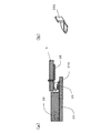
さらに、本発明の実施の形態1において、光源装置1の配線基板3の配線基板側接続端子31は、電極パッド同士の接触であるとしたが、これに限られることはなく、図5(a),(b)に示す配線側バネ接続端子310のように、湾曲した板バネを用いたバネ構造を有していても良い。挟圧構造にて挟圧されることにより配線側バネ接続端子310が撓み、挟圧される以前の形状へ復元しようとする復元力がかかることにより、確実に接触が為され、電極パッド同士の接触に比べて信頼性の高い確実な電気的接続が可能となる。   Furthermore, in Embodiment 1 of this invention, although the wiring board side connection terminal 31 of the wiring board 3 of the light source device 1 was contact between electrode pads, it is not restricted to this, FIG. And a spring structure using a curved leaf spring, such as the wiring-side spring connection terminal 310 shown in FIGS. By being pinched by the pinching structure, the wiring side spring connection terminal 310 is bent and a restoring force is applied to restore the shape before being pinched, so that contact is reliably made and the electrode pads Reliable and reliable electrical connection is possible compared to contact.

また、図5(a),(b)に示す配線側バネ接続端子310を用いると、特に複数点で発光モジュール2と配線基板3が接触する場合に効果的である。つまり、接続端子の大きさや発光モジュール2の光源基板21及び配線基板3の厚みのバラツキが生じる可能性があるのだが、各配線側バネ接続端子310が可撓性を有しているため、それぞれの端子間距離に応じて撓むことで、端子間距離のバラツキが生じていても、配線基板側接続端子310と発光モジュール側接続端子23の間で電気的接続が実現される。   5A and 5B is effective particularly when the light emitting module 2 and the wiring board 3 are in contact with each other at a plurality of points. That is, there is a possibility that the size of the connection terminal and the thickness of the light source board 21 and the wiring board 3 of the light emitting module 2 may vary, but each wiring-side spring connection terminal 310 has flexibility, By bending according to the inter-terminal distance, electrical connection is realized between the wiring board side connection terminal 310 and the light emitting module side connection terminal 23 even if the inter-terminal distance varies.

なお、バネ構造は板バネ以外にも、コイルバネ(スプリング)を利用した押バネや引っ張りバネを利用しても良い。また、バネ構造は配線基板3の配線基板側接続端子310側ではなく、発光モジュール2の発光モジュール側接続端子23側に設けても良いし、配線基板側接続端子310及び発光モジュール側接続端子23の両方にバネ構造の接続端子を設けても良い。   The spring structure may use a push spring or a tension spring using a coil spring (spring) in addition to the plate spring. The spring structure may be provided not on the wiring board side connection terminal 310 side of the wiring board 3 but on the light emitting module side connection terminal 23 side of the light emitting module 2, or on the wiring board side connection terminal 310 and the light emitting module side connection terminal 23. Both of them may be provided with connection terminals having a spring structure.

そして、本発明の実施の形態1において、光源装置1は、雄ネジである固定用ネジ512及び被取付体である支持部4に備えたネジ孔511との螺合機構51にて、前記配線基板3が前記支持部4に取り付けられる際に、前記配線基板3と前記支持部4との間に配設されている前記発光モジュール2が間接的に取り付けられる構成としたが、これに限られることはなく、例えば、前記発光モジュール2にネジ孔を設け、該ネジ孔と前記配線基板3のネジ挿通孔33を挿通する固定用ネジ512との螺合機構によって、前記発光モジュール2と前記配線基板3とを取り付けても良い。本明細書において、このように、構成要素自体に取り付けるための機構の一部を有しており、他の構成要素に取り付けられることを「直接的に取り付けられる」と表現する。   In Embodiment 1 of the present invention, the light source device 1 uses the screwing mechanism 51 with the fixing screw 512 that is a male screw and the screw hole 511 provided in the support portion 4 that is the attached body. When the substrate 3 is attached to the support portion 4, the light emitting module 2 disposed between the wiring substrate 3 and the support portion 4 is indirectly attached. For example, the light emitting module 2 and the wiring are provided by a screwing mechanism between the screw hole and the fixing screw 512 through which the screw hole is inserted into the screw insertion hole 33 of the wiring board 3. A substrate 3 may be attached. In this specification, it has a part of the mechanism for attaching to the component itself as described above, and attaching to another component is expressed as “directly attached”.

また、本発明の実施の形態1において、配線基板3の放熱用パターン34は、銅のパターンを用いて説明したが、これに限られることはなく、他の熱伝導性の高い金属を用いても良いし、凹凸形状などの形状パターンで表面積を大きくして放熱用パターンとしても良いし、金属パターンと形状パターンの両方を用いても良い。   In Embodiment 1 of the present invention, the heat radiation pattern 34 of the wiring board 3 has been described using a copper pattern. However, the present invention is not limited to this, and another metal having high thermal conductivity is used. Alternatively, the heat radiation pattern may be obtained by increasing the surface area with a shape pattern such as a concavo-convex shape, or both a metal pattern and a shape pattern may be used.

さらに、本発明の実施の形態1において、光出射窓32は孔状の開口として説明したが、これに限られるものではなく、透明な樹脂板を用いて発光モジュール2からの光を透過して出射しても良いし、半透明な樹脂板を用いても良い。樹脂板を用いることで、埃塵などのゴミが発光モジュール2付近に溜まることを防ぐことができる。   Furthermore, in Embodiment 1 of this invention, although the light emission window 32 demonstrated as a hole-shaped opening, it is not restricted to this, The light from the light emitting module 2 is permeate | transmitted using a transparent resin board. The light may be emitted or a translucent resin plate may be used. By using the resin plate, dust such as dust can be prevented from collecting near the light emitting module 2.

そして、本発明の実施の形態1において、発光モジュール2は、光源基板21の光源配設面21a上に複数のLEDベアチップを配設した後に蛍光体を混合した樹脂性材料にて封止したものとして説明したが、これに限られるものではなく、有機ELなどの他の光源を用いても良い。   In the first embodiment of the present invention, the light emitting module 2 is sealed with a resin material mixed with phosphors after a plurality of LED bare chips are arranged on the light source arrangement surface 21a of the light source substrate 21. However, the present invention is not limited to this, and other light sources such as an organic EL may be used.

さらにまた、本発明の実施の形態1において、挟圧機構としての螺合機構51は、雄ネジと雌ネジの螺合によって前記配線基板3と前記支持部4を固定する螺合機構51を複数備えるものとして説明したが、これに限られるものではなく、支持部4が配線基板3を嵌合する嵌合機構を備え、該嵌合機構によって前記配線基板3と前記支持部4が固定されることで、間に挟まれる前記発光モジュール2と前記配線基板3との電気的接続が為されるとしても良い。   Furthermore, in the first embodiment of the present invention, the screwing mechanism 51 as the clamping mechanism includes a plurality of screwing mechanisms 51 that fix the wiring board 3 and the support portion 4 by screwing a male screw and a female screw. Although described as what is provided, it is not restricted to this, The support part 4 is provided with the fitting mechanism which fits the wiring board 3, and the said wiring board 3 and the said support part 4 are fixed by this fitting mechanism. Thus, electrical connection between the light emitting module 2 and the wiring board 3 sandwiched therebetween may be performed.

(実施の形態2)
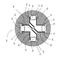
次に、本発明の光源装置の実施の形態2について、図6〜図8を用いて説明する。なお、上記実施の形態1と同一部分には同一符号を付し、その説明は省略する。図6は本発明の光源装置の実施の形態2の構成の概略を示す概略上面図である。図7は図6の配線基板30の概略上面図である。図8は図6の配線基板30の概略下面図である。
(Embodiment 2)
Next, a second embodiment of the light source device of the present invention will be described with reference to FIGS. The same parts as those in the first embodiment are denoted by the same reference numerals, and the description thereof is omitted. FIG. 6 is a schematic top view showing an outline of the configuration of the light source device according to Embodiment 2 of the present invention. FIG. 7 is a schematic top view of the wiring board 30 of FIG. FIG. 8 is a schematic bottom view of the wiring board 30 of FIG.

本発明の光源装置1Aは、実施の形態1と同様に、発光部22及び発光モジュール側接続端子23を光源基板の一方の面上に備えた発光モジュール2と、前記発光モジュール2を支持し前記配線基板3を取り付ける被取付体である支持部4とを設けて構成するものである。   As in Embodiment 1, the light source device 1A according to the present invention supports the light emitting module 2 including the light emitting unit 22 and the light emitting module side connection terminal 23 on one surface of the light source substrate, and supports the light emitting module 2. A support portion 4 which is an attached body to which the wiring board 3 is attached is provided and configured.

なお、本発明の実施の形態2の光源装置1Aにおいては、発光モジュール2を4個配設し、該4個の発光モジュール2の発光部22に対応する位置に光出射窓32を有する配線基板30を備えた構成となっている。   In the light source device 1A according to Embodiment 2 of the present invention, four light emitting modules 2 are arranged, and a wiring board having a light exit window 32 at a position corresponding to the light emitting portions 22 of the four light emitting modules 2. 30 is provided.

ここで、配線基板30について詳細に説明する。配線基板30は円形板上のプリント基板からなり、上面から見ると、図7に示すように、4個の光出射窓32が同一半径の円周上に等間隔で配設され、各光出射窓32付近には、螺合機構51を構成する雄ネジである固定用ネジ512を通すためのネジ挿通孔33が2箇所、配線基板30に対して合計8箇所に設けられている。同一半径の円周上に等間隔で配設することで、各発光モジュール2間の距離が一定に保たれ、発光モジュール2から発生する熱が等間隔で支持部4に伝わるため、熱の偏りが生じたり、急激な温度勾配になる可能性を低減したりすることが可能となり、効率の良い放熱効果が得られる。   Here, the wiring board 30 will be described in detail. The wiring board 30 is composed of a printed board on a circular plate. When viewed from above, as shown in FIG. 7, four light emission windows 32 are arranged on the circumference of the same radius at equal intervals, and each light emission In the vicinity of the window 32, two screw insertion holes 33 for passing fixing screws 512 that are male screws constituting the screwing mechanism 51 are provided at eight places in total with respect to the wiring board 30. By disposing the light emitting modules 2 at equal intervals on the circumference of the same radius, the distance between the light emitting modules 2 is kept constant, and the heat generated from the light emitting modules 2 is transmitted to the support portion 4 at equal intervals. Or the possibility of a steep temperature gradient can be reduced, and an efficient heat dissipation effect can be obtained.

また、配線基板30の上面には、熱伝導性の高い銅からなる放熱用パターン34が設けられ、配線基板30や該配線基板30に接する発光モジュール2からの熱を効率的に外部へと逃がす効果がある。   In addition, a heat radiation pattern 34 made of copper having high thermal conductivity is provided on the upper surface of the wiring board 30, and the heat from the wiring board 30 and the light emitting module 2 in contact with the wiring board 30 is efficiently released to the outside. effective.

さらに、配線基板30の下面には、図8に示すように、配線用パターン35が設けられている。配線用パターン35は、配線基板3の下面中央にあるコネクタ36から2個の発光モジュール2を直列接続すべく、銅線にてパターニングされている。前記発光モジュール2を2個ずつ直列接続することで、光源装置1Aの2系統制御が可能となり、系統別に点灯を制御したり、どちらか一方の系統において断線等の故障が生じた場合でも照明を継続するよう制御したりすることが可能となる。   Furthermore, a wiring pattern 35 is provided on the lower surface of the wiring board 30 as shown in FIG. The wiring pattern 35 is patterned with a copper wire so as to connect the two light emitting modules 2 in series from the connector 36 at the center of the lower surface of the wiring board 3. By connecting the two light emitting modules 2 in series, two systems of the light source device 1A can be controlled, and lighting can be controlled for each system or even when a failure such as a disconnection occurs in either system. It can be controlled to continue.

そして、前記放熱用パターン34は前記配線基板30の下面にも存在し、前記コネクトから4個の発光モジュールへと電気的接続を行っている配線用パターン35を避けるべく設けられている。   The heat radiation pattern 34 also exists on the lower surface of the wiring board 30 and is provided to avoid the wiring pattern 35 that is electrically connected from the connect to the four light emitting modules.

なお、本実施の形態2において、前記発光モジュール2を2個ずつ直列接続することで、光源装置1Aの2系統制御を行うものとして説明したが、これに限られることはなく、1個の発光モジュールからなる系統と3個の発光モジュールからなる系統の夫々を制御する2系統制御でも良いし、2系統制御だけでなく、3系統もしくは4系統で発光モジュールの点灯・消灯・調光を制御する仕様としても良く、多様な制御を行うことが可能である。   In the second embodiment, it has been described that the two light emitting modules 2 are connected in series to perform two-system control of the light source device 1A. However, the present invention is not limited to this, and one light emission is performed. Two-system control that controls each of the system composed of modules and the system composed of three light-emitting modules may be used, and not only the two-system control but also the three-system or four-system control the lighting / extinction / dimming of the light-emitting modules. The specification is good, and various controls can be performed.

また、前記発光モジュール2及び前記配線基板30の光出射窓32は、同一半径の円周上に等間隔で4個ずつ配設したが、これに限られることはなく、複数半径の円周上の各円周上に複数個ずつ等間隔で配設しても良いし、多角形環上に複数個ずつ等間隔で配置しても良い。   Further, four light emitting windows 32 of the light emitting module 2 and the wiring board 30 are arranged at equal intervals on the circumference of the same radius, but the present invention is not limited to this. A plurality of them may be arranged at equal intervals on each circumference of the circle, or a plurality of them may be arranged at equal intervals on the polygonal ring.

(実施の形態3)
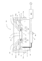
次に、本発明の光源装置の実施の形態3について、図9及び図10を用いて説明する。なお、上記実施の形態1及び実施の形態2と同一部分には同一符号を付し、その説明は省略する。図9は、本発明の光源装置の実施の形態3の構成の概略を示す概略斜視図である。図10は、図9におけるC−C線による概略断面図である。
(Embodiment 3)
Next, a third embodiment of the light source device of the present invention will be described with reference to FIGS. In addition, the same code | symbol is attached | subjected to the same part as the said Embodiment 1 and Embodiment 2, and the description is abbreviate | omitted. FIG. 9 is a schematic perspective view showing an outline of the configuration of Embodiment 3 of the light source device of the present invention. 10 is a schematic cross-sectional view taken along line CC in FIG.

本発明の光源装置1Bは、本発明の実施の形態1と同様に、発光部22及び発光モジュール側接続端子23を光源基板の一方の面上に備えた発光モジュール2と、該発光モジュール2に電源を供給するための配線を備えた配線基板3と、前記発光モジュール2を支持し前記配線基板3を取り付ける被取付体である支持部4とを設けて構成するものである。   As in the first embodiment of the present invention, the light source device 1B of the present invention includes a light emitting module 2 having a light emitting unit 22 and a light emitting module side connection terminal 23 on one surface of the light source substrate, and the light emitting module 2 includes The wiring board 3 is provided with wiring for supplying power, and a support portion 4 that supports the light emitting module 2 and is attached to which the wiring board 3 is attached.

また、光源装置1Bは、光学部材として反射板61と透過板62を、外装体として器具ケース71をさらに備える。また、前記支持部4も外装体の一部を兼ねる。   The light source device 1B further includes a reflection plate 61 and a transmission plate 62 as optical members, and an instrument case 71 as an exterior body. Moreover, the said support part 4 also serves as a part of exterior body.

なお、前記器具ケース71は、器具ケース固定用ネジ71aにて前記支持部4に固定される。   The instrument case 71 is fixed to the support portion 4 with an instrument case fixing screw 71a.

次に電力の供給方法について説明する。外部から供給される商用交流電源を電源ユニット80にて定電流に変換し、変換された定電流が外装体底部である支持部4底面に設けた端子台8に供給され、該端子台8から支持部4を貫通する孔を通るワイヤーハーネス81が配線基板3に設けられたコネクタ36と接続され、配線基板3の配線用パターンを通り、配線基板側接続端子31から発光モジュール2の発光モジュール側接続端子23を通って供給される。   Next, a method for supplying power will be described. The commercial AC power supplied from the outside is converted into a constant current by the power supply unit 80, and the converted constant current is supplied to the terminal block 8 provided on the bottom surface of the support portion 4 that is the bottom of the exterior body. A wire harness 81 that passes through a hole penetrating the support portion 4 is connected to a connector 36 provided on the wiring board 3, passes through a wiring pattern on the wiring board 3, and is connected to the light emitting module 2 side of the light emitting module 2 from the wiring board side connection terminal 31. It is supplied through the connection terminal 23.

なお、前記端子台8は、該端子台8を固定する端子台固定用ネジ8aによって固定されている。   The terminal block 8 is fixed by terminal block fixing screws 8 a for fixing the terminal block 8.

また、本発明の実施の形態3では、前記発光モジュール2は1つしか配設されなかったが、コレに限られるものではなく、例えば、本発明の実施の形態2で説明したように、複数個の発光モジュール2を配設し、該各発光モジュール2からの光を透過すべく、該各発光モジュール2の発光部22に対応した領域に光出射窓32とを有する配線基板30を用いても良い。   In the third embodiment of the present invention, only one light emitting module 2 is provided, but the present invention is not limited to this, and for example, as described in the second embodiment of the present invention, a plurality of light emitting modules 2 are provided. A wiring board 30 having a light emitting window 32 in a region corresponding to the light emitting portion 22 of each light emitting module 2 is used to dispose the light emitting modules 2 and transmit light from each light emitting module 2. Also good.

(実施の形態4)
次に、本発明の光源装置の実施の形態4について、本発明の実施の形態1と同様に、図11を用いて説明する。なお、上記実施の形態1〜実施の形態3と同一部分には同一符号を付し、その説明は省略する。図11は、本発明の光源装置の実施の形態4の構成の概略を示す概略断面図である。
(Embodiment 4)
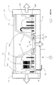
Next, the fourth embodiment of the light source device of the present invention will be described using FIG. 11 as in the first embodiment of the present invention. In addition, the same code | symbol is attached | subjected to the same part as the said Embodiment 1-Embodiment 3, and the description is abbreviate | omitted. FIG. 11: is a schematic sectional drawing which shows the outline of a structure of Embodiment 4 of the light source device of this invention.

本発明の光源装置1Cは、実施の形態3と同様に、発光部22及び発光モジュール側接続端子23を光源基板21の一方の面上に備えた発光モジュール2と、該発光モジュール2に電源を供給するための配線を備えた配線基板300と、前記発光モジュール2を支持し前記配線基板300を取り付ける被取付体である支持部4と、光学部材として反射板61と透過板62を、外装体として器具ケース71をさらに備える。なお、前記支持部4及び前記透過板62も外装体の一部を兼ねる。   In the light source device 1C of the present invention, as in the third embodiment, the light emitting module 2 provided with the light emitting unit 22 and the light emitting module side connection terminal 23 on one surface of the light source substrate 21, and the light emitting module 2 is powered. A wiring board 300 having wirings to be supplied, a support portion 4 that is an attached body that supports the light emitting module 2 and attaches the wiring board 300, a reflection plate 61 and a transmission plate 62 as optical members, and an exterior body An instrument case 71 is further provided. The support 4 and the transmission plate 62 also serve as a part of the exterior body.

また、前記配線基板300は、該配線基板300上に設けられた発光モジュール2を駆動すべく、外部からの供給された電源を定電流に変換して供給する定電流電源回路を内蔵した回路部37を有するものである。   Further, the wiring board 300 has a built-in constant current power supply circuit that converts an externally supplied power into a constant current to drive the light emitting module 2 provided on the wiring board 300. 37.

上記の構成において、前記回路部37は、抵抗37aやコンデンサ37b、コイル37c、FET37dなどの回路部品からなる。   In the above configuration, the circuit unit 37 includes circuit components such as a resistor 37a, a capacitor 37b, a coil 37c, and an FET 37d.

なお、前記FET37dのように発熱量の大きな回路部品は、外装体である器具ケース71付近に配設することが望ましい。発熱量の大きな回路部品を外装体付近に配設することで、回路部品から発せられる熱が外装体である器具ケース71に早期に伝わり、光源装置内部に熱が溜まることを防止することができる。このように、外装体である器具ケース71は、外装体の一部を兼ねる前記支持部4とともに、前記発光モジュール2及び発熱する回路部品の熱を外部へ放出するための放熱部として機能している。   It should be noted that a circuit component having a large calorific value, such as the FET 37d, is preferably disposed in the vicinity of the instrument case 71 which is an exterior body. By disposing a circuit component having a large calorific value in the vicinity of the exterior body, it is possible to prevent heat generated from the circuit component from being transmitted to the instrument case 71 that is the exterior body at an early stage and to accumulate heat inside the light source device. . Thus, the instrument case 71 which is an exterior body functions as a heat radiating section for releasing heat of the light emitting module 2 and the heat generating circuit component to the outside together with the support section 4 also serving as a part of the exterior body. Yes.

また、前記発光モジュール2は前記FET37dと同じく発熱量の大きな回路部品であるため、発熱量の大きな複数の回路部品の間隔や、該発熱量の大きな回路部品と発光モジュール2との間隔は、駆動中の配線基板300又は光源装置1C全体の温度勾配が緩やかになるよう、互いに離れて配置することが望ましい。駆動中の配線基板300又は光源装置1C全体の温度勾配が緩やかになることで、回路部品や発光モジュール2からの熱が局所的に溜まり高温に達し、回路部品や発光モジュール2などを損傷することを防ぐことができる。   Further, since the light emitting module 2 is a circuit component having a large calorific value like the FET 37d, the interval between a plurality of circuit components having a large calorific value and the interval between the circuit component having a large calorific value and the light emitting module 2 are driven. It is desirable to arrange them apart from each other so that the temperature gradient of the entire wiring board 300 or the entire light source device 1C becomes gentle. When the temperature gradient of the driving wiring board 300 or the entire light source device 1C becomes gentle, heat from the circuit components and the light emitting module 2 is locally accumulated and reaches a high temperature, and the circuit components and the light emitting module 2 are damaged. Can be prevented.

さらに、前記器具ケース71が熱伝導性の高い金属やセラミック等の素材からなり、放熱性を有している場合は、発熱量の大きな回路部品は前記器具ケース71に熱接触すべく前記配線基板300に備えられると良い。前記器具ケース71が放熱性を有し、発熱量の大きな回路部品と熱的に接触していることで、前記回路部品の熱が速やかに前記器具ケース71へと伝わり、該器具ケース71に伝わった熱は外部へと放出されるため、効率的な放熱が可能となる。   Further, when the instrument case 71 is made of a material such as a metal or ceramic having high thermal conductivity and has a heat dissipation property, a circuit component having a large amount of generated heat is required to be in thermal contact with the instrument case 71. 300 may be provided. Since the instrument case 71 has heat dissipation and is in thermal contact with a circuit component that generates a large amount of heat, the heat of the circuit component is quickly transmitted to the instrument case 71 and is transmitted to the instrument case 71. Since the generated heat is released to the outside, efficient heat dissipation is possible.

上述した通り、発光モジュール2を駆動するための定電流を供給する定電流電源回路を備えた回路部品37を光源装置1C内部に設けることで、商用交流電源を定電流に変換するための電源ユニットを別途設ける必要がなくなり、装置全体としての導入コストを低減でき、また、光源装置施工時の作業負担も低減できる。   As described above, a power supply unit for converting a commercial AC power source into a constant current by providing a circuit component 37 having a constant current power source circuit for supplying a constant current for driving the light emitting module 2 inside the light source device 1C. It is not necessary to provide a separate light source, so that the introduction cost of the entire apparatus can be reduced, and the work burden when constructing the light source device can be reduced.

さらに、実施の形態2で説明した、発光モジュール2を複数個設けた場合の配線基板30を有しても良い。   Furthermore, you may have the wiring board 30 at the time of providing the light emitting module 2 demonstrated in Embodiment 2 in multiple numbers.

本発明の電気接続装置を用いた光源装置の実施の形態1の構成の概略を示す概略上面図である。It is a schematic top view which shows the outline of a structure of Embodiment 1 of the light source device using the electrical connection apparatus of this invention. 図1におけるA−A線による概略断面図である。It is a schematic sectional drawing by the AA in FIG. 図2における破線領域Bの部分拡大図である。It is the elements on larger scale of the broken-line area | region B in FIG. 本発明の支持部に備えられたガイド部の他の例を示す概略斜視図である。It is a schematic perspective view which shows the other example of the guide part with which the support part of this invention was equipped. (a)本発明の配線基板側接続端子の他の例を示す概略斜視図である。(b)本発明の配線基板側接続端子の要部拡大図である。(A) It is a schematic perspective view which shows the other example of the wiring board side connection terminal of this invention. (B) It is a principal part enlarged view of the wiring board side connection terminal of this invention. 本発明の光源装置の実施の形態2の構成の概略を示す概略上面図である。It is a schematic top view which shows the outline of a structure of Embodiment 2 of the light source device of this invention. 図6の配線基板の概略上面図である。It is a schematic top view of the wiring board of FIG. 図8は図6の配線基板の概略下面図である。FIG. 8 is a schematic bottom view of the wiring board of FIG. 本発明の光源装置の実施の形態3の構成の概略を示す概略斜視図である。It is a schematic perspective view which shows the outline of a structure of Embodiment 3 of the light source device of this invention. 図9におけるC−C線による概略断面図である。It is a schematic sectional drawing by CC line in FIG. 本発明の光源装置の実施の形態4の構成の概略を示す概略断面図である。It is a schematic sectional drawing which shows the outline of a structure of Embodiment 4 of the light source device of this invention. 従来の光源装置の構成を示す概略上面図である。It is a schematic top view which shows the structure of the conventional light source device.

符号の説明Explanation of symbols

1,1A,1B,1C 光源装置
2,9 発光モジュール
3,30,300 配線基板
4 支持部
4a 光源支持面
5 接続機構
8 端子台
21,93 光源基板
21a 光源配設面
22,90 発光部
23 発光モジュール側接続端子
31,310 配線基板側接続端子
32 光出射窓
33 ネジ挿通孔
34 放熱用パターン
35 配線用パターン
36 コネクタ
37 回路部
41 支柱
51 螺合機構
52 電気的接続機構
61 反射板
62 透過板
71 器具ケース
410 支柱壁
511 ネジ孔
512 固定用ネジ
1, 1A, 1B, 1C Light source device 2, 9 Light emitting module 3, 30, 300 Wiring board 4 Support part 4a Light source support surface 5 Connection mechanism 8 Terminal block 21, 93 Light source board 21a Light source arrangement surface 22, 90 Light emission part 23 Light emitting module side connection terminals 31, 310 Wiring board side connection terminals 32 Light exit window 33 Screw insertion hole 34 Heat radiation pattern 35 Wiring pattern 36 Connector 37 Circuit part 41 Support column 51 Screwing mechanism 52 Electrical connection mechanism 61 Reflecting plate 62 Transmission Plate 71 Instrument case 410 Column wall 511 Screw hole 512 Fixing screw

Claims (13)

発光モジュール等の電気部品と、配線基板と、前記電気部品及び前記配線基板を取り付ける被取付体とからなる電気接続装置であって、
前記配線基板を前記被取付体に取り付けることにより、前記電気部品と前記配線基板の電気的接続を行う接続機構を有することを特徴とする電気接続装置。
An electrical connection device comprising an electrical component such as a light emitting module, a wiring board, and an attachment body to which the electrical component and the wiring board are attached,
An electrical connection apparatus comprising: a connection mechanism for electrically connecting the electrical component and the wiring board by attaching the wiring board to the attached body.
前記接続機構は、前記配線基板を前記被取付体に取り付ける取付機構と、前記電気部品の電気部品側接続端子と前記配線基板の配線基板側接続端子とを電気的に接続する電気的接続機構とからなることを特徴とする請求項1に記載の電気接続装置。   The connection mechanism includes an attachment mechanism for attaching the wiring board to the attached body, an electrical connection mechanism for electrically connecting an electrical component side connection terminal of the electrical component and a wiring board side connection terminal of the wiring board, and The electrical connection device according to claim 1, comprising: 前記電気部品は、前記配線基板と前記被取付体との間に配設され、
前記取付機構は、前記電気部品を挟圧すべく前記配線基板と前記被取付体とを取り付ける挟圧機構を有することを特徴とする請求項2に記載の電気接続装置。
The electrical component is disposed between the wiring board and the attached body,
The electrical connection device according to claim 2, wherein the attachment mechanism includes a clamping mechanism that attaches the wiring board and the attached body so as to clamp the electrical component.
前記挟圧機構として、1つの前記電気部品に対して複数の螺合機構を備えることを特徴とする請求項3に記載の電気接続装置。   The electrical connecting device according to claim 3, wherein the clamping mechanism includes a plurality of screwing mechanisms for one electrical component. 前記螺合機構は、前記電気部品側接続端子及び前記配線基板側接続端子付近にて螺合することを特徴とする請求項4に記載の電気接続装置。   The electrical connection device according to claim 4, wherein the screwing mechanism is screwed in the vicinity of the electrical component side connection terminal and the wiring board side connection terminal. 前記電気部品側接続端子及び前記配線基板側接続端子の少なくともどちらか一方は、バネ構造の接続端子であることを特徴とする請求項2から請求項5のいずれか1つに記載の電気接続装置。   The electrical connection device according to any one of claims 2 to 5, wherein at least one of the electrical component side connection terminal and the wiring board side connection terminal is a connection terminal having a spring structure. . 前記被取付体は、前記電気部品を取り付けるためのガイド部を有することを特徴とする請求項1から請求項6のいずれか1つに記載の電気接続装置。   The electrical connection apparatus according to claim 1, wherein the attached body includes a guide portion for mounting the electrical component. 請求項1から7のいずれか1つに記載の電気接続装置を備える光源装置であって、
前記電気部品は、一方の面に発光部を備えた発光モジュールであることを特徴とする光源装置。
A light source device comprising the electrical connection device according to any one of claims 1 to 7,
The light source device, wherein the electrical component is a light emitting module having a light emitting portion on one surface.
前記接続機構は、前記発光部を備えた一方の面側から前記配線基板を取り付けることを特徴とする請求項8に記載の光源装置。   The light source device according to claim 8, wherein the connection mechanism attaches the wiring board from one surface side including the light emitting unit. 前記配線基板は、前記発光部の光を出射するための光出射窓を有することを特徴とする請求項9に記載の光源装置。   The light source device according to claim 9, wherein the wiring board has a light emission window for emitting light of the light emitting unit. 前記被取付体は、前記光源装置内の熱を外部へ放出する放熱部を兼ねることを特徴とする請求項10に記載の光源装置。   The light source device according to claim 10, wherein the attached body also serves as a heat radiating portion that releases heat in the light source device to the outside. 前記配線基板は複数の回路部品を備え、前記複数の回路部品の中で発熱量の最も大きな回路部品は前記放熱部に熱接触すべく配設されることを特徴とする請求項11に記載の光源装置。   The circuit board according to claim 11, wherein the wiring board includes a plurality of circuit components, and the circuit component having the largest heat generation amount among the plurality of circuit components is disposed so as to be in thermal contact with the heat radiating portion. Light source device. 配線基板を被取付体に取り付ける取付手段と、該取付手段によって前記配線基板を前記被取付体に取り付けることにより、発光モジュール等の電気部品の電気部品側接続端子と前記配線基板の配線基板側接続端子とを電気的に接続する電気的接続手段とを備えることを特徴とする電気的接続方法。   Mounting means for attaching the wiring board to the mounted body, and mounting the wiring board to the mounted body by the mounting means, thereby connecting the electrical component side connection terminal of the electrical component such as a light emitting module and the wiring board side connection of the wiring board. An electrical connection method comprising: an electrical connection means for electrically connecting the terminal.
JP2008321317A 2008-12-17 2008-12-17 Electrical connection device, light source device, and electrical connection method Pending JP2010146812A (en)

Priority Applications (1)

Application Number Priority Date Filing Date Title
JP2008321317A JP2010146812A (en) 2008-12-17 2008-12-17 Electrical connection device, light source device, and electrical connection method

Applications Claiming Priority (1)

Application Number Priority Date Filing Date Title
JP2008321317A JP2010146812A (en) 2008-12-17 2008-12-17 Electrical connection device, light source device, and electrical connection method

Publications (1)

Publication Number Publication Date
JP2010146812A true JP2010146812A (en) 2010-07-01

Family

ID=42567011

Family Applications (1)

Application Number Title Priority Date Filing Date
JP2008321317A Pending JP2010146812A (en) 2008-12-17 2008-12-17 Electrical connection device, light source device, and electrical connection method

Country Status (1)

Country Link
JP (1) JP2010146812A (en)

Cited By (5)

* Cited by examiner, † Cited by third party
Publication number Priority date Publication date Assignee Title
JP2012038822A (en) * 2010-08-04 2012-02-23 Toshiba Lighting & Technology Corp Light-emitting device and luminaire
JP2012049530A (en) * 2010-08-27 2012-03-08 Tyco Electronics Corp Light module
JP2012094566A (en) * 2010-10-23 2012-05-17 Citizen Electronics Co Ltd Led module
JP2014120544A (en) * 2012-12-14 2014-06-30 Mitsubishi Electric Corp Light emitting device
JP2015207783A (en) * 2015-06-22 2015-11-19 シャープ株式会社 Light-emitting device and luminaire having the same

Cited By (6)

* Cited by examiner, † Cited by third party
Publication number Priority date Publication date Assignee Title
JP2012038822A (en) * 2010-08-04 2012-02-23 Toshiba Lighting & Technology Corp Light-emitting device and luminaire
JP2012049530A (en) * 2010-08-27 2012-03-08 Tyco Electronics Corp Light module
KR101817357B1 (en) * 2010-08-27 2018-01-11 티이 커넥티비티 코포레이션 Light module
JP2012094566A (en) * 2010-10-23 2012-05-17 Citizen Electronics Co Ltd Led module
JP2014120544A (en) * 2012-12-14 2014-06-30 Mitsubishi Electric Corp Light emitting device
JP2015207783A (en) * 2015-06-22 2015-11-19 シャープ株式会社 Light-emitting device and luminaire having the same

Similar Documents

Publication Publication Date Title
KR101285889B1 (en) LED Lighting Device
TWI413470B (en) Wiring board contributable to reduction in thickness of light emitting apparatus and having high versatility
US7880389B2 (en) LED lighting lamp
JP4552897B2 (en) LED lighting unit and lighting apparatus using the same
WO2011090073A1 (en) Illumination apparatus
US8950896B2 (en) Illumination apparatus
JP2009231473A (en) Lighting module and electronic apparatus using the same
JP2012244018A (en) Light-emitting module and illumination apparatus
JP4564465B2 (en) Light source body and lighting device
JP2010146812A (en) Electrical connection device, light source device, and electrical connection method
KR20100129850A (en) Illumination assembly for substitution fluorescent lamp and illumination apparatus including the same
JP5511290B2 (en) Light emitting device
JP4812828B2 (en) LED lighting device
JP5351817B2 (en) lighting equipment
JP2009170642A (en) Electric device
JP2007066906A (en) Light emitting diode bulb
JP2015133248A (en) Led lighting lamp and light-emitting type signboard apparatus
JP2010161046A (en) Led lighting device
JP2011159825A (en) Module device for led lighting, and method of manufacturing the same
JP5896125B2 (en) Light emitting device and lighting device
KR101191566B1 (en) LED Illumination Equipment
JP5328468B2 (en) Solid state light emitting device, solid state light emitting element unit and lighting fixture
JP2016039183A (en) Method of manufacturing lighting fixture and lighting fixture
KR101607543B1 (en) Light emitting device
KR200471342Y1 (en) Led module and electronic apparatus having it