JP2010141142A - Thin film transistor and method of manufacturing the same, and display device - Google Patents
Thin film transistor and method of manufacturing the same, and display device Download PDFInfo
- Publication number
- JP2010141142A JP2010141142A JP2008316256A JP2008316256A JP2010141142A JP 2010141142 A JP2010141142 A JP 2010141142A JP 2008316256 A JP2008316256 A JP 2008316256A JP 2008316256 A JP2008316256 A JP 2008316256A JP 2010141142 A JP2010141142 A JP 2010141142A
- Authority
- JP
- Japan
- Prior art keywords
- thin film
- insulating film
- gate insulating
- film transistor
- layer
- Prior art date
- Legal status (The legal status is an assumption and is not a legal conclusion. Google has not performed a legal analysis and makes no representation as to the accuracy of the status listed.)
- Pending
Links
Images


Landscapes
- Electroluminescent Light Sources (AREA)
- Formation Of Insulating Films (AREA)
- Thin Film Transistor (AREA)
Abstract
【課題】プラスチックなどの有機材料で構成された基板を用いた場合であっても、高い比誘電率を有し、閾値電圧または動作電圧を低減することができるゲート絶縁膜を備えた薄膜トランジスタおよびその製造方法を提供する。
【解決手段】本発明の実施形態による薄膜トランジスタ10は、半導体材料で形成される活性層6;活性層6に結合するソース電極4;活性層6に結合し、活性層6を通してソース電極4と導通可能なドレイン電極5;活性層に結合し、有機高分子材料と無機化合物とが混合された層が複数層積層されて構成されるゲート絶縁膜3;並びに、ゲート絶縁膜3に接し、このゲート絶縁膜3を介して活性層6にチャネル領域を形成できるよう構成されるゲート電極2;を備える。
【選択図】図1A thin film transistor including a gate insulating film having a high relative dielectric constant and capable of reducing a threshold voltage or an operating voltage even when a substrate made of an organic material such as plastic is used, and the thin film transistor A manufacturing method is provided.
A thin film transistor according to an embodiment of the present invention includes an active layer formed of a semiconductor material; a source electrode coupled to the active layer; a conductive layer coupled to the active layer and connected to the source electrode through the active layer. A possible drain electrode 5; a gate insulating film 3 formed by laminating a plurality of layers in which an organic polymer material and an inorganic compound are mixed and bonded to the active layer; and the gate insulating film 3 in contact with this gate A gate electrode 2 configured to form a channel region in the active layer 6 with the insulating film 3 interposed therebetween.
[Selection] Figure 1
Description
本発明は、薄膜トランジスタに関し、特に、ゲート絶縁膜に高誘電率材料を用いた薄膜トランジスタおよびその製造方法、並びに該薄膜トランジスタを用いた表示装置に関する。 The present invention relates to a thin film transistor, and more particularly, to a thin film transistor using a high dielectric constant material for a gate insulating film, a manufacturing method thereof, and a display device using the thin film transistor.
近年、たとえば携帯端末装置などの通信機器の普及に伴い、通信機器などに用いる表示装置の小型化、軽量化への要望が高まっている。このような要望に応えるため、表示装置の作製に用いられる基板として、たとえばプラスチックなどの有機材料を用いる試みがなされている。 In recent years, for example, with the spread of communication devices such as mobile terminal devices, there is an increasing demand for downsizing and weight reduction of display devices used for communication devices. In order to meet such a demand, an attempt has been made to use an organic material such as plastic as a substrate used for manufacturing a display device.
また、基板として有機材料を用いる表示装置においては、その駆動素子として、可塑性に優れる有機半導体材料を用いた薄膜トランジスタが注目されている。薄膜トランジスタの一例として、ペンタセンを半導体層に用いた薄膜トランジスタがある(たとえば、非特許文献1を参照)。薄膜トランジスタの電気的特性は、従来の薄膜トランジスタのモデルにより解析することができる(たとえば、非特許文献2を参照)。
従来の薄膜トランジスタ、特にシリコンなどの無機半導体の薄膜トランジスタにおいては、ゲート絶縁膜として、たとえばSiO2が一般的に用いられていた。しかし、ゲート絶縁膜がSiO2で形成される薄膜トランジスタでは、SiO2の比誘電率が低い(約3.9)ため、閾値電圧または動作電圧が高くなってしまうという問題があった。この問題を解決するためにゲート絶縁膜を薄くすると、トンネル電流によりトランジスタ特性が悪化するという問題が生じる。また、SiO2ゲート絶縁膜が薄い場合は、SiO2絶縁膜中の欠陥によるリーク電流が大きくなるという問題も生じる。特に、SiO2膜をCVD法やスパッタリング法で形成する場合は、成膜初期に欠陥が生じやすいため、薄いSiO2ゲート絶縁膜では、リーク電流は大きな問題となる。 In a conventional thin film transistor, particularly a thin film transistor made of an inorganic semiconductor such as silicon, for example, SiO 2 is generally used as a gate insulating film. However, in the thin film transistor in which the gate insulating film is formed of SiO 2 , there is a problem that the threshold voltage or the operating voltage becomes high because the relative dielectric constant of SiO 2 is low (about 3.9). If the gate insulating film is made thin in order to solve this problem, there arises a problem that transistor characteristics are deteriorated by a tunnel current. In addition, when the SiO 2 gate insulating film is thin, there is a problem that a leakage current due to a defect in the SiO 2 insulating film becomes large. In particular, when the SiO 2 film is formed by a CVD method or a sputtering method, defects are likely to occur at the initial stage of the film formation, so that a leak current becomes a big problem in a thin SiO 2 gate insulating film.
一方、SiO2に代わり、SiO2の比誘電率よりも高い比誘電率を有する高誘電率材料を薄膜トランジスタのゲート絶縁膜に使用することが試みられている。高誘電率材料をゲート絶縁膜として用いれば、静電容量を大きくすることができ、閾値電圧または動作電圧を低減することができる。このような高誘電率材料には、チタン酸バリウム、ジルコニウム酸チタン酸バリウムなどがある(たとえば、特許文献1、非特許文献3を参照)。 On the other hand, instead of SiO 2, it has been attempted to use a high dielectric material having a dielectric constant higher than the dielectric constant of SiO 2 in the gate insulating film of the thin film transistor. If a high dielectric constant material is used as the gate insulating film, the capacitance can be increased, and the threshold voltage or the operating voltage can be reduced. Examples of such a high dielectric constant material include barium titanate and barium zirconate titanate (see, for example, Patent Document 1 and Non-Patent Document 3).
しかし、上記の高誘電率材料は、主に、ゾルゲル法で形成され、最大で400℃といった熱処理が必要となる。そのため、ガラス転移温度が200℃以下であるプラスチック基板上に高誘電率材料でゲート絶縁膜を形成することは困難である。 However, the above-described high dielectric constant material is mainly formed by a sol-gel method, and requires a heat treatment at a maximum of 400 ° C. Therefore, it is difficult to form a gate insulating film with a high dielectric constant material on a plastic substrate having a glass transition temperature of 200 ° C. or lower.
本発明は、上記の状況に鑑みてなされ、プラスチックなどの有機材料で構成された基板を用いた場合であっても、高い比誘電率を有し、閾値電圧または動作電圧を低減することができるゲート絶縁膜を備えた薄膜トランジスタおよびその製造方法を提供することを目的とする。 The present invention has been made in view of the above situation, and has a high relative dielectric constant and can reduce a threshold voltage or an operating voltage even when a substrate made of an organic material such as plastic is used. An object of the present invention is to provide a thin film transistor including a gate insulating film and a method for manufacturing the same.
上記の目的を達成するため、本発明の第1の態様は、半導体材料で形成される活性層;前記活性層に結合するソース電極;前記活性層に結合し、前記活性層を通して前記ソース電極と導通可能なドレイン電極;前記活性層に結合し、有機高分子材料と無機化合物とが混合された層が複数層積層されて構成されるゲート絶縁膜;および前記ゲート絶縁膜に接し、該ゲート絶縁膜を介して前記活性層にチャネル領域を形成できるよう構成されるゲート電極;を備える薄膜トランジスタを提供する。 In order to achieve the above object, a first aspect of the present invention includes an active layer formed of a semiconductor material; a source electrode coupled to the active layer; a source electrode coupled to the active layer and through the active layer; A drain electrode capable of conduction; a gate insulating film formed by laminating a plurality of layers in which an organic polymer material and an inorganic compound are mixed and bonded to the active layer; and the gate insulating film in contact with the gate insulating film And a gate electrode configured to form a channel region in the active layer via the film.
本発明の第2の態様は、上記の薄膜トランジスタを製造する製造方法であって、無機化合物の微粒子を用意するステップと、前記微粒子を溶媒に混入して分散液を作製するステップと、前記分散液を用いて前記無機化合物層を形成するステップと、前記第1の膜上に前記有機高分子材料層を形成するステップと、を有する製造方法を提供する。 According to a second aspect of the present invention, there is provided a manufacturing method for manufacturing the above thin film transistor, the step of preparing fine particles of an inorganic compound, the step of mixing the fine particles with a solvent to prepare a dispersion, and the dispersion The manufacturing method which has the step which forms the said inorganic compound layer using, and the step which forms the said organic polymer material layer on a said 1st film | membrane is provided.
本発明の第3の態様は、第1の方向に沿って延びる複数の信号線;前記第1の方向と交差する第2の方向に延びる複数の走査線;前記複数の信号線と前記複数の走査線との各交差点に隣接して配置され、ゲート電極が前記走査線と接続し、ソース電極が前記信号線と接続する、請求項1から8のいずれか一項に記載の薄膜トランジスタ;前記薄膜トランジスタのドレイン電極と結合する表示素子;および前記表示素子と結合し、前記ドレイン電極とともに前記表示素子へ電力を印加することができるよう設けられた電極;を含む表示装置を提供する。 According to a third aspect of the present invention, a plurality of signal lines extending along a first direction; a plurality of scanning lines extending in a second direction intersecting the first direction; the plurality of signal lines and the plurality of lines The thin film transistor according to any one of claims 1 to 8, wherein the thin film transistor is disposed adjacent to each intersection with a scan line, a gate electrode is connected to the scan line, and a source electrode is connected to the signal line; A display element coupled to the drain electrode; and an electrode coupled to the display element and provided to be able to apply power to the display element together with the drain electrode.
本発明によれば、プラスチックなどの有機材料で構成された基板を用いた場合であっても、高い比誘電率を有し、閾値電圧または動作電圧を低減することができるゲート絶縁膜を備えた薄膜トランジスタおよびその製造方法が提供される。 According to the present invention, even when a substrate made of an organic material such as plastic is used, the gate insulating film having a high relative dielectric constant and capable of reducing the threshold voltage or the operating voltage is provided. A thin film transistor and a method for manufacturing the same are provided.
以下、図面を参照しながら、本発明の好適な実施形態を説明する。
添付の全図面中、同一または対応する部材または部品については、同一または対応する参照符号を付し、重複する説明を省略する。また、図面は、部材もしくは部品間または種々の層の厚さの間の相対比を示すことを目的とせず、したがって、具体的な厚さや寸法は、以下の限定的でない実施形態に照らし、当業者により決定されるべきものである。
Hereinafter, preferred embodiments of the present invention will be described with reference to the drawings.
In all the accompanying drawings, the same or corresponding members or parts are denoted by the same or corresponding reference numerals, and redundant description is omitted. Also, the drawings are not intended to show the relative ratios between members or parts or between the thicknesses of the various layers, so specific thicknesses and dimensions should be considered in light of the following non-limiting embodiments. It should be decided by the contractor.
<第1の実施形態>
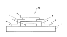
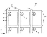
図1は、本発明の第1の実施形態による薄膜トランジスタの断面を模式的に示す図である。図示のとおり、本発明の第1の実施形態による薄膜トランジスタ10は、基板1と、基板1上に形成されたゲート電極2と、基板1上にゲート電極2を覆うように形成されたゲート絶縁膜3と、ゲート絶縁膜3の上面の一部からゲート絶縁膜3の側面に沿って基板1上にまで延びるソース電極4およびドレイン電極5と、ソース電極4およびドレイン電極5のそれぞれの一部とゲート絶縁膜3の上面とに接して形成された半導体活性層6とを含む。
<First Embodiment>
FIG. 1 is a diagram schematically showing a cross section of a thin film transistor according to a first embodiment of the present invention. As illustrated, the
ゲート電極2に印加するゲート電圧によって、ゲート絶縁膜3を介して半導体活性層6に誘起されるチャネル領域が制御され、ソース電極4からチャネル領域を通してドレイン電極5へ流れる電流が制御される。また、薄膜トランジスタ10は、ゲート電圧のオンオフにより、チャネル領域を通してソース電極4とドレイン電極5との間を流れる電流のオンオフを制御するスイッチとして利用することができる。
The channel region induced in the semiconductor
薄膜トランジスタ10は、図1に示すとおり、いわゆるボトムコンタクト構造を有している。ただし、本発明の第1の実施形態にかかる薄膜トランジスタは、これに限定されず、トップコンタクト型であっても良いし、トップ・ボトムコンタクト型であっても良い。さらに、本発明の第1の実施形態にかかる薄膜トランジスタは、基板上に、ソース電極/ドレイン電極、半導体活性層、ゲート絶縁膜、およびゲート電極がこの順に形成されたトップゲート構造を有していても良い。
As shown in FIG. 1, the
基板1は、これらに限定されないが、たとえばポリカーボネイト樹脂、ポリエステル樹脂、ポリアクリレート樹脂、ポリイミド樹脂、ポリエチレンテレフタレート樹脂、ポリエーテルスルフォン樹脂、エポキシ樹脂、ポリメチルメタクリレート樹脂、環状ポリオレフィン樹脂、アモルファスポリオレフィン樹脂、アクリル系UV硬化樹脂などにより、形成される。これらの材料により、基板1は高い柔軟性を有することができる。また、基板1は、上記以外の樹脂で形成されるプラスチック基板、ガラス基板、石英基板、またはシリコン基板であっても良い。 Examples of the substrate 1 include, but are not limited to, polycarbonate resin, polyester resin, polyacrylate resin, polyimide resin, polyethylene terephthalate resin, polyether sulfone resin, epoxy resin, polymethyl methacrylate resin, cyclic polyolefin resin, amorphous polyolefin resin, acrylic It is formed of a system UV curable resin or the like. With these materials, the substrate 1 can have high flexibility. The substrate 1 may be a plastic substrate, a glass substrate, a quartz substrate, or a silicon substrate formed of a resin other than those described above.
ゲート電極2、ソース電極4、およびドレイン電極5は、主に、金、白金、クロム、タングステン、タンタル、ニッケル、銅、アルミニウム、銀、マグネシウム、カルシウムなどの金属により形成されて良い。また、これらの金属の任意の組み合わせによる合金により、これらの電極2、4、5を形成しても良い。さらに、リン(P)や砒素(As)をドーピングした低抵抗ポリシリコンおよびアモルファスシリコン、並びにグラファイトにより、電極2、4、5を形成しても良い。さらにまた、酸化亜鉛、錫添加酸化インジウム(ITO)、インジウム亜鉛酸化物(IZO)などにより、電極2、4、5を形成しても良い。また、導電性高分子材料で電極2、4、5を形成しても良い。
The
また、ゲート電極2、ソース電極4、およびドレイン電極5は、これらに限定されないが、たとえば真空蒸着法、電子ビーム蒸着法、およびRFスパッタ法などの堆積法とリソグラフィ法との組み合わせにより、形成することができる。さらに、選択する材料によっては印刷法により、これらの電極2、4、5を形成しても良い。
The
半導体活性層6は、これらに限定されないが、たとえばペンタセン、アントラセン、テトラセン、ルブレン、フェナントレン、ピレン、クリセン、ペリレン、コロネン、オリゴフェニレン、オリゴチオフェン、ポリチオフェン、ポリアセチレン、ポリアニリン、ポリピロール、ポリフェニレンビニレン、ポリ(2,5−チェニレンビニレン)、ポリ(3−アルキルチオフェン)、ポリ(3−ヘキシルチオフェン)、フルオレン−チオフェンコポリマー、銅フタロシアン、または、これらのフッ素化物もしくは誘導体により形成して良い。また、これらの2又は3以上を任意に組み合わせて、混合して、半導体活性層6を形成しても良い。さらに、半導体活性層6は、上記の材料に限定されず、Si、Ge、GaAs、GaN、GaInN、ZnO、カーボンナノチューブなどの無機系半導体材料により、形成されても良い。
Examples of the semiconductor
また、半導体活性層6は、上記の半導体材料のいずれか又は組み合わせを用いて、真空蒸着法、化学気相堆積法、塗布法、または印刷法などにより、形成することができる。
The semiconductor
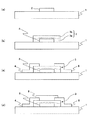
次に、本発明の第1の実施形態による薄膜トランジスタ10におけるゲート絶縁膜3について、図2(a)〜図2(d)を参照しながら、詳細に説明する。なお、これらの図においては、ゲート電極を含めた他の構成を省略する。
Next, the
<ゲート絶縁膜3の第1の例>
図2(a)は、ゲート絶縁膜3の第1の例の断面を示す。図示のとおり、このゲート絶縁膜3は、第1の層3aと、この第1の層3a上に形成された第2の層3bとを有している。第1の層3aおよび第2の層3bは、いずれも無機金属酸化化合物、強誘電性化合物、および希土類金属酸化化合物のうちの少なくとも一つの化合物(以下、説明の便宜上、無機化合物と総称する場合がある)と有機系高分子化合物の混合物により形成される。
<First Example of Gate
FIG. 2A shows a cross section of a first example of the
無機金属酸化化合物には、酸化アルミニウムAl2O3、酸化ビスマスBi2O3、酸化セリウムCeO2、酸化銅CuO、二酸化珪素SiO2、酸化錫SnO2、酸化チタンTiO2、酸化イットリウムY2O3、二酸化ジルコニウムZrO2、酸化亜鉛ZnO、Al2TiO5が含まれるが、これに制限されない。 Inorganic metal oxide compounds include aluminum oxide Al 2 O 3 , bismuth oxide Bi 2 O 3 , cerium oxide CeO 2 , copper oxide CuO, silicon dioxide SiO 2 , tin oxide SnO 2 , titanium oxide TiO 2 , yttrium oxide Y 2 O 3 , zirconium dioxide ZrO 2 , zinc oxide ZnO, Al 2 TiO 5 are included, but not limited thereto.
強誘電性化合物には、BST、Pb(ZrxTi1−x)O3(PZT)、Bi4Ti3O12、BaMgF4、SrBi2(Ta1−xNbx)2O9、Ba(Zr1−xTix)O3(BZT)、BaTiO3、SrTiO3、Bi4Ti3O12、SrBi2Ta2O9、(BaxSr1−x)TiO3、BaMgF4、SrBi2(Ta1−xNbx)2O9、Ba(Zr1−xTix)O3が含まれるが、これに制限されない。
The ferroelectric compounds, BST, Pb (Zr x Ti 1-x) O 3 (PZT), Bi 4 Ti 3
希土類金属酸化化合物には、酸化ジスプロシウムDy2O3、酸化エリビウムEr2O3、酸化ユウロピウムEu2O3、酸化ガドリニウムGd2O3、酸化ホルミウムHo2O3、酸化ランタンLa2O3、酸化ルテチウムLu2O3、酸化ネオジウムNd2O3、酸化プラセオジムPr6O11、酸化スカンジウムSc2O3、酸化サマリウムSm2O3、酸化テルビウムTb4O7、酸化ツリウムTm2O3、酸化イッテルビウムYb2O3、Sb2O3が含まれるが、これに制限されない。 Rare earth metal oxide compounds include dysprosium oxide Dy 2 O 3 , erbium oxide Er 2 O 3 , europium oxide Eu 2 O 3 , gadolinium oxide Gd 2 O 3 , holmium oxide Ho 2 O 3 , lanthanum oxide La 2 O 3 , oxide Lutetium Lu 2 O 3 , neodymium oxide Nd 2 O 3 , praseodymium oxide Pr 6 O 11 , scandium oxide Sc 2 O 3 , samarium oxide Sm 2 O 3 , terbium oxide Tb 4 O 7 , thulium oxide Tm 2 O 3 , ytterbium oxide Yb 2 O 3 and Sb 2 O 3 are included, but not limited thereto.
上述の有機系高分子化合物には、ポリエステル、ポリビニールアルコール、ポリビニールブチラール、ポリアセタール、ポリアリレート、ポリアミド、ポリアミドイミド、ポリエーテルイミド、ポリフェニレンエーテル、ポリフェニレンスルファイド、ポリエーテルスルフォン、ポリエーテルケトン、ポリフタルアミド、ポリエーテルニトリル、ポリベンズイミダゾール、ポリカルボジイミド、ポリシロキサン、ポリメチルメタクリレート、ポリメタクリルアミド、ニトリルゴム、アクリルゴム、ポリエチレンテトラフルオライド、フィノール樹脂、メラミン樹脂、ウレア樹脂、ポリブテン、ポリペンテン、エチル−プロピレン共重合体、エチレン−ブテン−ジエン共重合体、ポリプタジエン、ポリイソプレン、エチレン−プロピレン−シエン共重合体、ポリブタジレン、ポリイソプレン、エチレン−プロピレン−ジエン共重合体、ブチルゴム、ポリメチルペテン、スチレン−ブタジエン共重合体、ポリメチルメタクリレート等のアクリル樹脂、ポリスチレン等のスチレン樹脂、ポリビニールフェノール、カプトンに代表されるポリイミド樹脂、シアノエチル基を有するシアノレジン、ポリカーボネイト樹脂、ポリエステル樹脂、ポリ酢酸ビニル、ポリウレタン樹脂、ポリスルフォン樹脂、エポシキ樹脂、フッ素樹脂、ポリシルセスキオキサン、ポリシロキサン、可溶性ポリイミノド、シクロブタン型ポリイミド、ベンゾフェノン型ポリイミド、BPDA/DPEポリイミド、アゾベンゼンを主鎖に含むポリイミド、長鎖アルキル基を含むポリイミド、含フッ素ポリイミド、液晶性ポリイミド、シンナモイル基、クマリン基、カルコン基、アゾ基のいずれか1つ以上の官能基を有する高分子材料、フェニルマレイミド−スチレン骨格を有する高分子材料、ポリメタクリレート主鎖を有する高分子材料、ポリビニルルシナメート樹脂、ポリパラキシリレン樹脂、ポリメチルメタクリート樹脂、フッ素を含有する高分子材料、セルロース、エポキシアクリレート、ポリアクリロニトリル、ジフェニルエーテルフェノール樹脂、ポリベンゾオキサゾール、ポリベンゾイミダゾール、などのポリマーおよびこれらを組み合わせた化合物を含むが、これに制限はされない。特に、絶縁性に優れたもとのとして、ポリビニールフェノール、ポリアクリルレート、ポリビニールアルコール、フッ素樹脂、シアノエチルプルラン、シアノエチルポリビニールアルコールの高分子材料およびそれらの共重合体が好適である。 The above-mentioned organic polymer compounds include polyester, polyvinyl alcohol, polyvinyl butyral, polyacetal, polyarylate, polyamide, polyamideimide, polyetherimide, polyphenylene ether, polyphenylene sulfide, polyether sulfone, polyether ketone, poly Phthalamide, polyether nitrile, polybenzimidazole, polycarbodiimide, polysiloxane, polymethyl methacrylate, polymethacrylamide, nitrile rubber, acrylic rubber, polyethylene tetrafluoride, finol resin, melamine resin, urea resin, polybutene, polypentene, ethyl -Propylene copolymer, ethylene-butene-diene copolymer, polyptadiene, polyisoprene, ethylene-propylene-sie Copolymers, polybutadylene, polyisoprene, ethylene-propylene-diene copolymers, butyl rubber, polymethylpetene, styrene-butadiene copolymers, acrylic resins such as polymethylmethacrylate, styrene resins such as polystyrene, polyvinylphenol, kapton Polyimide resin, cyanoresin having cyanoethyl group, polycarbonate resin, polyester resin, polyvinyl acetate, polyurethane resin, polysulfone resin, epoxy resin, fluororesin, polysilsesquioxane, polysiloxane, soluble polyimido, cyclobutane type Polyimide, benzophenone type polyimide, BPDA / DPE polyimide, polyimide containing azobenzene in main chain, polyimide containing long chain alkyl group, fluorine-containing polyimide, liquid crystal Polymer material having one or more functional groups of lyimide, cinnamoyl group, coumarin group, chalcone group, azo group, polymer material having phenylmaleimide-styrene skeleton, polymer material having polymethacrylate main chain, polyvinyl Polymers such as lucinamate resin, polyparaxylylene resin, polymethylmethacrylate resin, fluorine-containing polymer material, cellulose, epoxy acrylate, polyacrylonitrile, diphenyl ether phenol resin, polybenzoxazole, polybenzimidazole, etc. Including, but not limited to, combined compounds. In particular, as a material having excellent insulating properties, polyvinyl phenol, polyacrylate, polyvinyl alcohol, fluororesin, cyanoethyl pullulan, cyanoethyl polyvinyl alcohol polymer materials and copolymers thereof are suitable.
再び図2(a)を参照する。第1の層3a中の無機化合物の含有量と第2の層3b中の無機化合物の含有量とが異なるようにゲート絶縁膜3を形成すると、無機化合物の含有量がゲート絶縁膜3の厚さ方向に沿って全体として増加または減少するように変化し、その結果、ゲート絶縁膜3の比誘電率もまた厚さ方向に沿って全体として増加または減少するように変化することとなる。すなわち、第1の層3aと第2の層3bにおける無機化合物の含有量を調整することにより、比誘電率の厚さ方向の分布や変化率をも調整することが可能である。
Reference is again made to FIG. When the
比誘電率を厚さ方向に変化させて比誘電率の高い部分を設けると、比誘電率の低い部分への電界集中を緩和することができる。すなわち、第1の例のゲート絶縁膜3は、薄膜トランジスタ10の絶縁耐性を向上するという効果を有している。
When the portion with a high relative dielectric constant is provided by changing the relative dielectric constant in the thickness direction, the electric field concentration on the portion with a low relative dielectric constant can be reduced. That is, the
さらに、比誘電率を厚さ方向に変化させて比誘電率の傾斜構成とすることで、電気容量の値を自在に制御できるために表示素子駆動に適合したトランジスタ電圧を提供することが可能となる。一般的には、高誘電率の薄膜層をゲート絶縁膜として設ける手法が考えられるが、薄膜層単体のみでは薄膜中のピンホールなどによりリーク電流が発生し絶縁膜として機能しない問題を持つ。本例では、比誘電率を厚さ方向に変化させる、言い換えれば有機高分子材料中の無機化合物の含有量を変化させる構造とすることで、駆動電圧の自在な制御ができ、かつリーク電流の発生の非常に少ないゲート絶縁膜を作製することが可能となる。具体的には、多孔質状の無機化合物からなる薄膜を形成し、その薄膜上に有機高分子材料をコーティングすることで無機化合物と有機高分子材料が混合し、第1のゲート絶縁膜3aを容易に作製できる。さらに、第1のゲート絶縁膜3a上に、多孔質形状が異なる無機化合物の薄膜を更に形成し、この薄膜の上に有機高分子材料をコーティングして形成される第2のゲート絶縁膜の積層構造とすることで、ピンホールなどの欠陥の無い構造で、かつ比誘電率を厚さ方向に変化させた傾斜構成が容易に形成できる。本構造では、ゲート絶縁膜を傾斜構成とすることで同一膜厚で電気容量を自在に制御できるとともに、積層構造とすることでリーク電流の一層の低減を図ることができる有効な機能をもつ。
Furthermore, by changing the relative permittivity in the thickness direction to make the relative permittivity gradient configuration, it is possible to provide a transistor voltage suitable for driving a display element because the value of electric capacity can be freely controlled. Become. In general, a method of providing a thin film layer having a high dielectric constant as a gate insulating film is conceivable. However, a single thin film layer has a problem that a leak current is generated due to pinholes in the thin film and does not function as an insulating film. In this example, by changing the relative dielectric constant in the thickness direction, in other words, by changing the content of the inorganic compound in the organic polymer material, the drive voltage can be freely controlled and the leakage current can be controlled. It is possible to manufacture a gate insulating film with very little occurrence. Specifically, a thin film made of a porous inorganic compound is formed, and an organic polymer material is coated on the thin film, whereby the inorganic compound and the organic polymer material are mixed, and the first
なお、ゲート絶縁膜3(第2の層3b)の上に、表面自由エネルギーが50mJ/m2以下となるコーティング薄膜を形成しても良い。このようなコーティング薄膜は、表面処理層としての役割を担い、この上に形成される半導体活性層6のチャネル領域の成長を制御することが可能となる。この理由について、薄膜上に半導体活性層を成長させる場合、その薄膜の表面自由エネルギーによって、半導体活性層の成長形態が異なることが報告されている(非特許文献4)。ペンタセン半導体材料のような直線上分子の場合には、低い表面自由エネルギーのコーティング薄膜上ではグレインの均一な成長が生じるため、コーティング薄膜−半導体層間の界面でのキャリアのトラップ準位となる欠陥が少ない薄膜成長が可能となり、トランジスタ性能が改善される。具体的には、このコーティング薄膜は、CH3やCF3末端を有する自己組織化単分子膜であり、特にOTS(オクタデシルトリクロロシランCH3(CH2)17SiCl3)やHMDS(ヘキサメチルジシラザン(CH3)3SiNH(CH3)3)が好適である。OTSの表面自由エネルギーは約28mJ/m2であり、HMDSの表面自由エネルギーは約44mJ/m2である。また、このコーティング薄膜は、ポリスチレン、パリレン、またはフッ素樹脂などにより、形成しても良い。上記のいずれのコーティング薄膜によっても、酸化物からなるゲート絶縁膜上に形成される水酸基(-OH)成分を低減することが可能となり、キャリアのトラップ準位の低減が図れるため、トランジスタ性能が大幅に改善される。
Note that a coating thin film having a surface free energy of 50 mJ / m 2 or less may be formed on the gate insulating film 3 (
<ゲート絶縁膜3の第2の例>
図2(b)は、ゲート絶縁膜3の第2の例の断面を示す。図示のとおり、このゲート絶縁膜3は、第1の層3aと、この第1の層3a上に形成された第2の層3bと、第2の層3b上に形成された第3の層3cと、を含む。第1の層3aおよび第2の層3bは、上述の第1の例におけるものと同様である。第3の層3cは、先に列記した有機系高分子化合物のいずれか又は任意の組み合わせにより形成して良い。これにより、ゲート絶縁膜の比誘電率の厚さ方向の変化の割合はより大きくなる。ただし、第3の層3cを第1の層3aおよび第2の層3bと同様に無機化合物と有機系高分子化合物とを含んで形成しても良い。
<Second Example of
FIG. 2B shows a cross section of a second example of the
第2の例のゲート絶縁膜3においても、無機化合物の含有量がゲート絶縁膜3の厚さ方向に沿って変化し、その結果、ゲート絶縁膜3の比誘電率もまた厚さ方向に沿って変化するため、第1の例のゲート絶縁膜3と同じ効果を奏する。
Also in the
なお、第3の層3cの上に先述のコーティング薄膜を形成しても良い。
Note that the above-described coating thin film may be formed on the
<ゲート絶縁膜3の第3の例>
図2(c)は、ゲート絶縁膜3の第3の例の断面を示す。図示のとおり、このゲート絶縁膜3は、第1の部分3dと第2の部分3eとを有している。第1の部分3dは、複数の三角形状の部分が並置されて構成される断面形状(鋸歯状形状)を有している。詳細には、第1の部分3dは、ピラミッド形状をした複数の部分が2次元的に並置されて構成されていて良く、また、三角柱状または円錐状をした部分が一の側面を下にして複数並置されて構成されても良い。一方、第2の部分3eは、第1の部分3dを埋め込むように形成され、その表面は平坦になっている。本例では、第1の部分3dと第2の部分3eとの間の接触面積が増大しているため、平面による接触と比べて緻密に形成でき、信頼性を向上できる。
<Third Example of
FIG. 2C shows a cross section of a third example of the
本例の第1の部分3dは無機化合物により形成されている。すなわち、先に列記した無機金属酸化化合物、強誘電性化合物、および希土類金属酸化化合物のうちの少なくとも一つの化合物により形成されて良い。また、本例の第2の部分3eは、先に列記した有機系高分子化合物のいずれか又は任意の組み合わせにより形成されている。
The
第3の例のゲート絶縁膜3においては、その断面形状からわかるように、無機化合物がゲート絶縁膜3に占める割合が、ゲート絶縁膜3の厚さ方向に沿って連続的または漸近的に変化している。このため、ゲート絶縁膜3の比誘電率もまた厚さ方向に沿って連続的または漸近的に変化しているが、位置によって周期的に変化するため、2次元的に平均した値が代表的な変化となる。したがって、第3の例のゲート絶縁膜3もまた第1の例のゲート絶縁膜3と同じ効果を奏する。
In the
なお、第2の部分3eの上に先述のコーティング薄膜を形成しても良い。
Note that the above-described coating thin film may be formed on the
<ゲート絶縁膜3の第4の例>
図2(d)は、ゲート絶縁膜3の第4の例の断面を示す。図2(c)と対比すると明らかなように、第4の例のゲート絶縁膜3において、第3の例のゲート絶縁膜3と比べて、第1の部分3dが厚く形成されている。その他の点は、第3の例のゲート絶縁膜3と同様である。このため、鋸歯状形状部分において、ゲート絶縁膜3の比誘電率が厚さ方向に沿って連続的に変化している。したがって、第4の例のゲート絶縁膜3もまた第1の例のゲート絶縁膜3と同じ効果を奏する。
<Fourth Example of
FIG. 2D shows a cross section of a fourth example of the
なお、第2の部分3eの上に先述のコーティング薄膜を形成しても良いことも、第3の例と同様である。
Note that the coating thin film described above may be formed on the
また、上記の第1〜第4の例として示したゲート絶縁膜の膜厚は、薄膜トランジスタ10の動作電圧、絶縁耐圧、静電容量の観点から、2μm以下、好ましくは500nm以下、より好ましくは250nm以下が望ましい。
The film thickness of the gate insulating film shown as the first to fourth examples is 2 μm or less, preferably 500 nm or less, more preferably 250 nm from the viewpoint of the operating voltage, dielectric strength, and capacitance of the
以下、実施例を参照しながら、本発明の第1の実施形態による薄膜トランジスタ10を、製造方法と併せ、詳細に説明する。
Hereinafter, the
ゲート絶縁膜3が第1の層3aと第2の層3bとから構成される(図2(a))薄膜トランジスタ10を説明する。
The
(1−1)ゲート電極の形成
まず、ガラス基板を用意し、このガラス基板(基板1)の上にゲート電極2を形成した(図3(a))。具体的には、このゲート電極2は、ガラス基板上に真空蒸着法によりアルミニウム層を形成し、フォトリソグラフィおよびエッチングにより、このアルミニウム層をパターニングして形成した。
(1-1) Formation of Gate Electrode First, a glass substrate was prepared, and a
なお、ゲート電極2は、リフトオフ法により形成しても良いし、所定の開口部形状を有するマスクを用いた真空蒸着法によってアルミニウム層をガラス基板上に堆積することにより形成しても構わない。
The
(1−2)ゲート絶縁膜の形成
(A)上記のゲート電極2と露出したガラス基板との上に、ゲート絶縁膜3の第1の層3aを形成した。具体的には、まず、強誘電性化合物であるチタン酸バリウムBaTiO3(比誘電率1500)の微粒子(直径約20nm以下、TPL社製、NanOxide HPB−1000)を用意し、この微粒子をSDS界面活性剤を含むメチルアルコール溶媒に混入した。その後、超音波ホモジナイザーを用いて、チタン酸バリウム微粒子を含んだメチルアルコール溶液(SDS界面活性剤を含む)から、均一分散液を作製した。なお、この均一分散液中のチタン酸バリウム微粒子の重量比が約5wt%となるよう調整した。
(1-2) Formation of Gate Insulating Film (A) A
次いで、ゲート電極2が形成されたガラス基板1をスピンコータに設置し、当該ガラス基板1上に上記の分散液を所定量滴下し、このガラス基板1を約5000rpmの回転速度で約60秒間回転することにより、チタン酸バリウムと溶媒等を含む膜を形成した。その後、この膜が形成されたガラス基板1を真空オーブン中で約100℃の温度で約30分間ベーキングして、チタン酸バリウムを含む強誘電性化合物層を得た。なお、電子顕微鏡を用いた観察から、この強誘電性化合物層は多孔質状であることが分かった。
Next, the glass substrate 1 on which the
続けて、シアノエチレンポリビニールアルコール(信越化学製、シアノレジンCR−V)と熱架橋剤PMFM(Aldrich製、Poly (melamine - co - formaldehyde) methylated)とを4:1の重量比でDMF溶媒中に溶解させ、シアノエチレンポリビニールアルコール溶液を作製した。次に、この溶液を上記の強誘電性化合物層上にディップコートし、空気中で約80℃の温度で約30分プリベーキングし、さらに、真空オーブン中で150℃の温度で約4時間ベーキングして、シアノエチルポリビニールアルコールを含む有機高分子材料層を得た。このようなベーキング処理により、3次元的な熱架橋反応が促進され、緻密な絶縁膜が得られる。以上の手順により、第1の層3aが形成された。第1の層3aの厚さは約80nmであった。
Subsequently, cyanoethylene polyvinyl alcohol (manufactured by Shin-Etsu Chemical Co., Ltd., cyanoresin CR-V) and thermal crosslinking agent PMFM (manufactured by Aldrich, Poly (melamine-co-formaldehyde) methylated) in a DMF solvent at a weight ratio of 4: 1. It was dissolved to prepare a cyanoethylene polyvinyl alcohol solution. Next, this solution is dip-coated on the above ferroelectric compound layer, prebaked in air at a temperature of about 80 ° C. for about 30 minutes, and further baked in a vacuum oven at a temperature of 150 ° C. for about 4 hours. Thus, an organic polymer material layer containing cyanoethyl polyvinyl alcohol was obtained. By such baking treatment, a three-dimensional thermal crosslinking reaction is promoted, and a dense insulating film can be obtained. The
なお、第1の層3aを電子顕微鏡で観察したところ、多孔質状の強誘電性化合物層の空隙が有機化合物により埋められていることが分かった。
In addition, when the
(B)次に、第1の層3aの上に第2の層3bを形成した。第2の層3bの形成手順は、均一分散液中のチタン酸バリウム微粒子の重量比を約2wt%と変更した点を除き、第1の層3aの形成手順と同じである。すなわち、形成した第2の層3bは、チタン酸バリウムとシアノエチルポリビニールアルコールを含んでいる。また、第2の層3bの厚さは約50nmであった。第2の層3bの厚さが第1の層3aの厚さ(80nm)より薄いのは、均一分散液中のチタン酸バリウム微粒子の重量比が低い(チタン酸バリウム密度が疎な)ためである。
(B) Next, the
続いて、第1の層3aおよび第2の層3bが所定の形状を有するようにパターニングすることにより、ゲート絶縁膜3が形成された(図3(b))。
Subsequently, the
なお、上述の第1の層3aと第2の層3bとをそれぞれ個別に形成し、その上にアルミニウム電極を蒸着して電気的評価を評価したところ、図4に示す結果が得られた。この結果から、薄膜トランジスタ10のゲート絶縁膜3として極めて良好な比誘電率および絶縁耐圧が得られたことが分かる。これは、分散液を利用して多孔質状の強誘電性化合物層を形成しているため、ゲート絶縁膜3中の強誘電性化合物の含有量を増大することができることによると考えられる。また、本実施例においては、第2の層3bの比誘電率は、その下に形成されている第1の層3aの比誘電率よりも低いため(図4参照)、ゲート絶縁膜3の比誘電率は、ゲート電極2から半導体活性層6へ向かう方向に沿って低くなっている。ただし、これとは逆に、ゲート絶縁膜3の比誘電率がゲート電極2から半導体活性層6へ向かう方向に沿って高くなる他の実施例も考えられる。
In addition, when the above-mentioned
(1−3)ソース電極およびドレイン電極の形成
次いで、ゲート絶縁膜3とガラス基板1の上に真空蒸着法によって金を堆積し、フォトリソグラフィおよびエッチングにより、ソース電極4およびドレイン電極5を形成した(図3(c))。これらの電極4、5の厚さは、約50nmであった。
(1-3) Formation of Source Electrode and Drain Electrode Next, gold was deposited on the
なお、ソース電極4およびドレイン電極5は、ゲート絶縁膜3とガラス基板1の上に所定のパターンを有するフォトレジスト層を形成し、その上から真空蒸着法により金を堆積し、リフトオフ法によって形成しても良い。
The source electrode 4 and the
(1−4)半導体活性層の形成
ソース電極4およびドレイン電極5の形成後、真空蒸着法により、ペンタセンからなる半導体活性層6を形成した。真空蒸着法において、ペンタセンの堆積速度を約0.03〜0.04nm/秒とし、膜厚が約50nmとなるよう堆積時間を調整した。また、真空蒸着の際には、所定の形状の開口部を有するマスクを用いて、半導体活性層6を所定の形状に形成した(図3(d))。
(1-4) Formation of Semiconductor Active Layer After the source electrode 4 and the
以上の手順により、薄膜トランジスタ10が得られた。以下、説明の便宜上、この薄膜トランジスタ10をトランジスタ101と称す。
Through the above procedure, the
実施例2の薄膜トランジスタ10は、実施例1のトランジスタ101に比べ、ゲート絶縁膜の材料が相違し、他の構成は同一である。
The
(2−1)ゲート電極の形成
まず、ガラス基板1上にゲート電極2を形成する。この形成方法は、上述の「(1−1)ゲート電極の形成」で説明したとおりである。
(2-1) Formation of Gate Electrode First, the
(2−2)ゲート絶縁膜の形成
(A)次に、上記のゲート電極2と露出したガラス基板との上に、ゲート絶縁膜3の第1の層3aを形成した。具体的には、まず、金属酸化化合物である酸化ジルコニウムZrO2(比誘電率25)の微粒子(直径約20nm以下、NanoTek社製)を用意し、この微粒子を分散剤を含むジメチルアセトアミド溶媒に混入した。その後、超音波ホモジナイザーを用いて、酸化ジルコニウム微粒子を含むメチルアセトアミド溶液(分散剤を含む)から、均一分散液を作製した。なお、この均一分散液中の酸化ジルコニウムの重量比は、約10wt%であった。
(2-2) Formation of Gate Insulating Film (A) Next, the
次いで、ゲート電極2が形成されたガラス基板1上に上記の分散液を所定量滴下し、このガラス基板1を約6000rpmの回転速度で約60秒間回転することにより、酸化ジルコニウムと溶媒等を含む膜を形成した。その後、この膜が形成されたガラス基板1を真空オーブン中で約100℃の温度で約30分間ベーキングして、酸化ジルコニウムを含む金属酸化化合物層を得た。
Next, a predetermined amount of the above dispersion is dropped onto the glass substrate 1 on which the
続けて、ポリビニールフェノール(Aldrich製、分子量20,000)と熱架橋剤PMFM(Aldrich製、Poly (melamine - co - formaldehyde)methylated)とを4:1の重量比でPGMEA(Propylene Glycol Methyl Ether Acetate、Aldrich製)溶媒中に溶解させ、ポリビニールフェノール溶液を作製した。次に、この溶液を上記の金属酸化化合物層上にディップコートし、空気中で約80℃の温度で約30分プリベーキングし、さらに、真空オーブン中で180℃の温度で約1時間ベーキングして、ポリビニールフェノールを含む有機化合物層を得た。これにより、第1の層3aが形成された。この第1の層3aの厚さは、約90nmであった。
Subsequently, PGMEA (Propylene Glycol Methyl Ether Acetate) was used in a weight ratio of 4: 1 between polyvinylphenol (Aldrich, molecular weight 20,000) and thermal crosslinking agent PMFM (Aldrich, Poly (melamine-co-formaldehyde) methylated). (Manufactured by Aldrich) was dissolved in a solvent to prepare a polyvinyl phenol solution. Next, the solution is dip-coated on the metal oxide compound layer, pre-baked in air at a temperature of about 80 ° C. for about 30 minutes, and further baked in a vacuum oven at a temperature of 180 ° C. for about 1 hour. Thus, an organic compound layer containing polyvinyl phenol was obtained. Thereby, the
(B)次に、均一分散液中の酸化ジルコニウム微粒子の重量比を約2wt%と変更し、その他の条件を同じままとして、第1の層3aの上に第2の層3bを形成した。第2の層3bの厚さは、第1の層3a(約90nm)よりも薄い約40nmであった。
(B) Next, the
以上の手順により、ゲート絶縁膜3が形成された。
The
なお、上述の第1の層3aと第2の層3bとをそれぞれ個別に形成し、その上にアルミニウム電極を蒸着して電気的評価を評価したところ、図4に示す結果が得られた。この結果から、薄膜トランジスタ10のゲート絶縁膜3として極めて良好な比誘電率および絶縁耐圧が得られたことが分かる。
In addition, when the above-mentioned
続いて、実施例1で説明した(1−3)と(1―4)の手順を行って、薄膜トランジスタ10を得た。以下、説明の便宜上、この薄膜トランジスタ10をトランジスタ102と称す。
Subsequently, the steps (1-3) and (1-4) described in Example 1 were performed to obtain the
実施例3では、ゲート絶縁膜3が第1の部分3dと第2の部分3eとから構成される(図2(c))薄膜トランジスタ10を説明する。
In Example 3, a
(3−1)ゲート電極の形成
まず、上述の「(1−1)ゲート電極の形成」で説明したように、ガラス基板1上にゲート電極2を形成する。
(3-1) Formation of Gate Electrode First, as described in “(1-1) Formation of Gate Electrode” above, the
(3−2)ゲート絶縁膜の形成
(A)次に、上記のゲート電極2と露出したガラス基板との上に、ゲート絶縁膜3の第1の層3aを形成した。具体的には、まず、金属酸化化合物である酸化チタンTiO2の微粒子(ルチル構造、比誘電率100、微粒子直径10nm、NanoTek製)を用意し、この微粒子を分散剤を含むイソプロピルアルコールIPA溶媒に混入した。その後、超音波ホモジナイザーを用いて、酸化チタン微粒子を含んだメチルアルコール溶液(分散剤を含む)から、均一分散液を作製した。なお、この均一分散液中の酸化チタン微粒子の重量比を約5wt%となるよう調整した。
(3-2) Formation of Gate Insulating Film (A) Next, the
次いで、ゲート電極2が形成されたガラス基板1上に上記の分散液を所定量滴下して分散液の膜をスピンコートした。その後、スピンコートした膜に対して、三角形状の断面(深さ100nm、繰り返し周期100nm)を有するスタンプを押圧し、このままの状態で、真空オーブン中で100℃で30分間ベーキングを行った。室温にまで冷却した後、スタンプを除去し、第1の部分3d(酸化チタン膜)を得た。
Next, a predetermined amount of the above dispersion was dropped onto the glass substrate 1 on which the
なお、予備実験から、このようなスタンプにより、図2(c)または図2(d)に示す第1の部分3dと同じ断面形状が得られることが確認されている。
From preliminary experiments, it has been confirmed that such a stamp can provide the same cross-sectional shape as the
(B)引き続き、第1の部分3dの上に、フッ素系樹脂(比誘電率は約2.1、旭硝子製、Cytop)液をスピンコートし、空気中にて、約50℃で30分間、約80℃で30分間、続けて約120℃で2時間、ベーキングした。これにより、緻密かつ表面平坦性に優れた絶縁膜(第2の部分3e)を得た。本実施例のゲート絶縁膜3の厚さ(第1の部分3dと第2の部分3eとの合計)は、約200nmであった。
(B) Subsequently, a fluorine-based resin (relative permittivity is about 2.1, manufactured by Asahi Glass Co., Ltd., Cytop) is spin-coated on the
なお、本実施例のゲート絶縁膜3を別途形成し、その上にアルミニウム電極を蒸着して電気的評価を評価したところ、図4に示す結果が得られた。この結果から、薄膜トランジスタ10のゲート絶縁膜3として極めて良好な比誘電率および絶縁耐圧が得られたことが分かる。
In addition, when the
続いて、実施例1で説明した(1−3)と(1―4)の手順を行って、薄膜トランジスタ10を得た。以下、説明の便宜上、実施例3の薄膜トランジスタ10をトランジスタ103と称す。
Subsequently, the steps (1-3) and (1-4) described in Example 1 were performed to obtain the
実施例4の薄膜トランジスタは、実施例2の薄膜トランジスタ10(トランジスタ102)におけるゲート絶縁膜3の上にフッ素樹脂薄膜が形成されている点で、実施例2の薄膜トランジスタ10と相違し、他の構成は同様である。このフッ素樹脂薄膜(厚さ約5nm)は、ゲート絶縁膜3(第2の層3b)の形成後に、ゲート絶縁膜3の上にフッ素系樹脂(旭硝子製、Cytop)液をディップコートすることにより形成した。その他の製造手順は、実施例2で説明したとおりである。実施例4の薄膜トランジスタを、便宜上、トランジスタ104と称す。
The thin film transistor of the fourth embodiment is different from the
実施例5の薄膜トランジスタは、実施例2の薄膜トランジスタ10(トランジスタ102)におけるゲート絶縁膜3の上に自己組織化単分子膜(HMDS)が形成されている点で、実施例2の薄膜トランジスタ10と相違し、他の構成は同様である。この自己組織化単分子膜は、ゲート絶縁膜3(第2の層3b)の形成後に、ゲート絶縁膜3の上にHMDSをスピンコートすることにより形成した。その他の製造手順は、実施例2で説明したとおりである。実施例5の薄膜トランジスタを、便宜上、トランジスタ105と称す。
The thin film transistor of Example 5 is different from the
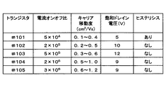
上述のトランジスタ101〜105の電気的特性の一例を図5に示す。この図から分かるとおり、トランジスタ101〜105は、高いキャリア移動度を有している。また、トランジスタ101〜105は、約12Vといった低い動作電圧で動作することが確認されており、優れた電気的特性を有していることが分かった。なお、図5から分かるように、トランジスタ104および105においては、トランジスタ101〜103に比べて、キャリア移動度が高くなる傾向が見られる。この結果から、トランジスタ104および105が有するコーティング薄膜の効果が理解される。
An example of the electrical characteristics of the above-described transistors 101 to 105 is shown in FIG. As can be seen from this figure, the transistors 101 to 105 have high carrier mobility. In addition, it was confirmed that the transistors 101 to 105 operate at a low operating voltage such as about 12 V, and it was found that the transistors 101 to 105 have excellent electrical characteristics. As can be seen from FIG. 5, the
本発明の実施例にかかる薄膜トランジスタは、無機化合物と有機高分子材料とを含むゲート絶縁膜を有しているため、実施例1〜5において説明したように、そのゲート絶縁膜を約180℃といった低温にて形成することができる。しかも、この薄膜トランジスタは、実用上、優れた電気的特性を有している。したがって、本発明の実施例によれば、基板にプラスチック基板を用いた場合でも、動作性能に優れた薄膜トランジスタを得ることができる。 Since the thin film transistor according to the example of the present invention has a gate insulating film containing an inorganic compound and an organic polymer material, the gate insulating film is about 180 ° C. as described in Examples 1 to 5. It can be formed at a low temperature. Moreover, this thin film transistor has practically excellent electrical characteristics. Therefore, according to the embodiment of the present invention, even when a plastic substrate is used as the substrate, a thin film transistor excellent in operating performance can be obtained.
<第2の実施形態>
図6は、本発明の第2の実施形態によるアクティブマトリックス構造体の模式的な上面図である。図示のとおり、本実施形態のアクティブマトリックス構造体100は、X方向に延びる複数の走査線24と、Y方向に延びる複数の信号線22と、複数の走査線と複数の信号線との各交差点に隣接して配置される薄膜トランジスタ26とを有している。この薄膜トランジスタ26は、本発明の第1の実施形態による薄膜トランジスタ(10、101〜105)であって良い。また、薄膜トランジスタ26のゲート電極2は走査線24と接続し、ソース電極4が信号線22と接続している。
<Second Embodiment>
FIG. 6 is a schematic top view of an active matrix structure according to the second embodiment of the present invention. As illustrated, the
また、本実施形態のアクティブマトリックス構造体100は、信号線22と走査線24とで囲まれる領域に画素電極28を有している。画素電極28は、薄膜トランジスタ26のドレイン電極5と電気的に接続している。また、画素電極28は、信号線22と走査線24とで囲まれる領域に配置されるエレクトロルミネッセンス(EL)素子の電極を兼ねる。
In addition, the
アクティブマトリックス構造体100は、たとえば、以下のようにして製造することができる。
The
まず、ガラスやプラスチックなどで形成された基板1(図7参照)の上に厚さが約50nmのクロム膜をスパッタリング法により成膜し、フォトリソグラフィ法およびエッチング法により、走査線24と薄膜トランジスタ26のゲート電極2とを形成する。基板の寸法は、製造するアクティブマトリックス構造体100に応じて適宜決定して良く、また、走査線24の間隔は、アクティブマトリックス構造体100が適用される表示装置(後述)の画素密度に応じて適宜決定して良い。
First, a chromium film having a thickness of about 50 nm is formed on a substrate 1 (see FIG. 7) made of glass, plastic, or the like by sputtering, and the
次に、薄膜トランジスタ26のゲート絶縁膜が形成される。このゲート絶縁膜は、第1の実施形態として説明した薄膜トランジスタ10のいずれかのゲート絶縁膜3であって良く、典型的には、実施例2で説明した酸化ジルコニウムとポリビニールフェノールとを含むゲート絶縁膜であって良い。また、その形成方法も、実施例2で説明したとおりであって良い。ゲート絶縁膜を形成した後、インジウム錫酸化物(ITO)により画素電極28が形成される。
Next, a gate insulating film of the
続いて、ソース電極4とドレイン電極5が形成される。具体的には、所定の開口部を有するマスクを用いて、真空蒸着法またはスパッタリング法により、金膜または金/クロム膜を形成することにより、ソース電極4とドレイン電極5を形成することができる。
Subsequently, the source electrode 4 and the
次に、上記のゲート絶縁膜上であってソース電極4とドレイン電極5と結合するように、薄膜トランジスタ26の活性層が形成される。具体的には、所定の開口部を有するマスクを用いた真空蒸着法により、有機半導体であるペンタセンを堆積することにより、活性層を形成することができる。また、ペンタセンに替わり、ポリチオフェン等の高分子半導体層をスピンコート法などの塗布法により形成し、フォトリソグラフィ法およびエッチング法により活性層を形成しても良い。
Next, an active layer of the
上述した活性層までの各要素が形成された基板1上にパリレンによるパッシベーション膜32(図7参照)を形成することにより、アクティブマトリックス構造体100が完成する。なお、パリレンに替わり、サイトップ(旭硝子製)などのフッ素樹脂によりパッシベーション膜32を形成しても良い。
An
本発明の第2の実施形態によるアクティブマトリックス100は、本発明の第1の実施形態による薄膜トランジスタ(10、101〜105)と同じ薄膜トランジスタ26を含むため、低い動作電圧で動作することができるという利点を有している。
The
<第3の実施形態>
図7は、本発明の第3の実施形態による表示装置の断面図である。図示のとおり、この表示装置200は、第2の実施形態によるアクティブマトリックス構造体100と、アクティブマトリックス構造体100のパッシベーション膜32の上方に設けられる表示素子形成領域33と、表示素子領域33の上に形成される透明電極34と、透明電極34上に設けられる上部基板36と、を含む。上部基板36は、典型的には、ガラス、およびポリエステル、ポリカーボネイト、ポリアリレート、ポリエーテルスルフォンなどのプラスチックにより、形成して良い。
<Third Embodiment>
FIG. 7 is a cross-sectional view of a display device according to the third embodiment of the present invention. As illustrated, the
表示素子領域33には、EL素子、好ましくは有機EL素子が形成され、これにより、本発明の第2の実施形態によるアクティブマトリックス構造体100を利用したEL表示装置が得られる。このEL素子は、アクティブマトリックス構造体100の画素電極28に対応して設けられ、画素電極28と透明電極34とにより、電極の供給を受けて光を発する。また、薄膜トランジスタ26はドレイン電極5で画素電極28と結合しており、薄膜トランジスタ26のオンオフ動作により、EL素子がスイッチングされる。したがって、図6に示すようにマトリックス状に設けられた複数の薄膜トランジスタのうちの所定のものをオンとすることにより、このEL表示装置により、所定の画像が表示される。
In the
また、表示素子領域33に画素電極28と透明電極34と結合するように液晶素子を形成することにより、本発明の第2の実施形態によるアクティブマトリックス構造体100を利用した液晶パネルを製造することもできる。
In addition, a liquid crystal panel using the
さらに、表示素子領域33に画素電極28と透明電極34と結合するように電気泳動素子を形成することにより、本発明の第2の実施形態によるアクティブマトリックス構造体100を利用した電気泳動表示パネルを製造することも可能である。
Furthermore, an electrophoretic display panel using the
本発明の第3の実施形態による表示装置200は、表示装置200のアクティブマトリックス100が、本発明の第1の実施形態による薄膜トランジスタ(10、101〜105)と同じ薄膜トランジスタ26を含むため、低い動作電圧で動作することができる。また、薄膜トランジスタ26を始めとして、低いプロセス温度にて形成することができるため、柔軟性を有するプラスチック基板を使用すれば、柔軟性を有する表示装置を提供することも可能となる。
The
以上、幾つかの実施形態および実施例を参照しながら、本発明にかかる薄膜トランジスタを詳細に説明したが、本発明は、上記の実施形態および実施例に限定されることなく、種々に変形可能である。 As described above, the thin film transistor according to the present invention has been described in detail with reference to some embodiments and examples. However, the present invention is not limited to the above embodiments and examples, and can be variously modified. is there.
本発明の実施形態にかかる薄膜トランジスタは、上述したように、アクティブマトリックス構造体やこれを用いた表示素子に好適であるが、用途はこれらに限られない。たとえば、本発明の実施形態にかかる薄膜トランジスタは、電子メモリ装置への適用も可能である。特に、実施例1のトランジスタ101は、図5に示すとおり、大きなヒステリシスを有するため、電子メモリ素子として有望である。 As described above, the thin film transistor according to the embodiment of the present invention is suitable for an active matrix structure and a display element using the active matrix structure, but the application is not limited thereto. For example, the thin film transistor according to the embodiment of the present invention can be applied to an electronic memory device. In particular, the transistor 101 of Example 1 is promising as an electronic memory element because it has a large hysteresis as shown in FIG.
実施例1〜5において、ゲート絶縁膜を形成する際に、いくつかの無機化合物の微粒子を用いることを説明したが、これらの実施例で説明した無機化合物に限ることなく、先に列記した無機化合物のいずれか又はこれらの任意の組み合わせを利用できることは言うまでもない。 In Examples 1 to 5, it has been described that fine particles of some inorganic compounds are used when forming the gate insulating film. However, the inorganic compounds listed above are not limited to the inorganic compounds described in these Examples. Of course, any of the compounds or any combination thereof can be utilized.
また、ゲート絶縁膜3の第1の例、並びに実施例1および2において、ゲート絶縁膜3が2つの層から構成される場合を例示したが、これに限らず、3層以上であっても良い。ゲート絶縁膜3を3層以上で構成し、各層における無機化合物の含有量を積層順に段階的に変化させることにより、ゲート絶縁膜3内の比誘電率をその厚さ方向に沿ってより滑らかに変化させることが可能となり、また、より大きい範囲で比誘電率を変化させることが可能となる。
Further, in the first example of the
また、実施例1〜5において、約20nm(チタン酸バリウム)、約20nm(酸化ジルコニウム)、約10nm(酸化チタン)といった直径を有する微粒子を例示したが、微粒子の直径は、これらの値に限定されることはない。分散液中での均一な分散、ゲート絶縁膜中の含有量の制御性、ゲート絶縁膜の薄膜化および均一性の観点から微粒子の直径は1μm以下が好ましい。また、微粒子の直径が200nm以下または50nm以下であるとより好ましい。 In Examples 1 to 5, fine particles having diameters of about 20 nm (barium titanate), about 20 nm (zirconium oxide), and about 10 nm (titanium oxide) are exemplified, but the diameter of the fine particles is limited to these values. It will never be done. From the viewpoints of uniform dispersion in the dispersion, controllability of the content in the gate insulating film, thinning of the gate insulating film, and uniformity, the diameter of the fine particles is preferably 1 μm or less. The diameter of the fine particles is more preferably 200 nm or less or 50 nm or less.
実施例1〜5においては、スピンコート法やディップコート法を利用してゲート絶縁膜3を形成したが、ゲート絶縁膜3は、これらに限らず、たとえば、キャスティング、ブレードコーティング、ワイヤバーコーティング、スプレーコーティング、ロールコーティングなどのコーティング法、インクジェット印刷、スクリーン印刷、オフセット印刷、凸版印刷などの印刷法、マイクロコンタクトプリンティングなどのソフトリソグラフィー法、若しくはナノインプラント法、またはこれらの手法の2又は3以上を任意に組み合わせた方法によって、形成しても良い。
In Examples 1-5, although the
さらに、無機化合物により形成される第1の部分3dの形状は、無機化合物がゲート絶縁膜中に占める割合がゲート絶縁膜の厚さ方向に沿って変化する形状である限りにおいて、三角形状(断面)に限られず、たとえば正弦波形状であって良いし、複数のピラミッドあるいは円錐が並置される形状であっても良い。
Further, the
また、上述のとおり、本発明の実施形態による薄膜トランジスタは、ボトムコンタクト構造に限らず、他の構造を有することができる。特に、半導体活性層6の上にゲート絶縁膜を形成する場合、上記のゲート絶縁膜3の第3の例における第1の部分3dを半導体活性層6上に形成して良い。
Further, as described above, the thin film transistor according to the embodiment of the present invention is not limited to the bottom contact structure, and may have other structures. In particular, when a gate insulating film is formed on the semiconductor
1 基板、2 ゲート電極、3 ゲート絶縁膜、4 ソース電極、5 ドレイン電極、6 半導体活性層、10 薄膜トランジスタ、22 信号線、24 走査線、26 薄膜トランジスタ、28 画素電極、32 パッシベーション膜、34 透明電極、36 上部電極、100 アクティブマトリックス構造体、200 表示装置。
DESCRIPTION OF SYMBOLS 1 Substrate, 2 Gate electrode, 3 Gate insulating film, 4 Source electrode, 5 Drain electrode, 6 Semiconductor active layer, 10 Thin film transistor, 22 Signal line, 24 Scan line, 26 Thin film transistor, 28 Pixel electrode, 32 Passivation film, 34
Claims (9)
前記活性層に結合するソース電極;
前記活性層に結合し、前記活性層を通して前記ソース電極と導通可能なドレイン電極;
前記活性層に結合し、有機高分子材料と無機化合物とが混合された層が複数層積層されて構成されるゲート絶縁膜;および
前記ゲート絶縁膜に接し、該ゲート絶縁膜を介して前記活性層にチャネル領域を形成できるよう構成されるゲート電極;
を備える薄膜トランジスタ。 An active layer formed of a semiconductor material;
A source electrode coupled to the active layer;
A drain electrode coupled to the active layer and capable of conducting with the source electrode through the active layer;
A gate insulating film formed by laminating a plurality of layers in which an organic polymer material and an inorganic compound are mixed and bonded to the active layer; and the active layer through the gate insulating film in contact with the gate insulating film; A gate electrode configured to form a channel region in the layer;
A thin film transistor comprising:
無機化合物の微粒子を用意するステップと、
前記微粒子を溶媒に混入して分散液を作製するステップと、
前記分散液を用いて前記無機化合物層を形成するステップと、
前記第1の膜上に前記有機高分子材料層を形成するステップと、
を有する、前記ゲート絶縁膜を形成する工程を含む方法。 A method for producing the thin film transistor according to any one of claims 1 to 7,
Preparing fine particles of an inorganic compound;
Mixing the fine particles in a solvent to produce a dispersion;
Forming the inorganic compound layer using the dispersion;
Forming the organic polymer material layer on the first film;
Forming the gate insulating film.
前記第1の方向と交差する第2の方向に延びる複数の走査線;
前記複数の信号線と前記複数の走査線との各交差点に隣接して配置され、ゲート電極が前記走査線と接続し、ソース電極が前記信号線と接続する、請求項1から8のいずれか一項に記載の薄膜トランジスタ;
前記薄膜トランジスタのドレイン電極と結合する表示素子;および
前記表示素子と結合し、前記ドレイン電極とともに前記表示素子へ電力を印加することができるよう設けられた電極;
を含む表示装置。 A plurality of signal lines extending along the first direction;
A plurality of scan lines extending in a second direction intersecting the first direction;
9. The semiconductor device according to claim 1, wherein the gate electrode is connected to the scanning line, and the source electrode is connected to the signal line. The gate electrode is connected to each intersection of the plurality of signal lines and the plurality of scanning lines. The thin film transistor according to one item;
A display element coupled to the drain electrode of the thin film transistor; and an electrode coupled to the display element and provided to be able to apply power to the display element together with the drain electrode;
Display device.
Priority Applications (1)
| Application Number | Priority Date | Filing Date | Title |
|---|---|---|---|
| JP2008316256A JP2010141142A (en) | 2008-12-11 | 2008-12-11 | Thin film transistor and method of manufacturing the same, and display device |
Applications Claiming Priority (1)
| Application Number | Priority Date | Filing Date | Title |
|---|---|---|---|
| JP2008316256A JP2010141142A (en) | 2008-12-11 | 2008-12-11 | Thin film transistor and method of manufacturing the same, and display device |
Publications (1)
| Publication Number | Publication Date |
|---|---|
| JP2010141142A true JP2010141142A (en) | 2010-06-24 |
Family
ID=42351008
Family Applications (1)
| Application Number | Title | Priority Date | Filing Date |
|---|---|---|---|
| JP2008316256A Pending JP2010141142A (en) | 2008-12-11 | 2008-12-11 | Thin film transistor and method of manufacturing the same, and display device |
Country Status (1)
| Country | Link |
|---|---|
| JP (1) | JP2010141142A (en) |
Cited By (5)
| Publication number | Priority date | Publication date | Assignee | Title |
|---|---|---|---|---|
| JP2011233587A (en) * | 2010-04-23 | 2011-11-17 | Seiko Epson Corp | Organic transistor and method for manufacturing the same |
| JP2011258894A (en) * | 2010-06-11 | 2011-12-22 | Fuji Xerox Co Ltd | Field effect organic transistor |
| WO2012014786A1 (en) * | 2010-07-30 | 2012-02-02 | Semiconductor Energy Laboratory Co., Ltd. | Semicondcutor device and manufacturing method thereof |
| KR20150059884A (en) * | 2013-11-25 | 2015-06-03 | 엘지디스플레이 주식회사 | Method for manufacturing organic light emitting display device |
| TWI678798B (en) * | 2018-06-07 | 2019-12-01 | 國立成功大學 | High-sensitivity organic light sensor and manufacturing method thereof |
Citations (7)
| Publication number | Priority date | Publication date | Assignee | Title |
|---|---|---|---|---|
| JP2002110999A (en) * | 2000-09-29 | 2002-04-12 | Toshiba Corp | Transistor and manufacturing method thereof |
| JP2005072569A (en) * | 2003-08-06 | 2005-03-17 | Mitsubishi Chemicals Corp | Organic field effect transistor |
| JP2006173532A (en) * | 2004-12-20 | 2006-06-29 | Nippon Hoso Kyokai <Nhk> | Organic transistor and method for forming organic transistor |
| JP2006190923A (en) * | 2004-12-06 | 2006-07-20 | Toppan Printing Co Ltd | Thin film transistor |
| JP2006332661A (en) * | 2005-05-24 | 2006-12-07 | Samsung Sdi Co Ltd | ORGANIC THIN FILM TRANSISTOR, ITS MANUFACTURING METHOD, AND ORGANIC ELECTROLUMINESCENT DISPLAY DEVICE HAVING ORGANIC THIN FILM TRANSISTOR |
| JP2007180131A (en) * | 2005-12-27 | 2007-07-12 | Matsushita Electric Ind Co Ltd | Organic FET and manufacturing method thereof |
| JP2009182299A (en) * | 2008-02-01 | 2009-08-13 | Konica Minolta Holdings Inc | Organic thin film transistor manufacturing method and organic thin film transistor |
-
2008
- 2008-12-11 JP JP2008316256A patent/JP2010141142A/en active Pending
Patent Citations (7)
| Publication number | Priority date | Publication date | Assignee | Title |
|---|---|---|---|---|
| JP2002110999A (en) * | 2000-09-29 | 2002-04-12 | Toshiba Corp | Transistor and manufacturing method thereof |
| JP2005072569A (en) * | 2003-08-06 | 2005-03-17 | Mitsubishi Chemicals Corp | Organic field effect transistor |
| JP2006190923A (en) * | 2004-12-06 | 2006-07-20 | Toppan Printing Co Ltd | Thin film transistor |
| JP2006173532A (en) * | 2004-12-20 | 2006-06-29 | Nippon Hoso Kyokai <Nhk> | Organic transistor and method for forming organic transistor |
| JP2006332661A (en) * | 2005-05-24 | 2006-12-07 | Samsung Sdi Co Ltd | ORGANIC THIN FILM TRANSISTOR, ITS MANUFACTURING METHOD, AND ORGANIC ELECTROLUMINESCENT DISPLAY DEVICE HAVING ORGANIC THIN FILM TRANSISTOR |
| JP2007180131A (en) * | 2005-12-27 | 2007-07-12 | Matsushita Electric Ind Co Ltd | Organic FET and manufacturing method thereof |
| JP2009182299A (en) * | 2008-02-01 | 2009-08-13 | Konica Minolta Holdings Inc | Organic thin film transistor manufacturing method and organic thin film transistor |
Cited By (8)
| Publication number | Priority date | Publication date | Assignee | Title |
|---|---|---|---|---|
| JP2011233587A (en) * | 2010-04-23 | 2011-11-17 | Seiko Epson Corp | Organic transistor and method for manufacturing the same |
| JP2011258894A (en) * | 2010-06-11 | 2011-12-22 | Fuji Xerox Co Ltd | Field effect organic transistor |
| WO2012014786A1 (en) * | 2010-07-30 | 2012-02-02 | Semiconductor Energy Laboratory Co., Ltd. | Semicondcutor device and manufacturing method thereof |
| US9559211B2 (en) | 2010-07-30 | 2017-01-31 | Semiconductor Energy Laboratory Co., Ltd. | Semiconductor device and manufacturing method thereof |
| KR20150059884A (en) * | 2013-11-25 | 2015-06-03 | 엘지디스플레이 주식회사 | Method for manufacturing organic light emitting display device |
| KR101616929B1 (en) | 2013-11-25 | 2016-04-29 | 엘지디스플레이 주식회사 | Method for manufacturing organic light emitting display device |
| US9461270B2 (en) | 2013-11-25 | 2016-10-04 | Lg Display Co., Ltd. | Method for manufacturing organic light emitting diode display device |
| TWI678798B (en) * | 2018-06-07 | 2019-12-01 | 國立成功大學 | High-sensitivity organic light sensor and manufacturing method thereof |
Similar Documents
| Publication | Publication Date | Title |
|---|---|---|
| US11177465B2 (en) | Devices, structures, materials and methods for vertical light emitting transistors and light emitting displays | |
| KR101943595B1 (en) | Active matrix dilute source enabled vertical organic light emitting transistor | |
| US7485576B2 (en) | Method of forming conductive pattern, thin film transistor, and method of manufacturing the same | |
| US8134145B2 (en) | Organic electronic device | |
| JP5598410B2 (en) | Organic semiconductor device manufacturing method and organic semiconductor device | |
| US9053932B2 (en) | Methods of preparing graphene and device including graphene | |
| JP2011517075A (en) | Organic thin film transistor | |
| TW200931699A (en) | Method for manufacturing organic thin film transistor, and organic thin film transistor | |
| KR20160112030A (en) | Thin-film transistor having dual gate electrode | |
| JP2010141142A (en) | Thin film transistor and method of manufacturing the same, and display device | |
| JP2005072569A (en) | Organic field effect transistor | |
| JP2005175386A (en) | Organic semiconductor device | |
| Kraft et al. | Printed and organic diodes: devices, circuits and applications | |
| JP2010141141A (en) | Thin film transistor and method of manufacturing the same, and display device | |
| US7166860B2 (en) | Electronic device and process for forming same | |
| CN101221981B (en) | Electronic component with mixed high dielectric material layer and manufacturing method thereof | |
| JP2006173532A (en) | Organic transistor and method for forming organic transistor | |
| JP2006024862A (en) | Organic transistor and method for producing organic transistor | |
| JP2005191437A (en) | Semiconductor device, manufacturing method thereof, and display device | |
| JP2007053147A (en) | Organic semiconductor device and manufacturing method thereof | |
| JP4470602B2 (en) | Field effect transistor | |
| JP5630364B2 (en) | Organic semiconductor device manufacturing method and organic semiconductor device | |
| JP2004063977A (en) | Field effect transistor | |
| KR101102222B1 (en) | Method for Preparing an Organic Thin Film Transistor by using Electric Field Treatment | |
| JP5757142B2 (en) | Method for manufacturing organic semiconductor element |
Legal Events
| Date | Code | Title | Description |
|---|---|---|---|
| A621 | Written request for application examination |
Free format text: JAPANESE INTERMEDIATE CODE: A621 Effective date: 20110310 |
|
| A977 | Report on retrieval |
Free format text: JAPANESE INTERMEDIATE CODE: A971007 Effective date: 20130318 |
|
| A131 | Notification of reasons for refusal |
Free format text: JAPANESE INTERMEDIATE CODE: A131 Effective date: 20130326 |
|
| A521 | Request for written amendment filed |
Free format text: JAPANESE INTERMEDIATE CODE: A523 Effective date: 20130521 |
|
| A02 | Decision of refusal |
Free format text: JAPANESE INTERMEDIATE CODE: A02 Effective date: 20130702 |