JP2010141098A - Substrate with built-in electronic components and method of manufacturing the same - Google Patents
Substrate with built-in electronic components and method of manufacturing the same Download PDFInfo
- Publication number
- JP2010141098A JP2010141098A JP2008315513A JP2008315513A JP2010141098A JP 2010141098 A JP2010141098 A JP 2010141098A JP 2008315513 A JP2008315513 A JP 2008315513A JP 2008315513 A JP2008315513 A JP 2008315513A JP 2010141098 A JP2010141098 A JP 2010141098A
- Authority
- JP
- Japan
- Prior art keywords
- electronic component
- wiring board
- wiring
- substrate
- wiring pattern
- Prior art date
- Legal status (The legal status is an assumption and is not a legal conclusion. Google has not performed a legal analysis and makes no representation as to the accuracy of the status listed.)
- Pending
Links
Images


Classifications
-
- H—ELECTRICITY
- H10—SEMICONDUCTOR DEVICES; ELECTRIC SOLID-STATE DEVICES NOT OTHERWISE PROVIDED FOR
- H10W—GENERIC PACKAGES, INTERCONNECTIONS, CONNECTORS OR OTHER CONSTRUCTIONAL DETAILS OF DEVICES COVERED BY CLASS H10
- H10W70/00—Package substrates; Interposers; Redistribution layers [RDL]
- H10W70/60—Insulating or insulated package substrates; Interposers; Redistribution layers
- H10W70/611—Insulating or insulated package substrates; Interposers; Redistribution layers for connecting multiple chips together
-
- H—ELECTRICITY
- H05—ELECTRIC TECHNIQUES NOT OTHERWISE PROVIDED FOR
- H05K—PRINTED CIRCUITS; CASINGS OR CONSTRUCTIONAL DETAILS OF ELECTRIC APPARATUS; MANUFACTURE OF ASSEMBLAGES OF ELECTRICAL COMPONENTS
- H05K1/00—Printed circuits
- H05K1/18—Printed circuits structurally associated with non-printed electric components
- H05K1/182—Printed circuits structurally associated with non-printed electric components associated with components mounted in printed circuit boards [PCB], e.g. insert-mounted components [IMC]
- H05K1/185—Printed circuits structurally associated with non-printed electric components associated with components mounted in printed circuit boards [PCB], e.g. insert-mounted components [IMC] associated with components encapsulated in the insulating substrate of the PCBs; associated with components incorporated in internal layers of multilayer circuit boards
- H05K1/186—Printed circuits structurally associated with non-printed electric components associated with components mounted in printed circuit boards [PCB], e.g. insert-mounted components [IMC] associated with components encapsulated in the insulating substrate of the PCBs; associated with components incorporated in internal layers of multilayer circuit boards manufactured by mounting on or connecting to patterned circuits before or during embedding
-
- H—ELECTRICITY
- H10—SEMICONDUCTOR DEVICES; ELECTRIC SOLID-STATE DEVICES NOT OTHERWISE PROVIDED FOR
- H10W—GENERIC PACKAGES, INTERCONNECTIONS, CONNECTORS OR OTHER CONSTRUCTIONAL DETAILS OF DEVICES COVERED BY CLASS H10
- H10W70/00—Package substrates; Interposers; Redistribution layers [RDL]
- H10W70/60—Insulating or insulated package substrates; Interposers; Redistribution layers
- H10W70/611—Insulating or insulated package substrates; Interposers; Redistribution layers for connecting multiple chips together
- H10W70/614—Insulating or insulated package substrates; Interposers; Redistribution layers for connecting multiple chips together the multiple chips being integrally enclosed
-
- H—ELECTRICITY
- H10—SEMICONDUCTOR DEVICES; ELECTRIC SOLID-STATE DEVICES NOT OTHERWISE PROVIDED FOR
- H10W—GENERIC PACKAGES, INTERCONNECTIONS, CONNECTORS OR OTHER CONSTRUCTIONAL DETAILS OF DEVICES COVERED BY CLASS H10
- H10W70/00—Package substrates; Interposers; Redistribution layers [RDL]
- H10W70/60—Insulating or insulated package substrates; Interposers; Redistribution layers
- H10W70/62—Insulating or insulated package substrates; Interposers; Redistribution layers characterised by their interconnections
- H10W70/63—Vias, e.g. via plugs
- H10W70/635—Through-vias
-
- H—ELECTRICITY
- H10—SEMICONDUCTOR DEVICES; ELECTRIC SOLID-STATE DEVICES NOT OTHERWISE PROVIDED FOR
- H10W—GENERIC PACKAGES, INTERCONNECTIONS, CONNECTORS OR OTHER CONSTRUCTIONAL DETAILS OF DEVICES COVERED BY CLASS H10
- H10W70/00—Package substrates; Interposers; Redistribution layers [RDL]
- H10W70/60—Insulating or insulated package substrates; Interposers; Redistribution layers
- H10W70/67—Insulating or insulated package substrates; Interposers; Redistribution layers characterised by their insulating layers or insulating parts
- H10W70/68—Shapes or dispositions thereof
- H10W70/685—Shapes or dispositions thereof comprising multiple insulating layers
-
- H—ELECTRICITY
- H05—ELECTRIC TECHNIQUES NOT OTHERWISE PROVIDED FOR
- H05K—PRINTED CIRCUITS; CASINGS OR CONSTRUCTIONAL DETAILS OF ELECTRIC APPARATUS; MANUFACTURE OF ASSEMBLAGES OF ELECTRICAL COMPONENTS
- H05K2201/00—Indexing scheme relating to printed circuits covered by H05K1/00
- H05K2201/10—Details of components or other objects attached to or integrated in a printed circuit board
- H05K2201/10431—Details of mounted components
- H05K2201/10507—Involving several components
- H05K2201/10515—Stacked components
-
- H—ELECTRICITY
- H05—ELECTRIC TECHNIQUES NOT OTHERWISE PROVIDED FOR
- H05K—PRINTED CIRCUITS; CASINGS OR CONSTRUCTIONAL DETAILS OF ELECTRIC APPARATUS; MANUFACTURE OF ASSEMBLAGES OF ELECTRICAL COMPONENTS
- H05K2201/00—Indexing scheme relating to printed circuits covered by H05K1/00
- H05K2201/10—Details of components or other objects attached to or integrated in a printed circuit board
- H05K2201/10613—Details of electrical connections of non-printed components, e.g. special leads
- H05K2201/10621—Components characterised by their electrical contacts
- H05K2201/10674—Flip chip
-
- H—ELECTRICITY
- H05—ELECTRIC TECHNIQUES NOT OTHERWISE PROVIDED FOR
- H05K—PRINTED CIRCUITS; CASINGS OR CONSTRUCTIONAL DETAILS OF ELECTRIC APPARATUS; MANUFACTURE OF ASSEMBLAGES OF ELECTRICAL COMPONENTS
- H05K2203/00—Indexing scheme relating to apparatus or processes for manufacturing printed circuits covered by H05K3/00
- H05K2203/04—Soldering or other types of metallurgic bonding
- H05K2203/041—Solder preforms in the shape of solder balls
-
- H—ELECTRICITY
- H05—ELECTRIC TECHNIQUES NOT OTHERWISE PROVIDED FOR
- H05K—PRINTED CIRCUITS; CASINGS OR CONSTRUCTIONAL DETAILS OF ELECTRIC APPARATUS; MANUFACTURE OF ASSEMBLAGES OF ELECTRICAL COMPONENTS
- H05K2203/00—Indexing scheme relating to apparatus or processes for manufacturing printed circuits covered by H05K3/00
- H05K2203/06—Lamination
- H05K2203/063—Lamination of preperforated insulating layer
-
- H—ELECTRICITY
- H05—ELECTRIC TECHNIQUES NOT OTHERWISE PROVIDED FOR
- H05K—PRINTED CIRCUITS; CASINGS OR CONSTRUCTIONAL DETAILS OF ELECTRIC APPARATUS; MANUFACTURE OF ASSEMBLAGES OF ELECTRICAL COMPONENTS
- H05K3/00—Apparatus or processes for manufacturing printed circuits
- H05K3/40—Forming printed elements for providing electric connections to or between printed circuits
- H05K3/42—Plated through-holes or plated via connections
- H05K3/429—Plated through-holes specially for multilayer circuits, e.g. having connections to inner circuit layers
-
- H—ELECTRICITY
- H05—ELECTRIC TECHNIQUES NOT OTHERWISE PROVIDED FOR
- H05K—PRINTED CIRCUITS; CASINGS OR CONSTRUCTIONAL DETAILS OF ELECTRIC APPARATUS; MANUFACTURE OF ASSEMBLAGES OF ELECTRICAL COMPONENTS
- H05K3/00—Apparatus or processes for manufacturing printed circuits
- H05K3/46—Manufacturing multilayer circuits
- H05K3/4611—Manufacturing multilayer circuits by laminating two or more circuit boards
- H05K3/4614—Manufacturing multilayer circuits by laminating two or more circuit boards the electrical connections between the circuit boards being made during lamination
- H05K3/462—Manufacturing multilayer circuits by laminating two or more circuit boards the electrical connections between the circuit boards being made during lamination characterized by laminating only or mainly similar double-sided circuit boards
-
- H—ELECTRICITY
- H05—ELECTRIC TECHNIQUES NOT OTHERWISE PROVIDED FOR
- H05K—PRINTED CIRCUITS; CASINGS OR CONSTRUCTIONAL DETAILS OF ELECTRIC APPARATUS; MANUFACTURE OF ASSEMBLAGES OF ELECTRICAL COMPONENTS
- H05K3/00—Apparatus or processes for manufacturing printed circuits
- H05K3/46—Manufacturing multilayer circuits
- H05K3/4611—Manufacturing multilayer circuits by laminating two or more circuit boards
- H05K3/4623—Manufacturing multilayer circuits by laminating two or more circuit boards the circuit boards having internal via connections between two or more circuit layers before lamination, e.g. double-sided circuit boards
-
- H—ELECTRICITY
- H10—SEMICONDUCTOR DEVICES; ELECTRIC SOLID-STATE DEVICES NOT OTHERWISE PROVIDED FOR
- H10W—GENERIC PACKAGES, INTERCONNECTIONS, CONNECTORS OR OTHER CONSTRUCTIONAL DETAILS OF DEVICES COVERED BY CLASS H10
- H10W72/00—Interconnections or connectors in packages
- H10W72/90—Bond pads, in general
- H10W72/921—Structures or relative sizes of bond pads
- H10W72/923—Bond pads having multiple stacked layers
-
- H—ELECTRICITY
- H10—SEMICONDUCTOR DEVICES; ELECTRIC SOLID-STATE DEVICES NOT OTHERWISE PROVIDED FOR
- H10W—GENERIC PACKAGES, INTERCONNECTIONS, CONNECTORS OR OTHER CONSTRUCTIONAL DETAILS OF DEVICES COVERED BY CLASS H10
- H10W72/00—Interconnections or connectors in packages
- H10W72/90—Bond pads, in general
- H10W72/941—Dispositions of bond pads
- H10W72/9415—Dispositions of bond pads relative to the surface, e.g. recessed, protruding
-
- H—ELECTRICITY
- H10—SEMICONDUCTOR DEVICES; ELECTRIC SOLID-STATE DEVICES NOT OTHERWISE PROVIDED FOR
- H10W—GENERIC PACKAGES, INTERCONNECTIONS, CONNECTORS OR OTHER CONSTRUCTIONAL DETAILS OF DEVICES COVERED BY CLASS H10
- H10W72/00—Interconnections or connectors in packages
- H10W72/90—Bond pads, in general
- H10W72/941—Dispositions of bond pads
- H10W72/942—Dispositions of bond pads relative to underlying supporting features, e.g. bond pads, RDLs or vias
-
- H—ELECTRICITY
- H10—SEMICONDUCTOR DEVICES; ELECTRIC SOLID-STATE DEVICES NOT OTHERWISE PROVIDED FOR
- H10W—GENERIC PACKAGES, INTERCONNECTIONS, CONNECTORS OR OTHER CONSTRUCTIONAL DETAILS OF DEVICES COVERED BY CLASS H10
- H10W74/00—Encapsulations, e.g. protective coatings
- H10W74/10—Encapsulations, e.g. protective coatings characterised by their shape or disposition
- H10W74/15—Encapsulations, e.g. protective coatings characterised by their shape or disposition on active surfaces of flip-chip devices, e.g. underfills
-
- H—ELECTRICITY
- H10—SEMICONDUCTOR DEVICES; ELECTRIC SOLID-STATE DEVICES NOT OTHERWISE PROVIDED FOR
- H10W—GENERIC PACKAGES, INTERCONNECTIONS, CONNECTORS OR OTHER CONSTRUCTIONAL DETAILS OF DEVICES COVERED BY CLASS H10
- H10W90/00—Package configurations
- H10W90/701—Package configurations characterised by the relative positions of pads or connectors relative to package parts
- H10W90/721—Package configurations characterised by the relative positions of pads or connectors relative to package parts of bump connectors
- H10W90/724—Package configurations characterised by the relative positions of pads or connectors relative to package parts of bump connectors between a chip and a stacked insulating package substrate, interposer or RDL
-
- H—ELECTRICITY
- H10—SEMICONDUCTOR DEVICES; ELECTRIC SOLID-STATE DEVICES NOT OTHERWISE PROVIDED FOR
- H10W—GENERIC PACKAGES, INTERCONNECTIONS, CONNECTORS OR OTHER CONSTRUCTIONAL DETAILS OF DEVICES COVERED BY CLASS H10
- H10W90/00—Package configurations
- H10W90/701—Package configurations characterised by the relative positions of pads or connectors relative to package parts
- H10W90/731—Package configurations characterised by the relative positions of pads or connectors relative to package parts of die-attach connectors
- H10W90/734—Package configurations characterised by the relative positions of pads or connectors relative to package parts of die-attach connectors between a chip and a stacked insulating package substrate, interposer or RDL
-
- Y—GENERAL TAGGING OF NEW TECHNOLOGICAL DEVELOPMENTS; GENERAL TAGGING OF CROSS-SECTIONAL TECHNOLOGIES SPANNING OVER SEVERAL SECTIONS OF THE IPC; TECHNICAL SUBJECTS COVERED BY FORMER USPC CROSS-REFERENCE ART COLLECTIONS [XRACs] AND DIGESTS
- Y10—TECHNICAL SUBJECTS COVERED BY FORMER USPC
- Y10T—TECHNICAL SUBJECTS COVERED BY FORMER US CLASSIFICATION
- Y10T29/00—Metal working
- Y10T29/49—Method of mechanical manufacture
- Y10T29/49002—Electrical device making
- Y10T29/49117—Conductor or circuit manufacturing
- Y10T29/49124—On flat or curved insulated base, e.g., printed circuit, etc.
- Y10T29/49126—Assembling bases
Landscapes
- Engineering & Computer Science (AREA)
- Manufacturing & Machinery (AREA)
- Microelectronics & Electronic Packaging (AREA)
- Production Of Multi-Layered Print Wiring Board (AREA)
Abstract
【課題】本発明は、電子部品内蔵基板の厚さ方向のサイズを小型化することのできる電子部品内蔵基板、及び電子部品内蔵基板の厚さ方向のサイズを小型化することができると共に、電子部品内蔵基板の製造時に反りが発生することを防止することのできる電子部品内蔵基板の製造方法を提供することを課題とする。
【解決手段】第1の配線パターン37を有する第1の配線基板11と、第1の配線パターン37に表面実装された第1の電子部品14と、第2の配線パターン51を有し、第1の配線パターン37が形成された側の第1の配線基板11と第2の配線パターン51とが対向するように配置された第2の配線基板12と、第2の配線パターン51に表面実装されると共に、第1の電子部品14と対向するように配置された第2の電子部品15と、第1の配線基板11と第2の配線基板12との間を封止する樹脂部材16と、を設けた。
【選択図】図8
The present invention provides an electronic component built-in substrate capable of reducing the size in the thickness direction of the electronic component built-in substrate, and the size in the thickness direction of the electronic component built-in substrate. It is an object of the present invention to provide a method for manufacturing an electronic component built-in substrate capable of preventing warpage during the production of the component built-in substrate.
A first wiring board having a first wiring pattern, a first electronic component mounted on the surface of the first wiring pattern, a second wiring pattern, and a second wiring pattern. The second wiring board 12 disposed so that the first wiring board 11 and the second wiring pattern 51 on the side on which the first wiring pattern 37 is formed are surface-mounted on the second wiring pattern 51. And a second electronic component 15 disposed so as to face the first electronic component 14, and a resin member 16 that seals between the first wiring substrate 11 and the second wiring substrate 12. , Provided.
[Selection] Figure 8
Description
本発明は、電子部品内蔵基板及びその製造方法に関し、特に、複数の電子部品を内蔵した電子部品内蔵基板及びその製造方法に関する。 The present invention relates to an electronic component built-in substrate and a method for manufacturing the same, and more particularly to an electronic component built-in substrate in which a plurality of electronic components are embedded and a method for manufacturing the same.
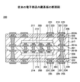
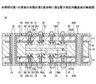
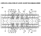
図1は、従来の電子部品内蔵基板の断面図である。 FIG. 1 is a cross-sectional view of a conventional electronic component built-in substrate.
図1を参照するに、従来の電子部品内蔵基板200は、コア基板201と、貫通ビア202,203と、電子部品実装用パッド205,208と、パッド206,209,221,231と、電子部品211,214と、アンダーフィル樹脂212,215と、樹脂層217,222,228,232と、ビア218,229,223,234と、外部接続用パッド225,235とを有する。
Referring to FIG. 1, a conventional electronic component built-in
貫通ビア202は、コア基板201を貫通するように形成されている。貫通ビア202の上端は、コア基板201の上面201Aに形成された電子部品実装用パッド205と接続されており、貫通ビア202の下端は、コア基板201の下面201Bに形成された電子部品実装用パッド208と接続されている。
The
貫通ビア203は、コア基板201を貫通するように形成されている。貫通ビア203の上端は、コア基板201の上面201Aに形成されたパッド206と接続されており、貫通ビア203の下端は、コア基板201の下面201Bに形成されたパッド209と接続されている。
The
電子部品実装用パッド205は、コア基板201の上面201Aに設けられており、貫通ビア202と接続されている。電子部品実装用パッド208は、コア基板201の下面201Bに設けられており、貫通ビア202と接続されている。電子部品実装用パッド205,208は、貫通ビア202を介して、電気的に接続されている。
The electronic
パッド206は、コア基板201の上面201Aに形成されている。パッド209は、コア基板201の下面201Bに形成されている。パッド209は、貫通ビア203を介して、パッド206と電気的に接続されている。
The
電子部品211は、電子部品実装用パッド205に対して表面実装されている。アンダーフィル樹脂212は、電子部品211と電子部品実装用パッド205が形成されたコア基板201との隙間を充填するように配設されている。
The
電子部品214は、電子部品実装用パッド208に対して表面実装されている。アンダーフィル樹脂215は、電子部品214と電子部品実装用パッド208が形成されたコア基板201との隙間を充填するように配設されている。
The
樹脂層217は、電子部品211を覆うように、コア基板201の上面201Aに設けられている。ビア218は、パッド206上に配置された部分の樹脂層217を貫通するように設けられている。ビア218の下端は、パッド206と接続されている。パッド221は、樹脂層217の上面217Aに設けられており、ビア218の上端と接続されている。
The
樹脂層222は、パッド221を覆うように、樹脂層217の上面217Aに設けられている。ビア223は、パッド221上に配置された部分の樹脂層222を貫通するように設けられている。ビア223の下端は、パッド221と接続されている。外部接続用パッド225は、樹脂層222の上面222Aに設けられており、ビア223の上端と接続されている。
The
樹脂層228は、電子部品214を覆うように、コア基板201の下面201Bに設けられている。ビア229は、パッド209と対向する部分の樹脂層228を貫通するように設けられている。ビア229の上端は、パッド209と接続されている。パッド231は、樹脂層228の下面228Aに設けられており、ビア229の下端と接続されている。
The
樹脂層232は、パッド231を覆うように、樹脂層228の下面228Aに設けられている。ビア234は、パッド231と対向する部分の樹脂層232を貫通するように設けられている。ビア234の上端は、パッド231と接続されている。外部接続用パッド235は、樹脂層232の下面232Aに設けられており、ビア234の下端と接続されている。
The
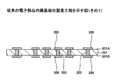
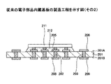
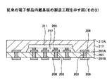
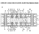
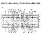
図2〜図7は、従来の電子部品内蔵基板の製造工程を示す図である。図2〜図7において、従来の電子部品内蔵基板200と同一構成部分には同一符号を付す。
2 to 7 are views showing a manufacturing process of a conventional electronic component built-in substrate. 2-7, the same code | symbol is attached | subjected to the same component as the conventional electronic component built-in
図2〜図7を参照して、従来の電子部品内蔵基板200の製造方法について説明する。始めに、図2に示す工程では、周知の手法により、コア基板201に、貫通ビア202,203、電子部品実装用パッド205,208、及びパッド206,209を形成する。
With reference to FIGS. 2 to 7, a conventional method for manufacturing the electronic component built-in
次いで、図3に示す工程では、電子部品実装用パッド205に電子部品211を表面実装し、その後、コア基板201と電子部品211との隙間を充填するアンダーフィル樹脂212を形成する。
Next, in the step shown in FIG. 3, the
次いで、図4に示す工程では、図3に示す構造体の上面側に、電子部品211を覆う樹脂層217を形成する。具体的には、樹脂層217は、図3に示す構造体の上面側に半硬化状態とされた樹脂フィルムを貼り付け、その後、図4に示す構造体全体を加熱して、樹脂フィルムを完全に硬化させることで形成する。
Next, in a step shown in FIG. 4, a
次いで、図5に示す工程では、電子部品実装用パッド208に電子部品214を表面実装し、その後、コア基板201と電子部品214との隙間を充填するアンダーフィル樹脂215を形成する。
Next, in the step shown in FIG. 5, the
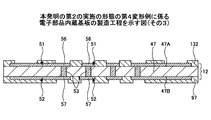
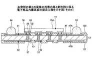
次いで、図6に示す工程では、図5に示す構造体の下面側に、電子部品214を覆う樹脂層228を形成する。具体的には、樹脂層228は、図5に示す構造体の下面側に半硬化状態とされた樹脂フィルムを貼り付け、その後、図5に示す構造体全体を加熱して、樹脂フィルムを完全に硬化させることで形成する。
Next, in a step shown in FIG. 6, a
次いで、図7に示す工程では、ビルドアップ法により、パッド221,231、樹脂層217,222,228,232、ビア218,229,223,234、及び外部接続用パッド225,235を形成する。これにより、従来の電子部品内蔵基板200が製造される(例えば、特許文献1参照。)。
しかしながら、従来の電子部品内蔵基板200では、電子部品内蔵基板200の中心部に、電子部品211,214を実装するためのコア基板201が必要となるため、電子部品内蔵基板200の厚さ方向のサイズを小型化することが困難であるという問題があった。
However, in the conventional electronic component built-in
また、従来の電子部品内蔵基板200の製造方法では、図4に示す工程において、コア基板201の上面201A側に形成された構造体と、コア基板201の下面201B側に形成された構造体とが非対称の状態で、図4に示す構造体全体を加熱して、半硬化状態とされた樹脂フィルムを完全に硬化させることにより、樹脂層217を形成していた。そのため、図4に示す構造体に反りが発生し、この反りが電子部品内蔵基板200に残ってしまうという問題があった。
In the conventional method for manufacturing the electronic component built-in
そこで本発明は、上述した問題点に鑑みなされたものであり、電子部品内蔵基板の厚さ方向のサイズを小型化することのできる電子部品内蔵基板、及び電子部品内蔵基板の厚さ方向のサイズを小型化することができると共に、電子部品内蔵基板の製造時における反りの発生を防止することのできる電子部品内蔵基板の製造方法を提供することを目的とする。 Therefore, the present invention has been made in view of the above-described problems, and can be reduced in size in the thickness direction of the electronic component built-in substrate, and the size in the thickness direction of the electronic component built-in substrate. It is an object of the present invention to provide a method for manufacturing an electronic component built-in substrate capable of reducing the size of the electronic component built-in substrate and preventing warpage during the manufacture of the electronic component built-in substrate.
本発明の一観点によれば、第1の配線基板本体及び該第1の配線基板本体の第1の面に設けられた第1の配線パターンを有する第1の配線基板と、前記第1の配線パターンに表面実装された第1の電子部品と、第2の配線基板本体及び該第2の配線基板本体の第1の面に設けられた第2の配線パターンを有し、前記第1の配線基板本体の第1の面と前記第2の配線基板本体の第1の面とが対向するように、前記第1の配線基板の下方に配置された第2の配線基板と、前記第2の配線パターンに表面実装されると共に、前記第1の電子部品と対向するように配置された第2の電子部品と、前記第1の電子部品が接続された前記第1の配線基板と、前記第2の電子部品が接続された前記第2の配線基板との間を封止する樹脂部材と、を有することを特徴とする電子部品内蔵基板が提供される。 According to one aspect of the present invention, a first wiring board having a first wiring board main body and a first wiring pattern provided on a first surface of the first wiring board main body, and the first wiring board A first electronic component that is surface-mounted on the wiring pattern, a second wiring board body, and a second wiring pattern provided on a first surface of the second wiring board body, A second wiring board disposed below the first wiring board such that the first surface of the wiring board body and the first surface of the second wiring board body face each other; and A second electronic component that is surface-mounted on the wiring pattern and disposed to face the first electronic component, the first wiring substrate to which the first electronic component is connected, and And a resin member that seals between the second wiring board to which the second electronic component is connected. Electronic-part built-in substrate according to claim is provided.
本発明によれば、第1の配線基板本体及び第1の配線基板本体の第1の面に設けられた第1の配線パターンを有する第1の配線基板と、第1の配線パターンに表面実装された第1の電子部品と、第2の配線基板本体及び第2の配線基板本体の第1の面に設けられた第2の配線パターンを有し、第1の配線基板本体の第1の面と第2の配線基板本体の第1の面とが対向するように、第1の配線基板の下方に配置された第2の配線基板と、第2の配線パターンに表面実装されると共に、第1の電子部品と対向するように配置された第2の電子部品と、第1の電子部品が接続された第1の配線基板と、第2の電子部品が接続された第2の配線基板との間を封止する樹脂部材と、を有することにより、コア基板の両面に実装された電子部品を内蔵する従来の電子部品内蔵基板と比較して、電子部品内蔵基板の厚さ方向のサイズを小型化することができる。 According to the present invention, a first wiring board having a first wiring board body and a first wiring pattern provided on a first surface of the first wiring board body, and surface mounting on the first wiring pattern. The first wiring board main body and the second wiring pattern provided on the first surface of the second wiring board main body and the first wiring board main body. The surface is mounted on a second wiring board disposed below the first wiring board and the second wiring pattern so that the first face of the second wiring board main body faces the first wiring board, A second electronic component disposed so as to face the first electronic component; a first wiring substrate to which the first electronic component is connected; and a second wiring substrate to which the second electronic component is connected Electronic components mounted on both sides of the core substrate Compared to electronic-part built-in substrate of years, the electronic component-embedded board in the thickness direction size can be miniaturized.
本発明の他の観点によれば、第1の配線基板本体及び該第1の配線基板本体の第1の面に設けられた第1の配線パターンを備えた第1の配線基板を形成する第1の配線基板形成工程と、前記第1の配線パターンに第1の電子部品を表面実装する第1の電子部品実装工程と、第2の配線基板本体及び該第2の配線基板本体の第1の面に設けられた第2の配線パターンを備えた第2の配線基板を形成する第2の配線基板形成工程と、前記第2の配線パターンに第2の電子部品を表面実装する第2の電子部品実装工程と、板状とされ、前記第1及び第2の電子部品が収容される第1の貫通部を有すると共に、半硬化状態とされた樹脂部材を形成する樹脂部材形成工程と、前記第1の貫通部に、前記第1の配線基板に表面実装された前記第1の電子部品と前記第2の配線基板に表面実装された前記第2の電子部品とを挿入して、前記第1の電子部品及び前記第2の電子部品を対向配置させることにより、前記第1の電子部品が表面実装された第1の配線基板と、前記半硬化状態とされた樹脂部材と、前記第2の電子部品が表面実装された第2の配線基板とが積層された積層体を形成する積層体形成工程と、前記積層体を加熱した状態でプレスして、前記半硬化状態とされた樹脂部材を完全に硬化させることにより、前記第1の電子部品が表面実装された前記第1の配線基板と、前記第2の電子部品が表面実装された前記第2の配線基板との間を封止する封止工程と、を含むことを特徴とする電子部品内蔵基板の製造方法が提供される。 According to another aspect of the present invention, a first wiring board is provided that includes a first wiring board body and a first wiring pattern provided on a first surface of the first wiring board body. A first wiring board forming step, a first electronic component mounting step for surface-mounting a first electronic component on the first wiring pattern, a second wiring board body, and a first of the second wiring board body. A second wiring board forming step of forming a second wiring board provided with a second wiring pattern provided on the surface, and a second electronic component surface-mounted on the second wiring pattern. An electronic component mounting step, a resin member forming step for forming a resin member that is plate-shaped and has a first through portion in which the first and second electronic components are accommodated, and a semi-cured state, The first electronic part surface-mounted on the first wiring board in the first penetration part And the second electronic component that is surface-mounted on the second wiring board, and the first electronic component and the second electronic component are arranged to face each other, thereby the first electronic component Is a laminate that forms a laminate in which a first wiring board having a surface mounted thereon, a semi-cured resin member, and a second wiring board having a surface mounted on the second electronic component are stacked. The first wiring in which the first electronic component is surface-mounted by pressing the laminated body in a heated state to completely cure the semi-cured resin member And a sealing step for sealing between the substrate and the second wiring substrate on which the second electronic component is surface-mounted. A method for manufacturing an electronic component-embedded substrate is provided. .
本発明によれば、第1の配線基板本体及び第1の配線基板本体の第1の面に設けられた第1の配線パターンを備えた第1の配線基板を形成し、第1の配線パターンに第1の電子部品を表面実装し、第2の配線基板本体及び第2の配線基板本体の第1の面に設けられた第2の配線パターンを備えた第2の配線基板を形成し、第2の配線パターンに第2の電子部品を表面実装し、板状とされ、第1及び第2の電子部品が収容される第1の貫通部を有すると共に、半硬化状態とされた樹脂部材を形成し、第1の貫通部に、第1の配線基板に表面実装された第1の電子部品と第2の配線基板に表面実装された第2の電子部品とを挿入して、第1の電子部品及び第2の電子部品を対向配置させることにより、第1の電子部品が表面実装された第1の配線基板と、半硬化状態とされた樹脂部材と、第2の電子部品が表面実装された第2の配線基板とが積層された積層体を形成し、その後、積層体を加熱した状態でプレスして、半硬化状態とされた樹脂部材を完全に硬化させることで第1の電子部品が表面実装された第1の配線基板と、第2の電子部品が表面実装された第2の配線基板との間を封止することにより、コア基板の両面に実装された電子部品を内蔵する従来の電子部品内蔵基板と比較して、電子部品内蔵基板の厚さ方向のサイズを小型化することができる。 According to the present invention, a first wiring board having a first wiring board body and a first wiring pattern provided on a first surface of the first wiring board body is formed, and the first wiring pattern is formed. Surface-mounting the first electronic component to form a second wiring board having a second wiring board body and a second wiring pattern provided on the first surface of the second wiring board body, The second electronic component is surface-mounted on the second wiring pattern, is in the form of a plate, has a first through portion in which the first and second electronic components are accommodated, and is a semi-cured resin member The first electronic component surface-mounted on the first wiring board and the second electronic component surface-mounted on the second wiring board are inserted into the first penetrating portion, and the first through-hole is inserted. The first wiring on which the first electronic component is surface-mounted by arranging the electronic component and the second electronic component to face each other A laminated body is formed by laminating a plate, a resin member in a semi-cured state, and a second wiring substrate on which a second electronic component is surface-mounted, and then the laminated body is pressed in a heated state. A first wiring board on which the first electronic component is surface-mounted by completely curing the semi-cured resin member, and a second wiring board on which the second electronic component is surface-mounted. By sealing the gap, the size in the thickness direction of the electronic component built-in substrate can be reduced as compared with the conventional electronic component built-in substrate incorporating the electronic components mounted on both surfaces of the core substrate. .
また、半硬化状態とされた樹脂部材の面に第1の電子部品が表面実装された第1の配線基板を配置し、半硬化状態とされた樹脂部材の面に第2の電子部品が実装された第2の配線基板を配置した状態(半硬化状態とされた樹脂部材の両面に略同様な構成とされた構造体が配置された状態)で、加熱により半硬化状態の樹脂部材を完全に硬化させて、第1の電子部品が表面実装された第1の配線基板と第2の電子部品が表面実装された第2の配線基板との間を封止することで、電子部品内蔵基板に反りが発生することを防止できる。 Also, the first wiring board on which the first electronic component is surface-mounted is disposed on the surface of the resin member that is semi-cured, and the second electronic component is mounted on the surface of the resin member that is semi-cured. In a state where the second wiring board is disposed (a structure having a substantially similar structure is disposed on both surfaces of the semi-cured resin member), the semi-cured resin member is completely removed by heating. The electronic component-embedded substrate is sealed by sealing between the first wiring substrate on which the first electronic component is surface-mounted and the second wiring substrate on which the second electronic component is surface-mounted. It is possible to prevent warping from occurring.
本発明によれば、電子部品内蔵基板の厚さ方向のサイズを小型化することができると共に、電子部品内蔵基板の製造時に反りが発生することを防止できる。 ADVANTAGE OF THE INVENTION According to this invention, while being able to reduce the size of the thickness direction of a board | substrate with a built-in electronic component, it can prevent generating a curvature at the time of manufacture of a board | substrate with a built-in electronic component.
次に、図面に基づいて本発明の実施の形態について説明する。 Next, embodiments of the present invention will be described with reference to the drawings.
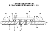
(第1の実施の形態)
図8は、本発明の第1の実施の形態に係る電子部品内蔵基板の断面図である。
(First embodiment)
FIG. 8 is a cross-sectional view of the electronic component built-in substrate according to the first embodiment of the present invention.
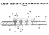
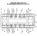
図8を参照するに、第1の実施の形態の電子部品内蔵基板10は、第1の配線基板11と、第2の配線基板12と、第1の電子部品14と、第2の電子部品15と、樹脂部材16と、貫通孔18と、貫通電極19と、ソルダーレジスト層22と、第1の外部接続端子24と、第2の外部接続端子25とを有する。
Referring to FIG. 8, the electronic component built-in
第1の配線基板11は、第1の配線基板本体である配線基板本体35と、第1の配線パターンである配線パターン37と、第3の配線パターンである配線パターン38と、配線パターン39とを有する。配線基板本体35としては、例えば、樹脂層、コアレス基板(積層された複数の樹脂層、及び複数の樹脂層に設けられた配線パターンを有する多層配線構造体)、コア付きビルドアップ基板(コア基板に複数の樹脂層及び配線パターンが形成された基板)等を用いることができる。
The
配線パターン37は、配線基板本体35の面35A(第1の面)に設けられている。配線パターン37は、パッド部42を有する。パッド部42は、配線パターン39の一方の端部、電子部品14と電気的に接続されたバンプ28、及び貫通電極19と電気的に接続されている。これにより、配線パターン37は、貫通電極19と電子部品14とを電気的に接続している。配線パターン37の材料としては、例えば、Cuを用いることができる。
The
配線パターン38は、配線基板本体35の面35Aとは反対側に位置する配線基板本体35の面35B(第2の面)に設けられている。配線パターン38は、パッド部44を有する。パッド部44は、配線パターン39の他方の端部及び貫通電極19と接続されると共に、第1の外部接続端子24が配設されている。配線パターン38の材料としては、例えば、Cuを用いることができる。
The
配線パターン39は、配線基板本体35を貫通するように設けられている。配線パターン39の一方の端部は、パッド部42と接続されており、配線パターン39の他方の端部は、パッド部44と接続されている。これにより、配線パターン39は、配線パターン37と配線パターン38とを電気的に接続している。配線パターン39としては、例えば、ビア、複数のビア及び配線等を用いることができる。配線パターン39の材料としては、例えば、Cuを用いることができる。
The
第2の配線基板12は、第2の配線基板本体である配線基板本体47と、第2の配線パターンである配線パターン51と、第4の配線パターンである配線パターン52と、配線パターン53とを有しており、配線基板本体35の面35Aと配線基板本体47の面47A(第1の面)とが対向するように、第1の配線基板11の下方に配置されている。
The
配線基板本体47としては、例えば、樹脂層、コアレス基板(積層された複数の樹脂層、及び複数の樹脂層に設けられた配線パターンを有する多層配線構造体)、コア付きビルドアップ基板(コア基板に複数の樹脂層及び配線パターンが形成された基板)等を用いることができる。
As the wiring board
配線パターン51は、配線基板本体47の面47A(第1の面)に設けられている。配線パターン51は、パッド部56を有する。パッド部56は、配線パターン53の一方の端部、電子部品15と電気的に接続されたバンプ29、及び貫通電極19と電気的に接続されている。これにより、配線パターン51は、貫通電極19と電子部品15とを電気的に接続している。配線パターン51の材料としては、例えば、Cuを用いることができる。
The
配線パターン52は、配線基板本体47の面47Aとは反対側に位置する配線基板本体47の面47B(第2の面)に設けられている。配線パターン52は、パッド部57を有する。パッド部57は、配線パターン53の他方の端部及び貫通電極19と接続されると共に、第1の外部接続端子24が配設されている。配線パターン52の材料としては、例えば、Cuを用いることができる。
The
配線パターン53は、配線基板本体47を貫通するように設けられている。配線パターン53の一方の端部は、パッド部56と接続されており、配線パターン53の他方の端部は、パッド部57と接続されている。これにより、配線パターン53は、配線パターン51と配線パターン52とを電気的に接続している。配線パターン53としては、例えば、ビア、複数のビア及び配線等を用いることができる。配線パターン53の材料としては、例えば、Cuを用いることができる。
The
第1の電子部品14は、配線パターン37を構成するパッド部42に対して表面実装されている。具体的には、第1の電子部品14は、電極パッド61(第1の電子部品14の構成要素の1つ)に設けられたバンプ28(例えば、Auバンプ)を介して、パッド部42と電気的に接続されている。バンプ28は、はんだ31によりパッド部42に固定されている。第1の電子部品14は、第1の配線基板11と第2の配線基板12との間に配置されている。第1の電子部品14は、樹脂部材16により封止されている。また、第1の電子部品14と第1の配線基板11との隙間には、樹脂部材16が充填されている。第1の電子部品14としては、例えば、半導体チップ、チップ抵抗、チップコンデンサ等を用いることができる。
The first
第2の電子部品15は、配線パターン51を構成するパッド部56に対して表面実装されている。具体的には、第2の電子部品15は、電極パッド63(第2の電子部品15の構成要素の1つ)に設けられたバンプ29(例えば、Auバンプ)を介して、パッド部56と電気的に接続されている。バンプ29は、はんだ32によりパッド部56に固定されている。第2の電子部品15の面15A(第1の電子部品14と対向する部分の第2の電子部品15の面)の面積は、第1の電子部品14の面14A(第2の電子部品15と対向する部分の第1の電子部品14の面)の面積と略等しい大きさとされている。
The second
第2の電子部品15は、第1の配線基板11に実装された第1の電子部品14と対向するように、第1の配線基板11と第2の配線基板12との間に配置されている。第2の電子部品15と第1の電子部品14との間には、隙間Aが形成されている。第2の電子部品15は、樹脂部材16により封止されている。また、第2の電子部品15と第2の配線基板12との隙間、及び第1の電子部品14と第2の電子部品15との隙間Aには、樹脂部材16が充填されている。第1の電子部品14と第2の電子部品15との隙間Aは、例えば、10μmとすることができる。第2の電子部品15としては、例えば、半導体チップ、チップ抵抗、チップコンデンサ等を用いることができる。
The second
このように、第1の配線基板11に表面実装された第1の電子部品14と、第2の配線基板12に表面実装された第2の電子部品15とが対向するように、対向配置された第1の配線基板11と第2の配線基板12との間を樹脂部材16で封止することにより、従来、電子部品211,214を表面実装する基板として必要であったコア基板201(図1参照)が不要となるため、電子部品内蔵基板10の厚さ方向のサイズを小型化することができる。
In this way, the first
樹脂部材16は、樹脂が完全に硬化した部材であり、第1の電子部品14が表面実装された第1の配線基板11と、第2の電子部品15が表面実装された第2の配線基板12との間に設けられている。樹脂部材16は、第1の配線基板11と第2の配線基板12との間、第1の電子部品14、及び第2の電子部品15を封止すると共に、第1の電子部品14が表面実装された第1の配線基板11と、第2の電子部品15が表面実装された第2の配線基板12とを一体化するための部材である。樹脂部材16は、第1の電子部品14と第1の配線基板11との隙間、第2の電子部品15と第2の配線基板12との隙間、及び第1の電子部品14と第2の電子部品15との隙間Aを充填している。樹脂部材16の母材としては、例えば、第1及び第2の電子部品14,15の配設領域に対応する部分に第1の貫通部85(図16参照)を有したプリプレグ樹脂を用いることができる。
The
このように、樹脂部材16の母材としてプリプレグ樹脂を用いることにより、電子部品内蔵基板10に反りが発生することを防止できる。樹脂部材16の厚さBは、例えば、300μmとすることができる。
As described above, by using the prepreg resin as the base material of the
樹脂部材16の母材としてプリプレグ樹脂を用いる場合、第1の電子部品14と第1の配線基板11との隙間、第2の電子部品15と第2の配線基板12との隙間、及び第1の電子部品14と第2の電子部品15との隙間Aは、プリプレグ樹脂に含まれる樹脂のみが充填される。
When the prepreg resin is used as the base material of the
このように、第1の電子部品14と第2の電子部品15との隙間Aに樹脂のみを配置することにより、第1の電子部品14と第2の電子部品15との隙間Aを小さく(例えば、10μm)することが可能となるため、電子部品内蔵基板10の厚さ方向のサイズを小型化することができる。
Thus, by arranging only the resin in the gap A between the first
貫通孔18は、第1の配線基板11、第2の配線基板12、及び樹脂部材16を貫通するように形成されている。貫通孔18は、配線パターン37,38,51,52を貫通している。これにより、配線パターン37,51は、貫通孔18から露出されている。貫通孔18は、例えば、NCドリルを用いて形成することができる。
The through
貫通電極19は、貫通孔18の側面を覆うように設けられている。貫通電極19は、配線パターン37,38,51,52と接続されている。貫通電極19は、筒状とされており、内部に中空部を有する。貫通電極19の材料としては、例えば、Cuを用いることができる。貫通電極19は、例えば、めっき法により形成することができる。
The through
ソルダーレジスト層22は、配線基板本体35,47の面35B,47B、パッド部44を除いた部分の配線パターン38、パッド部57を除いた部分の配線パターン52、及び貫通電極19の内壁を覆うように設けられている。ソルダーレジスト層22は、パッド部44を露出する開口部22Aと、パッド部57を露出する開口部22Bとを有する。
The solder resist
第1の外部接続端子24は、開口部22Aから露出された部分のパッド部44に設けられている。第1の外部接続端子24は、例えば、図示していない半導体チップと電気的に接続される端子である。第1の外部接続端子24としては、例えば、はんだバンプを用いることができる。
The first
第2の外部接続端子25は、開口部22Bから露出された部分のパッド部57に設けられている。第2の外部接続端子25は、例えば、マザーボード等の実装基板(図示せず)と電気的に接続される端子である。第2の外部接続端子25としては、例えば、はんだボールを用いることができる。
The second
本実施の形態の電子部品内蔵基板によれば、配線基板本体35及び配線基板本体35の面35Aに設けられた配線パターン37を有する第1の配線基板11と、配線パターン37に表面実装された第1の電子部品14と、配線基板本体47及び配線基板本体47の面47Aに設けられた配線パターン51を有し、配線基板本体35の面35Aと配線基板本体47の面47Aとが対向するように、第1の配線基板11の下方に配置された第2の配線基板12と、配線パターン51に表面実装されると共に、第1の電子部品14と対向するように配置された第2の電子部品15と、第1の電子部品14が表面実装された第1の配線基板11と、第2の電子部品が表面実装された第2の配線基板12との間を封止する樹脂部材16と、を備えることにより、コア基板201の両面201A,201Bに実装された電子部品211,214を内蔵する従来の電子部品内蔵基板200と比較して、電子部品内蔵基板10の厚さ方向のサイズを小型化することができる。
According to the electronic component built-in substrate of the present embodiment, the
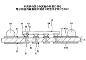
図9は、本発明の第1の実施の形態の第1変形例に係る電子部品内蔵基板の断面図である。図9において、第1の実施の形態の電子部品内蔵基板10と同一構成部分には同一符号を付す。
FIG. 9 is a cross-sectional view of an electronic component built-in substrate according to a first modification of the first embodiment of the present invention. In FIG. 9, the same components as those of the electronic component built-in
図9を参照するに、第1の実施の形態の第1変形例に係る電子部品内蔵基板70は、第1の実施の形態の電子部品内蔵基板10の構成に、さらに第1の電子部品14と第1の配線基板11との隙間を充填する第1のアンダーフィル樹脂71と、第2の電子部品15と第2の配線基板12との隙間を充填する第2のアンダーフィル樹脂72とを設けた以外は、電子部品内蔵基板10と同様に構成される。
Referring to FIG. 9, an electronic component built-in
このように、第1の電子部品14と第1の配線基板11との隙間を充填する第1のアンダーフィル樹脂71と、第2の電子部品15と第2の配線基板12との隙間を充填する第2のアンダーフィル樹脂72とを設けることにより、第1の電子部品14と第1の配線基板11との電気的接続信頼性、及び第2の電子部品15と第2の配線基板12との電気的接続信頼性を向上させることができる。
In this manner, the
また、上記構成とされた第1の実施の形態の第1変形例に係る電子部品内蔵基板70は、第1の実施の形態の電子部品内蔵基板10と同様な効果を得ることができる。
Moreover, the electronic component built-in
図10は、本発明の第1の実施の形態の第2変形例に係る電子部品内蔵基板の断面図である。図10において、第1の実施の形態の電子部品内蔵基板10と同一構成部分には同一符号を付す。
FIG. 10 is a cross-sectional view of an electronic component built-in substrate according to a second modification of the first embodiment of the present invention. In FIG. 10, the same components as those of the electronic component built-in
図9を参照するに、第1の実施の形態の第2変形例に係る電子部品内蔵基板75は、第1の実施の形態の電子部品内蔵基板10に設けられた第2の電子部品15の代わりに、第1の電子部品14の面14Aと対向する面76Aの面積が第1の電子部品14の面14Aの面積よりも小さい第2の電子部品76を複数設けた以外は、電子部品内蔵基板10と同様に構成される。
Referring to FIG. 9, the electronic component built-in
第2の電子部品76は、面76Aの面積が第2の電子部品15の面15Aの面積よりも小さい以外は、第2の電子部品15と同様に構成される。複数の第2の電子部品76は、面76Aが第1の電子部品14の面14Aと対向するように、配線パターン51のパッド部56に表面実装(第2の電子部品76に設けられた電極パッド63に設けられたバンプ29を介して接続)されている。複数の第2の電子部品76の面76Aの面積の合計は、第1の電子部品14の面14Aの面積と略等しくなるように構成されている。
The second
上記構成とされた第1の実施の形態の第2変形例に係る電子部品内蔵基板75は、第1の実施の形態の電子部品内蔵基板10と同様な効果を得ることができる。なお、第1の実施の形態の第2変形例に係る電子部品内蔵基板75において、第1の電子部品14と第1の配線基板11との間に図10に示す第1のアンダーフィル樹脂71を設けてもよいし、複数の第2の電子部品76と第2の配線基板12との間に図10に示す第2のアンダーフィル樹脂72を設けてもよい。
The electronic component built-in
図11は、本発明の第1の実施の形態の第3変形例に係る電子部品内蔵基板の断面図である。図11において、第1の実施の形態の電子部品内蔵基板10と同一構成部分には同一符号を付す。
FIG. 11 is a cross-sectional view of an electronic component built-in substrate according to a third modification of the first embodiment of the present invention. In FIG. 11, the same components as those of the electronic component built-in
図11を参照するに、第1の実施の形態の第3変形例に係る電子部品内蔵基板80は、第1の実施の形態の電子部品内蔵基板10に設けられた第1の電子部品14の代わりに、第2の電子部品15の面15Aと対向する面81Aの面積が第2の電子部品15の面15Aの面積よりも小さい第1の電子部品81を複数設けた以外は、電子部品内蔵基板10と同様に構成される。
Referring to FIG. 11, the electronic component built-in
第1の電子部品81は、面81Aの面積が第1の電子部品14の面14Aの面積よりも小さい以外は、第1の電子部品14と同様に構成される。複数の第1の電子部品81は、面81Aが第2の電子部品15の面15Aと対向するように、配線パターン37のパッド部42に表面実装(第1の電子部品81に設けられた電極パッド61に設けられたバンプ28を介して接続)されている。複数の第1の電子部品81の面81Aの面積の合計は、第2の電子部品15の面15Aの面積と略等しくなるように構成されている。
The first
上記構成とされた第1の実施の形態の第3変形例に係る電子部品内蔵基板80は、第1の実施の形態の電子部品内蔵基板10と同様な効果を得ることができる。なお、第1の実施の形態の第3変形例に係る電子部品内蔵基板80において、複数の第1の電子部品81と第1の配線基板11との間に図10に示す第1のアンダーフィル樹脂71を設けてもよいし、第2の電子部品15と第2の配線基板12との間に図10に示す第2のアンダーフィル樹脂72を設けてもよい。
The electronic component built-in
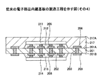
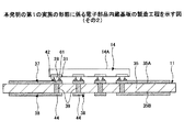
図12〜図22は、本発明の第1の実施の形態に係る電子部品内蔵基板の製造工程を示す図である。図12〜図22において、第1の実施の形態の電子部品内蔵基板10と同一構成部分には同一符号を付す。
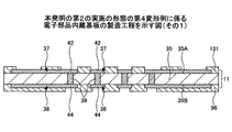
12 to 22 are views showing a manufacturing process of the electronic component built-in substrate according to the first embodiment of the present invention. 12 to 22, the same components as those of the electronic component built-in
図12〜図22を参照して、第1の実施の形態の電子部品内蔵基板10の製造方法について説明する。始めに、図12に示す工程では、周知の手法(例えば、ビルドアップ法)により、第1の配線基板本体である配線基板本体35と、第1の配線パターンである配線パターン37と、第3の配線パターンである配線パターン38と、配線パターン39とを有した第1の配線基板11を形成する(第1の配線基板形成工程)。配線基板本体35としては、例えば、樹脂層、コアレス基板(積層された複数の樹脂層、及び複数の樹脂層に設けられた配線パターンを有する多層配線構造体)、コア付きビルドアップ基板(コア基板に複数の樹脂層及び配線パターンが形成された基板)等を用いることができる。
With reference to FIGS. 12-22, the manufacturing method of the electronic component built-in board |
次いで、図13に示す工程では、パッド部42に第1の電子部品14を表面実装する(第1の電子部品実装工程)。具体的には、パッド部42上に溶融させたはんだ31を準備し、溶融させたはんだ31に第1の電子部品14の電極パッド61に設けられたバンプ28を押し当てることで、パッド部42上にバンプ28を固定する。
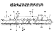
Next, in the step shown in FIG. 13, the first
次いで、図14に示す工程では、周知の手法(例えば、ビルドアップ法)により、第2の配線基板本体である配線基板本体47と、第2の配線パターンである配線パターン51と、第4の配線パターンである配線パターン52と、配線パターン53とを有した第2の配線基板12を形成する(第2の配線基板形成工程)。配線基板本体47としては、例えば、樹脂層、コアレス基板(積層された複数の樹脂層、及び複数の樹脂層に設けられた配線パターンを有する多層配線構造体)、コア付きビルドアップ基板(コア基板に複数の樹脂層及び配線パターンが形成された基板)等を用いることができる。
Next, in the process shown in FIG. 14, the
次いで、図15に示す工程では、パッド部56に第2の電子部品15を表面実装する(第2の電子部品実装工程)。具体的には、パッド部56上に溶融させたはんだ32を準備し、溶融させたはんだ32に第2の電子部品15の電極パッド63に設けられたバンプ29を押し当てることで、パッド部56上にバンプ29を固定する。
Next, in the step shown in FIG. 15, the second
次いで、図16に示す工程では、板状とされ、第1及び第2の電子部品14,15が収容される第1の貫通部85を有すると共に、半硬化状態とされた樹脂部材16を形成する(樹脂部材形成工程)。樹脂部材16の母材としては、例えば、半硬化状態とされたプリプレグ樹脂(具体的には、例えば、ガラス繊維に樹脂を含浸させた絶縁部材)を用いることができる。第1の貫通部85は、例えば、打ち抜き加工により形成することができる。半硬化状態とされた樹脂部材16は、図8に示す完全に硬化した樹脂部材16の厚さBよりも厚い。半硬化状態とされた樹脂部材16の厚さCは、例えば、600μmとすることができる。
Next, in the step shown in FIG. 16, the
次いで、図17に示す工程では、半硬化状態とされた樹脂部材16の上面16A側から第1の貫通部85に、第1の配線基板11に表面実装された第1の電子部品14を挿入し、半硬化状態とされた樹脂部材16の下面16B側から第1の貫通部85に、第2の配線基板12に表面実装された第2の電子部品15を挿入して、第1の電子部品14と第2の電子部品15とを対向配置させることにより、第1の電子部品14が表面実装された第1の配線基板11と、半硬化状態とされた樹脂部材16と、第2の電子部品15が表面実装された第2の配線基板12とが積層された積層体87を形成する(積層体形成工程)。
Next, in the step shown in FIG. 17, the first
このとき、第1の配線基板11は、樹脂部材16の上面16Aと接触し、第2の配線基板12は、樹脂部材16の下面16Bと接触する。また、第1の貫通部85に挿入された第1の電子部品14と、第1の貫通部85に挿入された第2の電子部品15との間には、図8に示す隙間Aよりも大きな隙間が形成されている。
At this time, the
次いで、図18に示す工程では、積層体を加熱した状態でプレスして、図17に示す半硬化状態とされた樹脂部材16を完全に硬化させて、完全に硬化した樹脂部材16により、第1の電子部品14が表面実装された第1の配線基板11と、第2の電子部品15が表面実装された第2の配線基板12との間を封止する(封止工程)。
Next, in the step shown in FIG. 18, the laminate is pressed in a heated state to completely cure the
半硬化状態の樹脂部材16の母材がプリプレグ樹脂の場合、上記封止工程において、第1の電子部品14と第1の配線基板11との隙間、第2の電子部品15と第2の配線基板12との隙間、及び第1の電子部品14と第2の電子部品15と隙間Aに、プリプレグ樹脂を構成する樹脂のみが充填される。
When the base material of the
このように、半硬化状態とされた樹脂部材16の第1の貫通部85に、第1の配線基板11に表面実装された第1の電子部品14と第2の配線基板12に表面実装された第2の電子部品15とを挿入して、第1の電子部品14と第2の電子部品15とを対向配置させることにより、第1の電子部品14が表面実装された第1の配線基板11と、半硬化状態とされた樹脂部材16と、第2の電子部品15が表面実装された第2の配線基板12とが積層された積層体87を形成し、その後、積層体87を加熱した状態でプレスして、半硬化状態とされた樹脂部材16を完全に硬化させて、第1の電子部品14が表面実装された第1の配線基板11と、第2の電子部品15が表面実装された第2の配線基板12との間を封止することにより、コア基板201の両面201A,201Bに実装された電子部品211,214を内蔵する従来の電子部品内蔵基板200と比較して、電子部品内蔵基板10の厚さ方向のサイズを小型化することができる。
In this way, the first
また、半硬化状態とされた樹脂部材16の面16Aに第1の電子部品14が表面実装された第1の配線基板11を配置し、半硬化状態とされた樹脂部材16の面16Bに第2の電子部品15が実装された第2の配線基板12を配置した状態(半硬化状態とされた樹脂部材16の両面16A,16Bに略同様な構成とされた構造体が配置された状態)で、加熱により半硬化状態の樹脂部材16を完全に硬化させて、第1の電子部品14が表面実装された第1の配線基板11と第2の電子部品15が表面実装された第2の配線基板12との間を封止することで、図18に示す構造体(製造途中の電子部品内蔵基板10)に反りが発生することがなくなるため、電子部品内蔵基板10に反りが発生することを防止できる。
Further, the
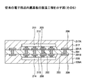
次いで、図19に示す工程では、第1の配線基板11、樹脂部材16、及び第2の配線基板12を貫通する貫通孔18を形成する。貫通孔18は、例えば、NCドリルにより形成することができる。
Next, in a step shown in FIG. 19, a through
次いで、図20に示す工程では、めっき法により、貫通孔18の側面に貫通電極19を形成する。このとき、貫通電極19に中空部が形成される。言い換えれば、筒状とされた貫通電極19が形成される。
Next, in the step shown in FIG. 20, the through
次いで、図21に示す工程では、配線基板本体35,47の面35B,47B、パッド部44を除いた部分の配線パターン38、パッド部57を除いた部分の配線パターン52、及び貫通電極19の内壁を覆うと共に、パッド部44を露出する開口部22Aと、パッド部57を露出する開口部22Bとを有したソルダーレジスト層22を形成する。
Next, in the step shown in FIG. 21, the
次いで、図22に示す工程では、開口部22Aから露出された部分のパッド部44に第1の外部接続端子24を形成し、開口部22Bから露出された部分のパッド部57に第2の外部接続端子25を形成する。これにより、第1の実施の形態の電子部品内蔵基板10が製造される。第1の外部接続端子24としては、例えば、はんだバンプを用いることができる。また、第2の外部接続端子25としては、例えば、はんだボールを用いることができる。
Next, in the process shown in FIG. 22, the first
本実施の形態の電子部品内蔵基板によれば、配線基板本体35及び配線基板本体35の面35Aに設けられた配線パターン37を備えた第1の配線基板11を形成し、配線パターン37に第1の電子部品14を表面実装し、配線基板本体47及び配線基板本体47の面47Aに設けられた配線パターン51を備えた第2の配線基板12を形成し、配線パターン51に第2の電子部品15を表面実装し、板状とされ、第1及び第2の電子部品14,15が収容される第1の貫通部85を有すると共に、半硬化状態とされた樹脂部材16を形成し、第1の貫通部85に、第1の配線基板11に表面実装された第1の電子部品14と第2の配線基板12に表面実装された第2の電子部品15とを挿入して、第1の電子部品14と第2の電子部品15とを対向配置させることにより、第1の電子部品14が表面実装された第1の配線基板11と、半硬化状態とされた樹脂部材16と、第2の電子部品15が表面実装された第2の配線基板12とが積層された積層体87を形成し、その後、積層体87を加熱した状態でプレスして、半硬化状態とされた樹脂部材16を完全に硬化させて、第1の電子部品14が表面実装された第1の配線基板11と、第2の電子部品15が表面実装された第2の配線基板12との間を封止することにより、コア基板201の両面201A,201Bに実装された電子部品211,214を内蔵する従来の電子部品内蔵基板200と比較して、電子部品内蔵基板10の厚さ方向のサイズを小型化することができる。
According to the electronic component built-in substrate of the present embodiment, the
また、半硬化状態とされた樹脂部材16の面16Aに第1の電子部品14が表面実装された第1の配線基板11を配置し、半硬化状態とされた樹脂部材16の面16Bに第2の電子部品15が実装された第2の配線基板12を配置した状態(半硬化状態とされた樹脂部材16の両面16A,16Bに略同様な構成とされた構造体が配置された状態)で、加熱により半硬化状態の樹脂部材16を完全に硬化させて、第1の電子部品14が表面実装された第1の配線基板11と第2の電子部品15が表面実装された第2の配線基板12との間を封止することで、図18に示す構造体(製造途中の電子部品内蔵基板10)に反りが発生することがなくなるため、電子部品内蔵基板10に反りが発生することを防止できる。
Further, the
なお、本実施の形態の第1変形例の電子部品内蔵基板70は、先に説明した図17示す工程(積層体形成工程)の前に、第1のアンダーフィル樹脂71を形成する工程(第1のアンダーフィル樹脂形成工程)と、第2のアンダーフィル樹脂72を形成する工程(第2のアンダーフィル樹脂形成工程)とを設ける以外は、本実施の形態の電子部品内蔵基板10と同様な手法により製造することができる。
Note that the electronic component built-in
このように、積層体形成工程の前に、第1の電子部品14と第1の配線基板11との隙間を充填する第1のアンダーフィル樹脂71を形成する第1のアンダーフィル樹脂形成工程と、第2の電子部品実装工程と積層体形成工程との間に、第2の電子部品15と第2の配線基板12との隙間を充填する第2のアンダーフィル樹脂72を形成する第2のアンダーフィル樹脂形成工程と、を設けることにより、第1の電子部品14と第1の配線基板11との間の電気的接続信頼性、及び第2の電子部品15と第2の配線基板12との間の電気的接続信頼性を向上させることができる。
As described above, the first underfill resin forming step of forming the
また、第1の実施の形態の第2変形例の電子部品内蔵基板75、及び第1の実施の形態の第3変形例の電子部品内蔵基板80は、第1の実施の形態の電子部品内蔵基板10と同様な手法により製造することができる。
Also, the electronic component built-in
また、上記説明した電子部品内蔵基板10,70,75,80では、第1の電子部品14と第2の電子部品15との間に隙間Aを形成した場合を例に挙げて説明したが、第1の電子部品14の面14Aと第2の電子部品15の面15Aとが接触するように、第1及び第2の電子部品14,15を配置してもよい。
Further, in the electronic component built-in
(第2の実施の形態)
図23は、本発明の第2の実施の形態に係る電子部品内蔵基板の断面図である。図23において、第1の実施の形態の電子部品内蔵基板10と同一構成部分には、同一符号を付す。
(Second Embodiment)
FIG. 23 is a cross-sectional view of the electronic component built-in substrate according to the second embodiment of the present invention. In FIG. 23, the same components as those of the electronic component built-in
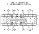
図23を参照するに、第2の実施の形態の電子部品内蔵基板90は、第1の実施の形態の電子部品内蔵基板10に設けられた樹脂部材16、貫通孔18、貫通電極19、及びソルダーレジスト層22の代わりに、樹脂部材92、第1の導電性ボール93、第2の導電性ボール94、及びソルダーレジスト層96,97を設けた以外は、電子部品内蔵基板10と同様に構成される。
Referring to FIG. 23, an electronic component built-in
樹脂部材92は、完全に硬化しており、第1の電子部品14が表面実装された第1の配線基板11と、第2の電子部品15が表面実装された第2の配線基板12との間に設けられている。樹脂部材92は、第1及び第2の電子部品14,15を封止すると共に、第1の電子部品14が表面実装された第1の配線基板11と、第2の電子部品15が表面実装された第2の配線基板12とを一体化するための部材である。樹脂部材92は、第1の電子部品14と第1の配線基板11との隙間、第2の電子部品15と第2の配線基板12との隙間、及び第1の電子部品14と第2の電子部品15との隙間Aを充填している。樹脂部材92の母材としては、例えば、第1及び第2の電子部品14,15の配設領域に対応する部分に第1の貫通部85と、第1及び第2の導電性ボール93,94を収容する第2の貫通部85(図29参照)を有した半硬化状態とされたプリプレグ樹脂を用いることができる。
The
このように、樹脂部材92の母材としてプリプレグ樹脂を用いることにより、電子部品内蔵基板90に反りが発生することを防止できる。樹脂部材92の厚さDは、例えば、300μmとすることができる。
In this way, by using the prepreg resin as the base material of the
第1の導電性ボール93は、配線パターン37に設けられている。第2の導電性ボール94は、第1の導電性ボール93と対向するように、配線パターン51に設けられている。第1の導電性ボール93と対向する部分の第2の導電性ボール94は、第1の導電性ボール93と接触している。これにより、配線パターン37と配線パターン51とは、第1及び第2の導電性ボール93,94を介して、電気的に接続されている。
The first
このように、配線パターン37に設けられた第1の導電性ボール93と、配線パターン51に設けられた第2の導電性ボール94とを接触させることで、配線パターン37と配線パターン51とを電気的に接続することにより、めっき法により形成された貫通電極19を用いて配線パターン37と配線パターン51とを電気的に接続した場合と比較して、電子部品内蔵基板90のコストを低減させることができる。
In this way, by bringing the first
第1及び第2の導電性ボール93,94としては、例えば、はんだボール、CuコアとCuコアを覆うはんだとを備えたCuコアはんだボール等を用いることができる。樹脂部材92の厚さDが300μmの場合、第1及び第2の導電性ボール93,94の直径は、例えば、200μmとすることができる。
As the first and second
ソルダーレジスト層96は、パッド部44を除いた部分の配線パターン38を覆うように、配線基板本体35の面35Bに設けられている。ソルダーレジスト層96は、パッド部44を露出する開口部96Aを有する。
The solder resist
ソルダーレジスト層97は、パッド部57を除いた部分の配線パターン52を覆うように、配線基板本体47の面47Bに設けられている。ソルダーレジスト層97は、パッド部57を露出する開口部97Aを有する。
The solder resist
図24は、本発明の第2の実施の形態の第1変形例に係る電子部品内蔵基板の断面図である。図24において、第2の実施の形態の電子部品内蔵基板90と同一構成部分には、同一符号を付す。
FIG. 24 is a cross-sectional view of an electronic component built-in substrate according to a first modification of the second embodiment of the present invention. In FIG. 24, the same components as those of the electronic component built-in
図24を参照するに、第2の実施の形態の第1変形例に係る電子部品内蔵基板100は、第2の実施の形態の電子部品内蔵基板90の構成に、さらに第1の電子部品14と第1の配線基板11との隙間を充填する第1のアンダーフィル樹脂71と、第2の電子部品15と第2の配線基板12との隙間を充填する第2のアンダーフィル樹脂72とを設けた以外は、電子部品内蔵基板90と同様に構成される。
Referring to FIG. 24, an electronic component built-in
このように、第1の電子部品14と第1の配線基板11との隙間を充填する第1のアンダーフィル樹脂71と、第2の電子部品15と第2の配線基板12との隙間を充填する第2のアンダーフィル樹脂72とを設けることにより、第1の電子部品14と第1の配線基板11との電気的接続信頼性、及び第2の電子部品15と第2の配線基板12との電気的接続信頼性を向上させることができる。
In this manner, the
また、上記構成とされた第2の実施の形態の第1変形例に係る電子部品内蔵基板100は、第2の実施の形態の電子部品内蔵基板90と同様な効果を得ることができる。
Moreover, the electronic component built-in
図25は、本発明の第2の実施の形態の第2変形例に係る電子部品内蔵基板の断面図である。図25において、第2の実施の形態の電子部品内蔵基板90、及び第1の実施の形態の第2変形例に係る電子部品内蔵基板75と同一構成部分には、同一符号を付す。
FIG. 25 is a cross-sectional view of an electronic component built-in substrate according to a second modification of the second embodiment of the present invention. In FIG. 25, the same components as those of the electronic component built-in
図25を参照するに、第2の実施の形態の第2変形例に係る電子部品内蔵基板105は、第2の実施の形態の電子部品内蔵基板90に設けられた第2の電子部品15の代わりに、第1の実施の形態の第2変形例に係る電子部品内蔵基板75に設けられた複数の第2の電子部品76を設けた以外は、電子部品内蔵基板90と同様に構成される。
Referring to FIG. 25, an electronic component built-in
上記構成とされた第2の実施の形態の第2変形例に係る電子部品内蔵基板105は、第2の実施の形態の電子部品内蔵基板90と同様な効果を得ることができる。
The electronic component built-in
図26は、本発明の第2の実施の形態の第3変形例に係る電子部品内蔵基板の断面図である。図26において、第2の実施の形態の電子部品内蔵基板90、及び第1の実施の形態の第3変形例に係る電子部品内蔵基板80と同一構成部分には、同一符号を付す。
FIG. 26 is a cross-sectional view of an electronic component built-in substrate according to a third modification of the second embodiment of the present invention. In FIG. 26, the same components as those of the electronic component built-in
図26を参照するに、第2の実施の形態の第3変形例に係る電子部品内蔵基板110は、第2の実施の形態の電子部品内蔵基板90に設けられた第1の電子部品14の代わりに、第1の実施の形態の第3変形例に係る電子部品内蔵基板80に設けられた複数の第1の電子部品81を設けた以外は、電子部品内蔵基板90と同様に構成される。
Referring to FIG. 26, an electronic component built-in
上記構成とされた第2の実施の形態の第3変形例に係る電子部品内蔵基板110は、第2の実施の形態の電子部品内蔵基板90と同様な効果を得ることができる。
The electronic component built-in
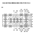
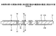
図27〜図32は、本発明の第2の実施の形態に係る電子部品内蔵基板の製造工程を示す図である。図27〜図32において、第2の実施の形態の電子部品内蔵基板90と同一構成部分には同一符号を付す。
27 to 32 are views showing a manufacturing process of the electronic component built-in substrate according to the second embodiment of the present invention. 27 to 32, the same components as those of the electronic component built-in
図27〜32を参照して、第2の実施の形態の電子部品内蔵基板90の製造方法について説明する。始めに、図27に示す工程では、第1の実施の形態で説明した図13に示す構造体に設けられた配線パターン37(具体的には、第1の電子部品14の実装領域以外の部分の配線パターン37)に、第1の導電性ボール93を形成する。第1の導電性ボール93としては、例えば、はんだボール、CuコアとCuコアを覆うはんだとを備えたCuコアはんだボール等を用いることができる。第1の導電性ボール93の直径は、例えば、200μmとすることができる。
With reference to FIGS. 27 to 32, a method of manufacturing the electronic component built-in
次いで、図28に示す工程では、第1の実施の形態で説明した図15に示す構造体に設けられた配線パターン51(具体的には、第2の電子部品15の実装領域以外の部分の配線パターン51)に、第2の導電性ボール94を形成する。第2の導電性ボール94としては、例えば、はんだボール、CuコアとCuコアを覆うはんだとを備えたCuコアはんだボール等を用いることができる。第2の導電性ボール94の直径は、例えば、200μmとすることができる。
Next, in the step shown in FIG. 28, the wiring pattern 51 (specifically, the portion other than the mounting region of the second
次いで、図29に示す工程では、板状とされ、第1及び第2の電子部品14,15が収容される第1の貫通部85と、第1及び第2の導電性ボール93,94を収容する第2の貫通部122とを有すると共に、半硬化状態とされた樹脂部材92を形成する(樹脂部材形成工程)。樹脂部材92の母材としては、例えば、半硬化状態とされたプリプレグ樹脂(具体的には、例えば、ガラス繊維に樹脂を含浸させた絶縁部材)を用いることができる。第1及び第2の貫通部85,122は、例えば、打ち抜き加工により形成することができる。半硬化状態とされた樹脂部材92は、図23に示す完全に硬化した樹脂部材92の厚さDよりも厚い。半硬化状態とされた樹脂部材92の厚さEは、例えば、600μmとすることができる。
Next, in the step shown in FIG. 29, the first through
次いで、図30に示す工程では、半硬化状態とされた樹脂部材92の上面92A側から第1の貫通部85に、第1の配線基板11に表面実装された第1の電子部品14を挿入すると共に、半硬化状態とされた樹脂部材92の上面92A側から第2の貫通部122に第1の配線基板11に設けられた第1の導電性ボール93を挿入する。次いで、半硬化状態とされた樹脂部材92の下面92B側から第1の貫通部85に第2の配線基板12に表面実装された第2の電子部品15を挿入すると共に、半硬化状態とされた樹脂部材92の下面92B側から第2の貫通部122に第2の配線基板12に設けられた第2の導電性ボール94を挿入することで、第2の電子部品15及び第2の導電性ボール94が設けられた第2の配線基板12と、半硬化状態とされた樹脂部材92と、第1の電子部品14及び第1の導電性ボール93が設けられた第1の配線基板11とが積層された積層体125を形成する(積層体形成工程)。
Next, in the step shown in FIG. 30, the first
このとき、第1の配線基板11は、樹脂部材92の上面92Aと接触し、第2の配線基板12は、樹脂部材92の下面92Bと接触する。また、第1の貫通部85に挿入された第1の電子部品14と、第1の貫通部85に挿入された第2の電子部品15との間には、図23に示す隙間Aよりも大きな隙間が形成されている。また、第2の貫通部122に収容された第1及び第2の導電性ボール93,94は、離間した状態で対向配置されている。
At this time, the
次いで、図31に示す工程では、積層体125を加熱した状態でプレスして、第1の導電性ボール93と第2の導電性ボール94とを接触させると共に、図30に示す半硬化状態とされた樹脂部材92を完全に硬化させて、完全に硬化した樹脂部材92により、第1の電子部品14及び第1の導電性ボール93が設けられた第1の配線基板11と、第2の電子部品15及び第2の導電性ボール94が設けられた第2の配線基板12との間を封止する(封止工程)。
Next, in the step shown in FIG. 31, the
半硬化状態の樹脂部材92の母材がプリプレグ樹脂の場合、上記封止工程において、第1の電子部品14と第1の配線基板11との隙間、第2の電子部品15と第2の配線基板12との隙間、及び第1の電子部品14と第2の電子部品15と隙間Aに、プリプレグ樹脂を構成する樹脂のみが充填される。
When the base material of the
このように、半硬化状態とされた樹脂部材92の第1の貫通部85に、第1の配線基板11に表面実装された第1の電子部品14と第2の配線基板12に表面実装された第2の電子部品15とを挿入して、第1の電子部品14と第2の電子部品15とを対向配置させると共に、第1の配線基板11に設けられた第1の導電性ボール93と第2の配線基板12に設けられた第2の導電性ボール94とを挿入して、第1の導電性ボール93と第2の導電性ボール94とを対向配置させることにより、第1の電子部品14及び第1の導電性ボール93が設けられた第1の配線基板11と、半硬化状態とされ、第1及び第2の貫通部85,122を有する樹脂部材92と、第2の電子部品15及び第2の導電性ボール94が設けられた第2の配線基板12とが積層された積層体125を形成し、その後、積層体125を加熱した状態でプレスして、第1の導電性ボール93と第2の導電性ボール94とを接触させると共に、半硬化状態とされた樹脂部材92を完全に硬化させて、第1の電子部品14及び第1の導電性ボール93が設けられた第1の配線基板11と、第2の電子部品15及び第2の導電性ボール94が設けられた第2の配線基板12との間を封止することにより、コア基板201の両面201A,201Bに実装された電子部品211,214を内蔵する従来の電子部品内蔵基板200と比較して、電子部品内蔵基板90の厚さ方向のサイズを小型化することができる。
Thus, the first
また、半硬化状態とされた樹脂部材92の面92Aに第1の電子部品14及び第1の導電性ボール93が設けられた第1の配線基板11を配置し、半硬化状態とされた樹脂部材92の面92Bに第2の電子部品15及び第2の導電性ボール94が設けられた第2の配線基板12を配置した状態(半硬化状態とされた樹脂部材92の両面92A,92Bに略同様な構成とされた構造体が配置された状態)で、加熱により半硬化状態の樹脂部材92を完全に硬化させて、第1の電子部品14及び第1の導電性ボール93が設けられた第1の配線基板11と、第2の電子部品15及び第2の導電性ボール94が設けられた第2の配線基板12との間を封止することで、電子部品内蔵基板90に反りが発生することを防止できる。
In addition, the
さらに、積層体125を加熱した状態でプレスして、第1の配線基板11に設けられた第1の導電性ボール93と、第2の配線基板12に設けられた第2の導電性ボール94とを接触させて、第1の配線基板11と第2の配線基板12とを電気的に接続することにより、めっき法により形成された貫通電極19(図8参照)を介して、第1の配線基板11と第2の配線基板12とを電気的に接続した電子部品内蔵基板10,70,75,80と比較して、電子部品内蔵基板90のコストを低減することができる。
Further, the
なお、本実施の形態の第2変形例の電子部品内蔵基板100は、先に説明した図30示す工程(積層体形成工程)の前に、第1のアンダーフィル樹脂71を形成する工程(第1のアンダーフィル樹脂形成工程)と、第2のアンダーフィル樹脂72を形成する工程(第2のアンダーフィル樹脂形成工程)とを設ける以外は、本実施の形態の電子部品内蔵基板90と同様な手法により製造することができる。
Note that the electronic component built-in
このように、積層体形成工程の前に、第1の電子部品14と第1の配線基板11との隙間を充填する第1のアンダーフィル樹脂71を形成する第1のアンダーフィル樹脂形成工程と、第2の電子部品実装工程と積層体形成工程との間に、第2の電子部品15と第2の配線基板12との隙間を充填する第2のアンダーフィル樹脂72を形成する第2のアンダーフィル樹脂形成工程と、を設けることにより、第1の電子部品14と第1の配線基板11との間の電気的接続信頼性、及び第2の電子部品15と第2の配線基板12との間の電気的接続信頼性を向上させることができる。
As described above, the first underfill resin forming step of forming the
また、第2の実施の形態の第2変形例の電子部品内蔵基板105、及び第2の実施の形態の第3変形例の電子部品内蔵基板110は、第2の実施の形態の電子部品内蔵基板90と同様な手法により製造することができる。
Further, the electronic component built-in
図33は、本発明の第2の実施の形態の第4変形例に係る電子部品内蔵基板の断面図である。図33において、第2の実施の形態の電子部品内蔵基板90と同一構成部分には同一符号を付す。
FIG. 33 is a cross-sectional view of an electronic component built-in substrate according to a fourth modification of the second embodiment of the present invention. In FIG. 33, the same components as those of the electronic component built-in
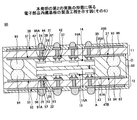
図33を参照するに、第2の実施の形態の第4変形例に係る電子部品内蔵基板130は、第2の実施の形態の電子部品内蔵基板90の構成に、さらにソルダーレジスト層131,132を設けた以外は、電子部品内蔵基板90と同様に構成される。
Referring to FIG. 33, an electronic component built-in
ソルダーレジスト層131は、第1の配線基板11に設けられている。ソルダーレジスト層131は、パッド部42及び第1の導電性ボール93の配設領域を除いた部分の配線パターン37を覆うように、配線基板本体35の面35Aに設けられている。
The solder resist
ソルダーレジスト層132は、第2の配線基板12に設けられている。ソルダーレジスト層132は、パッド部56及び第2の導電性ボール94の配設領域を除いた部分の配線パターン51を覆うように、配線基板本体47の面47Aに設けられている。
The solder resist
本実施の形態の第4変形例に係る電子部品内蔵基板によれば、配線基板本体35の面35Aに、パッド部42及び第1の導電性ボール93の配設領域を除いた部分の配線パターン37を覆うソルダーレジスト層131を設けることにより、第1の配線基板11に第1の導電性ボール93を接合させる際、溶融したはんだ(第1の導電性ボール93を構成するはんだ)の流出により、隣り合う配線パターン37がショートすることを防止できる。
According to the electronic component built-in substrate according to the fourth modification of the present embodiment, the wiring pattern of the portion excluding the arrangement area of the
また、配線基板本体47の面47Aに、パッド部56及び第2の導電性ボール94の配設領域を除いた部分の配線パターン51を覆うソルダーレジスト層132を設けることにより、第2の配線基板12と第2の導電性ボール94とを接合させる際、溶融したはんだ(第2の導電性ボール94を構成するはんだ)の流出により、隣り合う配線パターン51がショートすることを防止できる。
Further, by providing a solder resist
なお、上記構成とされた第2の実施の形態の第4変形例に係る電子部品内蔵基板130は、第2の実施の形態の電子部品内蔵基板90と同様な効果を得ることができる。
The electronic component built-in
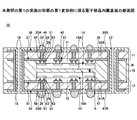
図34〜図37は、本発明の第2の実施の形態の第4変形例に係る電子部品内蔵基板の製造工程を示す図である。図34〜図37において、第2の実施の形態の第4変形例に係る電子部品内蔵基板130と同一構成部分には同一符号を付す。
34 to 37 are views showing manufacturing steps of the electronic component built-in substrate according to the fourth modification example of the second embodiment of the present invention. 34 to 37, the same components as those of the electronic component built-in
図34〜図37を参照して、本発明の第2の実施の形態の第4変形例に係る電子部品内蔵基板130の製造方法について説明する。
With reference to FIGS. 34 to 37, a method of manufacturing the electronic component built-in
始めに、図34に示す工程では、第1の実施の形態で説明した図12に示す第1の配線基板11を形成した後、配線基板本体35の面35Aに、パッド部42及び第1の導電性ボール93の配設領域を除いた部分の配線パターン37を覆うソルダーレジスト層131を形成すると共に、配線基板本体35の面35Bに、パッド部44を除いた部分の配線パターン38を覆うソルダーレジスト層96を形成する。
First, in the process shown in FIG. 34, after the
次いで、図35に示す工程では、パッド部42に第1の電子部品14を表面実装(第1の電子部品実装工程)し、その後、第1の導電性ボール93の配設領域に対応する部分の配線パターン37に第1の導電性ボール93を形成する。第1の電子部品実装工程では、例えば、パッド部42上に溶融させたはんだ31を準備し、溶融させたはんだ31に第1の電子部品14の電極パッド61に設けられたバンプ28を押し当てることで、パッド部42上にバンプ28を固定する。
Next, in the step shown in FIG. 35, the first
このように、配線基板本体35の面35Aに、パッド部42及び第1の導電性ボール93の配設領域を除いた部分の配線パターン37を覆うソルダーレジスト層131を形成し、その後、パッド部42に第1の電子部品14を表面実装し、配線パターン37に第1の導電性ボール93を形成することで、溶融したはんだ(具体的には、はんだ31及び第1の導電性ボール93を構成するはんだ)により、隣り合う配線パターン37がショートすることを防止できる。
As described above, the solder resist
次いで、図36に示す工程では、第1の実施の形態で説明した図14に示す第2の配線基板12を形成した後、配線基板本体47の面47Aに、パッド部56及び第2の導電性ボール94の配設領域を除いた部分の配線パターン51を覆うソルダーレジスト層132を形成すると共に、配線基板本体47の面47Bに、パッド部57を除いた部分の配線パターン52を覆うソルダーレジスト層97を形成する。
Next, in the step shown in FIG. 36, after forming the
次いで、図37に示す工程では、パッド部56に第2の電子部品15を表面実装(第2の電子部品実装工程)し、その後、第2の導電性ボール94の配設領域に対応する部分の配線パターン51に第2の導電性ボール94を形成する。第2の電子部品実装工程では、例えば、パッド部56上に溶融させたはんだ32を準備し、溶融させたはんだ32に第2の電子部品15の電極パッド63に設けられたバンプ29を押し当てることで、パッド部56上にバンプ29を固定する。
Next, in the step shown in FIG. 37, the second
このように、配線基板本体47の面47Aに、パッド部56及び第2の導電性ボール94の配設領域を除いた部分の配線パターン51を覆うソルダーレジスト層132を形成し、その後、パッド部56に第2の電子部品15を表面実装し、配線パターン51に第2の導電性ボール94を形成することで、溶融したはんだ(具体的には、はんだ32及び第2の導電性ボール94を構成するはんだ)により、隣り合う配線パターン51がショートすることを防止できる。
In this manner, the solder resist
その後、本実施の形態で説明した図30〜図32に示す工程と同様な処理を行うことで、本実施の形態の第4変形例に係る電子部品内蔵基板130が製造される。
Thereafter, the electronic component built-in
本実施の形態の第4変形例に係る電子部品内蔵基板の製造方法によれば、配線基板本体35の面35Aに、パッド部42及び第1の導電性ボール93の配設領域を除いた部分の配線パターン37を覆うソルダーレジスト層131を形成し、その後、パッド部42に第1の電子部品14を表面実装し、配線パターン37に第1の導電性ボール93を形成することで、溶融したはんだ(具体的には、はんだ31及び第1の導電性ボール93を構成するはんだ)により、隣り合う配線パターン37がショートすることを防止できる。
According to the method for manufacturing the electronic component built-in substrate according to the fourth modification of the present embodiment, the portion excluding the area where the
また、配線基板本体47の面47Aに、パッド部56及び第2の導電性ボール94の配設領域を除いた部分の配線パターン51を覆うソルダーレジスト層132を形成し、その後、パッド部56に第2の電子部品15を表面実装し、配線パターン51に第2の導電性ボール94を形成することで、溶融したはんだ(具体的には、はんだ32及び第2の導電性ボール94を構成するはんだ)により、隣り合う配線パターン51がショートすることを防止できる。
Further, a solder resist
以上、本発明の好ましい実施の形態について詳述したが、本発明はかかる特定の実施の形態に限定されるものではなく、特許請求の範囲内に記載された本発明の要旨の範囲内において、種々の変形・変更が可能である。 The preferred embodiments of the present invention have been described in detail above, but the present invention is not limited to such specific embodiments, and within the scope of the present invention described in the claims, Various modifications and changes are possible.
例えば、上記説明した電子部品内蔵基板90,100,105,110,130では、第1の電子部品14と第2の電子部品15との間に隙間Aを形成した場合を例に挙げて説明したが、第1の電子部品14の面14Aと第2の電子部品15の面15Aとが接触するように、第1及び第2の電子部品14,15を配置してもよい。
For example, in the electronic component built-in
本発明は、複数の電子部品の内蔵した電子部品内蔵基板及びその製造方法に適用できる。 The present invention can be applied to an electronic component built-in substrate in which a plurality of electronic components are built and a manufacturing method thereof.
10,70,75,80,90,100,105,110,130 電子部品内蔵基板
11 第1の配線基板
12 第2の配線基板
14,81 第1の電子部品
14A,15A,35A,35B,47A,47B,76A,81A 面
15,76 第2の電子部品
16,92 樹脂部材
16A,92A 上面
16B,92B 下面
18 貫通孔
19 貫通電極
22,96,97,131,132 ソルダーレジスト層
22A,22B,96A,97A 開口部
24 第1の外部接続端子
25 第2の外部接続端子
28,29 バンプ
31,32 はんだ
35,47 配線基板本体
37〜39,51〜53 配線パターン
42,44,56,57 パッド部
61,63 電極パッド
71 第1のアンダーフィル樹脂
72 第2のアンダーフィル樹脂
85 第1の貫通部
87,125 積層体
93 第1の導電性ボール
94 第2の導電性ボール
122 第2の貫通部
A 隙間
B,C,D,E 厚さ
10, 70, 75, 80, 90, 100, 105, 110, 130 Electronic component built-in
Claims (13)
前記第1の配線パターンに表面実装された第1の電子部品と、
第2の配線基板本体及び該第2の配線基板本体の第1の面に設けられた第2の配線パターンを有し、前記第1の配線基板本体の第1の面と前記第2の配線基板本体の第1の面とが対向するように、前記第1の配線基板の下方に配置された第2の配線基板と、
前記第2の配線パターンに表面実装されると共に、前記第1の電子部品と対向するように配置された第2の電子部品と、
前記第1の電子部品が接続された前記第1の配線基板と、前記第2の電子部品が接続された前記第2の配線基板との間を封止する樹脂部材と、を有することを特徴とする電子部品内蔵基板。 A first wiring board having a first wiring board body and a first wiring pattern provided on a first surface of the first wiring board body;
A first electronic component surface-mounted on the first wiring pattern;
A second wiring board body and a second wiring pattern provided on a first surface of the second wiring board body, the first surface of the first wiring board body and the second wiring; A second wiring board disposed below the first wiring board so as to face the first surface of the board body;
A second electronic component that is surface-mounted on the second wiring pattern and arranged to face the first electronic component;
And a resin member for sealing between the first wiring board to which the first electronic component is connected and the second wiring board to which the second electronic component is connected. Electronic component built-in board.
前記第2の配線基板は、前記第2の配線基板本体の第1の面とは反対側に位置する前記第2の配線基板本体の第2の面に、第2の外部接続端子が接続される第4の配線パターンを有し、
前記樹脂部材の母材は、前記第1の配線パターンと前記第2の配線パターンとが対向する部分に前記第1の配線パターンの一部と前記第2の配線パターンの一部とを露出する第2の貫通部を有しており、
前記第2の貫通部の形成領域に対応する部分の前記第1の配線パターンに、前記第2の貫通部に収容される第1の導電性ボールを設け、前記第2の貫通部の形成領域に対応する部分の前記第2の配線パターンに、前記第2の貫通部に収容される第2の導電性ボールを設けると共に、前記第1の導電性ボールと前記第2の導電性ボールとを接触させたことを特徴とする請求項1ないし6のうち、いずれか1項記載の電子部品内蔵基板。 In the first wiring board, a first external connection terminal is connected to a second surface of the first wiring board body located on the opposite side of the first surface of the first wiring board body. A third wiring pattern
The second wiring board has a second external connection terminal connected to a second surface of the second wiring board body located on the opposite side of the first surface of the second wiring board body. A fourth wiring pattern
The base material of the resin member exposes a part of the first wiring pattern and a part of the second wiring pattern at a portion where the first wiring pattern and the second wiring pattern face each other. Having a second penetration,
A first conductive ball accommodated in the second through portion is provided in a portion of the first wiring pattern corresponding to the second through portion forming region, and the second through portion forming region is provided. A second conductive ball accommodated in the second penetrating portion is provided in the second wiring pattern at a portion corresponding to the first wiring ball, and the first conductive ball and the second conductive ball are provided. The electronic component built-in substrate according to claim 1, wherein the electronic component-embedded substrate is in contact with each other.
前記第2の配線基板本体に、前記第2の配線パターンと前記第4の配線パターンとを電気的に接続する配線パターンを設けたことを特徴とする請求項7記載の電子部品内蔵基板。 In the first wiring board body, a wiring pattern for electrically connecting the first wiring pattern and the third wiring pattern is provided, and
8. The electronic component built-in board according to claim 7, wherein a wiring pattern for electrically connecting the second wiring pattern and the fourth wiring pattern is provided on the second wiring board main body.
前記第2の配線基板は、前記第2の配線基板本体の第1の面とは反対側に位置する前記第2の配線基板本体の第2の面に、第2の外部接続端子が接続される第4の配線パターンを有しており、
前記第1の配線基板本体、前記樹脂部材、及び前記第2の配線基板本体を貫通すると共に、前記第1乃至第4の配線パターンと接続された貫通電極を設けたことを特徴とする請求項1ないし6のうち、いずれか1項記載の電子部品内蔵基板。 In the first wiring board, a first external connection terminal is connected to a second surface of the first wiring board body located on the opposite side of the first surface of the first wiring board body. A third wiring pattern
The second wiring board has a second external connection terminal connected to a second surface of the second wiring board body located on the opposite side of the first surface of the second wiring board body. A fourth wiring pattern,
The penetrating electrode that penetrates through the first wiring board main body, the resin member, and the second wiring board main body and is connected to the first to fourth wiring patterns is provided. The electronic component built-in substrate according to any one of 1 to 6.
前記第1の配線パターンに第1の電子部品を表面実装する第1の電子部品実装工程と、
第2の配線基板本体及び該第2の配線基板本体の第1の面に設けられた第2の配線パターンを備えた第2の配線基板を形成する第2の配線基板形成工程と、
前記第2の配線パターンに第2の電子部品を表面実装する第2の電子部品実装工程と、
板状とされ、前記第1及び第2の電子部品が収容される第1の貫通部を有すると共に、半硬化状態とされた樹脂部材を形成する樹脂部材形成工程と、
前記第1の貫通部に、前記第1の配線基板に表面実装された前記第1の電子部品と前記第2の配線基板に表面実装された前記第2の電子部品とを挿入して、前記第1の電子部品及び前記第2の電子部品を対向配置させることにより、前記第1の電子部品が表面実装された第1の配線基板と、前記半硬化状態とされた樹脂部材と、前記第2の電子部品が表面実装された第2の配線基板とが積層された積層体を形成する積層体形成工程と、
前記積層体を加熱した状態でプレスして、前記半硬化状態とされた樹脂部材を完全に硬化させることにより、前記第1の電子部品が表面実装された前記第1の配線基板と、前記第2の電子部品が表面実装された前記第2の配線基板との間を封止する封止工程と、を含むことを特徴とする電子部品内蔵基板の製造方法。 A first wiring board forming step of forming a first wiring board having a first wiring board main body and a first wiring pattern provided on a first surface of the first wiring board main body;
A first electronic component mounting step of surface-mounting the first electronic component on the first wiring pattern;
A second wiring board forming step of forming a second wiring board having a second wiring board body and a second wiring pattern provided on the first surface of the second wiring board body;
A second electronic component mounting step of surface mounting the second electronic component on the second wiring pattern;
A resin member forming step that forms a resin member that is plate-shaped and has a first through portion in which the first and second electronic components are accommodated, and a semi-cured state;
Inserting the first electronic component surface-mounted on the first wiring board and the second electronic component surface-mounted on the second wiring board into the first penetrating portion, and By arranging the first electronic component and the second electronic component to face each other, the first wiring board on which the first electronic component is surface-mounted, the semi-cured resin member, A laminate forming step of forming a laminate in which the second wiring board on which the electronic components of 2 are surface-mounted is laminated;
By pressing the laminate in a heated state and completely curing the resin member in the semi-cured state, the first wiring board on which the first electronic component is surface-mounted, and the first And a sealing step for sealing between the second wiring substrate on which the two electronic components are surface-mounted.
前記第2の配線基板形成工程では、前記第2の電子部品の実装領域以外に配置された部分の前記第2の配線パターンに、前記第1の導電性ボールと対向する第2の導電性ボールを形成すると共に、前記第2の配線基板本体の第1の面とは反対側に位置する前記第2の配線基板本体の第2の面に、第2の外部接続端子が接続され、前記第2の配線パターンと電気的に接続される第4の配線パターンを形成し、
前記樹脂部材形成工程では、前記第1の電子部品の実装領域以外に配置された部分の前記第1の配線パターンと、前記第2の電子部品の実装領域以外に配置された部分の前記第2の配線パターンとの間に位置する部分の前記半硬化状態とされた樹脂部材に、前記第1及び第2の導電性ボールを収容する第2の貫通部を形成し、
前記封止工程では、前記プレスにより前記第1の導電性ボールと前記第2の導電性ボールとを接触させると共に、完全に硬化した前記樹脂部材により前記第1の電子部品が表面実装された第1の配線基板と、前記第2の電子部品が表面実装された第2の配線基板との間を封止することを特徴とする請求項10記載の電子部品内蔵基板の製造方法。 In the first wiring board forming step, a first conductive ball is formed on the first wiring pattern in a portion arranged outside the mounting area of the first electronic component, and the first wiring board is formed. A first external connection terminal is connected to the second surface of the first wiring board main body located on the opposite side of the first surface of the main body, and is electrically connected to the first wiring pattern. Forming a third wiring pattern;
In the second wiring board forming step, a second conductive ball facing the first conductive ball is formed on a portion of the second wiring pattern arranged outside the mounting area of the second electronic component. And a second external connection terminal is connected to the second surface of the second wiring board body located on the opposite side of the first surface of the second wiring board body. Forming a fourth wiring pattern electrically connected to the second wiring pattern;
In the resin member forming step, the first wiring pattern in a portion arranged outside the mounting region of the first electronic component and the second of the portion arranged outside the mounting region of the second electronic component. Forming a second penetrating portion that accommodates the first and second conductive balls in the semi-cured resin member in a portion located between the wiring pattern and the wiring pattern;
In the sealing step, the first conductive ball and the second conductive ball are brought into contact with each other by the pressing, and the first electronic component is surface-mounted by the completely cured resin member. 11. The method of manufacturing a substrate with built-in electronic components according to claim 10, wherein the space between one wiring substrate and the second wiring substrate on which the second electronic component is surface-mounted is sealed.
前記封止工程において、前記第1の電子部品と前記第2の電子部品との間は、前記プリプレグ樹脂に含まれる樹脂により封止されることを特徴とする請求項10または11記載の電子部品内蔵基板の製造方法。 The resin member is a prepreg resin,
The electronic component according to claim 10 or 11, wherein, in the sealing step, a gap between the first electronic component and the second electronic component is sealed with a resin contained in the prepreg resin. A method for manufacturing a built-in substrate.
Priority Applications (2)
| Application Number | Priority Date | Filing Date | Title |
|---|---|---|---|
| JP2008315513A JP2010141098A (en) | 2008-12-11 | 2008-12-11 | Substrate with built-in electronic components and method of manufacturing the same |
| US12/635,066 US8559184B2 (en) | 2008-12-11 | 2009-12-10 | Electronic component built-in substrate and method of manufacturing the same |
Applications Claiming Priority (1)
| Application Number | Priority Date | Filing Date | Title |
|---|---|---|---|
| JP2008315513A JP2010141098A (en) | 2008-12-11 | 2008-12-11 | Substrate with built-in electronic components and method of manufacturing the same |
Publications (2)
| Publication Number | Publication Date |
|---|---|
| JP2010141098A true JP2010141098A (en) | 2010-06-24 |
| JP2010141098A5 JP2010141098A5 (en) | 2012-01-12 |
Family
ID=42240265
Family Applications (1)
| Application Number | Title | Priority Date | Filing Date |
|---|---|---|---|
| JP2008315513A Pending JP2010141098A (en) | 2008-12-11 | 2008-12-11 | Substrate with built-in electronic components and method of manufacturing the same |
Country Status (2)
| Country | Link |
|---|---|
| US (1) | US8559184B2 (en) |
| JP (1) | JP2010141098A (en) |
Families Citing this family (20)
| Publication number | Priority date | Publication date | Assignee | Title |
|---|---|---|---|---|
| JP2011187681A (en) * | 2010-03-09 | 2011-09-22 | Toshiba Corp | Method for manufacturing semiconductor device and semiconductor device |
| WO2012005236A1 (en) * | 2010-07-06 | 2012-01-12 | 株式会社フジクラ | Laminated wiring board and manufacturing method for same |
| US8472207B2 (en) * | 2011-01-14 | 2013-06-25 | Harris Corporation | Electronic device having liquid crystal polymer solder mask and outer sealing layers, and associated methods |
| US8649183B2 (en) | 2011-02-10 | 2014-02-11 | Mulpin Research Laboratories, Ltd. | Electronic assembly |
| TWI425886B (en) * | 2011-06-07 | 2014-02-01 | 欣興電子股份有限公司 | Encapsulation structure embedded with electronic components and method of manufacturing the same |
| KR20130097481A (en) * | 2012-02-24 | 2013-09-03 | 삼성전자주식회사 | Printed circuit board(pcb), and memory module comprising the same pcb |
| JP5285819B1 (en) * | 2012-11-07 | 2013-09-11 | 太陽誘電株式会社 | Electronic circuit module |
| KR101420526B1 (en) * | 2012-11-29 | 2014-07-17 | 삼성전기주식회사 | Substrate embedding electronic component and manufacturing mehtod thereof |
| US10264664B1 (en) * | 2015-06-04 | 2019-04-16 | Vlt, Inc. | Method of electrically interconnecting circuit assemblies |
| US10785871B1 (en) * | 2018-12-12 | 2020-09-22 | Vlt, Inc. | Panel molded electronic assemblies with integral terminals |
| DE102017209249A1 (en) * | 2017-05-31 | 2018-12-06 | Fraunhofer-Gesellschaft zur Förderung der angewandten Forschung e.V. | METHOD FOR PRODUCING A PACKAGE AND PACKAGE |
| KR20190012485A (en) * | 2017-07-27 | 2019-02-11 | 삼성전기주식회사 | Printed circuit board and method of fabricating the same |
| WO2019026835A1 (en) * | 2017-08-04 | 2019-02-07 | 株式会社フジクラ | Multilayer printed wiring board manufacturing method and multilayer printed wiring board |
| US10553563B2 (en) * | 2018-05-30 | 2020-02-04 | Epistar Corporation | Electronic device |
| US10790232B2 (en) * | 2018-09-15 | 2020-09-29 | International Business Machines Corporation | Controlling warp in semiconductor laminated substrates with conductive material layout and orientation |
| KR102854182B1 (en) * | 2020-07-06 | 2025-09-03 | 삼성전기주식회사 | Printed circuit board with embedded electronic component |
| KR20220106561A (en) * | 2021-01-22 | 2022-07-29 | 삼성전자주식회사 | Dual side surface mounted device type electronic component assembly and electronic device including thereof |
| CN115954330A (en) * | 2023-02-03 | 2023-04-11 | 长鑫存储技术有限公司 | Encapsulation structure and preparation method thereof |
| DE112023005761T5 (en) * | 2023-02-09 | 2025-12-11 | Microchip Technology Caldicot Limited | PCB stack with embedded component assembly and sintered vias |
| US20250105162A1 (en) * | 2023-09-21 | 2025-03-27 | JCET STATS ChipPAC Korea Limited | Semiconductor Device and Method of Forming Fine-Pitch Interconnection Using Insulating Layer |
Citations (5)
| Publication number | Priority date | Publication date | Assignee | Title |
|---|---|---|---|---|
| JP2005142178A (en) * | 2003-11-04 | 2005-06-02 | Cmk Corp | Multi-layer printed wiring board with built-in electronic components |
| JP2006156669A (en) * | 2004-11-29 | 2006-06-15 | Dainippon Printing Co Ltd | Component built-in wiring board, method of manufacturing component built-in wiring board |
| JP2007173570A (en) * | 2005-12-22 | 2007-07-05 | Matsushita Electric Ind Co Ltd | Semiconductor device, method for manufacturing the same, and electronic apparatus including the semiconductor device |
| JP2008205290A (en) * | 2007-02-21 | 2008-09-04 | Fujitsu Ltd | Component built-in substrate and manufacturing method thereof |
| JP2008294475A (en) * | 2001-10-18 | 2008-12-04 | Panasonic Corp | Manufacturing method of module with built-in components |
Family Cites Families (5)
| Publication number | Priority date | Publication date | Assignee | Title |
|---|---|---|---|---|
| JP3619395B2 (en) * | 1999-07-30 | 2005-02-09 | 京セラ株式会社 | Semiconductor device built-in wiring board and manufacturing method thereof |
| KR100335717B1 (en) * | 2000-02-18 | 2002-05-08 | 윤종용 | High Density Memory Card |
| US7485489B2 (en) * | 2002-06-19 | 2009-02-03 | Bjoersell Sten | Electronics circuit manufacture |
| US7394663B2 (en) * | 2003-02-18 | 2008-07-01 | Matsushita Electric Industrial Co., Ltd. | Electronic component built-in module and method of manufacturing the same |
| US8093506B2 (en) * | 2006-12-21 | 2012-01-10 | Ngk Spark Plug Co., Ltd. | Multilayer wiring board and power supply structure to be embedded in multilayer wiring board |
-
2008
- 2008-12-11 JP JP2008315513A patent/JP2010141098A/en active Pending
-
2009
- 2009-12-10 US US12/635,066 patent/US8559184B2/en not_active Expired - Fee Related
Patent Citations (5)
| Publication number | Priority date | Publication date | Assignee | Title |
|---|---|---|---|---|
| JP2008294475A (en) * | 2001-10-18 | 2008-12-04 | Panasonic Corp | Manufacturing method of module with built-in components |
| JP2005142178A (en) * | 2003-11-04 | 2005-06-02 | Cmk Corp | Multi-layer printed wiring board with built-in electronic components |
| JP2006156669A (en) * | 2004-11-29 | 2006-06-15 | Dainippon Printing Co Ltd | Component built-in wiring board, method of manufacturing component built-in wiring board |
| JP2007173570A (en) * | 2005-12-22 | 2007-07-05 | Matsushita Electric Ind Co Ltd | Semiconductor device, method for manufacturing the same, and electronic apparatus including the semiconductor device |
| JP2008205290A (en) * | 2007-02-21 | 2008-09-04 | Fujitsu Ltd | Component built-in substrate and manufacturing method thereof |
Also Published As
| Publication number | Publication date |
|---|---|
| US8559184B2 (en) | 2013-10-15 |
| US20100149768A1 (en) | 2010-06-17 |
Similar Documents
| Publication | Publication Date | Title |
|---|---|---|
| JP2010141098A (en) | Substrate with built-in electronic components and method of manufacturing the same | |
| CN101115352B (en) | Multilayered printed wiring board and method for manufacturing the same | |
| JP5427305B1 (en) | Component-embedded substrate, manufacturing method thereof, and mounting body | |
| KR101438915B1 (en) | The printed circuit board and the method for manufacturing the same | |
| CN104869753A (en) | Printed Circuit Board And Method Of Manufacturing The Same | |
| JP2011249759A (en) | Printed circuit board having electronic component and method for manufacturing the same | |
| JP2017034059A (en) | Printed wiring board, semiconductor package and printed wiring board manufacturing method | |
| JP5454681B2 (en) | Module substrate and manufacturing method thereof | |
| JP5191889B2 (en) | Manufacturing method of component built-in wiring board | |
| JP2007266196A (en) | Multilayer printed wiring board and manufacturing method thereof | |
| JP2017143096A (en) | Wiring board, semiconductor device and wiring board manufacturing method | |
| JP5462450B2 (en) | Component built-in printed wiring board and method for manufacturing component built-in printed wiring board | |
| JP2006156669A (en) | Component built-in wiring board, method of manufacturing component built-in wiring board | |
| JP2009135391A (en) | Electronic device and manufacturing method thereof | |
| JP2007295008A (en) | Manufacturing method of wiring board with built-in electronic components | |
| JP2008311508A (en) | Electronic component package and manufacturing method thereof | |
| JP5671857B2 (en) | Manufacturing method of wiring board with embedded parts | |
| JP2008181921A (en) | Electronic component-embedded substrate, electronic device using the same, and manufacturing method thereof | |
| JP6068167B2 (en) | Wiring board and manufacturing method thereof | |
| JP4978709B2 (en) | Electronic component built-in wiring board | |
| JP5882100B2 (en) | Component built-in circuit board | |
| JP5761405B2 (en) | Electronic component built-in wiring board | |
| JP2012109615A (en) | Wiring board with built-in electronic component | |
| JP2007335487A (en) | Semiconductor device and manufacturing method thereof | |
| JP2011077195A (en) | Component mounting substrate and method of manufacturing component mounting substrate |
Legal Events
| Date | Code | Title | Description |
|---|---|---|---|
| A521 | Request for written amendment filed |
Free format text: JAPANESE INTERMEDIATE CODE: A523 Effective date: 20111116 |
|
| A621 | Written request for application examination |
Free format text: JAPANESE INTERMEDIATE CODE: A621 Effective date: 20111116 |
|
| A977 | Report on retrieval |
Free format text: JAPANESE INTERMEDIATE CODE: A971007 Effective date: 20130130 |
|
| A131 | Notification of reasons for refusal |
Free format text: JAPANESE INTERMEDIATE CODE: A131 Effective date: 20130205 |
|
| A02 | Decision of refusal |
Free format text: JAPANESE INTERMEDIATE CODE: A02 Effective date: 20130604 |