JP2010093074A - Flexible printed wiring board sheet and method for manufacturing the same - Google Patents
Flexible printed wiring board sheet and method for manufacturing the same Download PDFInfo
- Publication number
- JP2010093074A JP2010093074A JP2008262028A JP2008262028A JP2010093074A JP 2010093074 A JP2010093074 A JP 2010093074A JP 2008262028 A JP2008262028 A JP 2008262028A JP 2008262028 A JP2008262028 A JP 2008262028A JP 2010093074 A JP2010093074 A JP 2010093074A
- Authority
- JP
- Japan
- Prior art keywords
- outer frame
- flexible printed
- printed wiring
- wiring board
- layer
- Prior art date
- Legal status (The legal status is an assumption and is not a legal conclusion. Google has not performed a legal analysis and makes no representation as to the accuracy of the status listed.)
- Granted
Links
- 238000000034 method Methods 0.000 title claims abstract description 52
- 238000004519 manufacturing process Methods 0.000 title claims abstract description 31
- 238000007747 plating Methods 0.000 claims abstract description 160
- 239000000047 product Substances 0.000 claims abstract description 68
- 239000004020 conductor Substances 0.000 claims abstract description 61
- 239000000463 material Substances 0.000 claims abstract description 17
- 229910052751 metal Inorganic materials 0.000 claims abstract description 16
- 239000002184 metal Substances 0.000 claims abstract description 16
- 239000013067 intermediate product Substances 0.000 claims abstract description 7
- 229910052802 copper Inorganic materials 0.000 claims description 57
- 239000010949 copper Substances 0.000 claims description 57
- RYGMFSIKBFXOCR-UHFFFAOYSA-N Copper Chemical compound [Cu] RYGMFSIKBFXOCR-UHFFFAOYSA-N 0.000 claims description 56
- 230000008569 process Effects 0.000 claims description 44
- 230000003247 decreasing effect Effects 0.000 claims description 6
- 239000012212 insulator Substances 0.000 claims description 5
- 230000009467 reduction Effects 0.000 claims description 3
- 230000007423 decrease Effects 0.000 claims 2
- 239000000758 substrate Substances 0.000 claims 1
- 239000010409 thin film Substances 0.000 description 21
- 239000010408 film Substances 0.000 description 19
- PCHJSUWPFVWCPO-UHFFFAOYSA-N gold Chemical compound [Au] PCHJSUWPFVWCPO-UHFFFAOYSA-N 0.000 description 18
- 239000010931 gold Substances 0.000 description 18
- 229910052737 gold Inorganic materials 0.000 description 18
- 239000011888 foil Substances 0.000 description 11
- 239000004642 Polyimide Substances 0.000 description 10
- 229920001721 polyimide Polymers 0.000 description 10
- 229910001220 stainless steel Inorganic materials 0.000 description 9
- 239000010935 stainless steel Substances 0.000 description 9
- 230000000694 effects Effects 0.000 description 8
- 238000004080 punching Methods 0.000 description 8
- 230000009471 action Effects 0.000 description 6
- PXHVJJICTQNCMI-UHFFFAOYSA-N Nickel Chemical compound [Ni] PXHVJJICTQNCMI-UHFFFAOYSA-N 0.000 description 4
- 238000010586 diagram Methods 0.000 description 4
- 230000004048 modification Effects 0.000 description 4
- 238000012986 modification Methods 0.000 description 4
- 238000009826 distribution Methods 0.000 description 3
- 238000007772 electroless plating Methods 0.000 description 3
- VYZAMTAEIAYCRO-UHFFFAOYSA-N Chromium Chemical compound [Cr] VYZAMTAEIAYCRO-UHFFFAOYSA-N 0.000 description 2
- 229910052804 chromium Inorganic materials 0.000 description 2
- 239000011651 chromium Substances 0.000 description 2
- 238000009713 electroplating Methods 0.000 description 2
- 239000007788 liquid Substances 0.000 description 2
- 229910052759 nickel Inorganic materials 0.000 description 2
- 230000008054 signal transmission Effects 0.000 description 2
- 238000004544 sputter deposition Methods 0.000 description 2
- 238000012935 Averaging Methods 0.000 description 1
- JPVYNHNXODAKFH-UHFFFAOYSA-N Cu2+ Chemical compound [Cu+2] JPVYNHNXODAKFH-UHFFFAOYSA-N 0.000 description 1
- 230000008901 benefit Effects 0.000 description 1
- 230000015572 biosynthetic process Effects 0.000 description 1
- 230000008859 change Effects 0.000 description 1
- 150000001879 copper Chemical class 0.000 description 1
- 229910001431 copper ion Inorganic materials 0.000 description 1
- 238000007865 diluting Methods 0.000 description 1
- 238000000059 patterning Methods 0.000 description 1
- 230000035699 permeability Effects 0.000 description 1
- 239000002244 precipitate Substances 0.000 description 1
- 230000007261 regionalization Effects 0.000 description 1
Images


Abstract
Description
本発明は、フレキシブルプリント配線板が複数設けられたフレキシブルプリント配線板シート、およびその製造方法に関するものである。 The present invention relates to a flexible printed wiring board sheet provided with a plurality of flexible printed wiring boards, and a method for manufacturing the same.
ハードディスク装置の磁気ヘッドを支持する支持金属箔と、信号伝達のための配線とが一体化された配線板(以下、「磁気ヘッド配線板」と記す)は、垂直磁気記録方式などの情報密度の増大にともなってさらに需要が増大している。磁気ヘッド配線板は、シート単位で製造され、1枚のシート内に、数十個、設けられている。これを、フレキシブルプリント配線板シートと呼ぶこととする。1枚のフレキシブルプリント配線板シート内には、めっきフレームが巡らされ、そのめっきフレームに繋がれて数十個の同一配線パターン(磁気ヘッド配線板)が形成されている。配線、めっきフレーム、めっきリード部等は、銅めっき層によって形成されている。また、上記のめっきフレームを用いて、配線の所定部分(接続部)に金めっき層を形成する。個々の磁気ヘッド配線板では、複数の配線が並行しており、配線の根元からめっきリード部が延びて、めっきフレームと連結して導通をとる。一方、反対側の先端では、上記複数の配線が延び出している。上記の金めっき層の形成、その他の一連の処理の後、フレキシブルプリント配線板シートを完成し、そのフレキシブルプリント配線板シートの状態で、中間製品メーカまたは磁気ヘッド配線板組み込みメーカに出荷される。 A wiring board (hereinafter referred to as “magnetic head wiring board”) in which a supporting metal foil for supporting a magnetic head of a hard disk device and wiring for signal transmission are integrated is an information density of a perpendicular magnetic recording system or the like. With the increase, demand is further increasing. The magnetic head wiring board is manufactured in units of sheets, and several tens of magnetic head wiring boards are provided in one sheet. This is called a flexible printed wiring board sheet. A single flexible printed wiring board sheet is provided with a plating frame, and several tens of identical wiring patterns (magnetic head wiring boards) are formed connected to the plating frame. Wiring, a plating frame, a plating lead part, etc. are formed of a copper plating layer. Further, a gold plating layer is formed on a predetermined portion (connection portion) of the wiring using the above-described plating frame. In each magnetic head wiring board, a plurality of wirings are arranged in parallel, and the plating lead portion extends from the root of the wiring and is connected to the plating frame to be conductive. On the other hand, at the tip on the opposite side, the plurality of wires extend. After the formation of the gold plating layer and other series of processes, a flexible printed wiring board sheet is completed, and the flexible printed wiring board sheet is shipped to an intermediate product manufacturer or a magnetic head wiring board embedded manufacturer.
上記より、フレキシブルプリント配線板シートの製造において、配線の銅めっき、その配線の所定部への金めっきなど、めっき処理が重要な処理であることが分かる。とくに高い精度の厚みをもち、全体にわたって均一な厚みのめっき層を得ることは重要である。このため、フレキシブルプリント配線板シートのめっき処理の際に、めっき液をめっき槽の壁面等に噴射して反射流を生じさせ、この反射流の中に、陰極側の回路基板および陽極を面が並行するように配置してめっき処理する方法が開示されている(特許文献1)。
上記の反射流を生じさせて反射流中に回路基板等を並行配置する方策は、一定の効果はある。しかし、フレキシブルプリント配線板シートの外枠部が広く、フレキシブルプリント配線板が配列されるシート内側の製品領域の面積よりも、外枠部の面積が非常に大きい場合、製品領域に対する電流の調整が困難になる。とくに外枠部の端部は、対面相手のめっき金属板との位置関係の少しのずれによって、めっき液内を巡ってきて析出する金属が多くあり、端部特有の不安定作用を生じる。この結果、種類の異なるフレキシブルプリント配線板を、フレキシブルプリント配線板シートの形態で製造するとき、種類に応じて製品領域に対するめっき処理条件(電流密度など)をきめ細かく調整できなくなる。たとえば、めっき膜厚を、装置全体のトータル電流と時間とで、意図した厚みに精度よく形成することが困難になる。なお、各めっき処理時に、外枠部では、導体薄膜が露出している。金めっき処理は、所定領域に限定されるが、導体薄膜に加えて銅めっき配線層が露出している。
外枠部をなくすことができれば、製品領域の電流密度のきめ細かい調整は、しやすくなる。しかし、ガイドマークの配置、めっきマスクの露光時の位置合わせ保持部、ハンドリング、製品領域を保護する強度確保などのために、外枠部は必要である。このため、外枠部を備えた上で、フレキシブルプリント配線板の種類に応じて、製品領域に対する電流調整などが可能な対策が要求されている。
本発明は、外枠部をもつフレキシブルプリント配線板シートの製造工程のめっき処理において、製品領域の電流調整がしやすい、フレキシブルプリント配線板シートおよびその製造方法を提供することを目的とする。
The above-described measures for generating a reflected flow and arranging circuit boards and the like in the reflected flow have certain effects. However, if the outer frame part of the flexible printed wiring board sheet is wide and the area of the outer frame part is much larger than the area of the product area inside the sheet on which the flexible printed wiring board is arranged, the current adjustment for the product area is not possible. It becomes difficult. In particular, the end portion of the outer frame portion has a large amount of metal that precipitates around the plating solution due to a slight shift in the positional relationship with the plated metal plate of the facing counterpart, and causes an unstable action peculiar to the end portion. As a result, when different types of flexible printed wiring boards are manufactured in the form of a flexible printed wiring board sheet, it becomes impossible to finely adjust the plating treatment conditions (current density, etc.) for the product region according to the types. For example, it becomes difficult to accurately form the plating film thickness to the intended thickness with the total current and time of the entire apparatus. In each plating process, the conductor thin film is exposed at the outer frame portion. Although the gold plating process is limited to a predetermined region, the copper plating wiring layer is exposed in addition to the conductor thin film.
If the outer frame portion can be eliminated, fine adjustment of the current density in the product area is facilitated. However, the outer frame portion is necessary for the arrangement of the guide marks, the alignment holding portion at the time of exposure of the plating mask, the handling, the securing of the strength for protecting the product area, and the like. For this reason, after providing an outer frame part, the countermeasure which can adjust the electric current etc. with respect to a product area | region is requested | required according to the kind of flexible printed wiring board.
An object of this invention is to provide the flexible printed wiring board sheet | seat which is easy to adjust the electric current of a product area | region, and its manufacturing method in the plating process of the manufacturing process of the flexible printed wiring board sheet | seat which has an outer frame part.
本発明のフレキシブルプリント配線板シートの製造方法は、めっき金属層を含むフレキシブルプリント配線板を複数備えるフレキシブルプリント配線板シートを製造する。フレキシブルプリント配線板シートは、導体層を含む外枠部と、該外枠部に取り囲まれてフレキシブルプリント配線板が形成される製品領域とを有し、この製造方法では、フレキシブルプリント配線板シートの中間製品である基材シートに金属層を形成するめっき処理のとき、基材シートの外枠部の導体層へ流れる電流を減少させるために、外枠部電流減少手段を用いることを特徴とする。 The manufacturing method of the flexible printed wiring board sheet | seat of this invention manufactures a flexible printed wiring board sheet | seat provided with two or more flexible printed wiring boards containing a metal plating layer. The flexible printed wiring board sheet has an outer frame portion including a conductor layer, and a product region in which the flexible printed wiring board is formed surrounded by the outer frame portion. In this manufacturing method, the flexible printed wiring board sheet The outer frame portion current reducing means is used to reduce the current flowing to the conductor layer of the outer frame portion of the base material sheet during the plating process for forming the metal layer on the base material sheet as an intermediate product. .
上記の方法によって、めっき処理時に電流を、製品領域に集めることができ、製品領域に対するきめ細かい高精度の電流制御が容易になる。さらに外枠部の端部特有の不安定作用を減少させることができる。製品の要求仕様に応じて、きめ細かくめっき膜厚等を調整でき、高品質を確保することが可能となる。そして製品種類ごとに、めっき厚みの精度を高め、さらに製品領域について均一なめっき膜厚を得ることができる。 By the above method, current can be collected in the product area during the plating process, and fine and precise current control for the product area is facilitated. Furthermore, the unstable action peculiar to the end of the outer frame part can be reduced. The plating film thickness can be finely adjusted according to the required specifications of the product, and high quality can be ensured. And the precision of plating thickness can be improved for every product kind, and also a uniform plating film thickness can be obtained about a product area | region.
上記のめっき処理の前に、外枠部電流減少手段として、導体層の欠落部が外枠部に散在するように、加工し、欠落部が散在する外枠部を持つ基材シートに対してめっき処理をすることができる。これによって、外枠部の強度および把持部分を確保しながら、電流の流れ込み量を減少させ、製品領域へ流れる電流比率を増やして、製品領域に対する高精度の電流調整を容易にすることができる。とくに滑らかな(孔なし)連続平板の端部特有の不安定作用については、欠落部を散在させることで、不安定作用が、辺縁や角部に集中せずに外枠部全体に平均化され、希薄化される。このような不安定作用の平均化・希薄化によって、対面する相手金属板との少しのずれがあっても、大きな影響は発生せず、製品領域の電流制御の精度を高めることができる。この結果、製品領域のめっき厚の精度を高め、かつ製品領域にわたって厚みを均一にすることができる。 Before the above plating treatment, as a means for reducing the outer frame portion current, it is processed so that the missing portions of the conductor layer are scattered in the outer frame portion, and the base sheet having the outer frame portion in which the missing portions are scattered. Plating treatment can be performed. Thereby, while ensuring the strength and gripping portion of the outer frame portion, it is possible to reduce the amount of current flowing in and increase the ratio of the current flowing to the product region, thereby facilitating highly accurate current adjustment for the product region. In particular, the unstable action unique to the edge of a smooth (no hole) continuous plate is scattered over the missing part, so that the unstable action is averaged over the entire outer frame without concentrating on the edges or corners. And diluted. By averaging and diluting such unstable action, even if there is a slight deviation from the opposing metal plate facing, no significant effect occurs, and the accuracy of current control in the product area can be improved. As a result, the accuracy of the plating thickness in the product region can be improved and the thickness can be made uniform over the product region.
上記の導体層欠落部を、ドット状またはメッシュ状の孔とすることができる。これによって、打ち抜き加工などの簡単な加工によって、外枠部の強度と把持部面積を確保しながら、製品領域に対する電流調整の精度を高めることができる。この結果、製品領域のめっき厚の精度を向上し、製品領域にわたってめっき厚を均一にすることができる。 The conductor layer missing portion can be a dot-like or mesh-like hole. Thereby, the accuracy of the current adjustment with respect to the product region can be enhanced by securing the strength of the outer frame portion and the gripping portion area by a simple processing such as punching. As a result, the accuracy of the plating thickness in the product area can be improved, and the plating thickness can be made uniform over the product area.
導体層の欠落部を設けない場合には、外枠部電流減少手段として、めっき処理の前に、製品領域および外枠部の導体層上にレジストパターンを設けことができる。外枠部に囲まれる製品領域は、配線回路を形成するために、めっき処理の前にレジスパターンを必ず形成する。製品領域のレジストパターンと外枠部のレジストパターンとを同時に形成することで、打ち抜き加工等により外枠部に貫通孔をあける工程を追加する必要はなくなる。すなわち、外枠部のレジストパターンのレジスト膜部にはめっき電流は流れず、導体層の欠落部と同じ作用を奏する。これにより、製造期間の短縮、工数の節約、打ち抜き装置などの不要化を得ることができ、全体的にみて、打ち抜き加工等よりも製造コストを削減することができる。また、外枠部の強度確保からも、レジストパターンによるめっき電流制御のほうが好ましい。 When the missing portion of the conductor layer is not provided, a resist pattern can be provided on the product region and the conductor layer of the outer frame portion as the outer frame portion current reducing means before the plating process. In the product region surrounded by the outer frame portion, a resist pattern is always formed before plating in order to form a wiring circuit. By simultaneously forming the resist pattern in the product region and the resist pattern in the outer frame portion, there is no need to add a step of making a through hole in the outer frame portion by punching or the like. That is, the plating current does not flow in the resist film portion of the resist pattern in the outer frame portion, and has the same effect as the missing portion of the conductor layer. As a result, it is possible to shorten the manufacturing period, save man-hours, and eliminate the need for a punching device. Overall, the manufacturing cost can be reduced as compared with punching or the like. Moreover, the plating current control by a resist pattern is more preferable also from the ensuring of the intensity | strength of an outer frame part.
上記のめっき処理を行うとき、外枠部電流減少手段としての絶縁体からなる外枠部マスクを、めっき処理の装置、または基材シートに設けることができる。これによって、フレキシブルプリント配線板シートに形状の変化等をもたらす加工を加えることなく、製品領域の電流制御を十分行うことができ、意図した厚みからの外れが小さく、かつ製品領域にわたって均一なめっき膜厚を得ることができる。 When performing said plating process, the outer frame part mask which consists of an insulator as an outer frame part electric current reduction means can be provided in the apparatus of a plating process, or a base material sheet. As a result, it is possible to sufficiently control the current in the product area without applying processing that causes a change in shape or the like to the flexible printed wiring board sheet, and a plating film that is small in deviation from the intended thickness and uniform over the product area. Thickness can be obtained.
前記外枠部において、めっき処理における基材シート外枠部への陰極からの導電箇所に近い位置ほど、(1)導体層欠落部の面積割合を大きくし、遠ざかるにしたがい小さくする、(2)レジストパターンのレジスト膜部の面積割合を大きくし、遠ざかるにしたがい小さくする、または(3)外枠部マスクの導体層への被覆率を大きくし、遠ざかるにしたがい小さくすることができる。これによって、外枠部の陰極導電位置付近を含みそれから遠ざかる位置にわたって、電流密度に応じて、電流密度を低下させる導体層欠落部の面積割合を調整することができる。すなわち、何も対策をとらない場合に電流密度が非常に高い陰極導電位置付近では、上記欠落部の面積割合を高めて電流密度を減らし、そこから遠ざかるほど上記面積割合を小さくして強度確保を重視したものとすることができる。 In the outer frame portion, the closer to the conductive portion from the cathode to the base sheet outer frame portion in the plating process, the larger the area ratio of the conductor layer missing portion, and the smaller the distance is, (2) The area ratio of the resist film portion of the resist pattern can be increased and decreased as it is moved away, or (3) the coverage of the outer frame mask on the conductor layer can be increased and decreased as it is moved away. Accordingly, the area ratio of the conductor layer missing portion that reduces the current density can be adjusted according to the current density over the position including the vicinity of the cathode conductive position of the outer frame portion and away from it. That is, when no measures are taken, in the vicinity of the cathode conductive position where the current density is very high, the area ratio of the missing portion is increased to reduce the current density, and the area ratio is decreased and the strength is ensured as the distance is further away. It can be important.
本発明のフレキシブルプリント配線板シートは、めっき金属層を含むフレキシブルプリント配線板を複数備えるフレキシブルプリント配線板シートである。このフレキシブルプリント配線板シートは、複数のフレキシブルプリント配線板が位置する製品領域を取り囲むように、導体層を含む外枠部が位置し、その外枠部において、(1)導体層に欠落部が散在し、非欠落部の導体層上に銅めっき層が形成されている、または(2)欠落部を含まない導体層上に銅めっき層を有し、該銅めっき層中に当該銅めっき層が欠落した銅めっき層欠落部が散在することを特徴とする。この構成によって、めっき処理時に、製品領域の電流制御をきめ細かく行い、そのため高精度で、均一なめっき膜厚を得ることができる。なお、上記の銅めっき層中の欠落部は、銅めっき処理時にレジストパターンのレジスト膜部に覆われていた箇所である。また、導体層はあとで説明する導体薄膜のことであり、ポリイミドとの密着力が高いニッケルやクロムなどの薄膜であり、無電解めっきやスパッタリングで形成される。このため、材質および膜の厚みによって、導体層と銅めっき層とを識別することができる。 The flexible printed wiring board sheet of the present invention is a flexible printed wiring board sheet including a plurality of flexible printed wiring boards including a plated metal layer. In this flexible printed wiring board sheet, an outer frame portion including a conductor layer is positioned so as to surround a product region where a plurality of flexible printed wiring boards are located. In the outer frame portion, (1) a missing portion is formed in the conductor layer. The copper plating layer is formed on the conductor layer that is scattered and not missing, or (2) has a copper plating layer on the conductor layer that does not include the missing portion, and the copper plating layer in the copper plating layer The copper plating layer lacking part which is missing is scattered. With this configuration, the current in the product region is finely controlled during the plating process, so that a uniform plating film thickness can be obtained with high accuracy. The missing portion in the copper plating layer is a portion covered with the resist film portion of the resist pattern during the copper plating process. The conductor layer is a conductor thin film that will be described later, and is a thin film of nickel, chromium, or the like having high adhesion to polyimide, and is formed by electroless plating or sputtering. For this reason, a conductor layer and a copper plating layer can be identified by the material and the thickness of the film.
外枠部において、メッシュ状またはドット状の孔があけられた導体層の非孔部に銅めっき層が形成されているか、または欠落部を含まない導体層上に銅めっき層が形成され、該銅めっき層内にメッシュ状またはドット状の銅めっき層欠落部がある構成をとることができる。これによって、打ち抜き加工などの簡単な加工、または、より効率的なレジストパターン形成などによって、製品領域の電流制御を行い、機会変動が小さく、また同じ機会において場所変動の小さいめっき膜厚を得ることができる。 In the outer frame portion, a copper plating layer is formed on the non-hole portion of the conductor layer in which mesh-like or dot-like holes are formed, or a copper plating layer is formed on the conductor layer not including the missing portion, The structure which has a mesh-shaped or dot-shaped copper plating layer lacking part in a copper plating layer can be taken. As a result, the current in the product area can be controlled by simple processing such as punching or more efficient resist pattern formation, etc. to obtain a plating film thickness with less opportunity fluctuation and less place fluctuation at the same opportunity. Can do.
導体層および銅めっき層の欠落部、または欠落部を含まない導体層上の銅めっき層中の銅めっき層欠落部、の面積率が所定の箇所で大きく、その箇所から遠ざかるにつれて小さくなるように形成される構造をとることができる。これによって、電流密度が高くなる位置を狙い撃ちに欠落部の面積率を高めて電流密度を減らし、その位置から遠ざかるにつれて欠落部の面積率を減らして強度確保を重視したものとすることができる。 The area ratio of the missing portion of the conductor layer and the copper plating layer, or the missing portion of the copper plating layer in the copper plating layer on the conductor layer not including the missing portion, is large at a predetermined location, and becomes smaller as the distance from the location increases. The structure formed can be taken. This makes it possible to increase the area ratio of the missing portion by aiming at a position where the current density becomes high and reduce the current density, and to reduce the area ratio of the missing portion as the distance from the position increases, and to ensure strength.
本発明によって、外枠部をもつフレキシブルプリント配線板シートの製造工程のめっき処理において、製品領域の電流調整がしやすい、フレキシブルプリント配線板シートおよびその製造方法を得ることができる。 According to the present invention, it is possible to obtain a flexible printed wiring board sheet and a method for producing the flexible printed wiring board sheet in which the current in the product region can be easily adjusted in the plating process in the manufacturing process of the flexible printed wiring board sheet having the outer frame portion.
(実施の形態1)
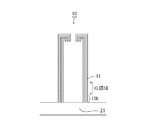
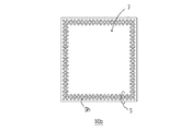
図1は、本発明の実施の形態1におけるフレキシブルプリント配線板シート50を示す平面図である。以下の説明においてフレキシブルプリント配線板およびフレキシブルプリント配線板シートを、それぞれFPCおよびFPCシートと略記する。このFPCシート50の全体は矩形であり、最終的な製品となるFPC10が、複数、配置される製品領域7を取り囲むように外枠部5が設けられている。このFPC10は、支持金属箔と、信号伝達のための配線とが一体化された、磁気ヘッド配線板である。本実施の形態のFPCシート50の最大の特徴は、製品領域7を取り囲む外枠部5全体に欠落部5hである円孔が散在している点にある。外枠部5に設けられた欠落部5hの作用については、この後、順次説明してゆく。
図1において、FPCシート50には、めっきをする際に導通をとるめっきフレーム21が設けられている。図1では、FPC10の配線11は、1本の太線で表示されているが、より詳しくは、図2に示すように、たとえば3本またはそれを超える本数の導線が並行している。配線11は、先端部が屈曲しており、その屈曲部が対向し、対をなすように配置される。配線11から延びてめっきリード部11kが設けられ、このめっきリード部11kは、めっきフレーム21に連結されている。配線11/めっきリード部11k/めっきフレーム21は、図1および図2において、同じ層(高さ、厚み方向位置)である配線層に位置している。
後のめっき処理の説明のために、予め、配線11に対して行う金めっき処理の領域(G領域)を紹介しておく。
(G領域):G領域では、配線11に接続のために金めっき層が形成されている。他の配線層の上には、カバー絶縁層9が位置するが、この接続用の金めっきされた箇所では、カバー絶縁層9は除去されている。また、G領域では、所定領域のステンレス箔が、くりぬかれる。
(Embodiment 1)
FIG. 1 is a plan view showing a flexible printed
In FIG. 1, the
In order to explain the subsequent plating process, a gold plating process region (G region) performed on the
(G region): In the G region, a gold plating layer is formed for connection to the
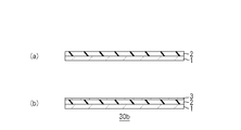
次に、FPCシート50の製造方法を説明する。以後の説明において、完成する前の段階の、FPCシート50の中間製品を、基材シート50bと記す。
図3(a)は、ステンレス箔1上にポリイミドの絶縁層2を形成した状態を示す。ステンレス箔1は、図示しない磁気ヘッドをディスク面から微小浮上させながら弾性支持するために用いられ、所定の弾性率が必要とされる。
次いで、図3(b)に示すように、ポリイミド層2上に、無電解めっきによって導体薄膜3を形成する。導体薄膜3は、電気めっきによって配線11を形成するための下地導電層となる。従来は、そのまま、導体薄膜3上に電気めっきにより銅めっき層の配線等を形成していた。すなわち、中間製品の基材シート(ステンレス箔1/ポリイミド層2/導体薄膜3から形成される矩形シート)に対して、製品領域7の内側に配線11/めっきリード部11kを、また、製品領域7の外縁部、外枠部5の内側にめっきフレームを桟(さん)のように、銅めっき層を形成していた。
この銅めっき処理において、製品領域7の配線11等に電流を流し、銅イオンを銅として析出させる。しかし、上述のように、外枠部5には大面積の導体薄膜3がめっき液中に浸漬されているので、外枠部5にもトータルで大電流が流れる。このため、製品領域7へ流れ込む電流の、外枠部5へ流れ込む電流に対する割合は、小さくなる。また、基材シートが対面する相手側の金属板(陽極)との相対位置の少しのずれによって、孔なし平板の外枠部の辺縁や角部への電流が大きく変化するという外枠部特有の不安定作用もある。このため、製品領域7に流れ込む電流の制御をきめ細かく精度よく行うことが難しいという問題を生じていた。
Next, a method for manufacturing the
FIG. 3A shows a state where a polyimide insulating layer 2 is formed on the stainless steel foil 1. The stainless steel foil 1 is used to elastically support a magnetic head (not shown) while slightly floating from the disk surface, and requires a predetermined elastic modulus.
Next, as shown in FIG. 3B, a conductor
In this copper plating process, a current is passed through the
上記の従来の問題を打開するために、本発明の実施の形態では、基材シート(ステンレス箔1/ポリイミド層2/導体薄膜3から形成される矩形シート)50bの外枠部5の全周にわたって散在するように円孔5hを打ち抜く。図4は、上記基材シート50bの外枠部5の全周に円形の孔を打ち抜いた状態を示す平面図である。これによって、導体薄膜3の上の製品領域7に、銅めっき層11,11k,21を形成する際、外枠部5へ流れ込む電流を大幅に減らし、製品領域7へ流れる電流の制御をきめ細かく高精度にすることができる。この製品領域の電流の制御の精度向上には、孔なし完全平板の外枠部の辺縁や角部における不安定作用が、散在する孔によって外枠部全体にわたって、平均化・希薄化されることも寄与している。また、欠落部5hは外枠部5の中で連結せず、散在するので、外枠部5自体、残っており、所定の強度を有している。このため、ハンドリングのつかみ部、レジストパターン形成時の、レチクルを用いた露光の位置合わせ保持部、などとして機能することができる。
また、めっき処理時に陰極から導電される接続箇所は、めっき電流密度が高いので、外枠部5の導体薄膜(導体層)欠落部5hの割合をそのような陰極導電部において高めるのがよい。その陰極導電箇所から遠ざかるほど導体層欠落部の割合を小さくすることで、外枠部5の強度確保を重視しながら、電流密度分布を平均化することができる。
In order to overcome the above-described conventional problems, in the embodiment of the present invention, the entire circumference of the
Moreover, since the connection location conducted from the cathode during the plating process has a high plating current density, the proportion of the conductor thin film (conductor layer) missing
図5は、銅めっき処理における外枠部5付近を示す断面図である。図5(a)は、製品領域7にレジストパターンR1,R2を形成した段階の、外枠部5付近の断面図である。レジストパターンR1の開口部に、銅めっき層11,11k,21を形成する。
図5(b)は、基材シート50bを銅めっき液中に浸漬して(図9参照)、銅めっき層11,11k,21を形成した状態を示す断面図である。図5(b)の断面図において、外枠部5の導体薄膜3の断面長さは半減しており、面積においても導体薄膜3の大幅な減少が実現している。このとき、図5(b)に示すように、外枠部5の非欠落部の導体薄膜3上には銅めっき層31が形成される。この銅めっき層31は、出荷されるFPCシート50に残り、強度確保に寄与する。外枠部5に設けた欠落部5hによって、銅めっき処理の際、外枠部5に流れ込む電流は大幅に減少する。したがって、銅めっき処理において製品領域7に流れ込む電流の比率が大きく増加する。このため、めっき処理装置の電流値を変えることで、製品領域7に対する電流制御の精度を高めることができようになる。
これにより、簡単な装置で、製品領域の電流値の制御を容易にすることができる。この結果、意図した厚みのめっき層を精度よく均一に形成することが容易になった。従来は、めっき処理装置の電流値を変えても、製品領域の割合が小さかったために、製品領域7に対する電流制御を高精度に行うことができなかった。このため、高精度の厚みのめっき層を均一に得られない場合を生じていた。外枠部の導体薄膜3に欠落部をあける構造では、めっき液を撹拌する場合、通液性が高くなることで、めっき層を均一する効果も含まれる。
図5(c)は、レジストパターンR1,R2を剥離して、めっき処理によって製品領域7に形成された銅めっき層11,11k,21、および外枠部5に形成された銅めっき層31を示す図である。
FIG. 5 is a cross-sectional view showing the vicinity of the
FIG.5 (b) is sectional drawing which shows the state which immersed the
Thereby, it is possible to easily control the current value in the product area with a simple device. As a result, it has become easy to form a plating layer having an intended thickness accurately and uniformly. Conventionally, even if the current value of the plating apparatus is changed, the ratio of the product area is small, so that the current control for the
In FIG. 5C, the resist patterns R1 and R2 are peeled off, and the copper plating layers 11, 11k, and 21 formed in the
図6は、金めっき処理を行うときの基材シート50bの外枠部5付近の断面図である。基材シート50bの製品領域7の中において、表面側では、図6(a)に示すように、G領域はカバー絶縁層(図示せず)に被覆されていない。G領域以外の他の製品領域はカバー絶縁層に被覆されている。ステンレス箔の裏面には図示しないレジストパターンが形成されている。この状態で、金めっき槽に浸漬して金めっき処理を行う(図9参照)。図6(b)は、金めっき層15を形成した後、レジストパターンを剥離した状態を示す図である。金めっき処理の際には、外枠部5は図示しないレジスト膜で被覆されている。
上記の金めっき処理においても、外枠部5に欠落部5hを散在させることで、外枠部5としての空間占有(存在)や強度は実質的に維持し、かつ銅めっき処理と同様に、製品領域7に対するめっき電流の制御を精度よく行うことができる。
FIG. 6 is a cross-sectional view of the vicinity of the
Even in the above gold plating process, the space occupancy (presence) and strength as the
図7は、本実施の形態のFPCシートに対する変形例を示す図である。図1に示すFPCシート50では、外枠部5における欠落部5hは、打ち抜かれた円孔であった。図7の変形例では、外枠部5は格子状であり、四角形の孔が欠落部5hである。図1および図4における円孔を四角孔にする点だけが異なり、後は、製造方法および作用効果については、上述の説明をそのまま用いることができる。
FIG. 7 is a diagram illustrating a modification of the FPC sheet according to the present embodiment. In the
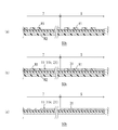
(実施の形態2)
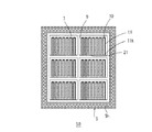
図8は、本発明の実施の形態2におけるフレキシブルプリント配線板シートの製造方法を説明するための図である。本実施の形態における製造方法では、基材シートの外枠部5に貫通孔を設けず、レジストパターンR1によりめっき電流の高精度制御を実現する点に特徴を有する。製造方法は、大略、次のとおりである。
(S1)ステンレス箔1上にポリイミド層2を形成し、そのポリイミド層2上に導体薄膜3を形成する。導体薄膜3は、上述のように、ポリイミドとの密着力が高いニッケルやクロムなどで形成し、無電解めっきやスパッタリングによって形成するのがよい。
(S2)図8(a)に示すように、製品領域7および外枠部5に、同じ機会に、レジストパターンR1を形成する。外枠部5のレジストパターンR1は、たとえば、複数の円形、四角形などが散在するレジスト膜部を有するものとする。
(S3)銅めっき処理を基材シートに施す。レジストパターンR1のレジスト膜部は絶縁体であり、めっき電流が流れないので、実施の形態1における導体層3の欠落部5hと同じ作用を奏する。このため、外枠部5に流れ込む電流を減少させることができる。しかし、このとき図8(b)に示すように、レジストパターン開口部に銅めっき層31が形成される。
(S4)図8(c)に示すように、レジストパターンを除去する。この結果、外枠部5に、上記複数の円形、四角形などの部分が欠落した銅めっき層31が残る。すなわち、出荷時のFPCシートの製品に、銅めっき層31が残る。
(Embodiment 2)
FIG. 8 is a diagram for explaining a method for manufacturing a flexible printed wiring board sheet according to Embodiment 2 of the present invention. The manufacturing method according to the present embodiment is characterized in that a through hole is not provided in the
(S1) A polyimide layer 2 is formed on the stainless steel foil 1, and a conductive
(S2) As shown in FIG. 8A, a resist pattern R1 is formed on the
(S3) A copper plating process is applied to the base material sheet. Since the resist film portion of the resist pattern R1 is an insulator and no plating current flows, the same effect as the missing
(S4) As shown in FIG. 8C, the resist pattern is removed. As a result, the
外枠部に囲まれる製品領域は、配線回路を形成するために、めっき処理の前にレジスパターンを必ず形成する。製品領域のレジストパターンと外枠部のレジストパターンとを同時に形成することで、打ち抜き加工等により外枠部に貫通孔をあける工程を追加する必要はなくなる。すなわち、外枠部のレジストパターンのレジスト膜部にはめっき電流は流れず、導体層の欠落部と同じ作用を奏する。これにより、製造期間の短縮、工数の節約、打ち抜き装置などの不要化を得ることができ、全体的にみて、打ち抜き加工等よりも製造コストを削減することができる。また、欠落部を含まない導体薄膜3、および欠落部を囲む銅めっき層は、外枠部における強度確保に有益である。
また上記の製造方法によれば、実施の形態1と同様に、外枠部5へ流れ込む電流を大幅に減らし、製品領域7へ流れる電流の制御をきめ細かく高精度にすることができる。めっき処理時に陰極から導電される接続箇所は、電流密度が高いので、外枠部5のレジストパターンR1のレジスト膜部の割合をそのような陰極導電部において高めるのがよい。その陰極導電箇所から遠ざかるほどレジスト膜部の割合を小さくすることで、外枠部5の電流密度分布を平均化することができる。
In the product region surrounded by the outer frame portion, a resist pattern is always formed before plating in order to form a wiring circuit. By simultaneously forming the resist pattern in the product region and the resist pattern in the outer frame portion, there is no need to add a step of making a through hole in the outer frame portion by punching or the like. That is, the plating current does not flow in the resist film portion of the resist pattern in the outer frame portion, and has the same effect as the missing portion of the conductor layer. As a result, it is possible to shorten the manufacturing period, save man-hours, and eliminate the need for a punching device. Overall, the manufacturing cost can be reduced as compared with punching or the like. Moreover, the conductor
Further, according to the above manufacturing method, as in the first embodiment, the current flowing into the
(実施の形態3)
図9は、本発明の実施の形態3におけるめっき処理装置70を示す図である。めっき槽77にはめっき液75が投入され、そのめっき液75中に基材シート50bが配置されている。基材シート50bのめっきフレーム21には、図示しない陰極からの配線72が連結されている。また、基材シート50bに対向して、陽極配線71に連結する金属板71aが配置される。金属板71aは、銅めっきの場合は銅板であり、金めっきの場合は金板等が用いられる。図9において、基材シート50bの外枠部は、絶縁体で形成された外枠部マスク81によって被覆されている。図10は、外枠部マスク81を示す斜視図である。外枠部マスク81は、クリップ83によって基材シート50bに取り付けられ、基材シート50bの外枠部を被覆する。
(Embodiment 3)
FIG. 9 is a diagram showing a
図9によれば、基材シート50bの製品領域7のみが、めっき液75に接する。外枠部マスク81は、絶縁体なので、図9に示すように基材シート50bに取り付けられると、外枠部5に流れ込む電流は非常に小さくなる。このため、陰極および陽極間に流れる電流のほとんどは、製品領域7に流れる。この結果、製品領域7に対する電流値の制御を、装置に設けられた電流制御部を用いて、製品領域7の電流値を精度よく制御することができる。これによって、意図したとおりの高精度の厚みで、均一な厚みのめっき層を得ることができる。基材シート50bの外枠部5は、実施の形態1におけるように、導体層3の欠落部5hを設けたものでもよいし、欠落部がない基材シート50bであってもよい。
また、めっき処理時に陰極から導電される箇所(配線72の接続箇所)は、電流密度が高いので、外枠部5のマスク81の被覆率をそのような陰極導電部において高めるのがよい。その陰極導電箇所から遠ざかるほどマスク81の被覆率を小さくすることで、電流密度分布を平均化することができる。
According to FIG. 9, only the
Further, since the current density is high at a portion that is conductive from the cathode during the plating process (connection portion of the wiring 72), the coverage of the
上記において、本発明の実施の形態および実施例について説明を行ったが、上記に開示された本発明の実施の形態および実施例は、あくまで例示であって、本発明の範囲はこれら発明の実施の形態に限定されない。本発明の範囲は、特許請求の範囲の記載によって示され、さらに特許請求の範囲の記載と均等の意味および範囲内でのすべての変更を含むものである。 Although the embodiments and examples of the present invention have been described above, the embodiments and examples of the present invention disclosed above are merely examples, and the scope of the present invention is the implementation of these inventions. It is not limited to the form. The scope of the present invention is indicated by the description of the scope of claims, and further includes meanings equivalent to the description of the scope of claims and all modifications within the scope.
本発明によれば、基材シートのハンドリングの容易さを確保した上で、めっき処理において製品領域への電流値の制御性を高めることができる。この結果、製品領域のめっき層の膜厚精度を向上させ、均一性も確保することができる。 ADVANTAGE OF THE INVENTION According to this invention, the controllability of the electric current value to a product area | region can be improved in a plating process, after ensuring the ease of handling of a base material sheet. As a result, it is possible to improve the film thickness accuracy of the plating layer in the product region and to ensure uniformity.
1 ステンレス箔、2 ポリイミド層(絶縁層)、3 導体薄膜、5 外枠部、5h 外枠部の導体層欠落部、7 製品領域、9 カバー絶縁層、10 フレキシブルプリント配線板(FPC)、11 配線、11k めっきリード部、15 金めっき層、21 めっきフレーム、31 外枠部の銅めっき層、50 FPCシート(フレキシブルプリント配線板シート)、50b 基材シート(中間製品)、70 めっき処理装置、71 陽極配線、71a 金属板(銅板、金板)、72 陰極配線、75 めっき液、77 めっき槽、81 外枠部マスク、83 クリップ。 DESCRIPTION OF SYMBOLS 1 Stainless steel foil, 2 Polyimide layer (insulating layer), 3 Conductor thin film, 5 Outer frame part, 5h Conductor layer missing part of outer frame part, 7 Product area, 9 Cover insulating layer, 10 Flexible printed wiring board (FPC), 11 Wiring, 11k plating lead part, 15 gold plating layer, 21 plating frame, 31 copper plating layer of outer frame part, 50 FPC sheet (flexible printed wiring board sheet), 50b base sheet (intermediate product), 70 plating processing apparatus, 71 anode wiring, 71a metal plate (copper plate, gold plate), 72 cathode wiring, 75 plating solution, 77 plating tank, 81 outer frame mask, 83 clip.
Claims (9)
前記フレキシブルプリント配線板シートは、導体層を含む外枠部と、該外枠部に取り囲まれて前記フレキシブルプリント配線板が形成される製品領域とを有し、
前記フレキシブルプリント配線板シートの中間製品である基材シートに金属層を形成するめっき処理のとき、
前記基材シートの外枠部の導体層へ流れる電流を減少させるために、外枠部電流減少手段を用いることを特徴とする、フレキシブルプリント配線板シートの製造方法。 A method for producing a flexible printed wiring board sheet comprising a plurality of flexible printed wiring boards including a plated metal layer,
The flexible printed wiring board sheet has an outer frame part including a conductor layer, and a product region surrounded by the outer frame part to form the flexible printed wiring board,
At the time of plating treatment to form a metal layer on a base sheet that is an intermediate product of the flexible printed wiring board sheet,
In order to reduce the electric current which flows into the conductor layer of the outer frame part of the said base material sheet, an outer frame part electric current reduction means is used, The manufacturing method of the flexible printed wiring board sheet | seat characterized by the above-mentioned.
前記複数のフレキシブルプリント配線板が位置する製品領域を取り囲むように、導体層を含む外枠部が位置し、
前記外枠部において、(1)前記導体層に欠落部が散在し、非欠落部の前記導体層上に銅めっき層が形成されている、または(2)欠落部を含まない導体層上に銅めっき層を有し、該銅めっき層中に当該銅めっき層が欠落した銅めっき層欠落部が散在することを特徴とする、フレキシブルプリント配線板シート。 A flexible printed wiring board sheet comprising a plurality of flexible printed wiring boards including a plated metal layer,
An outer frame portion including a conductor layer is positioned so as to surround a product region where the plurality of flexible printed wiring boards are located,
In the outer frame portion, (1) missing portions are scattered in the conductor layer, and a copper plating layer is formed on the conductor layers in non-missing portions, or (2) on a conductor layer not including the missing portions. A flexible printed wiring board sheet having a copper plating layer, wherein copper plating layer missing portions where the copper plating layer is missing are scattered in the copper plating layer.
Priority Applications (3)
| Application Number | Priority Date | Filing Date | Title |
|---|---|---|---|
| JP2008262028A JP5190696B2 (en) | 2008-10-08 | 2008-10-08 | Method for producing flexible printed wiring board sheet |
| TW98133782A TWI430723B (en) | 2008-10-08 | 2009-10-06 | Flexible print wiring sheet and method for manufacturing the same |
| CN200910179036.XA CN101720170B (en) | 2008-10-08 | 2009-10-09 | Flexible print wiring plate and its manufacturing method |
Applications Claiming Priority (1)
| Application Number | Priority Date | Filing Date | Title |
|---|---|---|---|
| JP2008262028A JP5190696B2 (en) | 2008-10-08 | 2008-10-08 | Method for producing flexible printed wiring board sheet |
Publications (2)
| Publication Number | Publication Date |
|---|---|
| JP2010093074A true JP2010093074A (en) | 2010-04-22 |
| JP5190696B2 JP5190696B2 (en) | 2013-04-24 |
Family
ID=42255521
Family Applications (1)
| Application Number | Title | Priority Date | Filing Date |
|---|---|---|---|
| JP2008262028A Active JP5190696B2 (en) | 2008-10-08 | 2008-10-08 | Method for producing flexible printed wiring board sheet |
Country Status (3)
| Country | Link |
|---|---|
| JP (1) | JP5190696B2 (en) |
| CN (1) | CN101720170B (en) |
| TW (1) | TWI430723B (en) |
Cited By (4)
| Publication number | Priority date | Publication date | Assignee | Title |
|---|---|---|---|---|
| JP2011214024A (en) * | 2010-03-31 | 2011-10-27 | Dainippon Printing Co Ltd | Circuit board provided with support frame and method for manufacturing the same |
| JP2012033882A (en) * | 2010-07-29 | 2012-02-16 | Samsung Electro-Mechanics Co Ltd | Printed circuit board and manufacturing method thereof |
| CN106102317A (en) * | 2016-06-28 | 2016-11-09 | 广东欧珀移动通信有限公司 | Pcb board and there is its mobile terminal |
| US10548217B1 (en) | 2017-05-16 | 2020-01-28 | Sumitomo Electric Industries, Ltd. | Base material for printed interconnect boards and manufacturing method of printed interconnect boards |
Families Citing this family (3)
| Publication number | Priority date | Publication date | Assignee | Title |
|---|---|---|---|---|
| CN102776551B (en) * | 2012-07-04 | 2015-11-25 | 中国电子科技集团公司第四十一研究所 | A kind of hard microstrip circuit electroplating clamp |
| CN105792509A (en) * | 2014-12-22 | 2016-07-20 | 北大方正集团有限公司 | Manufacturing method of impedance line, impedance line and circuit board |
| CN109496080B (en) * | 2018-10-08 | 2021-04-09 | 江苏长电科技股份有限公司 | Circuit board electroplating process method |
Citations (3)
| Publication number | Priority date | Publication date | Assignee | Title |
|---|---|---|---|---|
| JP2003253496A (en) * | 2002-02-26 | 2003-09-10 | Toppan Printing Co Ltd | Tool and method for electroplating |
| JP2003273498A (en) * | 2002-03-12 | 2003-09-26 | Nitto Denko Corp | Method of manufacturing printed-wiring board |
| JP2007180212A (en) * | 2005-12-27 | 2007-07-12 | Ngk Spark Plug Co Ltd | Manufacturing method and intermediate product of wiring board |
-
2008
- 2008-10-08 JP JP2008262028A patent/JP5190696B2/en active Active
-
2009
- 2009-10-06 TW TW98133782A patent/TWI430723B/en not_active IP Right Cessation
- 2009-10-09 CN CN200910179036.XA patent/CN101720170B/en not_active Expired - Fee Related
Patent Citations (3)
| Publication number | Priority date | Publication date | Assignee | Title |
|---|---|---|---|---|
| JP2003253496A (en) * | 2002-02-26 | 2003-09-10 | Toppan Printing Co Ltd | Tool and method for electroplating |
| JP2003273498A (en) * | 2002-03-12 | 2003-09-26 | Nitto Denko Corp | Method of manufacturing printed-wiring board |
| JP2007180212A (en) * | 2005-12-27 | 2007-07-12 | Ngk Spark Plug Co Ltd | Manufacturing method and intermediate product of wiring board |
Cited By (4)
| Publication number | Priority date | Publication date | Assignee | Title |
|---|---|---|---|---|
| JP2011214024A (en) * | 2010-03-31 | 2011-10-27 | Dainippon Printing Co Ltd | Circuit board provided with support frame and method for manufacturing the same |
| JP2012033882A (en) * | 2010-07-29 | 2012-02-16 | Samsung Electro-Mechanics Co Ltd | Printed circuit board and manufacturing method thereof |
| CN106102317A (en) * | 2016-06-28 | 2016-11-09 | 广东欧珀移动通信有限公司 | Pcb board and there is its mobile terminal |
| US10548217B1 (en) | 2017-05-16 | 2020-01-28 | Sumitomo Electric Industries, Ltd. | Base material for printed interconnect boards and manufacturing method of printed interconnect boards |
Also Published As
| Publication number | Publication date |
|---|---|
| JP5190696B2 (en) | 2013-04-24 |
| TWI430723B (en) | 2014-03-11 |
| CN101720170B (en) | 2014-03-12 |
| TW201021644A (en) | 2010-06-01 |
| CN101720170A (en) | 2010-06-02 |
Similar Documents
| Publication | Publication Date | Title |
|---|---|---|
| JP5190696B2 (en) | Method for producing flexible printed wiring board sheet | |
| CN110551973B (en) | Vapor deposition mask | |
| CN100392725C (en) | Suspension board with circuit and procuding method thereof | |
| CN104781443B (en) | The manufacture method and film formation mask of film formation mask | |
| CN102006716B (en) | Wired circuit board and manufacture method thereof | |
| CN101137272A (en) | Wired circuit board and production method thereof | |
| KR20160029032A (en) | Film-forming mask and method for producing film-forming mask | |
| US9251818B2 (en) | Suspension board with circuits for accurate posture angle adjustment, and method for manufacturing the same | |
| JP2013245392A (en) | Vapor deposition mask and method for manufacturing the same | |
| US20090101399A1 (en) | Suspension board with circuit | |
| JP2016148113A (en) | Method of manufacturing vapor deposition mask, and vapor deposition mask | |
| JP2018195681A (en) | Substrate for printed wiring board and method for manufacturing printed wiring board | |
| JP2008088522A (en) | Pattern-plating method | |
| US9955579B2 (en) | Printed circuit board having reduced loss of electric signal and method of manufacturing the same | |
| US9295160B2 (en) | Printed circuit board and method of manufacturing the same | |
| JP5174785B2 (en) | Printed circuit board | |
| JP2006253574A (en) | Manufacturing method of wiring board | |
| JP2009117600A (en) | Method of manufacturing wiring circuit board with bumps | |
| US20230007783A1 (en) | Method for producing wiring circuit board | |
| JP7203939B2 (en) | Method for manufacturing wired circuit board | |
| JP5766432B2 (en) | Plated metal film substrate, method of manufacturing the same, and semiconductor device | |
| WO2023276510A1 (en) | Flexible printed circuit board and method for manufacturing flexible printed circuit board | |
| JP6027819B2 (en) | Printed circuit board | |
| JPH08272076A (en) | Production of printed wiring board | |
| JP2016199775A (en) | Manufacturing method for vapor deposition mask |
Legal Events
| Date | Code | Title | Description |
|---|---|---|---|
| A625 | Written request for application examination (by other person) |
Free format text: JAPANESE INTERMEDIATE CODE: A625 Effective date: 20110527 |
|
| A977 | Report on retrieval |
Free format text: JAPANESE INTERMEDIATE CODE: A971007 Effective date: 20120517 |
|
| A131 | Notification of reasons for refusal |
Free format text: JAPANESE INTERMEDIATE CODE: A131 Effective date: 20120605 |
|
| A521 | Request for written amendment filed |
Free format text: JAPANESE INTERMEDIATE CODE: A523 Effective date: 20120727 |
|
| TRDD | Decision of grant or rejection written | ||
| A01 | Written decision to grant a patent or to grant a registration (utility model) |
Free format text: JAPANESE INTERMEDIATE CODE: A01 Effective date: 20130107 |
|
| A61 | First payment of annual fees (during grant procedure) |
Free format text: JAPANESE INTERMEDIATE CODE: A61 Effective date: 20130117 |
|
| R150 | Certificate of patent or registration of utility model |
Ref document number: 5190696 Country of ref document: JP Free format text: JAPANESE INTERMEDIATE CODE: R150 Free format text: JAPANESE INTERMEDIATE CODE: R150 |
|
| FPAY | Renewal fee payment (event date is renewal date of database) |
Free format text: PAYMENT UNTIL: 20160208 Year of fee payment: 3 |
|
| R250 | Receipt of annual fees |
Free format text: JAPANESE INTERMEDIATE CODE: R250 |
|
| R250 | Receipt of annual fees |
Free format text: JAPANESE INTERMEDIATE CODE: R250 |
|
| R250 | Receipt of annual fees |
Free format text: JAPANESE INTERMEDIATE CODE: R250 |
|
| R250 | Receipt of annual fees |
Free format text: JAPANESE INTERMEDIATE CODE: R250 |
|
| R250 | Receipt of annual fees |
Free format text: JAPANESE INTERMEDIATE CODE: R250 |
|
| R250 | Receipt of annual fees |
Free format text: JAPANESE INTERMEDIATE CODE: R250 |
|
| R250 | Receipt of annual fees |
Free format text: JAPANESE INTERMEDIATE CODE: R250 |
|
| R250 | Receipt of annual fees |
Free format text: JAPANESE INTERMEDIATE CODE: R250 |
|
| R250 | Receipt of annual fees |
Free format text: JAPANESE INTERMEDIATE CODE: R250 |