JP2010087303A - Thin film transistor substrate for display and method for manufacturing the same - Google Patents
Thin film transistor substrate for display and method for manufacturing the same Download PDFInfo
- Publication number
- JP2010087303A JP2010087303A JP2008255689A JP2008255689A JP2010087303A JP 2010087303 A JP2010087303 A JP 2010087303A JP 2008255689 A JP2008255689 A JP 2008255689A JP 2008255689 A JP2008255689 A JP 2008255689A JP 2010087303 A JP2010087303 A JP 2010087303A
- Authority
- JP
- Japan
- Prior art keywords
- film
- substrate
- conductive pattern
- gate electrode
- semiconductor film
- Prior art date
- Legal status (The legal status is an assumption and is not a legal conclusion. Google has not performed a legal analysis and makes no representation as to the accuracy of the status listed.)
- Granted
Links
Images


Abstract
Description
本発明は、アクティブマトリクス方式のディスプレイ用薄膜トランジスタ基板及びその製造方法に関する。 The present invention relates to a thin film transistor substrate for an active matrix display and a method for manufacturing the same.
アクティブマトリクス駆動型の表示装置において、薄膜トランジスタ(以下、TFTともいう。)は、個々の画素に設けられるスイッチング素子や、表示装置のディスプレイ基板上の周辺回路を構成する回路素子等として利用されている。アクティブマトリクス駆動型の表示装置である液晶ディスプレイパネルや有機ELディスプレイパネルは、携帯電話やPDA等のモバイルディスプレイ用途に使用されることが多く、さらなる軽量化や耐衝撃性を有するTFT基板が望まれている。特に近年においては、ガラス基板の代わりにプラスチック基板を用いたTFT基板が提案されている。 In an active matrix drive display device, a thin film transistor (hereinafter also referred to as TFT) is used as a switching element provided in each pixel, a circuit element constituting a peripheral circuit on a display substrate of the display device, or the like. . Liquid crystal display panels and organic EL display panels, which are display devices driven by an active matrix, are often used for mobile display applications such as mobile phones and PDAs, and TFT substrates having further weight reduction and impact resistance are desired. ing. Particularly in recent years, a TFT substrate using a plastic substrate instead of a glass substrate has been proposed.
こうしたTFT基板のうち、ポリシリコンTFT基板等で用いられるトップゲート型TFT基板においては、パターニングしたゲート電極をシリコン膜へのイオン注入のマスクとして用いる所謂「セルフアラインプロセス」が各種提案されている(例えば特許文献1を参照)。また、トップゲートスタガ型のTFT基板では、シリコン膜を所定パターンにエッチングする際に、パターニングしたゲート電極を利用するセルフアラインプロセスも提案されている。これらのように、トップゲート型のTFT基板でセルフアラインプロセスを適用する場合であって、ゲート電極を形成する前にあらかじめシリコン膜のパターン形成を行わない場合には、ゲート電極をマスクパターンとしているので、ゲート電極の下には必ずシリコン膜が存在した状態となっている。あらかじめシリコン膜のパターニングを行わない理由としては、(a)基板に耐熱性がないためにイオン注入した不純物の活性化を行うのに基板全体を加熱する熱活性化法を利用できず、そのために全面にレーザー光を照射するレーザー活性化法を採用する場合(前者の場合)において、そのレーザー光がシリコン膜がない部分で基板に対してダメージを与える場合や、(b)ゲート電極パターンでシリコン膜をエッチングすることでフォトリソグラフィ工程を1回省略することを目的とした場合(後者の場合)、などが考えられる。 Among such TFT substrates, in a top gate type TFT substrate used for a polysilicon TFT substrate or the like, various so-called “self-alignment processes” using a patterned gate electrode as a mask for ion implantation into a silicon film have been proposed ( For example, see Patent Document 1). In the top gate stagger type TFT substrate, a self-alignment process is also proposed in which a patterned gate electrode is used when a silicon film is etched into a predetermined pattern. As described above, when the self-alignment process is applied to the top gate type TFT substrate and the silicon film pattern is not formed in advance before forming the gate electrode, the gate electrode is used as a mask pattern. Therefore, a silicon film always exists under the gate electrode. The reason for not patterning the silicon film in advance is that (a) the substrate is not heat resistant, so that the thermal activation method of heating the entire substrate cannot be used for activating the ion-implanted impurities. When the laser activation method of irradiating the entire surface with laser light is adopted (in the former case), the laser light damages the substrate in a portion where there is no silicon film, or (b) silicon with a gate electrode pattern A case where the purpose is to omit the photolithography process once by etching the film (in the latter case) can be considered.
ところで、TFT基板をマトリクス型ディスプレイのスイッチング素子として応用する場合、通常、工程数を低減させる目的で、TFTのゲート電極と、そのゲート電極に外部の電圧を供給するための走査線とが共有化されている。こうした態様のTFT基板を製造する際に、上記したセルフアラインプロセスを採用すると、走査線の下に必ずシリコン膜が形成されることになる。 By the way, when a TFT substrate is applied as a switching element of a matrix display, the TFT gate electrode and a scanning line for supplying an external voltage to the gate electrode are usually shared for the purpose of reducing the number of processes. Has been. When the above-described self-alignment process is employed when manufacturing a TFT substrate of such a mode, a silicon film is always formed under the scanning line.
上記態様において、走査線にオン電圧が印加されると、その走査線の下にあるシリコン膜も導通状態となるが、そのシリコン膜はソース−ドレイン領域を介してデータ線や画素電極にも接続されている。そのため、走査線からのオン/オフ電圧をゲート電極に印加することによってソース−ドレイン間に電流が流れたとき、その電流が、ソース−ドレイン領域のシリコン膜から走査線の下にあるシリコン膜に流れ込み、漏洩電流として不具合を引き起こすおそれがある。特に、走査線は多くの画素領域に渡って形成されているので、隣の画素領域に不要な電流が流れたり、画素電極に所望の電圧が供給されなかったりする等の不具合を発生させる可能性がある。 In the above embodiment, when an on-voltage is applied to the scanning line, the silicon film under the scanning line is also in a conductive state, but the silicon film is also connected to the data line and the pixel electrode through the source-drain region. Has been. Therefore, when a current flows between the source and drain by applying an on / off voltage from the scanning line to the gate electrode, the current flows from the silicon film in the source-drain region to the silicon film under the scanning line. Inflow and leakage current may cause problems. In particular, since the scanning line is formed over many pixel areas, there is a possibility that an unnecessary current flows in the adjacent pixel area or a desired voltage is not supplied to the pixel electrode. There is.
本発明は、上記課題を解決するためになされたものであって、その目的は、ソース−ドレイン領域の半導体膜と走査線の下にある半導体膜とが接続されていることに起因して生じる不具合をなくすことができる、アクティブマトリクス方式のディスプレイ用薄膜トランジスタ基板を提供することにある。また、本発明の他の目的は、そうしたディスプレイ用薄膜トランジスタ基板の製造方法を提供することにある。 The present invention has been made to solve the above-described problems, and the object thereof is caused by the connection between the semiconductor film in the source-drain region and the semiconductor film under the scanning line. An object of the present invention is to provide an active matrix type thin film transistor substrate for a display which can eliminate problems. Another object of the present invention is to provide a method for manufacturing such a thin film transistor substrate for a display.
上記課題を解決するための本発明のディスプレイ用薄膜トランジスタ基板は、基板側から、少なくとも、半導体膜、ゲート絶縁膜、ゲート電極の順で設けられた薄膜トランジスタを有するアクティブマトリクス方式のディスプレイ用薄膜トランジスタ基板において、前記ゲート電極をその一部として含む走査線が所定の隙間を隔てて分断された導電性パターンと、該導電性パターンの下に設けられた半導体膜と、前記分断された導電性パターンを接続する配線膜とを有することを特徴とする。 The thin film transistor substrate for display of the present invention for solving the above problems is an active matrix display thin film transistor substrate having thin film transistors provided in this order from the substrate side in the order of a semiconductor film, a gate insulating film, and a gate electrode. A conductive pattern in which a scanning line including the gate electrode as a part thereof is divided at a predetermined gap, and a semiconductor film provided under the conductive pattern are connected to the divided conductive pattern. And a wiring film.
この発明によれば、ゲート電極をその一部として含む走査線が、所定の隙間を隔てて分断された導電性パターンと、その導電性パターンの下に設けられた半導体膜と、分断された導電性パターンを接続する配線膜とを有するので、こうして構成されたTFT基板は、導電性パターンの下には半導体膜が存在するものの、導電性パターンが無いところには半導体膜が存在しない。つまり、導電性パターンの下の半導体膜は、導電性パターンが分断された部位でその導電性パターンと同様に分断されているので、その導電性パターンの下にある半導体膜も分断されている。その結果、走査線からのオン/オフ電圧をゲート電極に印加することによってソース−ドレイン間に電流が流れた場合に、その電流が、ソース−ドレイン領域の半導体膜から導電性パターンの下にある半導体膜に流れ込んだ場合であっても、漏洩電流として隣の画素領域に不要な電流が流れ込んだり、画素電極に所望の電圧が供給されなかったりする等の不具合を発生させることがない。 According to the present invention, the scanning line including the gate electrode as a part thereof is divided by a predetermined gap, the conductive pattern, the semiconductor film provided under the conductive pattern, and the divided conductive pattern. Since the TFT substrate thus configured has a semiconductor film under the conductive pattern, the semiconductor substrate does not exist where there is no conductive pattern. That is, since the semiconductor film under the conductive pattern is divided in the same manner as the conductive pattern at the portion where the conductive pattern is divided, the semiconductor film under the conductive pattern is also divided. As a result, when a current flows between the source and drain by applying an on / off voltage from the scanning line to the gate electrode, the current is below the conductive pattern from the semiconductor film in the source-drain region. Even when the semiconductor film flows into the semiconductor film, an unnecessary current does not flow into the adjacent pixel region as a leakage current or a desired voltage is not supplied to the pixel electrode.
本発明のディスプレイ用薄膜トランジスタ基板の好ましい態様として、前記基板が非耐熱性基板であるように構成する。そうした基板としては例えばプラスチック基板が挙げられる。 As a preferable aspect of the thin film transistor substrate for display of the present invention, the substrate is configured to be a non-heat resistant substrate. An example of such a substrate is a plastic substrate.
基板としてプラスチック基板等の非耐熱性基板を用いる場合において、例えば、半導体膜をパターニングした後に活性化処理を行う工程で薄膜トランジスタ基板を得る場合には、半導体膜が除去された領域の非耐熱性基板に大きな熱的ダメージが生じるため、全ベタの半導体膜に活性化処理を行った後に半導体膜をパターニングすることが望ましい。したがって、本発明のようなトップゲートスタガ型のTFT基板を構成する基板として非耐熱性基板を用いた場合には、ゲート電極をその一部として含む走査線が所定の隙間を隔てて分断された導電性パターンと、その導電性パターンの下に設けられた半導体膜と、その分断された導電性パターンを接続する配線膜とを有するように構成することが特に好ましいのである。 In the case of using a non-heat-resistant substrate such as a plastic substrate as the substrate, for example, when obtaining a thin film transistor substrate in a process of performing an activation process after patterning the semiconductor film, the non-heat-resistant substrate in the region where the semiconductor film is removed Therefore, it is desirable to pattern the semiconductor film after the activation process is performed on the solid semiconductor film. Therefore, when a non-heat-resistant substrate is used as the substrate constituting the top gate stagger type TFT substrate as in the present invention, the scanning line including the gate electrode as a part thereof is divided with a predetermined gap. It is particularly preferable to have a conductive pattern, a semiconductor film provided under the conductive pattern, and a wiring film that connects the divided conductive patterns.
本発明のディスプレイ用薄膜トランジスタ基板の好ましい態様として、前記配線膜が、前記導電性パターン上に直接形成されているように構成してもよいし、前記配線膜が、前記導電性パターン上に形成された絶縁膜のコンタクトホールを介して形成されているように構成してもよい。 As a preferred embodiment of the thin film transistor substrate for display according to the present invention, the wiring film may be formed directly on the conductive pattern, or the wiring film may be formed on the conductive pattern. Alternatively, the insulating film may be formed through a contact hole.
これらの発明によれば、所定の隙間を隔てて分断された導電性パターンを接続する配線膜は、導電性パターン上に直接設けても、導電性パターン上の絶縁膜に形成したコンタクトホールを介して設けてもよく、特にコンタクトホールを有する絶縁膜を形成する場合には、その絶縁膜をゲート電極を覆うように形成する層間絶縁膜と共通のものとすることができるので便利である。 According to these inventions, the wiring film for connecting the conductive patterns separated by a predetermined gap may be provided directly on the conductive pattern, or via the contact hole formed in the insulating film on the conductive pattern. In particular, when an insulating film having a contact hole is formed, it is convenient because the insulating film can be shared with an interlayer insulating film formed so as to cover the gate electrode.
本発明のディスプレイ用薄膜トランジスタ基板の好ましい態様として、前記半導体膜は、前記ゲート電極の下に位置する領域以外の領域がイオン注入されているように構成する。 As a preferable aspect of the thin film transistor substrate for display according to the present invention, the semiconductor film is configured such that a region other than a region located under the gate electrode is ion-implanted.
この発明によれば、半導体膜は、ゲート電極をマスクパターンとした所謂セルフアラインプロセスによりイオン注入されているので、マスクの正確なアライメントを行わなくても位置精度よくイオン注入することができる。 According to the present invention, since the semiconductor film is ion-implanted by a so-called self-alignment process using the gate electrode as a mask pattern, ion implantation can be performed with high positional accuracy without performing accurate mask alignment.
本発明のディスプレイ用薄膜トランジスタ基板の好ましい態様として、前記ゲート電極を覆うように層間絶縁膜が形成されているように構成する。 As a preferred embodiment of the thin film transistor substrate for display according to the present invention, an interlayer insulating film is formed so as to cover the gate electrode.
この発明によれば、ゲート電極を覆うように層間絶縁膜が形成されているので、ゲート電極をソース電極やドレイン電極と絶縁でき、さらにその層間絶縁膜を導電性パターン上に形成する絶縁膜と共通のものとすることができるので便利である。 According to the present invention, since the interlayer insulating film is formed so as to cover the gate electrode, the gate electrode can be insulated from the source electrode and the drain electrode, and further, the insulating film for forming the interlayer insulating film on the conductive pattern; It is convenient because it can be common.
上記課題を解決するための本発明のディスプレイ用薄膜トランジスタ基板の製造方法は、基板側から、少なくとも、半導体膜、ゲート絶縁膜、ゲート電極の順で設けられた薄膜トランジスタを有し、該ゲート電極をその一部として含む走査線が所定の隙間を隔てて分断された導電性パターンと、該導電性パターンの下に設けられた半導体膜と、前記分断された導電性パターンを接続する配線膜とを有する、アクティブマトリクス方式のディスプレイ用薄膜トランジスタ基板の製造方法である。 A method of manufacturing a thin film transistor substrate for a display according to the present invention for solving the above-described problem has a thin film transistor provided in the order of at least a semiconductor film, a gate insulating film, and a gate electrode from the substrate side. The scanning line included as a part has a conductive pattern divided by a predetermined gap, a semiconductor film provided under the conductive pattern, and a wiring film connecting the divided conductive pattern This is a method for manufacturing an active matrix thin film transistor substrate for display.
その第1態様に係る製造方法は、前記基板の全面に半導体膜を形成する工程と、前記半導体膜上にゲート絶縁膜とゲート電極とを形成するとともに、該ゲート電極をその一部として含む走査線を、所定の隙間を隔てて分断した導電性パターンで形成する工程と、前記ゲート電極の上方から前記半導体膜に対してイオン注入処理を行い、前記ゲート電極の下に位置する領域以外の領域にイオン注入する工程と、全面にエネルギービーム照射を行って前記イオン注入した領域を活性化する工程と、前記活性化した領域のうち、ソース拡散領域及びドレイン拡散領域になる部分以外の半導体膜と前記導電性パターンの下にある半導体膜以外の半導体膜とを除去する工程と、前記所定の隙間を隔てて分断された導電性パターンの上に所定パターンの配線膜を形成し、該分断された導電性パターンを接続する工程と、をその順で有することを特徴とする。 The manufacturing method according to the first aspect includes a step of forming a semiconductor film on the entire surface of the substrate, a scan including forming a gate insulating film and a gate electrode on the semiconductor film, and including the gate electrode as a part thereof. A step of forming a line with a conductive pattern divided by a predetermined gap, and a region other than a region located under the gate electrode by performing ion implantation on the semiconductor film from above the gate electrode A step of activating the ion-implanted region by irradiating the entire surface with an energy beam, and a semiconductor film other than a portion of the activated region that becomes a source diffusion region and a drain diffusion region Removing a semiconductor film other than the semiconductor film under the conductive pattern, and disposing a predetermined pattern on the conductive pattern separated by the predetermined gap. Film is formed, and having a step of connecting the divided conductive patterns, at that order.
また、その第2態様に係る製造方法は、前記基板の全面に半導体膜を形成する工程と、前記半導体膜上にゲート絶縁膜とゲート電極とを形成するとともに、該ゲート電極をその一部として含む走査線を、所定の隙間を隔てて分断された導電性パターンで形成する工程と、前記導電性パターンをなすゲート電極をマスクとして、前記ゲート絶縁膜と前記半導体膜とをパターニングする工程と、前記所定の隙間を隔てて分断された導電性パターンの上に所定パターンの配線膜を形成し、該分断された導電性パターンを接続する工程と、をその順で有することを特徴とする。 The manufacturing method according to the second aspect includes a step of forming a semiconductor film on the entire surface of the substrate, a gate insulating film and a gate electrode on the semiconductor film, and the gate electrode as a part thereof. Forming a scanning line including a conductive pattern separated by a predetermined gap, and patterning the gate insulating film and the semiconductor film using the gate electrode forming the conductive pattern as a mask, Forming a wiring film of a predetermined pattern on the conductive pattern divided across the predetermined gap, and connecting the divided conductive pattern in that order.
これら第1,第2態様に係る発明によれば、それぞれの工程を経て製造されたTFT基板は、導電性パターンの下には半導体膜が存在するものの、導電性パターンが無いところには半導体膜が存在しない。つまり、導電性パターンの下の半導体膜は、導電性パターンが分断された部位でその導電性パターンと同様に分断されているので、その導電性パターンの下にある半導体膜も分断されている。その結果、製造されたディスプレイ用薄膜トランジスタ基板においては、走査線からのオン/オフ電圧をゲート電極に印加することによってソース−ドレイン間に電流が流れた場合に、その電流が、ソース−ドレイン領域の半導体膜から導電性パターンの下にある半導体膜に流れ込んだ場合であっても、漏洩電流として隣の画素領域に不要な電流が流れ込んだり、画素電極に所望の電圧が供給されなかったりする等の不具合を発生させることがない。 According to the invention according to the first and second aspects, the TFT substrate manufactured through the respective steps has a semiconductor film under the conductive pattern, but there is no semiconductor film in the place without the conductive pattern. Does not exist. That is, since the semiconductor film under the conductive pattern is divided in the same manner as the conductive pattern at the portion where the conductive pattern is divided, the semiconductor film under the conductive pattern is also divided. As a result, in the manufactured thin film transistor substrate for display, when a current flows between the source and the drain by applying an on / off voltage from the scanning line to the gate electrode, the current flows in the source-drain region. Even when the semiconductor film flows into the semiconductor film under the conductive pattern, an unnecessary current flows into the adjacent pixel region as a leakage current, or a desired voltage is not supplied to the pixel electrode. There is no problem.
本発明のディスプレイ用薄膜トランジスタ基板の製造方法の好ましい態様として、前記基板が非耐熱性基板であるように構成する。 As a preferable aspect of the method for manufacturing a thin film transistor substrate for display according to the present invention, the substrate is configured to be a non-heat resistant substrate.
この発明によれば、半導体膜に活性化処理を行った後にパターニングするように構成されるので、基板として非耐熱性基板を用いた場合であっても、活性化処理によって非耐熱性基板に大きな熱的ダメージを与えない。 According to the present invention, since the semiconductor film is patterned after the activation process, even if a non-heat resistant substrate is used as the substrate, the activation process greatly increases the non-heat resistant substrate. Does not cause thermal damage.
本発明のディスプレイ用薄膜トランジスタ基板の製造方法の好ましい態様として、前記配線膜を、前記導電性パターン上に直接形成するように構成してもよいし、前記配線膜を、前記導電性パターン上にコンタクトホールを有する絶縁膜を形成した後に該絶縁膜上に形成するように構成してもよい。 As a preferred embodiment of the method for manufacturing a thin film transistor substrate for display according to the present invention, the wiring film may be formed directly on the conductive pattern, or the wiring film may be contacted on the conductive pattern. After forming the insulating film having holes, the insulating film may be formed on the insulating film.
これらの発明において、特に導電性パターン上にコンタクトホールを有する絶縁膜を形成した後に該絶縁膜上に形成すれば、その絶縁膜をゲート電極上に形成する層間絶縁膜と共通のものとすることができるので製造上便利である。 In these inventions, in particular, if an insulating film having a contact hole is formed on a conductive pattern and then formed on the insulating film, the insulating film is common with the interlayer insulating film formed on the gate electrode. This is convenient for manufacturing.
本発明のディスプレイ用薄膜トランジスタ基板の製造方法の好ましい態様として、前記ゲート電極を覆うように層間絶縁膜を形成する工程を有するように構成する。 As a preferable aspect of the method for manufacturing a thin film transistor substrate for display according to the present invention, the method includes a step of forming an interlayer insulating film so as to cover the gate electrode.
この発明によれば、ゲート電極を覆うように層間絶縁膜を形成するので、ゲート電極をソース電極やドレイン電極と絶縁でき、さらにその層間絶縁膜を導電性パターン上に形成する絶縁膜と共通のものとすることができるので製造上便利である。 According to the present invention, since the interlayer insulating film is formed so as to cover the gate electrode, the gate electrode can be insulated from the source electrode and the drain electrode, and the interlayer insulating film is formed in common with the insulating film formed on the conductive pattern. Since it can be used, it is convenient in manufacturing.
本発明のディスプレイ用薄膜トランジスタ基板によれば、導電性パターンの下の半導体膜は、導電性パターンが分断された部位でその導電性パターンと同様に分断され、その導電性パターンの下にある半導体膜も分断されているので、走査線からのオン/オフ電圧をゲート電極に印加することによってソース−ドレイン間に電流が流れた場合に、その電流が、ソース−ドレイン領域の半導体膜から導電性パターンの下にある半導体膜に流れ込んだ場合であっても、漏洩電流として隣の画素領域に不要な電流が流れ込んだり、画素電極に所望の電圧が供給されなかったりする等の不具合を発生させることがない。その結果、本発明のディスプレイ用薄膜トランジスタ基板は、前記不具合に基づく不良発生を低減させることができる。 According to the thin film transistor substrate for display of the present invention, the semiconductor film under the conductive pattern is divided in the same manner as the conductive pattern at the portion where the conductive pattern is divided, and the semiconductor film under the conductive pattern Therefore, when a current flows between the source and drain by applying an on / off voltage from the scanning line to the gate electrode, the current flows from the semiconductor film in the source-drain region to the conductive pattern. Even if it flows into the semiconductor film underneath, an unnecessary current may flow into the adjacent pixel region as a leakage current or a desired voltage may not be supplied to the pixel electrode. Absent. As a result, the thin film transistor substrate for display according to the present invention can reduce the occurrence of defects based on the above-mentioned defects.
本発明のディスプレイ用薄膜トランジスタ基板の製造方法によれば、上記のように、漏洩電流として隣の画素領域に不要な電流が流れ込んだり、画素電極に所望の電圧が供給されなかったりする等の不具合を発生させることがないディスプレイ用薄膜トランジスタ基板を製造できるので、前記不具合に基づく不良発生を低減させることができるとともに、製造歩留まりが向上し、さらに例えば液晶ディスプレイ(LCD)や有機発光素子(OLED)等と組み合わせたフレキシブルディスプレイを歩留まりよく低コストで製造できる。また、本発明の製造方法で製造されたTFT基板において、半導体膜は、ゲート電極をマスクパターンとした所謂セルフアラインプロセスによりイオン注入され又はパターニングされるので、マスクの正確なアライメントを行わなくても位置精度よくイオン注入又はパターニングすることができる。 According to the method for manufacturing a thin film transistor substrate for a display of the present invention, as described above, an unnecessary current flows into the adjacent pixel region as a leakage current, or a desired voltage is not supplied to the pixel electrode. Since a thin film transistor substrate for display that is not generated can be manufactured, it is possible to reduce the occurrence of defects based on the above-mentioned defects, improve the manufacturing yield, and for example, a liquid crystal display (LCD), an organic light emitting device (OLED), etc. Combined flexible displays can be manufactured with good yield and low cost. Further, in the TFT substrate manufactured by the manufacturing method of the present invention, the semiconductor film is ion-implanted or patterned by a so-called self-alignment process using the gate electrode as a mask pattern, so that accurate mask alignment is not required. Ion implantation or patterning can be performed with high positional accuracy.
以下、本発明のディスプレイ用薄膜トランジスタ基板及その製造方法について詳細に説明する。なお、本発明は図面の形態や以下の実施形態に限定されるものではない。 Hereinafter, the thin film transistor substrate for display and the manufacturing method thereof according to the present invention will be described in detail. In addition, this invention is not limited to the form of drawing or the following embodiment.
[ディスプレイ用薄膜トランジスタ基板]
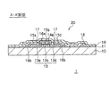
図1は、本発明のディスプレイ用薄膜トランジスタ基板の一例を示す模式平面図であり、図2は、図1に示すTFT基板のA−A’断面図であり、図3は、図1に示すTFT基板のB−B’断面図である。本発明のディスプレイ用薄膜トランジスタ基板1(以下、単に「TFT基板1」ともいう。)は、図1〜図3に示すように、基板10側から、少なくとも、半導体膜13、ゲート絶縁膜14g、ゲート電極15gの順で設けられた薄膜トランジスタ20(以下、単に「TFT20」ともいう。)を有するアクティブマトリクス方式のTFT基板である。そして、本発明は、図1及び図3に示すように、ゲート電極15gをその一部として含む走査線31が所定の隙間Gを隔てて分断された導電性パターン32,32と、その導電性パターン32,32の下に設けられた半導体膜13と、分断された導電性パターン32,32を接続する配線膜33とを有している。
[Thin film transistor substrate for display]
FIG. 1 is a schematic plan view showing an example of a thin film transistor substrate for display according to the present invention, FIG. 2 is a cross-sectional view taken along line AA ′ of the TFT substrate shown in FIG. 1, and FIG. 3 is a TFT shown in FIG. It is BB 'sectional drawing of a board | substrate. The display thin film transistor substrate 1 (hereinafter, also simply referred to as “
より詳しくは、本発明は、図1〜図3に示すように、トップゲート・トップコンタクト構造からなるTFT基板1であり、このTFT基板1に形成されたTFT20は、基板10と、基板10上に必要に応じて設けられたアンダーコート膜11と、アンダーコート膜11上に設けられた半導体膜13(ソース側拡散膜13s、チャネル膜13c及びドレイン側拡散膜13d)と、その半導体膜13上(詳しくは、チャネル膜13c上)に形成されたゲート絶縁膜14gと、ゲート絶縁膜14g上に設けられたゲート電極15gと、ゲート電極15gとゲート絶縁膜14gとを覆うように設けられた層間絶縁膜16aと、ソース側拡散膜13s及びドレイン側拡散膜13dのそれぞれの一部を覆う絶縁膜16bによって形成されたコンタクトホール17と、そのコンタクトホール17を介して設けられたソース電極15s及びドレイン電極15dとを有し、さらのそのTFT20を覆うように設けられた保護膜18とを有している。また、ドレイン電極15dの一端は、画素領域(50A,50B,…)に形成された画素電極19と接続するように設けられている。なお、ゲート電極15gをその一部として含む走査線31は、通常は画素領域(50A,50B,…)毎に分断されている例が多いが、必ずしも画素領域毎でなくてもよい。以下では、説明を分かりやすくするために画素領域毎に分断されている例で説明する。
More specifically, the present invention is a
走査線31の形成部30は、ゲート電極15gをその一部として含み、走査線30が延びる方向に隣接した例えば画素領域(50A,50B,…)毎に、所定の隙間Gを隔てて導電性パターン32が分断されている。導電性パターン32の下には半導体膜13が設けられているが、その半導体膜13も、導電性パターン32が分断されているために同様に分断されている。分断された導電性パターン32上には、その導電性パターン32を電気的に接続するように配線膜33が設けられている。なお、この配線部33は、直接、又は、絶縁膜16cに形成されたコンタクトホール34を介して設けられている。
The
こうした本発明に係るTFT基板1は、導電性パターン32の下には半導体膜13が存在するものの、導電性パターン32が無いところには半導体膜13が存在しない。つまり、導電性パターン32の下の半導体膜13は、導電性パターン32が分断された部位でその導電性パターン32と同様に分断されているので、その導電性パターン32の下にある半導体膜13も分断されている。その結果、走査線31からのオン/オフ電圧をゲート電極15gに印加することによってソース−ドレイン間に電流が流れた場合に、その電流が、ソース−ドレイン領域の半導体膜(ソース側拡散膜13s,ドレイン側拡散膜13d)から導電性パターン32の下にある半導体膜13に流れ込んだ場合であっても、漏洩電流として隣の画素領域に不要な電流が流れ込んだり、画素電極19に所望の電圧が供給されなかったりする等の不具合を発生させることがない。
In the
さらに、本発明のTFT基板1においては、基板10としてプラスチック基板等の非耐熱性基板を用いる場合に、半導体膜13をパターニングした後にその全面にエネルギービーム照射25による活性化処理を行う工程を経てTFT基板1を製造するような場合には、半導体膜13が除去された領域の非耐熱性基板に大きな熱的ダメージが生じるため、全ベタの半導体膜13の全面にエネルギービーム照射を行った後に半導体膜13をパターニングする工程を経てTFT基板1を製造することが望ましい(本発明の第1態様に係る製造方法)。したがって、本発明のようなトップゲートスタガ型のTFT基板1を構成する基板10として非耐熱性基板を用いた場合には、ゲート電極15gをその一部として含む走査線31が所定の隙間Gを隔てて分断された導電性パターン32と、その導電性パターン32の下に設けられた半導体膜13と、その分断された導電性パターン32を接続する配線膜33とを有するように構成することが特に好ましい。
Furthermore, in the
また、本発明においては、ゲート電極15gとゲート絶縁膜14gとを覆うように層間絶縁膜16aが形成されているので、ゲート電極15gをソース電極15sやドレイン電極15dと絶縁でき、さらにその層間絶縁膜16aを導電性パターン32上に形成する絶縁膜16cと共通のものとすることができるので便利である。
In the present invention, since the
[製造方法]
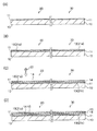
本発明のTFT基板の製造方法は、上記本発明のTFT基板1を製造する方法である。そして、本発明の第1態様に係る製造方法は、基板10の全面に半導体膜13(例えば非晶質シリコン膜21a)を形成する工程と、その半導体膜13(例えば非晶質シリコン膜21a)上にゲート絶縁膜14gとゲート電極15gとを形成するとともに、ゲート電極15gをその一部として含む走査線31を、所定の隙間Gを隔てて分断した導電性ターン32で形成する工程と、ゲート電極15gの上方から半導体膜13に対してイオン注入処理を行い、ゲート電極15gの下に位置する領域以外の領域の半導体膜13にイオン注入する工程と、全面にエネルギービーム照射25を行って前記イオン注入した領域を活性化する工程と、活性化した領域のうち、ソース側拡散膜14s及びドレイン側拡散膜14dになる部分以外の半導体膜13と導電性パターン32の下にある半導体膜以外の半導体膜13とを除去する工程と、所定の隙間Gを隔てて分断された導電性パターン32の上に所定パターンの配線膜32を形成し、分断された導電性パターン32を接続する工程と、をその順で有している。
[Production method]
The manufacturing method of the TFT substrate of the present invention is a method of manufacturing the
また、本発明の第2態様に係る製造方法は、基板10の全面に半導体膜13を形成する工程と、半導体膜13上にゲート絶縁膜14gとゲート電極15gとを形成するとともに、ゲート電極15gをその一部として含む走査線31を、所定の隙間Gを隔てて分断された導電性パターン32で形成する工程と、導電性パターン32をなすゲート電極15gをマスクとして、ゲート絶縁膜14gと半導体膜13とをパターニングする工程と、所定の隙間Gを隔てて分断された導電性パターン32の上に所定パターンの配線膜32を形成し、分断された導電性パターン32を接続する工程と、をその順で有している。
Further, in the manufacturing method according to the second aspect of the present invention, the step of forming the
これら第1,第2態様に係る製造方法は、ゲート電極を形成する前にあらかじめ半導体膜のパターン形成を行わない場合であるが、それぞれの工程を経て製造されたTFT基板1は、導電性パターン32の下には半導体膜13が存在するものの導電性パターン32が無いところには半導体膜13が存在しない。つまり、導電性パターン32の下の半導体膜13は、導電性パターン32が分断された部位でその導電性パターン32と同様に分断されているので、その導電性パターン32の下にある半導体膜13も分断されている。その結果、製造されたディスプレイ用TFT基板1においては、走査線31からのオン/オフ電圧をゲート電極15gに印加することによってソース−ドレイン間に電流が流れた場合に、その電流が、ソース−ドレイン領域の半導体膜13から導電性パターン32の下にある半導体膜13に流れ込んだ場合であっても、漏洩電流として隣の画素領域に不要な電流が流れ込んだり、画素電極に所望の電圧が供給されなかったりする等の不具合を発生させることがないという利点がある。
These manufacturing methods according to the first and second embodiments are cases where the semiconductor film pattern is not formed in advance before forming the gate electrode, but the
特に第1態様に係る製造方法によれば、ゲート電極15gの上方から半導体膜13に対してイオン注入処理を行い、そのゲート電極15gの下に位置する領域以外の領域にイオン注入する工程と、全面にエネルギービーム照射を行ってイオン注入した領域を活性化する工程とを有するので、こうした工程を経て製造されたTFT基板1において、半導体膜13は、ゲート電極15gをマスクパターンとした所謂セルフアラインプロセスによりイオン注入され、その結果、マスクの正確なアライメントを行わなくても位置精度よくイオン注入することができる。また、基板10に耐熱性がないためにイオン注入した不純物の活性化を行うのに基板全体を加熱する熱活性化法を利用できず、そのために全面にレーザー光を照射するレーザー活性化法を採用する場合には、そのレーザー光が半導体膜13がない部分で基板10に対してダメージを与えることがないので、この第1態様に係る発明が好ましく適用される。
In particular, according to the manufacturing method according to the first aspect, an ion implantation process is performed on the
また、第2態様に係る製造方法によれば、導電性パターン32をなすゲート電極15gをマスクとしてゲート絶縁膜14gと半導体膜31とをパターニングする工程を有するので、フォトリソグラフィ工程の回数を上記第1態様の場合に比べて省略することができる。
In addition, according to the manufacturing method according to the second aspect, since the
本発明は、こうした製造工程により、導電性パターン32の下にある半導体膜13も導電性パターン32と同様に分断している。
In the present invention, the
以下においては、図1〜図3に示したTFT基板1を例にして、TFT基板1の構造と製造方法を、図4〜図6に示した第1態様に係る製造方法により説明する。なお、本発明のTFT基板及びその製造方法において、特にその平面形態は図示の例に限定されず、本発明の特徴を有する範囲でその平面配置が変更されたものであってもよい。
Hereinafter, taking the
先ず、基板10を準備する。基板10は、TFT基板1の支持基板をなすものであり、有機基板であっても無機基板であってもよい。有機基板としては、例えば、ポリエーテルサルホン(PES)、ポリエチレンナフタレート(PEN)、ポリアミド、ポリブチレンテレフタレート、ポリエチレンテレフタレート、ポリフェニレンサルファイド、ポリエーテルエーテルケトン、液晶ポリマー、フッ素樹脂、ポリカーボネート、ポリノルボルネン系樹脂、ポリサルホン、ポリアリレート、ポリアミドイミド、ポリエーテルイミド、又は熱可塑性ポリイミド等からなる有機基板、又はそれらの複合基板を挙げることができる。こうした有機基板は、剛性を有するものであってもよいし、厚さが5μm以上300μm以下程度の薄いフレキシブルなフィルム状のものであってもよい。フレキシブルな有機基板(プラスチック基板ともいう。)の使用は、TFT基板1をフレキシブル基板とすることができるので、フィルムディスプレイ等に適用できる。
First, the
また、無機基板としては、例えば、ガラス基板、シリコン基板、セラミックス基板等を挙げることができる。ガラス基板としては、厚さが0.05mm以上3.0mm以下程度の液晶ディスプレイ用途のガラス基板であってもよい。 Moreover, as an inorganic substrate, a glass substrate, a silicon substrate, a ceramic substrate etc. can be mentioned, for example. The glass substrate may be a glass substrate for liquid crystal displays having a thickness of about 0.05 mm to 3.0 mm.
本発明では、後述のように、基板10が、半導体膜13への活性化処理(エネルギービーム照射25)によってダメージを受ける非耐熱性基板である場合に特に効果的である。非耐熱性基板としては、通常は、有機基板(プラスチック基板等)が挙げられるが、無機基板であっても活性化処理(エネルギービーム照射25)等の熱負荷によってダメージを受ける限りにおいては非耐熱基板ということができる。
As will be described later, the present invention is particularly effective when the
次に、図4(A)に示すように、準備された基板10上に必要に応じてアンダーコート膜11を形成する。アンダーコート膜11は、必須の膜ではなく、例えば、(i)半導体膜13と基板10との密着性を向上させるための密着膜として、又は、(ii)後工程で形成した膜が有する応力を緩和させる応力緩衝膜として、又は、(iii)基板10内の不純物がTFTに侵入するのを防ぐバリア膜として、又は、(iv)非耐熱性基板を用いた場合において後工程で加わる熱に対する熱緩衝膜として、設けることができる。したがって、密着性がよかったり、応力の影響がなかったり、バリア性を考慮する必要がなかったり、非耐熱性基板を用いない場合には設ける必要はない。
Next, as shown in FIG. 4A, an
例えば密着膜としてアンダーコート膜11を設ける場合、そのアンダーコート膜11はTFT20が形成される部分と走査線31が形成される部分には少なくとも形成されている必要があるが、それ以外の領域には形成されていてもいなくてもよく、基板10の全面に形成されていてもよい。なお、図4(A)に示す例では、アンダーコート膜11を全面に形成している。
For example, when the
アンダーコート膜11は、上記(i)〜(iv)の目的に応じ、クロム、チタン、アルミニウム、ケイ素、酸化クロム、酸化チタン、酸化アルミニウム、酸化ケイ素、窒化ケイ素、及び酸窒化ケイ素の群から選択されるいずれかの材料で形成される。例えば密着膜として用いる場合には、クロム、チタン、アルミニウム、又はケイ素等からなる金属系の無機膜が好ましく用いられ、応力緩和膜や熱緩衝膜として用いる場合には、酸化クロム、酸化チタン、酸化アルミニウム、酸化ケイ素、窒化ケイ素、又は酸窒化ケイ素等からなる化合物膜が好ましく用いられ、バリア膜として用いる場合には、酸化ケイ素又は酸窒化ケイ素等からなる化合物膜が好ましく用いられる。これらの膜は、その目的に応じて、単層で設けてもよいし、2層以上を積層してもよい。
The
アンダーコート膜11を密着膜として設ける場合の厚さは、膜を構成する材質によってその範囲は若干異なるが、通常1nm以上200nm以下の範囲内であることが好ましく、3nm以上50nm以下の範囲内であることがより好ましい。なお、クロム、チタン、アルミニウム、又はケイ素からなる金属系の無機膜をアンダーコート膜11として形成する場合には、3nm以上10nm以下の範囲内であることがより好ましく、酸化クロム、酸化チタン、酸化アルミニウム、酸化ケイ素、窒化ケイ素、酸窒化ケイ素、酸化アルミニウム、窒化アルミニウム、又は酸窒化アルミニウムからなる化合物系の無機膜をアンダーコート膜11として形成する場合には、5nm以上50nm以下の範囲内であることがより好ましい。一方、アンダーコート膜11を応力からなる化合物膜、バリア膜又は熱緩衝膜として設ける場合の厚さも実際に形成する膜の材質によってその範囲は若干異なるが、その厚さとしては、通常、100nm以上1000nm以下の範囲内であることが好ましく、成膜時間の点からは100nm以上500nm以下の範囲内であることがより好ましい。
The thickness when the
アンダーコート膜11は、DCスパッタリング法、RFマグネトロンスパッタリング法、プラズマCVD法等の各種の方法で形成することができるが、実際には、膜を構成する材質に応じた好ましい方法が採用される。通常は、DCスパッタリング法やRFマグネトロンスパッタリング法等が好ましく用いられる。
The
次に、図4(B)に示すように、基板10上(アンダーコート膜11が設けられている場合には、その上)に半導体膜13を形成する。半導体膜13としては、シリコン、酸化亜鉛、InGaZnO等の各種の半導体膜を挙げることができる。以下においては、代表的な半導体膜13としてシリコン膜を例にして説明するが、通常は非晶質シリコン膜21aが設けられるので、以下においては特に断らない限り「非晶質シリコン膜21a」として説明する。なお、非晶質シリコン膜21aと多結晶シリコン膜21pの両方を特定せずに総称する場合には「半導体膜13」として説明する。
Next, as shown in FIG. 4B, a
非晶質シリコン膜21aの厚さは特に限定されず、通常、20nm以上200nm以下の範囲内である。この非晶質シリコン膜21aは、RFマグネトロンスパッタリング法やCVD法等の各種の方法で成膜可能である。例えばRFマグネトロンスパッタリング法で非晶質シリコン膜21aを成膜する場合には、例えば、成膜温度:室温、成膜圧力:0.2Pa、ガス:アルゴンの成膜条件で例えば厚さ50nmの厚さで成膜できる。なお、CVD法で非晶質シリコン膜21aを成膜する場合も25℃程度の成膜温度で成膜可能であるが、原料ガスとしてSiH4が使用されるので、成膜後に約450℃の脱水素処理(真空中で1時間程度)が必要となる。
The thickness of the
次に、図4(C)(D)に示すように、非晶質シリコン膜21a上の全面に、ゲート絶縁膜14gと導電性パターン32の下に設けられた絶縁膜14とを形成するための絶縁膜14(図4(C))と、ゲート電極15g及び導電性パターン32を形成するための金属膜15(図4(D))とをその順で形成する。
Next, as shown in FIGS. 4C and 4D, the
絶縁膜14としては、通常、酸化ケイ素膜が用いられ、その厚さは、通常、15nm以上300nm以下の範囲である。この絶縁膜14は、例えばRFマグネトロンスパッタリング等で形成される。絶縁膜14の形成方法としては、例えばRFマグネトロンスパッタリング装置を用い、8インチのSiO2ターゲットに投入電力:1.0kW(=3W/cm2)、圧力:1.0Pa、ガス:アルゴン+O2(50%)の成膜条件で厚さ約100nmの酸化ケイ素膜を形成する。
As the insulating
また、絶縁膜14上に形成する金属膜15としては、通常、アルミニウム(Al)、銅(Cu)、その他の導電性材料が用いられ、その厚さは、通常、30nm以上300nm以下の範囲である。この金属膜15は、真空蒸着や、スパッタリング等の成膜プロセスにより形成される。
In addition, as the
この工程のサブ工程として、非晶質シリコン膜21a上の全面に、(1)絶縁膜14を形成する前、又は(2)絶縁膜14を形成した後で金属膜15を形成するまでの間、のいずれかのタイミングで、絶縁膜14の上方からレーザー照射22を行って非晶質シリコン膜21aを多結晶化し、低抵抗の多結晶シリコン膜21pに変化させる結晶化工程を付加してもよい。このときのレーザー照射22は、非晶質シリコン膜21aを多結晶化させて多結晶シリコン膜21pにする結晶化手段であり、XeClエキシマレーザー、CW(Continuous Wave)レーザー等の種々のレーザーを用いて行うことができる。例えば、波長308nmのXeClエキシマレーザーを用いて結晶化を行う場合には、一例として、パルス幅:30nsec(FWHM(半値幅):full width at half-maximum)、エネルギー密度:200〜300mJ/cm2、室温の条件下で行うことができる。なお、このサブ工程は無くてもよい。
As a sub-step of this step, (1) before forming the insulating
上記(1)のサブ工程Aでは、絶縁膜14を形成する前にレーザー照射22を行うが、基板10上の全面に非晶質シリコン膜21aが形成されているので、その非晶質シリコン膜21aがレーザー吸収膜となって基材10にレーザー照射22に基づく熱ダメージを与えないという利点がある。こうした非晶質シリコン膜21aが全面に形成された状態でのレーザー照射22は、特に基板10がプラスチック基板等の非耐熱性基板である場合に好ましい。
In the sub-step A of (1) above, the
また、上記(2)のサブ工程Bでは、図4(C)に示すように、絶縁膜14を形成した後、金属膜15を形成するまでの間にレーザー照射22を行うが、基板10上の全面に非晶質シリコン膜21aと絶縁膜14が形成されているので、その非晶質シリコン膜21aがレーザー吸収膜となって基材10にレーザー照射22に基づく熱ダメージを与えないという利点がある。こうした非晶質シリコン膜21aと絶縁膜14とが全面に形成された状態でのレーザー照射22は、特に基板10がプラスチック基板等の非耐熱性基板である場合に好ましい。さらに、このサブ工程Bでは、非晶質シリコン膜21aを形成した後に絶縁膜14を連続して形成するので、非晶質シリコン膜21aの表面がレーザー照射時の大気雰囲気に曝されることがなく、その結果、非晶質シリコン膜21aと絶縁膜14との界面での酸化や欠陥の発生を抑制でき、その後にゲート絶縁膜14gとなった後においてはTFTとしての電気特性に優れたものとなる。
Further, in the sub-step B of (2) above, as shown in FIG. 4C,
以下の工程においては、結晶化工程であるサブ工程Bを経たものについて説明する。 In the following process, what passed through sub process B which is a crystallization process is explained.
次に、図5(E)に示すように、ゲート電極15gをその一部として含む走査線31を、所定の隙間Gを隔てて分断した導電性ターン32で形成する。
Next, as shown in FIG. 5E, the
この工程では、先ず、絶縁膜14と金属膜15とをパターニングする。パターニングは、感光性ポリマー等からなるレジスト膜を用いた通常のフォトリソグラフィで行われる。具体的には、金属膜15上にマスク層となるレジスト膜を形成した後、フォトマスクを用いたフォトリソグラフィにより露光・現像して所定パターンのマスク層を形成し、その後、マスク層で覆われていない露出部分の金属膜15を例えば燐酸溶液でエッチング除去してゲート電極15g及び導電性パターン32を形成する。引き続いて、マスク層を例えば有機溶液でエッチング除去した後、所定のパターンで形成されたゲート電極15g及び導電性パターン32をマスクとした所謂セルフアラインプロセスにより、露出した絶縁膜14を例えばフッ酸溶液でエッチング除去してゲート絶縁膜14gを形成するとともに、導電性パターン32の下に設けられた絶縁膜14を形成する。こうしたセルフアラインプロセスにより、ゲート電極15gと導電性パターン32の下には、それぞれ同じ形状にパターニングされたゲート絶縁膜14gと絶縁膜14がある。
In this step, first, the insulating
金属膜15上に形成したマスク層のパターンは、ゲート電極15gをその一部として含む走査線31の平面視パターン(図1を参照)と同じパターンである。そして、そのパターンをマスクとしたフォトリソグラフィにより、ゲート電極15gをその一部として含む走査線31を、例えば画素領域(50A,50B,…等)毎に所定の隙間Gを隔てて分断した導電性ターン32で形成することができる。なお、走査線31は、ゲート電極15gの幅と同じ幅で各画素領域を横切るように連続して形成されているのが一般的であるが、本発明においては、導電性パターン32は図1に示すように所定の隙間Gを隔てて分断されている。隙間Gの長さは特に限定されず、例えば0.2μm以上1000μm以下の範囲で設定できる。導電性パターン32の形状も特に限定されず、例えば、走査線31のライン幅よりも大きな四角形(図1参照)や、丸形のパターンとすることができる。
The pattern of the mask layer formed on the
次に、図5(F)に示すように、ゲート電極15gの上方から半導体膜13(非晶質シリコン膜21aに対し、又は、図4(C)に示すレーザー照射した場合には多結晶シリコン膜21p)に対してイオン注入処理を行い、ゲート電極15gの下に位置する領域以外の領域にイオン注入24する。イオン注入24は、例えば、リン(P)を注入電圧:10keV、室温下で、5×10¹⁴イオン/cm2〜2×1015イオン/cm2のドーズ量となるように注入する。注入元素としては、リンの他、ホウ素、アンチモン、ヒ素等、半導体膜にイオン注入できる公知のものを任意に選択して注入してもよい。
Next, as shown in FIG. 5 (F), when the semiconductor film 13 (
本発明において、このイオン注入24は、ゲート電極15gをマスクとした所謂セルフアラインプロセスとして行われる。したがって、この工程により、ゲート電極15gの下に位置してチャネル膜13cとなる領域以外の領域(ソース側拡散膜13sになる領域と、ドレイン側拡散膜13dになる領域)がイオン注入される。イオン注入される半導体膜が非晶質シリコン膜21aである場合には、イオン注入によっても非晶質シリコン膜21aは非晶質相をそのまま維持するが、イオン注入される半導体膜がレーザー照射によって多結晶シリコン膜21pになっている場合には、イオン注入によってその多結晶シリコン膜21pは非晶質シリコン膜21aに変化する。いずれの場合も、イオン注入された部分は非晶質シリコン膜21aになっている。したがって、この工程においては、ゲート電極15gの下に位置する領域以外の半導体膜(チャネル膜13c)に対し、そのゲート電極15gをマスクパターンとする所謂セルフアラインプロセスによりイオン注入するので、マスクの正確なアライメントを行わなくても位置精度よくイオン注入することができる。
In the present invention, the ion implantation 24 is performed as a so-called self-alignment process using the
次に、図5(G)に示すように、全面にエネルギービーム照射25を行って前記イオン注入した領域を活性化する。この工程は、前記セルフアラインプロセスによってイオン注入した領域(すなわち、ゲート電極15gの下に位置するチャネル膜13cとなる領域以外の領域)をエネルギービーム照射25して活性化させ、ソース側拡散膜13sとなる領域及びドレイン側拡散膜13dとなる領域を形成する。この活性化工程では、イオン注入された非晶質シリコン膜21aが再結晶化して多結晶シリコン膜21pに変化するとともに、ゲート電極15gの下に位置してイオン注入されずにチャネル膜13cとなる非晶質シリコン膜21aも再結晶化して多結晶シリコン膜21pに変化する。ここで、エネルギービーム照射25とは、レーザー等のエネルギービームを照射して再結晶化する処理であり、必ずしもレーザーを用いるものでなくてもよい。
Next, as shown in FIG. 5G,
エネルギービーム照射25として、XeClエキシマレーザー、CW(Continuous Wave)レーザー等の種々のレーザーを用いて行うことができる。例えば、波長308nmのXeClエキシマレーザーを用いて結晶化を行う場合には、一例として、パルス幅:30nsec(FWHM(半値幅):full width at half-maximum)、エネルギー密度:150〜250mJ/cm2、室温の条件下で行うことができる。このとき、エネルギービーム照射25をライン状のレーザー照射で行うことにより、TFT基板の全面を効率的に活性化することができる。
As the
次に、図5(H)に示すように、活性化した領域のうち、ソース側拡散膜14s及びドレイン側拡散膜14dになる部分以外の多結晶シリコン膜21pを除去してアイランド化し、多結晶シリコン半導体膜(13s,13c,13d)とするとともに、導電性パターン32の下にある半導体膜以外の不要な多結晶シリコン膜21pを除去する。アイランド化による多結晶シリコン半導体膜(13s,13c,13d)の形成と不要な多結晶シリコン膜21pの除去は、フォトリソグラフィによってエッチング除去して行うが、通常、残す部分の上のみにマスク層を形成した後にドライエッチングして行われる。このときのエッチングガスとしては、SF6等を用いることができる。
Next, as shown in FIG. 5H, in the activated region, the
上記アイランド化による多結晶シリコン半導体膜と多結晶シリコン半導体膜(13s,13c,13d)の形成と不要な多結晶シリコン膜21pの除去を行った後においては、通常、多結晶シリコン半導体膜(13s,13c,13d)の欠陥を低減処理するための酸素プラズマによる欠陥処理が施される。酸素プラズマ処理は、一例として、RF100W、1Torr(133Pa)、150℃の条件下で行われ、その後においては、120℃の条件下での乾燥処理が施される。
After the formation of the polycrystalline silicon semiconductor film and the polycrystalline silicon semiconductor film (13s, 13c, 13d) by the island formation and the removal of the unnecessary
本発明においては、半導体膜に対してその全面にエネルギービーム照射25を行った後にその半導体膜をパターニングしてアイランド化するので、基板10として非耐熱性基板を用いた場合であっても、エネルギービーム照射25によって非耐熱性基板に大きな熱的ダメージを与えない。
In the present invention, the semiconductor film is patterned to form an island after the
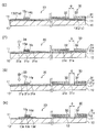
次に、図6(I)に示すように、ゲート電極15gと多結晶シリコン半導体膜(13s,13d)とを含む全面に絶縁膜16を形成した後に、その絶縁膜16をパターニングしてゲート電極15gを覆うように層間絶縁膜16aを形成する。なお、図6(I)に示すコンタクトホール17は、層間絶縁膜16aを形成するのと同時に形成してもよいし、層間絶縁膜16aを形成した後の別工程で絶縁膜を形成した後にその絶縁膜を選択的にパターニングして形成してもよい。これらのパターニングは、例えば、レジスト等のマスク層を形成した後、フォトマスクを用いたレジストプロセスにより露光・現像することによって行うことができる。コンタクトホール17を形成するための絶縁膜16bは、例えば2%HF溶液を用いてウエットエッチングしてパターン形成でき、その後、レジスト剥離処理やプラズマアッシングによりマスク層を除去する。この工程では、層間絶縁膜16aにより、ゲート電極15gをソース電極15sやドレイン電極15dと絶縁できる。
Next, as shown in FIG. 6I, after the insulating film 16 is formed on the entire surface including the
なお、図6(I)中の走査線31の形成部30のコンタクトホール34も、層間絶縁膜16aと共通のものとして同時に形成してもよいし、コンタクトホール17を形成するための絶縁膜16bと共通のものとして同時に形成してもよいし、層間絶縁膜16aや絶縁膜16bを形成した後の別工程で絶縁膜16cを形成した後にその絶縁膜16cを選択的にパターニングして形成してもよい。上記同様、このコンタクトホール34を形成するための絶縁膜16cも、例えば2%HF溶液を用いてウエットエッチングしてパターン形成でき、その後、レジスト剥離処理やプラズマアッシングによりマスク層を除去することができる。
Note that the
次に、図6(J)に示すように、高圧水蒸気28による処理を行って多結晶シリコン半導体膜13(13s,13c,13d)の半導体膜中の欠陥及び界面欠陥をターミネートする。例えば、0.5MPa・150℃程度の高圧水蒸気処理により、半導体表面のダングリングボンドを終端し、多結晶シリコン半導体膜13(13s,13c,13d)とゲート絶縁膜14gとの界面のリークパスをなくす方法がとられる。
Next, as shown in FIG. 6 (J), treatment with high-
次に、図6(K)に示すように、全面に例えば厚さ50nm以上のアルミニウム(Al)膜等を蒸着した後、ウエットエッチングによりパターニングして、ソース電極15s及びドレイン電極15dを形成する。電極材料は、アルミニウムの他、銅(Cu)、その他の導電性材料であってもよく、スパッタリング等の他の成膜プロセスにより形成してもよい。このとき、ドレイン電極15dは、図1及び図2に示すように、画素電極19に接続するように形成される。
Next, as shown in FIG. 6K, an aluminum (Al) film having a thickness of, for example, 50 nm or more is deposited on the entire surface, and then patterned by wet etching to form the
この工程においては、同時に、所定の隙間Gを隔てて分断された導電性パターン32の上に所定パターンの配線膜33を形成し、分断された導電性パターン32を接続する工程を兼ねることができる。すなわち、配線膜33は、この工程でソース電極15s及びドレイン電極15dを形成するのと同時に、導電性パターン32上に直接形成してもよい。また、導電性パターン32上にコンタクトホール34を有する絶縁膜16cを形成した場合においては、そのコンタクトホール34を介して配線膜33を形成してもよい。こうして形成した配線膜33は、所定の隙間Gを隔てて分断された導電性パターン32を接続する。
In this step, simultaneously, a
なお、画素電極19は、図4〜図6で示す工程中のいずれの工程で形成してもよいが、一例としては、図6(K)に示す工程でソース電極15sとドレイン電極15dを形成する前に形成してもよいし、後述する図6(L)に示す工程で保護層18を形成する前に形成してもよい。画素電極19の形成材料としては、例えばITO、IZO等を挙げることができ、その形成方法としては、例えばRFマグネトロンスパッタリング等で形成することができる。
Note that the
次に、図6(L)に示すように、TFT20や走査線31の形成部30を覆う保護膜18を形成する。保護膜18としては、酸化ケイ素膜を好ましく挙げることができる。保護膜18は、例えばRFマグネトロンスパッタリングにより、約20nm程度の厚さで形成することが好ましい。なお、画素電極19上には保護膜19は形成しない。こうして図2及び図3に示す実施形態からなるTFT基板1が製造される。
Next, as shown in FIG. 6L, a
図4〜図6に例示した工程は、図1〜図3に示すTFT基板1の第1態様に係る製造方法を適用した製造例であるが、本発明のTFT基板1は、図示の工程例に限定されず、種々の変形態様で製造することができ、また、第2態様に係る製造方法を適用することもできる。
The process illustrated in FIGS. 4 to 6 is a manufacturing example to which the manufacturing method according to the first embodiment of the
ここで、本発明の第2態様に係る製造方法について、上記した第1態様に係る製造方法と異なる点のみについて説明する。第2態様に係る製造方法は、上記のように、基板10の全面に半導体膜13を形成する工程と、半導体膜13上にゲート絶縁膜14gとゲート電極15gとを形成するとともに、ゲート電極15gをその一部として含む走査線31を、所定の隙間Gを隔てて分断された導電性パターン32で形成する工程と、導電性パターン32をなすゲート電極15gをマスクとして、ゲート絶縁膜14gと半導体膜13とをパターニングする工程と、所定の隙間Gを隔てて分断された導電性パターン32の上に所定パターンの配線膜32を形成し、分断された導電性パターン32を接続する工程と、をその順で有している。
Here, the manufacturing method according to the second aspect of the present invention will be described only with respect to differences from the manufacturing method according to the first aspect described above. In the manufacturing method according to the second aspect, as described above, the step of forming the
第2態様に係る製造方法は、上記した第1態様に係る製造方法とは、図4(D)の工程の後(すなわち金属膜15を形成した後)、その金属膜15をフォトリソグラフィによって、ゲート電極15gをその一部として含む走査線31を所定の隙間Gを隔てて分断された導電性パターン32で形成する工程を経て、引き続いて、導電性パターン32をなすゲート電極15gをマスクとしてゲート絶縁膜14gをパターニングし、さらに半導体膜13もパターニングして、図5(H)に示す形態を得る。なお、ここでのパターニング自体は、ゲート電極15gを利用したセルフアライメントとしてしばしば用いられている方法である。
The manufacturing method according to the second aspect is the same as the manufacturing method according to the first aspect described above, after the step of FIG. 4D (that is, after forming the metal film 15), the
すなわち、第1態様に係る製造方法とは、イオン注入工程(図5(F))及び活性化工程(図5(G))を経ない点で異なっているが、図5(H)の工程で再び同じ形態を呈することになる。こうした第2態様に係る製造方法によれば、導電性パターン32をなすゲート電極15gをマスクとしてゲート絶縁膜14gと半導体膜31とをパターニングする工程を有するので、フォトリソグラフィ工程の回数を上記第1態様の場合に比べて省略することができる。
That is, it differs from the manufacturing method according to the first embodiment in that it does not go through the ion implantation step (FIG. 5 (F)) and the activation step (FIG. 5 (G)), but the step shown in FIG. 5 (H). It will take on the same form again. According to the manufacturing method according to the second aspect, since the
以上説明したように、本発明のTFT基板の製造方法で製造されたTFT基板1は、導電性パターン32の下には半導体膜13が存在するものの導電性パターンが無いところには半導体膜が存在しない。つまり、導電性パターン32の下の半導体膜13は、導電性パターンが分断された部位でその導電性パターンと同様に分断されているので、その導電性パターン32の下にある半導体膜13も分断されている。その結果、製造されたディスプレイ用TFT基板1においては、走査線31からのオン/オフ電圧をゲート電極15gに印加することによってソース−ドレイン間に電流が流れた場合に、その電流が、ソース−ドレイン領域の半導体膜13s,13dから導電性パターン32の下にある半導体膜13に流れ込んだ場合であっても、漏洩電流として隣の画素領域に不要な電流が流れ込んだり、画素電極19に所望の電圧が供給されなかったりする等の不具合を発生させることがない。
As described above, in the
具体的には、基板10として厚さ0.2mmで100mm×100mmのポリエーテルサルホン(PES)を用い、その基板10上に、アンダーコート膜11としてクロム膜をDCスパッタリング法(成膜圧力0.3Pa(アルゴン)、投入電力0.5kW、成膜時間20秒)により厚さ8nm形成した後、非晶質シリコン膜21aをRFマグネトロンスパッタリング法(成膜温度:室温、成膜圧力:0.2Pa(アルゴン))により厚さ50nm形成した。その後、上述した図4〜図6の工程の説明欄で例示した具体的条件に基づいてTFT基板1を作製した。
Specifically, a polyether sulfone (PES) having a thickness of 0.2 mm and a thickness of 100 mm × 100 mm is used as the
この製造工程では、熱付加工程として、(1)レーザー照射22による結晶化を、波長308nmのXeClエキシマレーザーを用い、パルス幅:30nsec、エネルギー密度:200〜300mJ/cm2、室温の条件下で行い、(2)エネルギービーム照射25による再結晶化を、波長308nmのXeClエキシマレーザーを用い、パルス幅:30nsec、エネルギー密度:150〜250mJ/cm2、室温の条件下で行った。得られたTFT基板1は、こうした熱付加によってもPES基板に曲がり等の熱ダメージがなかった。
In this manufacturing process, (1) crystallization by
また、得られたTFT基板1の走査線からオン/オフ電圧をゲート電極15gに印加してソース−ドレイン間に電流が流れた場合であっても、漏洩電流として隣の画素領域に不要な電流が流れ込んだり、画素電極19に所望の電圧が供給されなかったりすることはなかった。
Further, even when an on / off voltage is applied to the
1 TFT基板
10 基板
11 アンダーコート膜
13 半導体膜
13s ソース側拡散膜
13c チャネル膜
13d ドレイン側拡散膜
14 絶縁膜
14g ゲート絶縁膜
15 金属膜
15s ソース電極
15g ゲート電極
15d ドレイン電極
16a 層間絶縁膜
16b,16c 絶縁膜
17 コンタクトホール
18 保護膜
19 画素電極
20 TFT
21a 非晶質シリコン膜
21p 多結晶シリコン膜
22 レーザー照射
24 イオン注入
25 エネルギービーム照射
28 高圧水蒸気
30 走査線部
31 走査線
32 導電性パターン
33 配線膜
34 コンタクトホール
50A,50B 画素領域
G 隙間
DESCRIPTION OF
21a
Claims (12)
前記ゲート電極をその一部として含む走査線が所定の隙間を隔てて分断された導電性パターンと、該導電性パターンの下に設けられた半導体膜と、前記分断された導電性パターンを接続する配線膜とを有することを特徴とするディスプレイ用薄膜トランジスタ基板。 From the substrate side, at least in the thin film transistor substrate for an active matrix type display having a thin film transistor provided in the order of a semiconductor film, a gate insulating film, and a gate electrode,
A conductive pattern in which a scanning line including the gate electrode as a part thereof is divided at a predetermined gap, and a semiconductor film provided under the conductive pattern are connected to the divided conductive pattern. A thin film transistor substrate for display, comprising a wiring film.
前記基板の全面に半導体膜を形成する工程と、
前記半導体膜上にゲート絶縁膜とゲート電極とを形成するとともに、該ゲート電極をその一部として含む走査線を、所定の隙間を隔てて分断された導電性パターンで形成する工程と、
前記ゲート電極の上方から前記半導体膜に対してイオン注入処理を行い、前記ゲート電極の下に位置する領域以外の領域にイオン注入する工程と、
全面にエネルギービーム照射を行って前記イオン注入した領域を活性化する工程と、
前記活性化した領域のうち、ソース拡散領域及びドレイン拡散領域になる部分以外の半導体膜と、前記導電性パターンの下にある半導体膜以外の半導体膜とを除去する工程と、
前記所定の隙間を隔てて分断された導電性パターンの上に所定パターンの配線膜を形成し、該分断された導電性パターンを接続する工程と、
をその順で有することを特徴とするディスプレイ用薄膜トランジスタ基板の製造方法。 A conductive film having a thin film transistor provided in order of a semiconductor film, a gate insulating film, and a gate electrode from the substrate side, and a scanning line including the gate electrode as a part thereof is separated by a predetermined gap. A manufacturing method of an active matrix type thin film transistor substrate for a display, comprising: a pattern; a semiconductor film provided under the conductive pattern; and a wiring film connecting the divided conductive patterns.
Forming a semiconductor film on the entire surface of the substrate;
Forming a gate insulating film and a gate electrode on the semiconductor film, and forming a scanning line including the gate electrode as a part thereof in a conductive pattern separated by a predetermined gap;
Performing an ion implantation process on the semiconductor film from above the gate electrode, and implanting ions into a region other than a region located under the gate electrode;
Irradiating the entire surface with an energy beam to activate the ion-implanted region;
Removing the semiconductor film other than the portion that becomes the source diffusion region and the drain diffusion region in the activated region, and the semiconductor film other than the semiconductor film under the conductive pattern;
Forming a wiring film of a predetermined pattern on the conductive pattern divided across the predetermined gap, and connecting the divided conductive pattern;
In that order. A method of manufacturing a thin film transistor substrate for a display.
前記基板の全面に半導体膜を形成する工程と、
前記半導体膜上にゲート絶縁膜とゲート電極とを形成するとともに、該ゲート電極をその一部として含む走査線を、所定の隙間を隔てて分断された導電性パターンで形成する工程と、
前記導電性パターンをなすゲート電極をマスクとして、前記ゲート絶縁膜と前記半導体膜とをパターニングする工程と、
前記所定の隙間を隔てて分断された導電性パターンの上に所定パターンの配線膜を形成し、該分断された導電性パターンを接続する工程と、
をその順で有することを特徴とするディスプレイ用薄膜トランジスタ基板の製造方法。 A conductive film having a thin film transistor provided in order of a semiconductor film, a gate insulating film, and a gate electrode from the substrate side, and a scanning line including the gate electrode as a part thereof is separated by a predetermined gap. A manufacturing method of an active matrix type thin film transistor substrate for a display, comprising: a pattern; a semiconductor film provided under the conductive pattern; and a wiring film connecting the divided conductive patterns.
Forming a semiconductor film on the entire surface of the substrate;
Forming a gate insulating film and a gate electrode on the semiconductor film, and forming a scanning line including the gate electrode as a part thereof in a conductive pattern separated by a predetermined gap;
Patterning the gate insulating film and the semiconductor film using the gate electrode forming the conductive pattern as a mask;
Forming a wiring film of a predetermined pattern on the conductive pattern divided across the predetermined gap, and connecting the divided conductive pattern;
In that order. A method of manufacturing a thin film transistor substrate for a display.
Priority Applications (1)
| Application Number | Priority Date | Filing Date | Title |
|---|---|---|---|
| JP2008255689A JP5515266B2 (en) | 2008-09-30 | 2008-09-30 | Thin film transistor substrate for display and manufacturing method thereof |
Applications Claiming Priority (1)
| Application Number | Priority Date | Filing Date | Title |
|---|---|---|---|
| JP2008255689A JP5515266B2 (en) | 2008-09-30 | 2008-09-30 | Thin film transistor substrate for display and manufacturing method thereof |
Publications (2)
| Publication Number | Publication Date |
|---|---|
| JP2010087303A true JP2010087303A (en) | 2010-04-15 |
| JP5515266B2 JP5515266B2 (en) | 2014-06-11 |
Family
ID=42250955
Family Applications (1)
| Application Number | Title | Priority Date | Filing Date |
|---|---|---|---|
| JP2008255689A Expired - Fee Related JP5515266B2 (en) | 2008-09-30 | 2008-09-30 | Thin film transistor substrate for display and manufacturing method thereof |
Country Status (1)
| Country | Link |
|---|---|
| JP (1) | JP5515266B2 (en) |
Cited By (6)
| Publication number | Priority date | Publication date | Assignee | Title |
|---|---|---|---|---|
| JP2012009835A (en) * | 2010-05-21 | 2012-01-12 | Semiconductor Energy Lab Co Ltd | Semiconductor device |
| JP2012227523A (en) * | 2011-04-08 | 2012-11-15 | Semiconductor Energy Lab Co Ltd | Semiconductor device and manufacturing method for the same |
| JP2017050569A (en) * | 2010-07-02 | 2017-03-09 | 株式会社半導体エネルギー研究所 | Semiconductor device |
| JP2017183739A (en) * | 2011-06-17 | 2017-10-05 | 株式会社半導体エネルギー研究所 | Semiconductor device |
| JP2019153820A (en) * | 2011-03-11 | 2019-09-12 | 株式会社半導体エネルギー研究所 | Semiconductor device |
| KR102323316B1 (en) * | 2020-09-23 | 2021-11-08 | 호산테크 주식회사 | Apparatus for automatic sampling |
Families Citing this family (1)
| Publication number | Priority date | Publication date | Assignee | Title |
|---|---|---|---|---|
| CN108333821B (en) * | 2018-02-28 | 2021-04-23 | 厦门天马微电子有限公司 | Display panel and display device |
Citations (5)
| Publication number | Priority date | Publication date | Assignee | Title |
|---|---|---|---|---|
| JPH022523A (en) * | 1988-06-16 | 1990-01-08 | Casio Comput Co Ltd | Forming method for picture element electrode and thin film transistor |
| JPH10206892A (en) * | 1997-01-28 | 1998-08-07 | Nec Corp | Active matrix type liquid crystal display device and its manufacture method |
| JPH10325963A (en) * | 1997-05-26 | 1998-12-08 | Sharp Corp | Production of active matrix type liquid crystal display device |
| JPH11111993A (en) * | 1997-09-30 | 1999-04-23 | Toshiba Corp | Manufacture of semiconductor device |
| JP2007142411A (en) * | 2005-11-18 | 2007-06-07 | Samsung Electronics Co Ltd | Thin film transistor indication plate and its manufacture |
-
2008
- 2008-09-30 JP JP2008255689A patent/JP5515266B2/en not_active Expired - Fee Related
Patent Citations (5)
| Publication number | Priority date | Publication date | Assignee | Title |
|---|---|---|---|---|
| JPH022523A (en) * | 1988-06-16 | 1990-01-08 | Casio Comput Co Ltd | Forming method for picture element electrode and thin film transistor |
| JPH10206892A (en) * | 1997-01-28 | 1998-08-07 | Nec Corp | Active matrix type liquid crystal display device and its manufacture method |
| JPH10325963A (en) * | 1997-05-26 | 1998-12-08 | Sharp Corp | Production of active matrix type liquid crystal display device |
| JPH11111993A (en) * | 1997-09-30 | 1999-04-23 | Toshiba Corp | Manufacture of semiconductor device |
| JP2007142411A (en) * | 2005-11-18 | 2007-06-07 | Samsung Electronics Co Ltd | Thin film transistor indication plate and its manufacture |
Cited By (8)
| Publication number | Priority date | Publication date | Assignee | Title |
|---|---|---|---|---|
| JP2012009835A (en) * | 2010-05-21 | 2012-01-12 | Semiconductor Energy Lab Co Ltd | Semiconductor device |
| US9577108B2 (en) | 2010-05-21 | 2017-02-21 | Semiconductor Energy Laboratory Co., Ltd. | Semiconductor device |
| JP2017050569A (en) * | 2010-07-02 | 2017-03-09 | 株式会社半導体エネルギー研究所 | Semiconductor device |
| JP2019153820A (en) * | 2011-03-11 | 2019-09-12 | 株式会社半導体エネルギー研究所 | Semiconductor device |
| JP2012227523A (en) * | 2011-04-08 | 2012-11-15 | Semiconductor Energy Lab Co Ltd | Semiconductor device and manufacturing method for the same |
| US9893196B2 (en) | 2011-04-08 | 2018-02-13 | Semiconductor Energy Laboratory Co., Ltd. | Semiconductor device comprising oxide semiconductor film |
| JP2017183739A (en) * | 2011-06-17 | 2017-10-05 | 株式会社半導体エネルギー研究所 | Semiconductor device |
| KR102323316B1 (en) * | 2020-09-23 | 2021-11-08 | 호산테크 주식회사 | Apparatus for automatic sampling |
Also Published As
| Publication number | Publication date |
|---|---|
| JP5515266B2 (en) | 2014-06-11 |
Similar Documents
| Publication | Publication Date | Title |
|---|---|---|
| JP5515266B2 (en) | Thin film transistor substrate for display and manufacturing method thereof | |
| JP5465311B2 (en) | Organic light-emitting display device and method for manufacturing the same | |
| US9391207B2 (en) | Thin film transistor, array substrate and manufacturing method thereof, and display device | |
| US20140206139A1 (en) | Methods for fabricating a thin film transistor and an array substrate | |
| US20150162364A1 (en) | Method of forming semiconductor device | |
| US7923735B2 (en) | Thin film transistor and method of manufacturing the same | |
| JP5211645B2 (en) | Thin film transistor substrate and manufacturing method thereof | |
| JP2003323132A (en) | Method for manufacturing thin film device and semiconductor device | |
| JP2006324368A (en) | Thin-film transistor mounted panel and manufacturing method therefor | |
| JP2010177325A (en) | Method for manufacturing thin film transistor | |
| JP2011035430A (en) | Method for manufacturing semiconductor device | |
| KR100988084B1 (en) | Method for manufacturing thin film transistor | |
| JP4579054B2 (en) | Thin film transistor mounted panel and method for manufacturing the same | |
| KR20080047773A (en) | Poly silicon thin film transistor substrate and manufacturing method thereof | |
| JP2010034139A (en) | Thin-film transistor and manufacturing method therefor | |
| JP2005236186A (en) | Semiconductor device, manufacturing method thereof, and electronic equipment | |
| JP5332030B2 (en) | Thin film transistor substrate and manufacturing method thereof | |
| JP2008028001A (en) | Thin-film transistor substrate and its manufacturing method | |
| WO2018218769A1 (en) | Thin film transistor manufacturing method and array substrate manufacturing method | |
| JP5125436B2 (en) | Manufacturing method of semiconductor device | |
| JP3949650B2 (en) | Method for manufacturing active matrix display device | |
| JP2005236187A (en) | Method for manufacturing semiconductor device, and electronic equipment | |
| CN100456440C (en) | Manufacturing method of multi-crystal siliconthin film transistor assembly of high pressure steam annealing | |
| KR20080047779A (en) | Poly silicon thin film transistor substrate and manufacturing method thereof | |
| JP4527004B2 (en) | Method for manufacturing thin film transistor mounted panel |
Legal Events
| Date | Code | Title | Description |
|---|---|---|---|
| A621 | Written request for application examination |
Free format text: JAPANESE INTERMEDIATE CODE: A621 Effective date: 20110819 |
|
| A131 | Notification of reasons for refusal |
Free format text: JAPANESE INTERMEDIATE CODE: A131 Effective date: 20130618 |
|
| A977 | Report on retrieval |
Free format text: JAPANESE INTERMEDIATE CODE: A971007 Effective date: 20130620 |
|
| A521 | Written amendment |
Free format text: JAPANESE INTERMEDIATE CODE: A523 Effective date: 20130809 |
|
| TRDD | Decision of grant or rejection written | ||
| A01 | Written decision to grant a patent or to grant a registration (utility model) |
Free format text: JAPANESE INTERMEDIATE CODE: A01 Effective date: 20140304 |
|
| A61 | First payment of annual fees (during grant procedure) |
Free format text: JAPANESE INTERMEDIATE CODE: A61 Effective date: 20140317 |
|
| R150 | Certificate of patent or registration of utility model |
Ref document number: 5515266 Country of ref document: JP Free format text: JAPANESE INTERMEDIATE CODE: R150 |
|
| LAPS | Cancellation because of no payment of annual fees |