JP2010062265A - Variable resistor element, method of manufacturing the same, and method of driving the same - Google Patents
Variable resistor element, method of manufacturing the same, and method of driving the same Download PDFInfo
- Publication number
- JP2010062265A JP2010062265A JP2008225157A JP2008225157A JP2010062265A JP 2010062265 A JP2010062265 A JP 2010062265A JP 2008225157 A JP2008225157 A JP 2008225157A JP 2008225157 A JP2008225157 A JP 2008225157A JP 2010062265 A JP2010062265 A JP 2010062265A
- Authority
- JP
- Japan
- Prior art keywords
- electrode
- film
- forming
- variable resistor
- insulating film
- Prior art date
- Legal status (The legal status is an assumption and is not a legal conclusion. Google has not performed a legal analysis and makes no representation as to the accuracy of the status listed.)
- Pending
Links
Images


Abstract
Description
本発明は、第1電極、第2電極、及び前記両電極の間に形成される可変抵抗体を有し、前記両電極間への電圧パルスを印加することで前記両電極間の電気抵抗が可逆的に変化する可変抵抗素子及びその製造方法、並びにその駆動方法に関するものである。 The present invention includes a first electrode, a second electrode, and a variable resistor formed between the two electrodes, and an electric resistance between the two electrodes is obtained by applying a voltage pulse between the two electrodes. The present invention relates to a reversible variable resistance element, a manufacturing method thereof, and a driving method thereof.
近年、フラッシュメモリに代わる高速動作可能な次世代不揮発性ランダムアクセスメモリ(NVRAM:Nonvolatile Random Access Memory)として、FeRAM(Ferroelectric RAM)、MRAM(Magnetic RAM)、PRAM(Phase Change RAM)等の様々なデバイス構造が提案され、高性能化、高信頼性化、低コスト化、及び、プロセス整合性という観点から、激しい開発競争が行われている。しかしながら、現状のこれらメモリデバイスには各々一長一短があり、SRAM、DRAM、フラッシュメモリの各利点を併せ持つ「ユニバーサルメモリ」の理想実現には未だ遠い。 In recent years, various devices such as next-generation non-volatile random access memory (NVRAM: Nonvolatile Random Access Memory) capable of operating at high speed instead of flash memory include FeRAM (Ferroelectric RAM), MRAM (Magnetic RAM), and PRAM (Phase Change RAM). A structure has been proposed, and intense development competition has been conducted from the viewpoint of high performance, high reliability, low cost, and process consistency. However, each of these current memory devices has advantages and disadvantages, and it is still far from the ideal realization of a “universal memory” having the advantages of SRAM, DRAM, and flash memory.
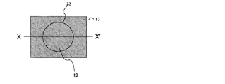
これら既存技術に対して、電圧パルスを印加することによって可逆的に電気抵抗が変化する可変抵抗素子を用いた抵抗性不揮発性メモリRRAM(Resistive Random Access Memory)(登録商標)が提案されている。この構成を図50に示す。 For these existing technologies, a resistive non-volatile memory RRAM (Resistive Random Access Memory) (registered trademark) using a variable resistive element whose electric resistance reversibly changes by applying a voltage pulse has been proposed. This configuration is shown in FIG.
図50に示されるように、従来構成の可変抵抗素子は、下部電極103と可変抵抗体102と上部電極101とが順に積層された構造となっており、上部電極101及び下部電極103間に電圧パルスを印加することにより、抵抗値を可逆的に変化させることができる性質を有する。この可逆的な抵抗変化動作(以下では「スイッチング動作」という)によって変化する抵抗値を読み出すことによって、新規な不揮発性半導体記憶装置が実現できる構成である。
As shown in FIG. 50, the variable resistance element of the conventional configuration has a structure in which a
この従来構成の可変抵抗素子としては、例えば、下記特許文献1において、半導体プロセスとの親和性が高く且つ単純な組成からなる2元系酸化物からなる抵抗変化型メモリが開示されている。具体的には、特許文献1には、「データ貯蔵物質層が、異なる電圧で異なる抵抗特性を有し、所定の電圧範囲で抵抗が急激に高くなる遷移金属酸化膜としてNiO、V2O5、ZnO、Nb2O5、TiO2、WO3またはCoOであることを特徴とする不揮発性メモリ装置」が開示されている。
As this conventional variable resistance element, for example,
また、下記非特許文献1には、上部電極および下部電極と、この2つの電極に挟まれた2元系遷移金属酸化物であるNiO、TiO2、ZrO2、またはHfO2とより構成される、不揮発性抵抗変化メモリ素子の例が報告されている。
これら特許文献1あるいは非特許文献1に開示されている2元系遷移金属酸化物からなる抵抗変化型メモリは、上述のように、半導体プロセスとの親和性が高く、且つ単純な構造・組成からなり、高集積不揮発メモリに適用し易いという利点がある。
As described above, the resistance change type memory made of the binary transition metal oxide disclosed in
上記の各従来技術によれば、素子の構造は、基板上に下部電極、可変抵抗体、上部電極の順に形成された積層構造の可変抵抗素子である。その素子の抵抗変化は、電圧パルス印加条件により、可変抵抗素子に流れ込む電流による熱上昇によって可変抵抗体中に局所的に抵抗率が低下した領域(以下、適宜「フィラメントパス」という)が形成されたり、フィラメントパスが分解されたりすることで、低抵抗や高抵抗となる現象に基づくものであるとされている。そして、スイッチング動作に先立ち、このフィラメントパスを形成すべく、通常のスイッチング動作に用いるよりも大きな電圧を印加する「フォーミングプロセス」と呼ばれる電気的処理が必要となる。 According to each of the conventional techniques described above, the element structure is a variable resistance element having a laminated structure in which a lower electrode, a variable resistor, and an upper electrode are formed in this order on a substrate. As for the resistance change of the element, a region in which the resistivity is locally reduced (hereinafter referred to as “filament path” as appropriate) is formed in the variable resistor due to the heat rise due to the current flowing into the variable resistance element depending on the voltage pulse application condition. It is said that this is based on the phenomenon that the resistance becomes low or high by disassembling the filament path. Prior to the switching operation, in order to form the filament path, an electrical process called a “forming process” for applying a voltage larger than that used in the normal switching operation is required.
このフォーミングプロセスは、例えば可変抵抗体がもともとほぼ絶縁体である金属酸化物である場合、通常のスイッチング動作に用いる電圧の数倍から10倍もの大きな電圧を一定時間以上印加しなくてはならない。そして、フォーミングプロセスでは、絶縁体における絶縁破壊に似た現象により電流パスを形成するため、可変抵抗体中において最も電気的に脆弱であったであろうフィラメントパスの形成場所を限定することはできない。このことが、可変抵抗素子の構造設計を困難にしている。 In this forming process, for example, when the variable resistor is a metal oxide that is essentially an insulator, a voltage several times to ten times as large as the voltage used for the normal switching operation must be applied for a certain time or more. In the forming process, the current path is formed by a phenomenon similar to dielectric breakdown in the insulator, and therefore, the formation location of the filament path that would have been most electrically fragile in the variable resistor cannot be limited. . This makes it difficult to design the structure of the variable resistance element.
また、フォーミングプロセス後の読み出し抵抗値にばらつきがあり、フォーミングプロセス後のフィラメントパスの状態制御はなされていない。フォーミングプロセス後の読み出し抵抗値が異なると、それぞれのスイッチング動作において、低抵抗状態の抵抗値、高抵抗状態の抵抗値、セット動作の電圧条件、リセット動作の電圧条件等が異なり、素子間の電気特性が均一性を欠いてしまう。 Further, there is a variation in the read resistance value after the forming process, and the filament path state control after the forming process is not performed. If the read resistance value after the forming process is different, the resistance value in the low resistance state, the resistance value in the high resistance state, the voltage condition in the set operation, the voltage condition in the reset operation, etc. are different in each switching operation. The characteristics are not uniform.
本発明は上記の問題点に鑑み、フォーミングプロセスによって形成されるフィラメントパスの形成領域を限定することで、スイッチング動作の再現性を高め、構造設計の容易化を可能にする可変抵抗素子を提供することを目的とする。 In view of the above-described problems, the present invention provides a variable resistance element that improves the reproducibility of switching operation and facilitates structural design by limiting the formation region of the filament path formed by the forming process. For the purpose.
上記目的を達成するための本発明に係る可変抵抗素子は、基板上に、第1電極、第2電極、及び前記両電極の間に形成される可変抵抗体を有し、前記両電極間に電圧パルスを印加することで前記両電極間の電気抵抗が可逆的に変化する可変抵抗素子であって、前記可変抵抗体が、前記第1電極から前記第2電極に向かう方向に延伸する少なくとも一つのシームを有することを特徴とする。 In order to achieve the above object, a variable resistance element according to the present invention has a first electrode, a second electrode, and a variable resistor formed between the two electrodes on a substrate, and between the two electrodes. A variable resistance element in which an electrical resistance between the electrodes changes reversibly by applying a voltage pulse, wherein the variable resistor extends in a direction from the first electrode toward the second electrode. It has two seams.
本発明に係る可変抵抗素子の上記特徴によれば、可変抵抗体膜内において、第1電極から第2電極に向かう方向に延伸するシームが形成されているため、両電極間に電圧を印加したとき、このシームをフィラメントパスとして利用することができる。すなわち、シームでは可変抵抗体内部(バルク部)に比べて構造欠陥が多いため、電界集中が起こりやすい。このため、フォーミングプロセスを行うべく電圧を印加したとき、電界集中が起こりやすいシーム内あるいはその近傍においてフィラメントパスが容易に形成しやすい状況となる。このため、予め製造時に特定箇所にシームを意図的に形成しておくことで、フォーミングプロセスによって形成されるフィラメントパスの形成領域を特定範囲内に収めることができ、スイッチング動作の再現性を高めることができる。 According to the above feature of the variable resistance element according to the present invention, since a seam extending in the direction from the first electrode to the second electrode is formed in the variable resistor film, a voltage is applied between both electrodes. Sometimes this seam can be used as a filament path. That is, since there are more structural defects in the seam than in the variable resistor (bulk portion), electric field concentration is likely to occur. For this reason, when a voltage is applied to perform the forming process, a filament path is easily formed in or near the seam where electric field concentration is likely to occur. For this reason, by intentionally forming a seam at a specific location in advance during manufacturing, the filament path formation region formed by the forming process can be kept within a specific range, and the reproducibility of the switching operation is improved. Can do.
また、前記のとおり、シーム内あるいはその近傍において電界集中が起こりやすい構成であるため、従来構成よりもフォーミングプロセス実行に要する電圧を低電圧化することができる。 In addition, as described above, since the electric field concentration is likely to occur in or near the seam, the voltage required for executing the forming process can be reduced as compared with the conventional configuration.
なお、上記特徴において、シームの形状は線状、環状または離散した点状であっても良い。また、必ずしも第1電極及び第2電極の一方あるいは双方に接触するようにシームが形成される必要はなく、両電極の双方に接触することなく可変抵抗体膜内にシームが形成されていても良い。この場合であっても、フォーミングプロセスを実行することで、シーム形成領域においては、シーム内あるいはその近傍にフィラメントパスが形成されるため、シームが全く形成されていない従来構成と比較してフィラメントパスの形成領域が特定でき、再現性良くスイッチング動作を行うことができる。 In the above feature, the shape of the seam may be linear, annular, or discrete point. Further, it is not always necessary to form the seam so as to contact one or both of the first electrode and the second electrode, and even if the seam is formed in the variable resistor film without contacting both the electrodes. good. Even in this case, by performing the forming process, a filament path is formed in or near the seam in the seam formation region. Therefore, the filament path is compared with the conventional configuration in which no seam is formed. The forming region can be specified, and the switching operation can be performed with good reproducibility.
また、上記可変抵抗体膜としては、Ti,V,Mn,Fe,Co,Ni,Zn,Zr,Nb,Hf,Ta,W等の金属の酸化物または酸窒化物を利用することができる。 Further, as the variable resistor film, it is possible to use oxides or oxynitrides of metals such as Ti, V, Mn, Fe, Co, Ni, Zn, Zr, Nb, Hf, Ta, and W.
このとき、前記可変抵抗体膜が局部的に厚膜化している厚膜領域内にシームが形成される構成としても構わない。ここでいう「厚膜領域」とは、可変抵抗体膜の表裏両面(一方の面は少なくとも一部が第1電極と接触し、他方の面は少なくとも一部が第2電極と接触する)の一方の面上において、当該面上の点か他方の面上の点までの最短距離が、堆積膜厚(表裏両面が平行して延在している部分の膜厚)より長くなっている領域を指す。例えば、段差部に形成された可変抵抗体膜においては、段差のコーナ領域に相当し、開口部内を充填されるように形成された可変抵抗体膜においては、当該開口部内の軸心領域に相当する。 At this time, a seam may be formed in a thick film region where the variable resistor film is locally thickened. The “thick film region” as used herein refers to both the front and back surfaces of the variable resistor film (one surface is at least partially in contact with the first electrode and the other surface is at least partially in contact with the second electrode). On one surface, the shortest distance from the point on the surface to the point on the other surface is longer than the deposited film thickness (the film thickness of the portion where both the front and back surfaces extend in parallel) Point to. For example, the variable resistor film formed in the step portion corresponds to the corner region of the step, and the variable resistor film formed so as to fill the opening portion corresponds to the axial center region in the opening portion. To do.
また、本発明に係る可変抵抗素子は、上記特徴に加えて、少なくとも一つの前記シームが、前記第1電極と前記第2電極との間に電圧が印加されることでフィラメントパスの一部を形成することを別の特徴とする。 In addition to the above characteristics, the variable resistance element according to the present invention may be configured such that at least one of the seams applies a voltage between the first electrode and the second electrode, thereby forming a part of the filament path. Another feature is forming.
また、本発明に係る可変抵抗素子は、上記特徴に加えて、前記可変抵抗体が、前記基板面に平行に構成される第1構造部と、下端が前記第1構造部の端部と結合し前記基板面に垂直な方向に構成される第2構造部とを備え、前記第1構造部と前記第2構造部とが結合するコーナ領域に前記シームを有することを別の特徴とする。 In addition to the above features, the variable resistance element according to the present invention is configured such that the variable resistor is coupled to a first structure portion configured parallel to the substrate surface, and a lower end is coupled to an end portion of the first structure portion. And a second structure portion configured in a direction perpendicular to the substrate surface, and the seam is provided in a corner region where the first structure portion and the second structure portion are coupled to each other.
このとき、本発明に係る可変抵抗素子は、上記特徴に加えて、前記第1電極の一部上層に絶縁膜を有し、前記可変抵抗体は、前記第1構造部において、下面が前記第1電極の上面と接触し、上面が前記第2電極の下面と接触し、前記第2構造部において、第1面が前記絶縁膜の側面と接触し、前記第1面と当該可変抵抗体の膜厚を隔てて対向する第2面が前記第2電極の側面と接触するように形成されているものとしても構わない。 In this case, in addition to the above characteristics, the variable resistance element according to the present invention includes an insulating film on a part of the first electrode. The upper surface is in contact with the upper surface of one electrode, the upper surface is in contact with the lower surface of the second electrode, and in the second structure portion, the first surface is in contact with the side surface of the insulating film, and the first surface and the variable resistor are The second surfaces facing each other with a film thickness may be formed so as to be in contact with the side surface of the second electrode.
また、本発明に係る可変抵抗素子は、上記特徴に加えて、前記第1電極と同一層において前記第1電極よりも膜厚が厚い絶縁膜を有し、前記可変抵抗体は、前記第1構造部において、下面が前記第1電極の上面と接触し、上面が前記第2電極の下面と接触し、前記第2構造部において、第1面が前記絶縁膜の側面と接触し、前記第1面と当該可変抵抗体の膜厚を隔てて対向する第2面が前記第2電極の側面と接触するように形成されているものとしても構わない。 In addition to the above features, the variable resistance element according to the present invention includes an insulating film that is thicker than the first electrode in the same layer as the first electrode, and the variable resistor includes the first resistor. In the structure portion, the lower surface is in contact with the upper surface of the first electrode, the upper surface is in contact with the lower surface of the second electrode, and in the second structure portion, the first surface is in contact with the side surface of the insulating film, A second surface opposing one surface with a film thickness of the variable resistor may be formed so as to be in contact with the side surface of the second electrode.
このとき、前記可変抵抗体が、前記基板面に平行に構成され前記第1構造部より高さ位置が高く、端部において前記第2構造部の上端と結合する第3構造部を備え、前記第3構造部において、下面が前記絶縁膜の上面と接触し、上面が前記第2電極の下面と接触するように形成されているものとしても構わない。 At this time, the variable resistor includes a third structure portion configured parallel to the substrate surface and having a height position higher than that of the first structure portion and coupled to an upper end of the second structure portion at an end portion, In the third structure portion, the lower surface may be formed so as to be in contact with the upper surface of the insulating film, and the upper surface may be formed in contact with the lower surface of the second electrode.
また、本発明に係る可変抵抗素子は、上記特徴に加えて、前記第1電極は、形成膜厚が異なる領域を有することで段差を有する構成であり、前記可変抵抗体は、前記第1構造部において、下面が前記第1電極の上面と接触し、上面が前記第2電極の下面と接触し、前記第2構造部において、第1面が前記第1電極の側面と接触し、前記第1面と当該可変抵抗体の膜厚を隔てて対向する第2面が前記第2電極の側面と接触するように形成されているものとしても構わない。 In addition to the above characteristics, the variable resistance element according to the present invention has a configuration in which the first electrode has a step by having regions with different formation film thicknesses, and the variable resistor has the first structure. The lower surface is in contact with the upper surface of the first electrode, the upper surface is in contact with the lower surface of the second electrode, and in the second structure portion, the first surface is in contact with the side surface of the first electrode, A second surface opposing one surface with a film thickness of the variable resistor may be formed so as to be in contact with the side surface of the second electrode.
また、本発明に係る可変抵抗素子は、上記特徴に加えて、形成膜厚が異なる領域を有することで段差を有する絶縁膜を備え、前記第1電極が、前記絶縁膜上に形成されることで最上位面に高さ位置の差異を有した状態で形成されており、前記可変抵抗体は、前記第1構造部において、下面が前記第1電極の上面と接触し、上面が前記第2電極の下面と接触し、前記第2構造部において、第1面が前記第1電極の側面と接触し、前記第1面と当該可変抵抗体の膜厚を隔てて対向する第2面が前記第2電極の側面と接触するように形成されているものとしても構わない。 In addition to the above characteristics, the variable resistance element according to the present invention includes an insulating film having a step by having regions with different formed film thicknesses, and the first electrode is formed on the insulating film. The variable resistor has a lower surface in contact with the upper surface of the first electrode in the first structure portion, and the upper surface is in the second structure. The second surface is in contact with the lower surface of the electrode, and in the second structure portion, the first surface is in contact with the side surface of the first electrode, and the second surface facing the first surface with a film thickness of the variable resistor is It may be formed so as to be in contact with the side surface of the second electrode.
また、本発明に係る可変抵抗素子は、上記特徴に加えて、絶縁膜を備え、前記第1電極が前記絶縁膜の一部上層に形成されており、前記可変抵抗体は、前記第1構造部において、下面が前記絶縁膜の上面と接触し、上面が前記第2電極の下面と接触し、前記第2構造部において、第1面が前記第1電極の側面と接触し、前記第1面と当該可変抵抗体の膜厚を隔てて対向する第2面が前記第2電極の側面と接触するように形成されているものとしても構わない。 In addition to the above features, the variable resistance element according to the present invention includes an insulating film, the first electrode is formed on a part of the insulating film, and the variable resistor includes the first structure. In the portion, the lower surface is in contact with the upper surface of the insulating film, the upper surface is in contact with the lower surface of the second electrode, and in the second structure portion, the first surface is in contact with the side surface of the first electrode, and the first The second surface that faces the surface of the variable resistor with the film thickness of the variable resistor may be formed so as to be in contact with the side surface of the second electrode.
また、本発明に係る可変抵抗素子は、上記特徴に加えて、前記第1電極と同一層において前記第1電極よりも膜厚が薄い絶縁膜を有し、前記可変抵抗体は、前記第1構造部において、下面が前記絶縁膜の上面と接触し、上面が前記第2電極の下面と接触し、前記第2構造部において、第1面が前記第1電極の側面と接触し、前記第1面と当該可変抵抗体の膜厚を隔てて対向する第2面が前記第2電極の側面と接触するように形成されているものとしても構わない。 The variable resistance element according to the present invention includes, in addition to the above characteristics, an insulating film having a thickness smaller than that of the first electrode in the same layer as the first electrode. In the structure portion, the lower surface is in contact with the upper surface of the insulating film, the upper surface is in contact with the lower surface of the second electrode, and in the second structure portion, the first surface is in contact with the side surface of the first electrode, A second surface opposing one surface with a film thickness of the variable resistor may be formed so as to be in contact with the side surface of the second electrode.
このとき、前記可変抵抗体が、前記基板面に平行に構成され前記第1構造部より高さ位置が高く、端部において前記第2構造部の上端と結合する第3構造部を備え、前記第3構造部において、下面が前記第1電極の上面と接触し、上面が前記第2電極の下面と接触するように形成されているものとしても構わない。 At this time, the variable resistor includes a third structure portion configured parallel to the substrate surface and having a height position higher than that of the first structure portion and coupled to an upper end of the second structure portion at an end portion, In the third structure portion, the lower surface may be formed so as to be in contact with the upper surface of the first electrode, and the upper surface may be in contact with the lower surface of the second electrode.
さらに、本発明に係る可変抵抗素子は、上記特徴に加えて、前記第2構造部が、前記基板面に平行な断面が環状に形成されるとともに、当該第2構造部の内側において下端と前記第1構造部の端部とが結合する構成としても構わない。 Furthermore, in addition to the above characteristics, the variable resistance element according to the present invention is configured such that the second structure portion has an annular cross section parallel to the substrate surface, and the lower end and the inner side of the second structure portion. A configuration in which the end portion of the first structure portion is coupled may be possible.
このとき、本発明に係る可変抵抗素子は、前記第1電極の一部上層に絶縁膜を備え、前記可変抵抗体は、前記第1構造部において、下面が前記第1電極の上面と接触し、上面が前記第2電極の下面と接触し、前記第2構造部において、外側面が前記絶縁膜の側面と接触し、前記外側面と当該可変抵抗体の膜厚を隔てて対向する内側面が前記第2電極の側面と接触するように形成されているものとしても構わない。 At this time, the variable resistance element according to the present invention includes an insulating film on a part of the first electrode, and the variable resistor has a lower surface in contact with the upper surface of the first electrode in the first structure portion. The upper surface is in contact with the lower surface of the second electrode, and in the second structure portion, the outer surface is in contact with the side surface of the insulating film, and the inner surface is opposed to the outer surface with a film thickness of the variable resistor. May be formed so as to be in contact with the side surface of the second electrode.
また、本発明に係る可変抵抗素子は、上記特徴に加えて、前記第1電極と同一層において前記第1電極よりも膜厚が厚い絶縁膜を有し、前記可変抵抗体は、前記第1構造部において、下面が前記第1電極の上面と接触し、上面が前記第2電極の下面と接触し、前記第2構造部において、外側面が前記絶縁膜の側面と接触し、前記外側面と当該可変抵抗体の膜厚を隔てて対向する内側面が前記第2電極の側面と接触するように形成されているものとしても構わない。 In addition to the above features, the variable resistance element according to the present invention includes an insulating film that is thicker than the first electrode in the same layer as the first electrode, and the variable resistor includes the first resistor. In the structure portion, the lower surface is in contact with the upper surface of the first electrode, the upper surface is in contact with the lower surface of the second electrode, and in the second structure portion, the outer surface is in contact with the side surface of the insulating film, And the inner surface facing the variable resistor with a film thickness therebetween may be formed so as to be in contact with the side surface of the second electrode.
このとき、本発明に係る可変抵抗素子は、前記可変抵抗体が、前記基板面に平行に構成され前記第1構造部より高さ位置が高く、前記第2構造部の外側において端部が前記第2構造部の上端と結合する第3構造部を備え、前記第3構造部において、下面が前記絶縁膜の上面と接触し、上面が前記第2電極の下面と接触するように形成されているものとしても構わない。 At this time, in the variable resistance element according to the present invention, the variable resistor is configured to be parallel to the substrate surface and has a height position higher than that of the first structure portion, and an end portion of the variable resistor element is outside the second structure portion. A third structure unit coupled to the upper end of the second structure unit, wherein the lower surface of the third structure unit is in contact with the upper surface of the insulating film, and the upper surface is in contact with the lower surface of the second electrode; It doesn't matter if you have
また、本発明に係る可変抵抗素子は、上記特徴に加えて、前記第1電極は、形成膜厚が異なる領域を有することで段差を有する構成であり、前記可変抵抗体は、前記第1構造部において、下面が前記第1電極の上面と接触し、上面が前記第2電極の下面と接触し、前記第2構造部において、外側面が前記第1電極の側面と接触し、前記外側面と当該可変抵抗体の膜厚を隔てて対向する内側面が前記第2電極の側面と接触するように形成されているものとしても構わない。 In addition to the above characteristics, the variable resistance element according to the present invention has a configuration in which the first electrode has a step by having regions with different formation film thicknesses, and the variable resistor has the first structure. The lower surface is in contact with the upper surface of the first electrode, the upper surface is in contact with the lower surface of the second electrode, and in the second structure portion, the outer surface is in contact with the side surface of the first electrode, and the outer surface And the inner surface facing the variable resistor with a film thickness therebetween may be formed so as to be in contact with the side surface of the second electrode.
また、本発明に係る可変抵抗素子は、上記特徴に加えて、形成膜厚が異なる領域を有することで段差を有する絶縁膜を備え、前記第1電極が、前記絶縁膜上に形成されることで最上位面に高さ位置の差異を有した状態で形成されており、前記可変抵抗体は、前記第1構造部において、下面が前記第1電極の上面と接触し、上面が前記第2電極の下面と接触し、前記第2構造部において、外側面が前記第1電極の側面と接触し、前記外側面と当該可変抵抗体の膜厚を隔てて対向する内側面が前記第2電極の側面と接触するように形成されているものとしても構わない。 In addition to the above characteristics, the variable resistance element according to the present invention includes an insulating film having a step by having regions with different formed film thicknesses, and the first electrode is formed on the insulating film. The variable resistor has a lower surface in contact with the upper surface of the first electrode in the first structure portion, and the upper surface is in the second structure. In contact with the lower surface of the electrode, in the second structure portion, the outer surface is in contact with the side surface of the first electrode, and the inner surface facing the outer surface with a film thickness of the variable resistor is the second electrode. It may be formed so as to be in contact with the side surface of the plate.
また、本発明に係る可変抵抗素子は、上記特徴に加えて、絶縁膜を備え、前記第1電極が前記絶縁膜の一部上層に形成されており、前記可変抵抗体は、 前記第1構造部において、下面が前記絶縁膜の上面と接触し、上面が前記第2電極の下面と接触し、前記第2構造部において、外側面が前記第1電極の側面と接触し、前記外側面と当該可変抵抗体の膜厚を隔てて対向する内側面が前記第2電極の側面と接触するように形成されているものとしても構わない。 In addition to the above features, the variable resistance element according to the present invention further includes an insulating film, the first electrode is formed on a part of the insulating film, and the variable resistor includes the first structure. The lower surface is in contact with the upper surface of the insulating film, the upper surface is in contact with the lower surface of the second electrode, and in the second structure portion, the outer surface is in contact with the side surface of the first electrode, The inner surface which opposes across the film thickness of the variable resistor may be formed so as to be in contact with the side surface of the second electrode.
また、本発明に係る可変抵抗素子は、上記特徴に加えて、前記第1電極と同一層において前記第1電極よりも膜厚が薄い絶縁膜を有し、前記可変抵抗体は、前記第1構造部において、下面が前記絶縁膜の上面と接触し、上面が前記第2電極の下面と接触し、前記第2構造部において、外側面が前記第1電極の側面と接触し、前記外側面と当該可変抵抗体の膜厚を隔てて対向する内側面が前記第2電極の側面と接触するように形成されているものとしても構わない。 The variable resistance element according to the present invention includes, in addition to the above characteristics, an insulating film having a thickness smaller than that of the first electrode in the same layer as the first electrode. In the structure portion, the lower surface is in contact with the upper surface of the insulating film, the upper surface is in contact with the lower surface of the second electrode, and in the second structure portion, the outer surface is in contact with the side surface of the first electrode, and the outer surface. And the inner surface facing the variable resistor with a film thickness therebetween may be formed so as to be in contact with the side surface of the second electrode.
このとき、本発明に係る可変抵抗素子は、前記可変抵抗体が、前記基板面に平行に構成され前記第1構造部より高さ位置が高く、前記第2構造部の外側において端部が前記第2構造部の上端と結合する第3構造部を備え、前記第3構造部において、下面が前記第1電極の上面と接触し、上面が前記第2電極の下面と接触するように形成されているものとしても構わない。 At this time, in the variable resistance element according to the present invention, the variable resistor is configured to be parallel to the substrate surface and has a height position higher than that of the first structure portion, and an end portion of the variable resistor element is outside the second structure portion. A third structure unit coupled to an upper end of the second structure unit, wherein the lower surface of the third structure unit is in contact with the upper surface of the first electrode and the upper surface is in contact with the lower surface of the second electrode; It does not matter as long as it is.
また、本発明に係る可変抵抗素子は、上記特徴に加えて、前記可変抵抗体が、少なくとも外側面が同一の材料膜で囲まれた埋め込み領域内に埋め込まれて形成され、前記埋め込み領域内において高さ方向に延伸する前記シームを有する構成であって、前記材料膜が、前記第1電極または絶縁膜で構成されているものとしても構わない。 In addition to the above features, the variable resistance element according to the present invention is formed by embedding the variable resistor in a buried region surrounded by the same material film at least on the outer surface. The seam extending in the height direction may be included, and the material film may be configured by the first electrode or the insulating film.
このとき、さらに本発明に係る可変抵抗素子は、前記第1電極の一部上層に前記絶縁膜を備え、前記可変抵抗体は、前記埋め込み領域内において、下面が前記絶縁膜の上面と接触し、前記外側面が前記絶縁膜の側面と接触するように形成されているものとしても構わない。 At this time, the variable resistance element according to the present invention further includes the insulating film on a part of the first electrode, and the variable resistor has a lower surface in contact with the upper surface of the insulating film in the buried region. The outer surface may be formed so as to be in contact with the side surface of the insulating film.
また、本発明に係る可変抵抗素子は、上記特徴に加えて、前記第1電極は、形成膜厚が異なる領域を有することで段差を有する構成であり、前記可変抵抗体は、前記埋め込み領域内において、下面が前記第1電極の上面と接触し、前記外側面が前記第1電極の側面と接触するように形成されているものとしても構わない。 In addition to the above characteristics, the variable resistance element according to the present invention has a configuration in which the first electrode has a step by having regions having different formation thicknesses, and the variable resistor is in the embedded region. , The lower surface may be in contact with the upper surface of the first electrode, and the outer surface may be formed in contact with the side surface of the first electrode.
このとき、本発明に係る可変抵抗素子は、前記可変抵抗体が、前記埋め込み領域の外側に係る埋め込み外領域内において、前記埋め込み領域内に形成されている当該可変抵抗体と連結し、且つ前記埋め込み領域内の最下面よりも最下面の高さ位置が高くなるように形成されており、前記埋め込み外領域内において、下面が前記絶縁膜の上面と接触し、上面が前記第2電極の下面と接触する構成としても構わない。 At this time, in the variable resistance element according to the present invention, the variable resistor is connected to the variable resistor formed in the buried region in the buried outer region outside the buried region, and The lowermost surface is formed so that the height of the lowermost surface is higher than the lowermost surface in the buried region, the lower surface is in contact with the upper surface of the insulating film in the outer region, and the upper surface is the lower surface of the second electrode. It does not matter even if it contacts with.
また、本発明に係る可変抵抗素子は、上記特徴に加えて、前記第1電極は、形成膜厚が異なる領域を有することで段差を有する絶縁膜を備え、前記第1電極が、前記絶縁膜上に形成されることで最上位面に高さ位置の差異を有した状態で形成されており、前記可変抵抗体は、前記埋め込み領域内において、下面が前記第1電極の上面と接触し、前記外側面が前記第1電極の側面と接触するように形成されている厚が異なる領域を有することで段差を有する構成であり、前記可変抵抗体は、前記埋め込み領域内において、下面が前記第1電極の上面と接触し、前記外側面が前記第1電極の側面と接触するように形成されているものとしても構わない。 In addition to the above characteristics, the variable resistance element according to the present invention includes an insulating film having a step due to a region having a different formation film thickness, and the first electrode includes the insulating film. The variable resistor is formed in a state having a height position difference on the uppermost surface, and the lower surface of the variable resistor is in contact with the upper surface of the first electrode in the embedded region, The variable resistor is configured to have a step by having a region having a different thickness formed so that the outer surface is in contact with the side surface of the first electrode, and the lower surface of the variable resistor is in the embedded region. The outer surface may be in contact with the upper surface of one electrode, and the outer surface may be in contact with the side surface of the first electrode.
なお、ここで前記埋め込み領域内の可変抵抗体の形状は、柱状に限られるものではなく、例えば底面に行くほど基板面に平行な断面積が縮小する錐体状であっても構わないし、その他の形状であっても良い。 Here, the shape of the variable resistor in the embedded region is not limited to the columnar shape, and may be a cone shape whose cross-sectional area parallel to the substrate surface decreases toward the bottom surface, for example. The shape may also be
また、本発明に係る可変抵抗素子は、前記可変抵抗体が、前記埋め込み領域の外側に係る埋め込み外領域内において、前記埋め込み領域内に形成されている当該可変抵抗体と連結し、且つ前記埋め込み領域内の最下面よりも最下面の高さ位置が高くなるように形成されており、前記埋め込み外領域内において、下面が前記第1電極の上面と接触し、上面が前記第2電極の下面と接触するものとしても構わない。 In the variable resistance element according to the present invention, the variable resistor is connected to the variable resistor formed in the embedded region in the embedded outer region outside the embedded region, and the embedded The lowermost surface is formed so that the height of the lowermost surface is higher than the lowermost surface in the region, and the lower surface is in contact with the upper surface of the first electrode and the upper surface is the lower surface of the second electrode. It may be in contact with
また、本発明に係る可変抵抗素子の製造方法は、前記基板上にシーム形成用段差を形成する段差形成工程と、その後に、前記可変抵抗体を形成する可変抵抗体形成工程と、その後に、前記第2電極を形成する第2電極形成工程と、を有し、前記段差形成工程が、前記第1電極を形成する工程を含み、前記第1電極を形成することで、前記基板面に平行な第1上面、前記基板面に平行に構成され前記第1上面より高さ位置の低い第2上面、並びに上端が前記第1上面の端部と結合し下端が前記第2上面の端部と結合することで前記第1上面と前記第2上面とを前記基板面に垂直な方向に連絡する中間面を有するとともに少なくとも前記第2上面または前記中間面のいずれか一方の面が前記第1電極で構成された前記シーム形成用段差を形成する工程であり、前記可変抵抗体形成工程が、全面に可変抵抗体膜をスパッタリング法によって成膜するか、もしくは、全面に所定の材料膜をスパッタリング法によって成膜した後に酸化処理を行って可変抵抗体膜を形成することで、前記可変抵抗体膜が前記第2上面に接触する前記第1構造部、及び前記可変抵抗体膜が前記中間面に接触する前記第2構造部を含む前記可変抵抗体を形成するとともに、前記第1構造部と前記第2構造部とが結合する前記コーナ領域に係る前記可変抵抗体内に前記シームを形成する工程であり、前記第2電極形成工程が、前記シームが形成された前記可変抵抗体膜の上面に前記第2電極を形成する工程であることを特徴とする。 The variable resistance element manufacturing method according to the present invention includes a step forming step for forming a seam forming step on the substrate, a variable resistor forming step for forming the variable resistor, and A second electrode forming step of forming the second electrode, wherein the step forming step includes a step of forming the first electrode, and forming the first electrode makes it parallel to the substrate surface. A first upper surface, a second upper surface configured parallel to the substrate surface and lower in height than the first upper surface, an upper end coupled to an end portion of the first upper surface, and a lower end coupled to an end portion of the second upper surface. An intermediate surface that connects the first upper surface and the second upper surface in a direction perpendicular to the substrate surface by coupling and at least one of the second upper surface and the intermediate surface is the first electrode. Forming the seam forming step composed of In the variable resistor forming step, the variable resistor film is formed on the entire surface by a sputtering method, or a predetermined material film is formed on the entire surface by a sputtering method, and then an oxidation treatment is performed to change the variable resistor film. By forming a body film, the variable resistor film includes the first structure part in which the variable resistor film contacts the second upper surface, and the second structure part in which the variable resistor film contacts the intermediate surface. Forming a seam, and forming the seam in the variable resistor in the corner region where the first structure part and the second structure part are coupled, and the second electrode forming process comprises the seam This is a step of forming the second electrode on the upper surface of the variable resistor film on which is formed.
本発明に係る可変抵抗素子の製造方法の上記特徴によれば、段差形成工程において第2上面または中間面が第1電極で構成されるシーム形成用段差が形成された後、可変抵抗体膜を全面に成膜する。そして、このときシームが形成されないような措置を施すことなく可変抵抗体膜を成膜することが肝要である。これにより、可変抵抗体膜が第1電極に接触しながらも、第2上面から成長する可変抵抗体膜と中間面から成長する可変抵抗体膜とが結合するコーナ領域において、第2上面と中間面が結合する領域すなわち第1電極の形成側領域から第2上面の上方に向かう方向に延伸するシームを意図的に形成することができる。そして、このシームが形成された可変抵抗体膜の上面に第2電極を形成することで、第1電極と第2電極に狭持され、内部にシームを有する可変抵抗体を備える可変抵抗素子を製造することができる。 According to the above feature of the variable resistance element manufacturing method according to the present invention, after the step for forming the seam is formed in which the second upper surface or the intermediate surface is formed by the first electrode in the step forming step, the variable resistor film is formed. A film is formed on the entire surface. At this time, it is important to form the variable resistor film without taking measures to prevent the seam from being formed. Accordingly, in the corner region where the variable resistor film growing from the second upper surface and the variable resistor film growing from the intermediate surface are coupled to each other while the variable resistor film is in contact with the first electrode, It is possible to intentionally form a seam extending in a direction from the region where the surfaces are combined, that is, the region where the first electrode is formed to the second upper surface. Then, by forming the second electrode on the upper surface of the variable resistor film on which the seam is formed, a variable resistance element having a variable resistor sandwiched between the first electrode and the second electrode and having a seam inside is provided. Can be manufactured.
なお、上記可変抵抗体膜としては、Ti,V,Mn,Fe,Co,Ni,Zn,Zr,Nb,Hf,Ta,W等の金属の酸化物または酸窒化物を利用することができる。このとき、可変抵抗体形成工程では、金属酸化物または酸窒化物で構成される前記可変抵抗体膜をそのまま成膜する構成としても構わないし、金属膜または金属窒化物膜を成膜した後に酸化処理を施して上記可変抵抗体膜を形成するものとしても構わない。 As the variable resistor film, a metal oxide or oxynitride such as Ti, V, Mn, Fe, Co, Ni, Zn, Zr, Nb, Hf, Ta, and W can be used. At this time, in the variable resistor forming step, the variable resistor film made of metal oxide or oxynitride may be formed as it is, or the metal film or metal nitride film may be oxidized after being formed. Processing may be performed to form the variable resistor film.
また、本発明に係る可変抵抗素子の製造方法は、上記特徴に加えて、前記段差形成工程において、前記基板上に前記第1電極を形成し、その後に、前記第1電極の上面に絶縁膜を成膜した後、前記絶縁膜に対して前記第1電極の一部上面が露出するまでエッチングを施すことで、前記絶縁膜で構成された前記第1上面及び前記中間面、並びに前記第1電極で構成された前記第2上面を有する前記シーム形成用段差を形成するものとしても構わない。 In addition to the above features, the variable resistance element manufacturing method according to the present invention includes forming the first electrode on the substrate in the step forming step, and then forming an insulating film on the upper surface of the first electrode. After the film is formed, the insulating film is etched until a partial upper surface of the first electrode is exposed, whereby the first upper surface and the intermediate surface formed of the insulating film, and the first The seam forming step having the second upper surface constituted by electrodes may be formed.
また、本発明に係る可変抵抗素子の製造方法は、上記特徴に加えて、前記段差形成工程において、前記基板上の一部領域に前記第1電極を、前記基板上の前記第1電極の形成外領域に前記第1電極より膜厚の厚い絶縁膜を形成することで、前記絶縁膜で構成された前記第1上面及び前記中間面、並びに前記第1電極で構成された前記第2上面を有する前記シーム形成用段差を形成するものとしても構わない。 In addition to the above features, the variable resistance element manufacturing method according to the present invention includes forming the first electrode in a partial region on the substrate and forming the first electrode on the substrate in the step forming step. By forming an insulating film thicker than the first electrode in the outer region, the first upper surface and the intermediate surface made of the insulating film, and the second upper surface made of the first electrode are formed. The seam forming step may be formed.
また、本発明に係る可変抵抗素子の製造方法は、上記特徴に加えて、前記段差形成工程において、前記基板上に前記第1電極を構成する電極膜を成膜し、その後に、一部領域に係る前記電極膜に対してエッチングを施すことで、前記第1上面、前記中間面、及び前記第2上面が全て前記第1電極で構成された前記シーム形成用段差を形成するものとしても構わない。 In addition to the above characteristics, the variable resistance element manufacturing method according to the present invention forms an electrode film constituting the first electrode on the substrate in the step forming step, and then a partial region. Etching may be performed on the electrode film according to the above to form the seam forming step in which the first upper surface, the intermediate surface, and the second upper surface are all configured by the first electrode. Absent.
また、本発明に係る可変抵抗素子の製造方法は、上記特徴に加えて、前記段差形成工程において、前記基板上に絶縁膜を成膜した後、一部領域にエッチングを施すことで前記絶縁膜に段差を形成し、その後に、前記段差が形成された前記絶縁膜の上面全面に前記第1電極を構成する電極膜を成膜することで、前記第1上面、前記中間面、及び前記第2上面が全て前記第1電極で構成された前記シーム形成用段差を形成するものとしても構わない。 In addition to the above characteristics, the method of manufacturing a variable resistance element according to the present invention includes, in the step forming step, forming an insulating film on the substrate and then etching a part of the insulating film to form the insulating film. And forming an electrode film constituting the first electrode on the entire upper surface of the insulating film on which the step is formed, thereby forming the first upper surface, the intermediate surface, and the first surface. It is possible to form the seam-forming step whose entire upper surface is composed of the first electrode.
また、本発明に係る可変抵抗素子の製造方法は、上記特徴に加えて、前記段差形成工程において、前記基板上に絶縁膜を形成し、その後に、前記絶縁膜の上面に前記第1電極を構成する電極膜を成膜した後、前記電極膜に対して前記絶縁膜の一部上面が露出するまでエッチングを施して前記第1電極を形成することで、前記第1電極で構成された前記第1上面及び前記中間面、並びに前記絶縁膜で構成された前記第2上面を有する前記シーム形成用段差を形成するものとしても構わない。 In addition to the above features, the variable resistance element manufacturing method according to the present invention further includes forming an insulating film on the substrate in the step forming step, and then forming the first electrode on the upper surface of the insulating film. After forming the electrode film to be formed, the first electrode is formed by performing etching until the upper surface of the insulating film is partially exposed to the electrode film, thereby forming the first electrode. The seam forming step having the first upper surface, the intermediate surface, and the second upper surface made of the insulating film may be formed.
また、本発明に係る可変抵抗素子の製造方法は、上記特徴に加えて、前記段差形成工程において、前記基板上の一部領域に前記第1電極を形成するとともに、前記基板上の前記第1電極形成外領域に前記第1電極より膜厚の薄い絶縁膜を形成することで、前記第1電極で構成された前記第1上面及び前記中間面、並びに前記絶縁膜で構成された前記第2上面を有する前記シーム形成用段差を形成するものとしても構わない。 In addition to the above characteristics, the variable resistance element manufacturing method according to the present invention forms the first electrode in a partial region on the substrate in the step forming step, and the first electrode on the substrate. By forming an insulating film having a thickness smaller than that of the first electrode in a region outside the electrode formation, the first upper surface and the intermediate surface configured by the first electrode, and the second configured by the insulating film. The seam forming step having an upper surface may be formed.
また、本発明に係る可変抵抗素子の製造方法は、前記基板上にシーム形成用開口部を形成する開口部形成工程と、その後に、前記可変抵抗体を形成する可変抵抗体形成工程と、その後に、前記第2電極を形成する第2電極形成工程と、を有し、前記開口部形成工程が、前記第1電極を形成する工程を含み、前記第1電極を形成することで、前記基板面に平行な断面が環状に形成された露出内側面、前記露出内側面の外側において前記露出内側面の上端と端部が結合する第1上面、並びに前記露出内側面の内側において前記露出内側面の下端と端部が結合する露出底面を有するとともに、少なくとも前記露出内側面または前記露出底面のいずれか一方の面が前記第1電極で構成された前記シーム形成用開口部を形成する工程であり、前記可変抵抗体形成工程が、全面に可変抵抗体膜をスパッタリング法によって成膜するか、もしくは、全面に所定の材料膜をスパッタリング法によって成膜した後に酸化処理を行って前記シーム形成用開口部内を完全には充填しない膜厚条件下で可変抵抗体膜を形成することで、前記可変抵抗体膜が前記露出底面に接触する前記第1構造部、及び前記可変抵抗体膜が前記露出内側面に接触する前記第2構造部を含む前記可変抵抗体を形成するとともに、前記第1構造部と前記第2構造部とが結合する前記コーナ領域に係る前記可変抵抗体内に前記シームを形成する工程であり、前記第2電極形成工程が、前記シームが形成された前記可変抵抗体膜の上面に前記第2電極を形成する工程であることを特徴とする。 The variable resistance element manufacturing method according to the present invention includes an opening forming step of forming a seam forming opening on the substrate, a variable resistor forming step of forming the variable resistor, and a subsequent step. A second electrode forming step of forming the second electrode, wherein the opening forming step includes a step of forming the first electrode, and the first electrode is formed to form the substrate. An exposed inner surface having an annular cross section parallel to the surface, a first upper surface where an upper end and an end of the exposed inner surface are joined outside the exposed inner surface, and the exposed inner surface inside the exposed inner surface Forming a seam-forming opening in which at least one of the exposed inner surface and the exposed bottom surface is configured by the first electrode. , The variable resistance In the body forming step, a variable resistor film is formed on the entire surface by a sputtering method, or a predetermined material film is formed on the entire surface by a sputtering method, and then an oxidation treatment is performed to completely complete the inside of the seam forming opening. Forming the variable resistor film under a film thickness condition that does not fill the first structure portion where the variable resistor film contacts the exposed bottom surface, and the variable resistor film contacts the exposed inner surface Forming the variable resistor including the second structure part, and forming the seam in the variable resistor in the corner region where the first structure part and the second structure part are coupled; The second electrode forming step is a step of forming the second electrode on an upper surface of the variable resistor film on which the seam is formed.
本発明に係る可変抵抗素子の製造方法の上記特徴によれば、開口部形成工程において露出内側面または露出底面が第1電極で構成されるシーム形成用開口部が形成された後、シーム形成用開口部内を完全には充填しない膜厚条件下で可変抵抗体膜を全面に成膜する。このときシームが形成されないような措置を施すことなく可変抵抗体膜を成膜することが肝要である。これにより、可変抵抗体膜が第1電極に接触しながらも、露出底面から成長する可変抵抗体膜と露出内側面から成長する可変抵抗体膜とが結合するコーナ領域において、露出底面と露出内側面が結合する領域すなわち第1電極の形成側領域から露出底面の上方に向かう方向に延伸するシームを意図的に形成することができる。そして、このシームが形成された可変抵抗体膜の上面に第2電極を形成することで、第1電極と第2電極に狭持され、内部にシームを有する可変抵抗体を備える可変抵抗素子を製造することができる。 According to the above feature of the variable resistance element manufacturing method according to the present invention, the seam forming opening is formed after the exposed inner surface or the exposed bottom surface of the first electrode is formed in the opening forming step. A variable resistor film is formed on the entire surface under a film thickness condition that does not completely fill the opening. At this time, it is important to form the variable resistor film without taking measures to prevent the seam from being formed. As a result, in the corner region where the variable resistor film growing from the exposed bottom surface and the variable resistor film growing from the exposed inner surface are coupled while the variable resistor film is in contact with the first electrode, the exposed bottom surface and the exposed inner surface are exposed. It is possible to intentionally form a seam that extends in a direction from the region where the side surfaces are combined, that is, the region where the first electrode is formed, upward to the exposed bottom surface. Then, by forming the second electrode on the upper surface of the variable resistor film on which the seam is formed, a variable resistance element having a variable resistor sandwiched between the first electrode and the second electrode and having a seam inside is provided. Can be manufactured.
なお、上記可変抵抗体膜としては、Ti,V,Mn,Fe,Co,Ni,Zn,Zr,Nb,Hf,Ta,W等の金属の酸化物または酸窒化物を利用することができる。このとき、可変抵抗体形成工程では、金属酸化物または酸窒化物で構成される前記可変抵抗体膜をそのまま成膜する構成としても構わないし、金属膜または金属窒化物膜を成膜した後に酸化処理を施して上記可変抵抗体膜を形成するものとしても構わない。 As the variable resistor film, a metal oxide or oxynitride such as Ti, V, Mn, Fe, Co, Ni, Zn, Zr, Nb, Hf, Ta, and W can be used. At this time, in the variable resistor forming step, the variable resistor film made of metal oxide or oxynitride may be formed as it is, or the metal film or metal nitride film may be oxidized after being formed. Processing may be performed to form the variable resistor film.
また、本発明に係る可変抵抗素子の製造方法は、上記特徴に加えて、前記開口部形成工程において、前記基板上に前記第1電極を形成し、その後に、前記第1電極の上面に絶縁膜を成膜した後、前記絶縁膜に対して前記第1電極の一部上面が露出するまでエッチングを施すことで、前記絶縁膜で構成された前記第1上面及び前記露出内側面、並びに前記第1電極で構成された前記露出底面を有する前記シーム形成用開口部を形成するものとしても構わない。 In addition to the above characteristics, the variable resistance element manufacturing method according to the present invention forms the first electrode on the substrate in the opening forming step, and then insulates the upper surface of the first electrode. After forming the film, etching is performed until the upper surface of the first electrode is partially exposed to the insulating film, so that the first upper surface and the exposed inner surface composed of the insulating film, and the The seam forming opening having the exposed bottom surface constituted by the first electrode may be formed.
また、本発明に係る可変抵抗素子の製造方法は、上記特徴に加えて、前記開口部形成工程において、前記基板上の一部領域に前記第1電極を、前記基板上の前記第1電極の形成領域の外周部に前記第1電極より膜厚の厚い絶縁膜を形成することで、前記絶縁膜で構成された前記第1上面及び前記露出内側面、並びに前記第1電極で構成された前記露出底面を有する前記シーム形成用開口部を形成するものとしても構わない。 The variable resistance element manufacturing method according to the present invention, in addition to the above features, in the opening forming step, the first electrode on a part of the substrate and the first electrode on the substrate. By forming an insulating film thicker than the first electrode on the outer peripheral portion of the formation region, the first upper surface and the exposed inner surface made of the insulating film, and the first electrode made of the first electrode The seam forming opening having an exposed bottom surface may be formed.
また、本発明に係る可変抵抗素子の製造方法は、上記特徴に加えて、前記開口部形成工程において、前記基板上に前記第1電極を構成する電極膜を成膜し、その後に、一部領域に係る前記電極膜に対してエッチングを施すことで、前記第1上面、前記露出内側面、及び前記露出底面が全て前記第1電極で構成された前記シーム形成用開口部を形成するものしても構わない。 In addition to the above characteristics, the variable resistance element manufacturing method according to the present invention forms an electrode film constituting the first electrode on the substrate in the opening forming step, and then partially Etching the electrode film in the region forms the seam forming opening in which the first upper surface, the exposed inner surface, and the exposed bottom surface are all configured by the first electrode. It doesn't matter.
また、本発明に係る可変抵抗素子の製造方法は、上記特徴に加えて、前記開口部形成工程において、前記基板上に絶縁膜を成膜した後、一部領域にエッチングを施すことで前記絶縁膜に開口部を形成し、その後に、前記開口部が形成された前記絶縁膜の上面全面に前記開口部を充填しない範囲内の膜厚で前記第1電極を構成する電極膜を成膜することで前記第1電極を形成するとともに、前記第1上面、前記露出内側面、及び前記露出底面が全て前記第1電極で構成された前記シーム形成用開口部を形成するものとしても構わない。 In addition to the above features, the variable resistance element manufacturing method according to the present invention includes the step of forming an insulating film on the substrate and then etching the partial region in the opening forming step to perform the insulating process. An opening is formed in the film, and then an electrode film constituting the first electrode is formed with a film thickness within a range that does not fill the opening over the entire upper surface of the insulating film in which the opening is formed. Thus, the first electrode may be formed, and the first top surface, the exposed inner surface, and the exposed bottom surface may all form the seam forming opening formed of the first electrode.
また、本発明に係る可変抵抗素子の製造方法は、上記特徴に加えて、前記開口部形成工程において、前記基板上に絶縁膜を形成し、その後に、前記絶縁膜の上面に前記第1電極を構成する電極膜を成膜した後、前記電極膜に対して前記絶縁膜の一部上面が露出するまでエッチングを施して前記第1電極を形成することで、前記第1電極で構成された前記第1上面及び前記露出内側面、並びに前記絶縁膜で構成された前記露出底面を有する前記シーム形成用開口部を形成するものとしても構わない。 In addition to the above features, the variable resistance element manufacturing method according to the present invention includes forming an insulating film on the substrate in the opening forming step, and then forming the first electrode on the upper surface of the insulating film. The first electrode is formed by etching the electrode film until the partial upper surface of the insulating film is exposed to form the first electrode. The seam forming opening having the first upper surface, the exposed inner surface, and the exposed bottom surface constituted by the insulating film may be formed.
また、本発明に係る可変抵抗素子の製造方法は、上記特徴に加えて、前記開口部形成工程において、前記基板上の一部領域に絶縁膜を、前記基板上の前記絶縁膜の形成領域の外周部に前記絶縁膜より膜厚の厚い前記第1電極を形成することで、前記第1電極で構成された前記第1上面及び前記露出内側面、並びに前記絶縁膜で構成された前記露出底面を有する前記シーム形成用開口部を形成するものとしても構わない。 In addition to the above features, the variable resistance element manufacturing method according to the present invention may further include forming an insulating film in a partial region on the substrate and forming the insulating film on the substrate in the opening forming step. By forming the first electrode thicker than the insulating film on the outer peripheral portion, the first upper surface and the exposed inner surface composed of the first electrode, and the exposed bottom surface composed of the insulating film It is possible to form the seam-forming opening having
また、本発明に係る可変抵抗素子の製造方法は、前記基板上にシーム形成用開口部を形成する開口部形成工程と、その後に、前記可変抵抗体を形成する可変抵抗体形成工程と、その後に、前記第2電極を形成する第2電極形成工程と、を有し、前記開口部形成工程が、前記第1電極を形成する工程を含み、前記第1電極を形成することで、前記基板面に平行な断面が環状に形成された露出内側面、前記露出内側面の外側において前記露出内側面の上端と端部が結合する第1上面、並びに前記露出内側面の内側において前記露出内側面の下端と端部が結合する露出底面を有するとともに、少なくとも前記露出内側面か前記露出底面のいずれか一の面が前記第1電極で構成された前記シーム形成用開口部を形成する工程であり、前記可変抵抗体形成工程が、全面に可変抵抗体膜をCVD法によって成膜するか、もしくは、全面に所定の材料膜をCVD法によって成膜した後に酸化処理を行って、前記シーム形成用開口部内において内側に開口部が残存しない膜厚条件下で前記可変抵抗体膜を形成することで、前記露出内側面を構成する材料膜で側面を囲まれた前記埋め込み領域内に前記可変抵抗体を形成するとともに、前記埋め込み領域に係る前記可変抵抗体内に高さ方向に延伸する前記シームを形成する工程であり、前記第2電極形成工程が、前記シームが形成された前記可変抵抗体膜の上面に前記第2電極を形成する工程であることを特徴とする。 The variable resistance element manufacturing method according to the present invention includes an opening forming step of forming a seam forming opening on the substrate, a variable resistor forming step of forming the variable resistor, and a subsequent step. A second electrode forming step of forming the second electrode, wherein the opening forming step includes a step of forming the first electrode, and the first electrode is formed to form the substrate. An exposed inner surface having an annular cross section parallel to the surface, a first upper surface where an upper end and an end of the exposed inner surface are joined outside the exposed inner surface, and the exposed inner surface inside the exposed inner surface Forming a seam forming opening in which at least one of the exposed inner surface and the exposed bottom surface is configured by the first electrode. The variable resistor type The step is to form a variable resistor film on the entire surface by the CVD method, or to form a predetermined material film on the entire surface by the CVD method and then perform an oxidation treatment to open the inside of the seam forming opening. By forming the variable resistor film under a film thickness condition in which no part remains, the variable resistor is formed in the embedded region surrounded by the material film constituting the exposed inner surface, and the Forming the seam extending in a height direction in the variable resistor body in the embedded region, wherein the second electrode forming step includes forming the second electrode on an upper surface of the variable resistor film on which the seam is formed. It is the process of forming.
本発明に係る可変抵抗素子の製造方法の上記特徴によれば、開口部形成工程において露出内側面または露出底面が第1電極で構成されるシーム形成用開口部が形成された後、前記シーム形成用開口部内において内側に開口部が残存しない膜厚条件下で可変抵抗体膜を全面に成膜する。そして、このときシームが形成されないような措置を施すことなく可変抵抗体膜を成膜することが肝要である。これにより、前記シーム形成用開口部の内側壁の最外面から内側に成長する可変抵抗体膜が結合する領域、すなわち、前記最外面に囲まれた領域のほぼ中央領域(軸心近傍)において高さ方向に延伸するシームを意図的に形成することができる。そして、このシームが形成された可変抵抗体膜の上面に第2電極を形成することで、第1電極と第2電極に狭持され、内部にシームを有する可変抵抗体を備える可変抵抗素子を製造することができる。 According to the above feature of the variable resistance element manufacturing method of the present invention, the seam formation is performed after the opening for seam formation in which the exposed inner surface or the exposed bottom surface is formed by the first electrode in the opening forming step. A variable resistor film is formed on the entire surface under a film thickness condition in which the opening does not remain inside the opening for use. At this time, it is important to form the variable resistor film without taking measures to prevent the seam from being formed. As a result, the region where the variable resistor film that grows inward from the outermost surface of the inner wall of the seam forming opening is coupled, that is, in the substantially central region (near the axis) of the region surrounded by the outermost surface. A seam extending in the longitudinal direction can be intentionally formed. Then, by forming the second electrode on the upper surface of the variable resistor film on which the seam is formed, a variable resistance element having a variable resistor sandwiched between the first electrode and the second electrode and having a seam inside is provided. Can be manufactured.
なお、上記可変抵抗体膜としては、Ti,V,Mn,Fe,Co,Ni,Zn,Zr,Nb,Hf,Ta,W等の金属の酸化物または酸窒化物を利用することができる。このとき、可変抵抗体形成工程では、金属酸化物または酸窒化物で構成される前記可変抵抗体膜をそのまま成膜する構成としても構わないし、金属膜または金属窒化物膜を成膜した後に酸化処理を施して上記可変抵抗体膜を形成するものとしても構わない。 As the variable resistor film, a metal oxide or oxynitride such as Ti, V, Mn, Fe, Co, Ni, Zn, Zr, Nb, Hf, Ta, and W can be used. At this time, in the variable resistor forming step, the variable resistor film made of metal oxide or oxynitride may be formed as it is, or the metal film or metal nitride film may be oxidized after being formed. Processing may be performed to form the variable resistor film.
また、本発明に係る可変抵抗素子の製造方法は、上記特徴に加えて、前記開口部形成工程において、前記基板上に前記第1電極を形成し、その後に、前記第1電極の上面に絶縁膜を成膜した後、前記絶縁膜に対して前記第1電極の一部上面が露出するまでエッチングを施すことで、前記絶縁膜で構成された前記第1上面及び前記露出内側面、並びに前記第1電極で構成された前記露出底面を有する前記シーム形成用開口部を形成するものとしても構わない。 In addition to the above characteristics, the variable resistance element manufacturing method according to the present invention forms the first electrode on the substrate in the opening forming step, and then insulates the upper surface of the first electrode. After forming the film, etching is performed until the upper surface of the first electrode is partially exposed to the insulating film, so that the first upper surface and the exposed inner surface composed of the insulating film, and the The seam forming opening having the exposed bottom surface constituted by the first electrode may be formed.
また、本発明に係る可変抵抗素子の製造方法は、上記特徴に加えて、前記開口部形成工程において、前記基板上に前記第1電極を構成する電極膜を成膜し、その後に、一部領域に係る前記電極膜に対してエッチングを施すことで、前記第1上面、前記露出内側面、及び前記露出底面が全て前記第1電極で構成された前記シーム形成用開口部を形成するものとしても構わない。 In addition to the above characteristics, the variable resistance element manufacturing method according to the present invention forms an electrode film constituting the first electrode on the substrate in the opening forming step, and then partially Etching the electrode film in the region forms the seam forming opening in which the first upper surface, the exposed inner surface, and the exposed bottom surface are all configured by the first electrode. It doesn't matter.
また、本発明に係る可変抵抗素子の製造方法は、上記特徴に加えて、前記開口部形成工程において、前記基板上に絶縁膜を成膜した後、一部領域にエッチングを施すことで前記絶縁膜に開口部を形成し、その後に、前記開口部が形成された前記絶縁膜の上面全面に、前記開口部を充填しない範囲内の膜厚で前記第1電極を構成する電極膜を成膜することで前記第1電極を形成するとともに、前記第1上面、前記露出内側面、及び前記露出底面が全て前記第1電極で構成された前記シーム形成用開口部を形成するものとしても構わない。 In addition to the above features, the variable resistance element manufacturing method according to the present invention includes the step of forming an insulating film on the substrate and then etching the partial region in the opening forming step to perform the insulating process. An opening is formed in the film, and then an electrode film constituting the first electrode is formed on the entire upper surface of the insulating film in which the opening is formed with a film thickness within a range not filling the opening. By doing so, the first electrode may be formed, and the first top surface, the exposed inner surface, and the exposed bottom surface may all form the seam forming opening formed of the first electrode. .
なお、上記特徴を有する可変抵抗素子の製造方法において、前記開口部形成工程で形成される前記開口部は、必ずしも内側面が基板面に垂直な方向に形成される筒状に限られるものではなく、例えば上面に行くほど基板面に平行な断面積が拡大する錐体状であっても構わないし、その他の形状であっても良い。 In the variable resistance element manufacturing method having the above characteristics, the opening formed in the opening forming step is not necessarily limited to a cylindrical shape in which an inner surface is formed in a direction perpendicular to the substrate surface. For example, it may have a conical shape in which the cross-sectional area parallel to the substrate surface increases toward the upper surface, or may have another shape.
また、本発明に係る可変抵抗素子の駆動方法は、前記第1電極と前記第2電極との間に電圧を印加することで、少なくとも前記シームを介して前記可変抵抗体内にフィラメントパスを形成することを特徴とする。 In the driving method of the variable resistance element according to the present invention, a filament path is formed in the variable resistance body through at least the seam by applying a voltage between the first electrode and the second electrode. It is characterized by that.
本発明に係る可変抵抗素子の駆動方法によれば、可変抵抗体内にシームが形成された可変抵抗素子に対して電圧印加を行ってフィラメントパスが形成されるため、可変抵抗体内においてシームそのものまたはシーム形成領域近傍においてフィラメントパスが形成される。これにより、フィラメントパスを特定の領域内に形成することができ、スイッチング動作の再現性を高めることができる。また、シームを介してフィラメントパスを形成するため、フィラメントパスを形成するために必要な印加電圧を低くすることができる。 According to the variable resistance element driving method of the present invention, since a filament path is formed by applying a voltage to a variable resistance element in which a seam is formed in the variable resistor, the seam itself or the seam is formed in the variable resistor. A filament path is formed in the vicinity of the formation region. Thereby, the filament path can be formed in a specific region, and the reproducibility of the switching operation can be improved. In addition, since the filament path is formed through the seam, the applied voltage required to form the filament path can be lowered.
本発明の可変抵抗素子によれば、フォーミングプロセスによって形成されるフィラメントパスの形成領域が限定される。これにより、製造される各可変抵抗素子間のスイッチング動作の再現性が高まるため、構造設計を容易化することができる。また、フォーミングプロセス時に可変抵抗体内においてシームが形成されているため、従来構成と比べてフォーミングプロセス時に必要な印加電圧を低電圧化することができる。 According to the variable resistance element of the present invention, the formation region of the filament path formed by the forming process is limited. Thereby, since the reproducibility of the switching operation between the manufactured variable resistance elements is increased, the structure design can be facilitated. Further, since the seam is formed in the variable resistor body during the forming process, the applied voltage required during the forming process can be reduced compared to the conventional configuration.
以下において、本発明に係る可変抵抗素子及びその製造方法、並びにその駆動方法の各実施形態について図面を参照して説明する。 Hereinafter, embodiments of a variable resistance element, a manufacturing method thereof, and a driving method thereof according to the present invention will be described with reference to the drawings.
[第1実施形態]
本発明に係る可変抵抗素子及びその製造方法、並びにその駆動方法の第1実施形態(以下、適宜「本実施形態」という)につき、図1〜図3の各図を参照して説明する。なお、以下の各図面は、あくまで模式的に図示されたものであり、図面上の寸法比と実際の寸法比は必ずしも一致するものではない。また、各工程で堆積させる各膜の膜厚の数値はあくあまで一例であって、この値に限定されるものではない。以下の各実施形態においても同様とする。
[First Embodiment]
A variable resistance element according to the present invention, a manufacturing method thereof, and a first embodiment of the driving method thereof (hereinafter referred to as “this embodiment” as appropriate) will be described with reference to FIGS. In addition, each following drawing is illustrated typically to the last, and the dimensional ratio on a drawing does not necessarily correspond with an actual dimensional ratio. Further, the numerical values of the thicknesses of the respective films deposited in the respective steps are merely examples, and are not limited to these values. The same applies to the following embodiments.
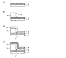
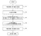
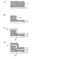
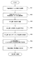
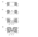
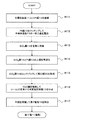
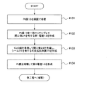
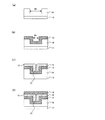
図1は、本実施形態における可変抵抗素子の製造方法を示す工程断面図であり、また図2は、該製造方法における工程手順を示すフローチャートであり、以下の文中の各ステップ#1〜#5は図2内の各ステップを表す。 FIG. 1 is a process cross-sectional view illustrating a method for manufacturing a variable resistance element according to the present embodiment, and FIG. 2 is a flowchart illustrating a process procedure in the manufacturing method. Represents each step in FIG.
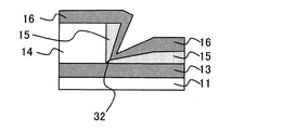
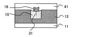
まず、図1(a)に示すように、トランジスタ回路等(図示せず)を適宜形成した半導体基板11上に導電性材料膜13(例えばPt膜)をスパッタ法にて約100nm程度の膜厚で全面に堆積する(ステップ#1)。本ステップ#1によって第1電極13が形成される。
First, as shown in FIG. 1A, a conductive material film 13 (for example, a Pt film) is formed on a
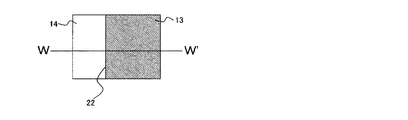
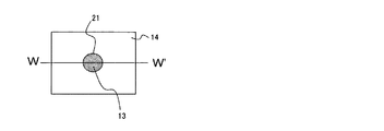
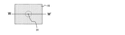
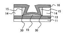
次に、絶縁性材料膜(例えばSiO2膜)14をCVD法(Chemical Vapor Deposition)法にて約300nm程度の膜厚で全面に堆積する(ステップ#2)。その後、公知のフォトリソグラフィ技術によって形成したレジストをマスクに、公知のエッチング技術によって、第1電極13の一部上面が露出するまでSiO2膜14をパターニングする(ステップ#3)。本ステップ#3によって、図1(b)に示すように、SiO2膜14(以下、適宜「絶縁膜14」という)の上面及び側面、並びに第1電極13の露出した上面によって段差部22が形成される。図3は、ステップ#3終了後の平面模式図であり、W−W’断面が、図1(b)に相当する。
Next, an insulating material film (for example, SiO 2 film) 14 is deposited on the entire surface with a film thickness of about 300 nm by the CVD method (Chemical Vapor Deposition) method (step # 2). Thereafter, using the resist formed by a known photolithography technique as a mask, the SiO 2 film 14 is patterned by a known etching technique until a partial upper surface of the
次に、図1(c)に示すように、段差部22が形成されている状態の下で、可変抵抗体膜15(例えばCoO膜)をスパッタ法にて約100nm程度の膜厚で全面に堆積する(ステップ#4)。本ステップ#4によって、段差部22で、絶縁膜14の側面と、露出した第1電極13の上面のそれぞれから成長する可変抵抗体膜としてのCoO膜15が接合する部分において、シーム32が形成される。
Next, as shown in FIG. 1C, under the state in which the
次に、図1(d)に示すように、シーム32が形成された可変抵抗体膜15の上面全面に導電性材料膜16(例えばPt膜)をスパッタ法にて約100nm程度の膜厚で堆積する(ステップ#5)。本ステップ#5によって第2電極16が形成される。
Next, as shown in FIG. 1D, a conductive material film 16 (for example, a Pt film) is formed on the entire upper surface of the
本実施形態によれば、ステップ#4に係る可変抵抗体膜成膜工程の直前において、既に段差部22(シーム形成用段差に相当)が形成されている。この段差部22は、基板11の基板面に平行な第1上面、基板面に平行に構成され前記第1上面より高さ位置の低い第2上面、並びに上端が前記第1上面の端部と結合し下端が前記第2上面の端部と結合することで前記第1上面と前記第2上面とを前記基板面に垂直な方向に連絡する中間面によって構成されている。そして、このうち、絶縁膜14の上面によって前記第1上面が構成され、絶縁膜14の側面によって前記中間面が構成され、第1電極13の露出した上面によって前記第2上面が構成される。
According to this embodiment, the step portion 22 (corresponding to a seam forming step) has already been formed immediately before the variable resistor film forming step according to
このような状態の下で、可変抵抗体膜としてのCoO膜を成膜することで、中間面(絶縁膜14の側面)から成長する膜と、第2上面(第1電極13の露出した上面)から成長する膜が接合する領域において、成長膜同士が重なり合うことでシーム32が形成される。このシーム32は、図1(c)に示すように、前記中間面と前記第2上面とが結合するコーナ領域から、露出した第1電極13の上面の上方に向かう方向に延伸する。
Under such a state, by forming a CoO film as a variable resistor film, a film grown from the intermediate surface (side surface of the insulating film 14) and a second upper surface (the exposed upper surface of the first electrode 13). ), The
そして、本発明の特徴として、このシーム32をそのまま残存させたまま、ステップ#5に係る第2電極形成工程を実行する。すなわち、第2電極16が形成された時点において、依然として可変抵抗体膜15内にはシーム32が形成されたままの状態となっている。また、前記のように、シーム32は、第1電極13と絶縁膜14によって挟まれたコーナ領域に形成されているところ、第1電極13から第2電極16に向かう方向に延伸するように形成されることとなる。
Then, as a feature of the present invention, the second electrode forming step according to
このようにシーム32が可変抵抗体膜15内に形成されたままの状態で、第1電極13と第2電極16の間に電圧パルスを印加した場合、シーム32では、バルクの可変抵抗体膜15に比べ構造欠陥が多いため電界集中が起こり易い。このため、フォーミングプロセスを行うべく電圧を印加したとき、電界集中が起こりやすいシーム内あるいはその近傍においてフィラメントパスが容易に形成しやすい状況となる。このため、予め製造時に特定箇所にシーム32を意図的に形成しておくことで、フォーミングプロセスによって形成されるフィラメントパスの形成領域を特定範囲内に収めることができ、スイッチング動作の再現性を高めることができる。さらに、シーム32内あるいはその近傍において電界集中が起こりやすい構成であるため、従来構成よりもフォーミングプロセス実行に要する電圧を低電圧化することができる。
When a voltage pulse is applied between the
また、シーム32は、必ずしも第1電極13と第2電極16の両者に接触するように形成される必要はなく、一方の電極のみに接触して形成されるものとしても構わないし、両電極に接触せず可変抵抗体13内に形成されるものとしても構わない。少なくとも可変抵抗体13内にシーム32が形成されていれば、当該シーム32形成領域においてフィラメントパスが容易に形成しやすくなるため、フィラメントパスの形成領域を特定することができるという効果を奏する。
The
なお、本実施形態において、第1電極13と第2電極16をともにPt膜としたが、電極としての機能を果たす材料であれば、Pt膜には限られず、例えば、AlやTiN等の他の導電性材料(金属を含む)であっても構わない。また、半導体基板11と第1電極13の間、および、可変抵抗体15と第2電極の間には、密着層として、例えば、Tiなどを用いてもよい。以下の各実施形態においても同様とする。
In this embodiment, the
また、絶縁膜14を本実施形態ではSiO2膜としたが、この絶縁体層はSiO2膜に限られたものではなく、SiN膜、SiON膜、SiOF膜、SiOC膜等の耐酸化性を有する任意の適切な絶縁膜を用いることが可能である。さらに、ステップ#2では、絶縁膜14をCVD法で堆積するものとしたが、パルス化レーザ堆積、rf−スパッタリング、電子ビーム蒸発、熱蒸発、スピンオン堆積等の任意の適切な堆積技術を用いて堆積することも可能である。以下の各実施形態においても、特に断らない限り同様とする。
In this embodiment, the insulating
また、本実施形態においてPt膜13を成膜する下地となる半導体基板11はトランジスタ回路等が適宜形成されているものとしたが、必ずしも当該回路が形成されている必要はない。以下の各実施形態においても同様とする。
In the present embodiment, the
さらに、本実施形態では、可変抵抗体膜15としてCoO膜を用いているが、可変抵抗性を示す材料であればCoOに限られるものではなく、例えば、Ti、V、Mn、Fe、Co、Ni、Zn、Zr、Nb、Hf、Ta、W等の金属の酸化物または酸窒化物を利用するものとしても構わない。以下の各実施形態においても同様とする。
Further, in this embodiment, a CoO film is used as the
なお、本実施形態では、ステップ#4に係る可変抵抗体膜成膜工程において、可変抵抗体膜としてのCoO膜を成膜するものとしたが、Co膜を全体に堆積した後、酸化処理を施すことでCoO膜を形成するものとしても構わない。このとき、堆積する材料膜は、可変抵抗体膜15として形成する材料に応じて適宜選択可能である。以下の各実施形態においても同様とする。
In this embodiment, the CoO film as the variable resistor film is formed in the variable resistor film forming process according to
また、特に段差部22の高さを100nm以上とし、ステップ#4に係る可変抵抗体膜成膜工程において、この段差部22がスパッタターゲットに対して背面位置となるような位置関係でスパッタを実行することで、より大きなシーム32を形成することが可能となる。以下の第2〜第12実施形態においても同様とする。
Further, in particular, the height of the stepped
[第2実施形態]
本発明に係る可変抵抗素子及びその製造方法、並びにその駆動方法の第2実施形態(以下、適宜「本実施形態」という)につき、図4〜図5の各図を参照して説明する。
[Second Embodiment]
A variable resistance element, a manufacturing method thereof, and a driving method thereof according to a second embodiment of the present invention (hereinafter, referred to as “this embodiment” as appropriate) will be described with reference to FIGS.
図4は、本実施形態における可変抵抗素子の製造方法を示す工程断面図である。また、図5は、該製造方法における工程手順を示すフローチャートであり、以下の文中の各ステップ#11〜#17は図5内の各ステップを表す。なお、第1実施形態と同一の構成要素には同一の符号を付している。
FIG. 4 is a process cross-sectional view illustrating the method of manufacturing the variable resistance element in the present embodiment. FIG. 5 is a flowchart showing a process procedure in the manufacturing method, and each
まず、トランジスタ回路等(図示せず)を適宜形成した半導体基板11上に絶縁性材料膜(例えばSiO2膜)14を堆積する(ステップ#11)。その後、SiO2膜14をエッチングして、半導体基板11の一部上面を露出させる(ステップ#12)。その後、導電性材料膜(例えばPt膜)13を全面に堆積した後(ステップ#13)、公知の平坦化技術を用いてSiO2膜14(以下、絶縁膜14という)とPt膜13の上面を露出させる(ステップ#14、図4(a)参照)。
First, an insulating material film (for example, SiO 2 film) 14 is deposited on a
なお、このとき、まず全面にPt膜13を堆積した後、Pt膜13をエッチングして半導体基板11の一部上面を露出させ、その後にSiO2膜14を全面に堆積した後、公知の平坦化技術を用いてSiO2膜14とPt膜13の上面を露出させるものとしても良い。
At this time, the
次に、公知のフォトリソグラフィ技術によって形成したレジストをマスクに、公知のエッチング技術によって、Pt膜13をエッチバックして段差部22を形成する(ステップ#15)。本ステップ#15によって、第1電極13が形成されるとともに、図4(b)に示すように、SiO2膜14(以下、適宜「絶縁膜14」という)の上面及び側面、並びに第1電極13の露出した上面によって段差部22が形成される。なお、本実施形態におけるステップ#15終了後の平面模式図は、図3に示す第1実施形態のステップ#3終了後の平面模式図と同一であり、W−W’断面が、図4(b)に相当する。
Next, using the resist formed by a known photolithography technique as a mask, the
その後は、図4(c)に示すように、第1実施形態のステップ#4と同様、段差部22が形成されている状態の下で、可変抵抗体膜15(例えばCoO膜)をスパッタ法にて約100nm程度の膜厚で全面に堆積する(ステップ#16)。本ステップ#16によって、段差部22で、絶縁膜14の側面と、第1電極13の上面のそれぞれから成長する可変抵抗体膜としてのCoO膜15が接合する部分において、シーム32が形成される。
Thereafter, as shown in FIG. 4C, as in
その後、図4(d)に示すように、第1実施形態のステップ#5と同様、シーム32が形成された可変抵抗体膜15の上面全面に導電性材料膜16(例えばPt膜)をスパッタ法にて約100nm程度の膜厚で堆積する(ステップ#17)。本ステップ#16によって第2電極16が形成される。
Thereafter, as shown in FIG. 4D, as in
本実施形態の場合も、第1実施形態と同様、ステップ#16に係る可変抵抗体膜成膜工程の直前において、既に段差部22(シーム形成用段差に相当)が形成されている。この段差部22は、基板11の基板面に平行な第1上面、基板面に平行に構成され前記第1上面より高さ位置の低い第2上面、並びに上端が前記第1上面の端部と結合し下端が前記第2上面の端部と結合することで前記第1上面と前記第2上面とを前記基板面に垂直な方向に連絡する中間面によって構成されている。そして、このうち、絶縁膜14の上面によって前記第1上面が構成され、絶縁膜14の側面によって前記中間面が構成され、第1電極13の露出した上面によって前記第2上面が構成される。
In the present embodiment as well, as in the first embodiment, the step portion 22 (corresponding to a seam forming step) has already been formed immediately before the variable resistor film forming step according to
このような状態の下で、可変抵抗体膜としてのCoO膜を成膜することで、中間面(絶縁膜14の側面)から成長する膜と、第2上面(第1電極13の露出した上面)から成長する膜が接合する領域において、成長膜同士が重なり合うことでシーム32が形成される。このシーム32は、図4(c)に示すように、前記中間面と前記第2上面とが結合するコーナ領域から、露出した第1電極13の上面の上方に向かう方向に延伸する。そして、このシーム32をそのまま残存させたまま、ステップ#17に係る第2電極形成工程を実行することで、第2電極16が形成された時点において、依然として可変抵抗体膜15内にはシーム32が形成されたままの状態となっている。また、前記のように、シーム32は、第1電極13と絶縁膜14によって挟まれたコーナ領域に形成されているところ、第1電極13から第2電極16に向かう方向に延伸するように形成されることとなる。
Under such a state, by forming a CoO film as a variable resistor film, a film grown from the intermediate surface (side surface of the insulating film 14) and a second upper surface (the exposed upper surface of the first electrode 13). ), The
従って、本実施形態の場合も、第1実施形態と同様、シーム32が可変抵抗体膜15内に形成されたままの状態で、第1電極13と第2電極16の間に電圧パルスを印加した場合、シーム32では、バルクの可変抵抗体膜15に比べ構造欠陥が多いため電界集中が起こり易い。このため、フォーミングプロセスを行うべく電圧を印加したとき、電界集中が起こりやすいシーム内あるいはその近傍においてフィラメントパスが容易に形成しやすい状況となる。このため、予め製造時に特定箇所にシーム32を意図的に形成しておくことで、フォーミングプロセスによって形成されるフィラメントパスの形成領域を特定範囲内に収めることができ、スイッチング動作の再現性を高めることができる。さらに、シーム32内あるいはその近傍において電界集中が起こりやすい構成であるため、従来構成よりもフォーミングプロセス実行に要する電圧を低電圧化することができる。以下の第3〜第6実施形態においても同様であるため、適宜説明を省略する。
Accordingly, in this embodiment as well, as in the first embodiment, a voltage pulse is applied between the
[第3実施形態]
本発明に係る可変抵抗素子及びその製造方法、並びにその駆動方法の第3実施形態(以下、適宜「本実施形態」という)につき、図6〜図8の各図を参照して説明する。
[Third Embodiment]
A third embodiment (hereinafter referred to as “this embodiment” as appropriate) of a variable resistance element, a manufacturing method thereof, and a driving method thereof according to the present invention will be described with reference to FIGS.
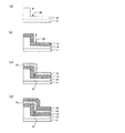
図6は、本実施形態における可変抵抗素子の製造方法を示す工程断面図である。また、図7は、該製造方法における工程手順を示すフローチャートであり、以下の文中の各ステップ#21〜#24は図7内の各ステップを表す。なお、第1実施形態と同一の構成要素には同一の符号を付している。
FIG. 6 is a process cross-sectional view illustrating the method of manufacturing the variable resistance element in the present embodiment. FIG. 7 is a flowchart showing a process procedure in the manufacturing method, and each
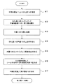
まず、図6(a)に示すように、トランジスタ回路等(図示せず)を適宜形成した半導体基板11上に導電性材料膜13(例えばPt膜)をスパッタ法にて約400nmの厚みで全面に堆積する(ステップ#21)。なお、本ステップ#21では、第1実施形態のステップ#1よりも厚い膜厚で堆積する。
First, as shown in FIG. 6A, a conductive material film 13 (for example, Pt film) is formed on the entire surface of a
次に、公知のフォトリソグラフィ技術によって形成したレジストをマスクに、公知のエッチング技術によって、Pt膜13に例えば高低差300nm程度の段差部25を形成する(ステップ#22)。本ステップ#22によって、第1電極13が形成されるとともに、図6(b)に示すように、高さ位置の高い第1電極13の上面、第1電極13の側面、並びに高さ位置の低い第1電極13の上面によって段差部25が形成される。図8は、ステップ#22終了後の平面模式図であり、W−W’断面が、図6(b)に相当する。
Next, a
その後は、図6(c)に示すように、第1実施形態のステップ#4と同様、段差部22(シーム形成用段差に相当)が形成されている状態の下で、可変抵抗体膜15(例えばCoO膜)をスパッタ法にて約100nm程度の膜厚で全面に堆積する(ステップ#23)。本ステップ#23によって、段差部25で、高さ位置の低い第1電極13の上面、及び第1電極13の側面のそれぞれから成長する可変抵抗体膜としてのCoO膜15が接合する部分において、シーム32が形成される。
Thereafter, as shown in FIG. 6C, the
その後、図6(d)に示すように、第1実施形態のステップ#5と同様、シーム32が形成された可変抵抗体膜15の上面全面に導電性材料膜16(例えばPt膜)をスパッタ法にて約100nm程度の膜厚で堆積する(ステップ#24)。本ステップ#16によって第2電極16が形成される。
Thereafter, as shown in FIG. 6D, as in
[第4実施形態]
本発明に係る可変抵抗素子及びその製造方法、並びにその駆動方法の第4実施形態(以下、適宜「本実施形態」という)につき、図9〜図10の各図を参照して説明する。
[Fourth Embodiment]
A variable resistance element, a manufacturing method thereof, and a driving method thereof according to a fourth embodiment of the present invention (hereinafter, referred to as “this embodiment” as appropriate) will be described with reference to FIGS.
図9は、本実施形態における可変抵抗素子の製造方法を示す工程断面図である。また、図10は、該製造方法における工程手順を示すフローチャートであり、以下の文中の各ステップ#31〜#35は図10内の各ステップを表す。 FIG. 9 is a process cross-sectional view illustrating the method of manufacturing the variable resistance element in the present embodiment. Moreover, FIG. 10 is a flowchart which shows the process sequence in this manufacturing method, and each step # 31- # 35 in the following sentences represents each step in FIG.
まず、トランジスタ回路等(図示せず)を適宜形成した半導体基板11上に絶縁性材料膜14(例えばSiO2膜)をスパッタ法にて例えば約400nm程度の膜厚で全面に堆積した後(ステップ#31)、公知のフォトリソグラフィ技術によって形成したレジストをマスクに、公知のエッチング技術によって、絶縁性材料膜14に例えば高低差300nm程度の段差部26を形成する(ステップ#32、図9(a)参照)。
First, an insulating material film 14 (for example, SiO 2 film) is deposited on the entire surface of the
次に、段差部26が形成されている絶縁性材料膜14(以下、適宜「絶縁膜14」という)の上層全面に導電性材料膜13(例えばPt膜)をスパッタ法にて約100nmの厚みで全面に堆積する(ステップ#33)。本ステップ#33によって、第1電極13が形成されるとともに、図9(b)に示すように、高さ位置の高い第1電極13の上面、第1電極13の側面、並びに高さ位置の低い第1電極13の上面によって段差部25が形成される。なお、本実施形態におけるステップ#33終了後の平面模式図は、図8に示す第3実施形態のステップ#22終了後の平面模式図と同一であり、W−W’断面が、図9(b)に相当する。
Next, a conductive material film 13 (for example, a Pt film) is deposited on the entire upper surface of the insulating material film 14 (hereinafter referred to as “insulating
その後は、図9(c)に示すように、第1実施形態のステップ#4と同様、段差部25(シーム形成用段差に相当)が形成されている状態の下で、可変抵抗体膜15(例えばCoO膜)をスパッタ法にて約100nm程度の膜厚で全面に堆積する(ステップ#34)。本ステップ#34によって、段差部25で、高さ位置の低い第1電極13の上面、及び第1電極13の側面のそれぞれから成長する可変抵抗体膜としてのCoO膜15が接合する部分において、シーム32が形成される。
After that, as shown in FIG. 9C, as in
その後、図9(d)に示すように、第1実施形態のステップ#5と同様、シーム32が形成された可変抵抗体膜15の上面全面に導電性材料膜16(例えばPt膜)をスパッタ法にて約100nm程度の膜厚で堆積する(ステップ#35)。本ステップ#35によって第2電極16が形成される。
Thereafter, as shown in FIG. 9D, as in
[第5実施形態]
本発明に係る可変抵抗素子及びその製造方法、並びにその駆動方法の第5実施形態(以下、適宜「本実施形態」という)につき、図11〜図12の各図を参照して説明する。
[Fifth Embodiment]
A variable resistance element, a manufacturing method thereof, and a driving method thereof according to a fifth embodiment of the present invention (hereinafter referred to as “this embodiment” as appropriate) will be described with reference to FIGS.
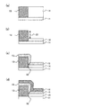
図11は、本実施形態における可変抵抗素子の製造方法を示す工程断面図である。また、図12は、該製造方法における工程手順を示すフローチャートであり、以下の文中の各ステップ#41〜#45は図12内の各ステップを表す。
FIG. 11 is a process cross-sectional view illustrating the method of manufacturing the variable resistance element in the present embodiment. FIG. 12 is a flowchart showing process steps in the manufacturing method.
まず、図11(a)に示すように、トランジスタ回路等(図示せず)を適宜形成した半導体基板11上に絶縁性材料膜14(例えばSiO2膜)をスパッタ法にて例えば約100nm程度の膜厚で全面に堆積する(ステップ#41)。
First, as shown in FIG. 11A, an insulating material film 14 (for example, SiO 2 film) is formed on a
次に、導電性材料膜13(例えばPt膜)をスパッタ法にて約300nm程度の膜厚で全面に堆積する(ステップ#42)。その後、公知のフォトリソグラフィ技術によって形成したレジストをマスクに、公知のエッチング技術によって、絶縁性材料膜14(以下、適宜「絶縁膜14」という)の一部上面が露出するまでPt膜13をパターニングする(ステップ#43)。本ステップ#43によって、第1電極13が形成されるとともに、図11(b)に示すように、第1電極13の上面及び側面、並びに絶縁膜14の露出した上面によって段差部22が形成される。図13は、ステップ#43終了後の平面模式図であり、W−W’断面が、図11(b)に相当する。
Next, a conductive material film 13 (for example, a Pt film) is deposited on the entire surface with a film thickness of about 300 nm by a sputtering method (step # 42). Thereafter, using a resist formed by a known photolithography technique as a mask, the
その後は、図11(c)に示すように、第1実施形態のステップ#4と同様、段差部22(シーム形成用段差に相当)が形成されている状態の下で、可変抵抗体膜15(例えばCoO膜)をスパッタ法にて約100nm程度の膜厚で全面に堆積する(ステップ#44)。本ステップ#34によって、段差部22で、第1電極13の側面、及び絶縁膜14の上面のそれぞれから成長する可変抵抗体膜としてのCoO膜15が接合する部分において、シーム32が形成される。
After that, as shown in FIG. 11C, as in
その後、図11(d)に示すように、第1実施形態のステップ#5と同様、シーム32が形成された可変抵抗体膜15の上面全面に導電性材料膜16(例えばPt膜)をスパッタ法にて約100nm程度の膜厚で堆積する(ステップ#45)。本ステップ#45によって第2電極16が形成される。
Thereafter, as shown in FIG. 11D, as in
[第6実施形態]
本発明に係る可変抵抗素子及びその製造方法、並びにその駆動方法の第6実施形態(以下、適宜「本実施形態」という)につき、図14〜図15の各図を参照して説明する。
[Sixth Embodiment]
A variable resistance element according to the present invention, a manufacturing method thereof, and a driving method thereof according to a sixth embodiment (hereinafter referred to as “this embodiment” as appropriate) will be described with reference to FIGS.
図14は、本実施形態における可変抵抗素子の製造方法を示す工程断面図である。また、図15は、該製造方法における工程手順を示すフローチャートであり、以下の文中の各ステップ#51〜#57は図14内の各ステップを表す。
FIG. 14 is a process cross-sectional view illustrating the variable resistance element manufacturing method according to the present embodiment. FIG. 15 is a flowchart showing a process procedure in the manufacturing method, and each
まず、トランジスタ回路等(図示せず)を適宜形成した半導体基板11上に導電性材料膜(例えばPt膜)13を堆積形成する(ステップ#51)。その後、Pt膜13をエッチングして、半導体基板11の一部上面を露出させるとともに第1電極13を形成する(ステップ#52)。その後、絶縁性材料膜(例えばSiO2膜)14を全面に堆積した後(ステップ#53)、公知の平坦化技術を用いてSiO2膜14(以下、絶縁膜14という)と第1電極13の上面を露出させる(ステップ#54、図14(a)参照)。
First, a conductive material film (for example, Pt film) 13 is deposited and formed on a
なお、このとき、まず全面にSiO2膜14を堆積した後、SiO2膜14をエッチングして半導体基板11の一部上面を露出させ、その後にPt膜13を全面に堆積した後、公知の平坦化技術を用いてSiO2膜14とPt膜13の上面を露出させるものとしても良い。
At this time, the SiO 2 film 14 is first deposited on the entire surface, then the SiO 2 film 14 is etched to expose a part of the upper surface of the
次に、公知のフォトリソグラフィ技術によって形成したレジストをマスクに、公知のエッチング技術によって、SiO2膜14をエッチバックして段差部22を形成する(ステップ#55)。本ステップ#55によって、図14(b)に示すように、第1電極13の上面及び側面、並びにSiO2膜14(以下、適宜「絶縁膜14」という)の露出した上面によって段差部22が形成される。なお、本実施形態におけるステップ#55終了後の平面模式図は、図13に示す第5実施形態のステップ#43終了後の平面模式図と同一であり、W−W’断面が、図14(b)に相当する。
Next, using the resist formed by a known photolithography technique as a mask, the
その後は、図14(c)に示すように、第1実施形態のステップ#4と同様、段差部22(シーム形成用段差に相当)が形成されている状態の下で、可変抵抗体膜15(例えばCoO膜)をスパッタ法にて約100nm程度の膜厚で全面に堆積する(ステップ#56)。本ステップ#56によって、段差部22で、第1電極13の側面と、絶縁膜14の上面のそれぞれから成長する可変抵抗体膜としてのCoO膜15が接合する部分において、シーム32が形成される。
After that, as shown in FIG. 14C, the
その後、図14(d)に示すように、第1実施形態のステップ#5と同様、シーム32が形成された可変抵抗体膜15の上面全面に導電性材料膜16(例えばPt膜)をスパッタ法にて約100nm程度の膜厚で堆積する(ステップ#57)。本ステップ#57によって第2電極16が形成される。
Thereafter, as shown in FIG. 14D, as in
[第7実施形態]
本発明に係る可変抵抗素子及びその製造方法、並びにその駆動方法の第6実施形態(以下、適宜「本実施形態」という)につき、図16〜図18の各図を参照して説明する。
[Seventh Embodiment]
A sixth embodiment (hereinafter referred to as “this embodiment” as appropriate) of a variable resistance element, a manufacturing method thereof, and a driving method thereof according to the present invention will be described with reference to FIGS.
図16は、本実施形態における可変抵抗素子の製造方法を示す工程断面図である。また、図17は、該製造方法における工程手順を示すフローチャートであり、以下の文中の各ステップ#61〜#65は図17内の各ステップを表す。なお、第1実施形態と同一の構成要素には同一の符号を付している。 FIG. 16 is a process cross-sectional view illustrating the method of manufacturing the variable resistance element in the present embodiment. FIG. 17 is a flowchart showing a process procedure in the manufacturing method, and steps # 61 to # 65 in the following sentence represent steps in FIG. In addition, the same code | symbol is attached | subjected to the component same as 1st Embodiment.
まず、図16(a)に示すように、トランジスタ回路等(図示せず)を適宜形成した半導体基板11上に導電性材料膜13(例えばPt膜)をスパッタ法にて約100nm程度の膜厚で全面に堆積する(ステップ#61)。本ステップ#61によって第1電極13が形成される。
First, as shown in FIG. 16A, a conductive material film 13 (for example, Pt film) is formed on a
次に、絶縁性材料膜(例えばSiO2膜)14をCVD法にて約300nm程度の膜厚で全面に堆積する(ステップ#62)。その後、公知のフォトリソグラフィ技術によって形成したレジストをマスクに、公知のエッチング技術によって、第1電極13の一部上面が露出するまでSiO2膜14をパターニングする(ステップ#63)。本ステップ#63によって、図16(b)に示すように、露出した第1電極13の上面を底面とし、SiO2膜14(以下、適宜「絶縁膜14」という)の側面を内側面とする開口部20が形成される。図18は、ステップ#63終了後の平面模式図であり、W−W’断面が、図16(b)に相当する。
Next, an insulating material film (for example, SiO 2 film) 14 is deposited on the entire surface with a thickness of about 300 nm by the CVD method (step # 62). Thereafter, using the resist formed by a known photolithography technique as a mask, the SiO 2 film 14 is patterned by a known etching technique until a partial upper surface of the
次に、図16(c)に示すように、開口部20が形成されている状態の下で、可変抵抗体膜15(例えばCoO膜)をスパッタ法にて、開口部20内を完全には充填しない膜厚条件下(例えば約100nm程度)の膜厚で全面に堆積する(ステップ#64)。本ステップ#64によって、開口部20の内側面を構成する絶縁膜14の側面と、開口部20の底面を構成する露出した第1電極13の上面のそれぞれから成長する可変抵抗体膜としてのCoO膜15が接合する部分において、シーム30が形成される。
Next, as shown in FIG. 16C, the variable resistor film 15 (for example, a CoO film) is completely sputtered in the
次に、図16(d)に示すように、シーム30が形成された可変抵抗体膜15の上面全面に導電性材料膜16(例えばPt膜)をスパッタ法にて約100nm程度の膜厚で堆積する(ステップ#65)。本ステップ#65によって第2電極16が形成される。
Next, as shown in FIG. 16D, a conductive material film 16 (for example, a Pt film) is formed on the entire upper surface of the
本実施形態の場合、ステップ#64に係る可変抵抗体膜成膜工程の直前において、既に開口部20(シーム形成用開口部に相当)が形成されている。この開口部20は、前記基板面に平行な断面が環状に形成された露出内側面、前記露出内側面の外側において前記露出内側面の上端と端部が結合する第1上面、並びに前記露出内側面の内側において前記露出内側面の下端と端部が結合する露出底面によって構成されている。そして、このうち、絶縁膜14の上面によって前記第1上面が構成され、絶縁膜14の側面によって前記露出内側面が構成され、第1電極13の露出した上面によって前記露出底面が構成される。
In the present embodiment, the opening 20 (corresponding to the seam forming opening) has already been formed immediately before the variable resistor film forming step according to
このような状態の下で、可変抵抗体膜としてのCoO膜を成膜することで、露出内側面(絶縁膜14の側面)から成長する膜と、露出底面(第1電極13の露出した上面)から成長する膜が接合する領域において、成長膜同士が重なり合うことでシーム30が形成される。このシーム30は、図16(c)に示すように、前記露出内側面と前記露出底面とが結合するコーナ領域から、露出した第1電極13の上面の上方に向かう方向に延伸する。そして、このシーム30をそのまま残存させたまま、ステップ#65に係る第2電極形成工程を実行することで、第2電極16が形成された時点において、依然として可変抵抗体膜15内にはシーム30が形成されたままの状態となっている。また、前記のように、シーム30は、第1電極13と絶縁膜14によって挟まれたコーナ領域に形成されているところ、第1電極13から第2電極16に向かう方向に延伸するように形成されることとなる。
Under such a state, by forming a CoO film as a variable resistor film, a film grown from the exposed inner surface (side surface of the insulating film 14) and an exposed bottom surface (exposed upper surface of the first electrode 13). ), The
従って、本実施形態の場合も、第1実施形態と同様、シーム30が可変抵抗体膜15内に形成されたままの状態で、第1電極13と第2電極16の間に電圧パルスを印加した場合、シーム30では、バルクの可変抵抗体膜15に比べ構造欠陥が多いため電界集中が起こり易い。このため、フォーミングプロセスを行うべく電圧を印加したとき、電界集中が起こりやすいシーム内あるいはその近傍においてフィラメントパスが容易に形成しやすい状況となる。このため、予め製造時に特定箇所にシーム30を意図的に形成しておくことで、フォーミングプロセスによって形成されるフィラメントパスの形成領域を特定範囲内に収めることができ、スイッチング動作の再現性を高めることができる。さらに、シーム30内あるいはその近傍において電界集中が起こりやすい構成であるため、従来構成よりもフォーミングプロセス実行に要する電圧を低電圧化することができる。以下の第8〜第12実施形態においても同様であるため、適宜説明を省略する。
Accordingly, in the present embodiment as well, as in the first embodiment, a voltage pulse is applied between the
[第8実施形態]
本発明に係る可変抵抗素子及びその製造方法、並びにその駆動方法の第8実施形態(以下、適宜「本実施形態」という)につき、図19〜図20の各図を参照して説明する。
[Eighth Embodiment]
An eighth embodiment (hereinafter referred to as “this embodiment” as appropriate) of a variable resistance element, a manufacturing method thereof, and a driving method thereof according to the present invention will be described with reference to FIGS. 19 to 20.
図19は、本実施形態における可変抵抗素子の製造方法を示す工程断面図である。また、図20は、該製造方法における工程手順を示すフローチャートであり、以下の文中の各ステップ#71〜#77は図20内の各ステップを表す。なお、第1実施形態と同一の構成要素には同一の符号を付している。
FIG. 19 is a process cross-sectional view illustrating the variable resistance element manufacturing method according to the present embodiment. FIG. 20 is a flowchart showing process steps in the manufacturing method.
まず、第2実施形態のステップ#11〜ステップ#14と同様に、トランジスタ回路等(図示せず)を適宜形成した半導体基板11上に絶縁性材料膜(例えばSiO2膜)14を堆積し(ステップ#71)、SiO2膜14をエッチングして、半導体基板11の一部上面を露出させ(ステップ#72)、導電性材料膜(例えばPt膜)13を全面に堆積した後(ステップ#73)、公知の平坦化技術を用いてSiO2膜14(以下、絶縁膜14という)とPt膜13の上面を露出させる(ステップ#74、図19(a)参照)。このとき、まず全面にPt膜13を堆積した後、Pt膜13をエッチングして半導体基板11の一部上面を露出させ、その後にSiO2膜14を全面に堆積した後、公知の平坦化技術を用いてSiO2膜14とPt膜13の上面を露出させるものとしても良い。
First, as in
次に、公知のフォトリソグラフィ技術によって形成したレジストをマスクに、公知のエッチング技術によって、Pt膜13をエッチバックして開口部20を形成する(ステップ#75)。本ステップ#75によって、第1電極13が形成されるとともに、図19(b)に示すように、SiO2膜14(以下、適宜「絶縁膜14」という)の上面及び側面、並びに第1電極13の露出した上面によって開口部20が形成される。より具体的には、露出した第1電極13を底面とし、絶縁膜14を内側面とする開口部20が形成される。なお、本実施形態におけるステップ#75終了後の平面模式図は、図18に示す第7実施形態のステップ#63終了後の平面模式図と同一であり、W−W’断面が、図19(b)に相当する。
Next, using the resist formed by a known photolithography technique as a mask, the
その後は、図19(c)に示すように、第7実施形態のステップ#64と同様、開口部20(シーム形成用開口部に相当)が形成されている状態の下で、可変抵抗体膜15(例えばCoO膜)をスパッタ法にて開口部20内を完全には充填しない膜厚条件下(例えば約100nm程度)の膜厚で全面に堆積する(ステップ#76)。本ステップ#76によって、開口部20の内側面を構成する絶縁膜14の側面と、開口部20の底面を構成する第1電極13の上面のそれぞれから成長する可変抵抗体膜としてのCoO膜15が接合する部分において、シーム30が形成される。
After that, as shown in FIG. 19C, the variable resistor film is formed under the state in which the opening 20 (corresponding to the seam forming opening) is formed as in
その後、図19(d)に示すように、第7実施形態のステップ#65と同様、シーム30が形成された可変抵抗体膜15の上面全面に導電性材料膜16(例えばPt膜)をスパッタ法にて約100nm程度の膜厚で堆積する(ステップ#77)。本ステップ#77によって第2電極16が形成される。
Thereafter, as shown in FIG. 19D, as in
[第9実施形態]
本発明に係る可変抵抗素子及びその製造方法、並びにその駆動方法の第9実施形態(以下、適宜「本実施形態」という)につき、図21〜図23の各図を参照して説明する。
[Ninth Embodiment]
A ninth embodiment (hereinafter referred to as “this embodiment” as appropriate) of a variable resistance element, a manufacturing method thereof, and a driving method thereof according to the present invention will be described with reference to FIGS.
図21は、本実施形態における可変抵抗素子の製造方法を示す工程断面図である。また、図22は、該製造方法における工程手順を示すフローチャートであり、以下の文中の各ステップ#81〜#84は図22内の各ステップを表す。なお、第1実施形態と同一の構成要素には同一の符号を付している。 FIG. 21 is a process cross-sectional view illustrating the method of manufacturing the variable resistance element in the present embodiment. FIG. 22 is a flowchart showing a process procedure in the manufacturing method, and steps # 81 to # 84 in the following sentence represent steps in FIG. In addition, the same code | symbol is attached | subjected to the component same as 1st Embodiment.
まず、図21(a)に示すように、第3実施形態のステップ#21と同様、トランジスタ回路等(図示せず)を適宜形成した半導体基板11上に導電性材料膜13(例えばPt膜)をスパッタ法にて約400nmの厚みで全面に堆積する(ステップ#81)。
First, as shown in FIG. 21A, like
次に、公知のフォトリソグラフィ技術によって形成したレジストをマスクに、公知のエッチング技術によって、Pt膜13に例えば高低差300nm程度の開口部23を形成する(ステップ#82)。本ステップ#82によって、第1電極13が形成されるとともに、図21(b)に示すように、第1電極13の側面を内側面とし、高さ位置の低い第1電極13の上面を底面とする開口部23が形成される。図23は、ステップ#82終了後の平面模式図であり、W−W’断面が、図21(b)に相当する。
Next, an
その後は、図21(c)に示すように、第7実施形態のステップ#64と同様、開口部23(シーム形成用開口部に相当)が形成されている状態の下で、可変抵抗体膜15(例えばCoO膜)をスパッタ法にて開口部23内を完全には充填しない膜厚条件下(例えば約100nm程度)の膜厚で全面に堆積する(ステップ#83)。本ステップ#83によって、開口部23の内側面を構成する第1電極13の側面と、開口部23の底面を構成する第1電極13の高さ位置の低い側の上面のそれぞれから成長する可変抵抗体膜としてのCoO膜15が接合する部分において、シーム30が形成される。
After that, as shown in FIG. 21C, the variable resistor film is formed under the state in which the opening 23 (corresponding to the seam forming opening) is formed, as in
その後、図21(d)に示すように、第7実施形態のステップ#65と同様、シーム30が形成された可変抵抗体膜15の上面全面に導電性材料膜16(例えばPt膜)をスパッタ法にて約100nm程度の膜厚で堆積する(ステップ#84)。本ステップ#84によって第2電極16が形成される。
After that, as shown in FIG. 21D, the conductive material film 16 (for example, Pt film) is sputtered on the entire upper surface of the
[第10実施形態]
本発明に係る可変抵抗素子及びその製造方法、並びにその駆動方法の第9実施形態(以下、適宜「本実施形態」という)につき、図24〜図25の各図を参照して説明する。
[Tenth embodiment]
A ninth embodiment (hereinafter referred to as “this embodiment” as appropriate) of a variable resistance element, a manufacturing method thereof, and a driving method thereof according to the present invention will be described with reference to FIGS.
図24は、本実施形態における可変抵抗素子の製造方法を示す工程断面図である。また、図25は、該製造方法における工程手順を示すフローチャートであり、以下の文中の各ステップ#91〜#95は図25内の各ステップを表す。なお、第1実施形態と同一の構成要素には同一の符号を付している。
FIG. 24 is a process cross-sectional view illustrating the method of manufacturing the variable resistance element in the present embodiment. FIG. 25 is a flowchart showing a process procedure in the manufacturing method.
まず、トランジスタ回路等(図示せず)を適宜形成した半導体基板11上に絶縁性材料膜14(例えばSiO2膜)をスパッタ法にて例えば約400nm程度の膜厚で全面に堆積した後(ステップ#91)、公知のフォトリソグラフィ技術によって形成したレジストをマスクに、公知のエッチング技術によって、絶縁性材料膜14に例えば高低差300nm程度の開口部29を形成する(ステップ#92、図24(a)参照)。
First, an insulating material film 14 (for example, SiO 2 film) is deposited on the entire surface of the
次に、開口部29が形成されている絶縁性材料膜14(以下、適宜「絶縁膜14」という)の上層全面に導電性材料膜13(例えばPt膜)をスパッタ法にて約100nmの厚みで全面に堆積する(ステップ#93)。本ステップ#93によって、図24(b)に示すように、Pt膜13(以下、第1電極13という)の側面を内側面とし、高さ位置の低い第1電極13の上面を底面とする開口部23が形成される。なお、本実施形態におけるステップ#93終了後の平面模式図は、図23に示す第9実施形態のステップ#82終了後の平面模式図と同一であり、W−W’断面が、図24(b)に相当する。
Next, a conductive material film 13 (for example, a Pt film) is formed on the entire upper surface of the insulating material film 14 (hereinafter referred to as “insulating
その後は、図24(c)に示すように、第7実施形態のステップ#64と同様、開口部23(シーム形成用開口部に相当)が形成されている状態の下で、可変抵抗体膜15(例えばCoO膜)をスパッタ法にて開口部23内を完全には充填しない膜厚条件下(例えば約100nm程度)の膜厚で全面に堆積する(ステップ#94)。本ステップ#94によって、開口部23の内側面を構成する第1電極13の側面と、開口部23の底面を構成する第1電極13の高さ位置の低い側の上面のそれぞれから成長する可変抵抗体膜としてのCoO膜15が接合する部分において、シーム30が形成される。
After that, as shown in FIG. 24C, the variable resistor film is formed under the state in which the opening 23 (corresponding to the seam forming opening) is formed as in
その後、図24(d)に示すように、第7実施形態のステップ#65と同様、シーム30が形成された可変抵抗体膜15の上面全面に導電性材料膜16(例えばPt膜)をスパッタ法にて約100nm程度の膜厚で堆積する(ステップ#95)。本ステップ#95によって第2電極16が形成される。
Thereafter, as shown in FIG. 24D, as in
[第11実施形態]
本発明に係る可変抵抗素子及びその製造方法、並びにその駆動方法の第9実施形態(以下、適宜「本実施形態」という)につき、図26〜図28の各図を参照して説明する。
[Eleventh embodiment]
A ninth embodiment (hereinafter, referred to as “this embodiment” as appropriate) of a variable resistance element, a manufacturing method thereof, and a driving method thereof according to the present invention will be described with reference to FIGS.
図26は、本実施形態における可変抵抗素子の製造方法を示す工程断面図である。また、図27は、該製造方法における工程手順を示すフローチャートであり、以下の文中の各ステップ#101〜#105は図27内の各ステップを表す。なお、第1実施形態と同一の構成要素には同一の符号を付している。 FIG. 26 is a process cross-sectional view illustrating the method for manufacturing the variable resistance element according to this embodiment. FIG. 27 is a flowchart showing a process procedure in the manufacturing method. Steps # 101 to # 105 in the following sentence represent steps in FIG. In addition, the same code | symbol is attached | subjected to the component same as 1st Embodiment.
まず、図26(a)に示すように、第5実施形態のステップ#41と同様、トランジスタ回路等(図示せず)を適宜形成した半導体基板11上に絶縁性材料膜14(例えばSiO2膜)をスパッタ法にて例えば約100nm程度の膜厚で全面に堆積する(ステップ#101)。
First, as shown in FIG. 26A, as in
次に、導電性材料膜13(例えばPt膜)をスパッタ法にて約300nm程度の膜厚で全面に堆積した後(ステップ#102)、公知のフォトリソグラフィ技術によって形成したレジストをマスクに、公知のエッチング技術によって、絶縁性材料膜14(以下、適宜「絶縁膜14」という)の一部上面が露出するまでPt膜13をパターニングする(ステップ#103)ことで、開口部20を形成する。本ステップ#103によって、図26(b)に示すように、Pt膜13(以下、適宜「第1電極13」という)の側面を内側面とし、絶縁膜14の露出した上面を底面とする開口部20が形成される。図28は、ステップ#103終了後の平面模式図であり、W−W’断面が、図26(b)に相当する。
Next, a conductive material film 13 (for example, a Pt film) is deposited on the entire surface with a film thickness of about 300 nm by a sputtering method (step # 102), and then a resist formed by a known photolithography technique is used as a mask. By using this etching technique, the
その後は、図26(c)に示すように、第7実施形態のステップ#64と同様、開口部20(シーム形成用開口部に相当)が形成されている状態の下で、可変抵抗体膜15(例えばCoO膜)をスパッタ法にて開口部20内を完全には充填しない膜厚条件下(例えば約100nm程度)の膜厚で全面に堆積する(ステップ#104)。本ステップ#104によって、開口部20の内側面を構成する第1電極13の側面と、開口部20の底面を構成する絶縁膜14の露出した上面のそれぞれから成長する可変抵抗体膜としてのCoO膜15が接合する部分において、シーム30が形成される。
Thereafter, as shown in FIG. 26 (c), the variable resistor film is formed under the state in which the opening 20 (corresponding to the seam forming opening) is formed as in
その後、図26(d)に示すように、第7実施形態のステップ#65と同様、シーム30が形成された可変抵抗体膜15の上面全面に導電性材料膜16(例えばPt膜)をスパッタ法にて約100nm程度の膜厚で堆積する(ステップ#105)。本ステップ#105によって第2電極16が形成される。
Thereafter, as shown in FIG. 26D, as in
[第12実施形態]
本発明に係る可変抵抗素子及びその製造方法、並びにその駆動方法の第12実施形態(以下、適宜「本実施形態」という)につき、図29〜図30の各図を参照して説明する。
[Twelfth embodiment]
A twelfth embodiment (hereinafter referred to as “this embodiment” as appropriate) of a variable resistance element, a manufacturing method thereof, and a driving method thereof according to the present invention will be described with reference to FIGS.
図29は、本実施形態における可変抵抗素子の製造方法を示す工程断面図である。また、図30は、該製造方法における工程手順を示すフローチャートであり、以下の文中の各ステップ#111〜#117は図30内の各ステップを表す。 FIG. 29 is a process cross-sectional view illustrating the method for manufacturing the variable resistance element according to the present embodiment. FIG. 30 is a flowchart showing a process procedure in the manufacturing method, and steps # 111 to # 117 in the following sentence represent steps in FIG.
まず、第6実施形態のステップ#51〜#54と同様、トランジスタ回路等(図示せず)を適宜形成した半導体基板11上に導電性材料膜(例えばPt膜)13を堆積形成し(ステップ#111)、Pt膜13をエッチングして、半導体基板11の一部上面を露出させるとともに第1電極13を形成し(ステップ#112)、絶縁性材料膜(例えばSiO2膜)14を全面に堆積した後(ステップ#113)、公知の平坦化技術を用いてSiO2膜14(以下、絶縁膜14という)と第1電極13の上面を露出させる(ステップ#114、図29(a)参照)。
First, similarly to steps # 51 to # 54 of the sixth embodiment, a conductive material film (for example, Pt film) 13 is deposited on a
なお、このとき、まず全面にSiO2膜14を堆積した後、SiO2膜14をエッチングして半導体基板11の一部上面を露出させ、その後にPt膜13を全面に堆積した後、公知の平坦化技術を用いてSiO2膜14とPt膜13の上面を露出させるものとしても良い。
At this time, the SiO 2 film 14 is first deposited on the entire surface, then the SiO 2 film 14 is etched to expose a part of the upper surface of the
次に、公知のフォトリソグラフィ技術によって形成したレジストをマスクに、公知のエッチング技術によって、SiO2膜14をエッチバックして開口部20を形成する(ステップ#115)。本ステップ#115によって、図29(b)に示すように、第1電極13の側面を内側面とし、並びにSiO2膜14(以下、適宜「絶縁膜14」という)の露出した上面を底面とする開口部20が形成される。なお、本実施形態におけるステップ#115終了後の平面模式図は、図28に示す第11実施形態のステップ#103終了後の平面模式図と同一であり、W−W’断面が、図29(b)に相当する。
Next, using the resist formed by a known photolithography technique as a mask, the SiO 2 film 14 is etched back by a known etching technique to form an opening 20 (step # 115). In this
その後は、図29(c)に示すように、第7実施形態のステップ#64と同様、開口部20(シーム形成用開口部に相当)が形成されている状態の下で、可変抵抗体膜15(例えばCoO膜)をスパッタ法にて開口部20内を完全には充填しない膜厚条件下(例えば約100nm程度)の膜厚で全面に堆積する(ステップ#116)。本ステップ#116によって、開口部20の内側面を構成する第1電極13の側面と、開口部20の底面を構成する絶縁膜14の露出した上面のそれぞれから成長する可変抵抗体膜としてのCoO膜15が接合する部分において、シーム30が形成される。
Thereafter, as shown in FIG. 29 (c), the variable resistor film is formed under the condition that the opening 20 (corresponding to the seam forming opening) is formed, as in
その後、図29(d)に示すように、第7実施形態のステップ#65と同様、シーム30が形成された可変抵抗体膜15の上面全面に導電性材料膜16(例えばPt膜)をスパッタ法にて約100nm程度の膜厚で堆積する(ステップ#117)。本ステップ#117によって第2電極16が形成される。
Thereafter, as shown in FIG. 29 (d), as in
[第13実施形態]
本発明に係る可変抵抗素子及びその製造方法、並びにその駆動方法の第13実施形態(以下、適宜「本実施形態」という)につき、図31〜図34の各図を参照して説明する。
[Thirteenth embodiment]
A thirteenth embodiment (hereinafter referred to as “this embodiment” as appropriate) of a variable resistance element, a manufacturing method thereof, and a driving method thereof according to the present invention will be described with reference to FIGS.
図31は、本実施形態における可変抵抗素子の製造方法を示す工程断面図である。また、図32は、該製造方法における工程手順を示すフローチャートであり、以下の文中の各ステップ#121〜#125は図32内の各ステップを表す。なお、第1実施形態と同一の構成要素には同一の符号を付している。
FIG. 31 is a process cross-sectional view illustrating the method for manufacturing the variable resistance element according to the present embodiment. FIG. 32 is a flowchart showing a process procedure in the manufacturing method, and each
まず、図31(a)に示すように、トランジスタ回路等(図示せず)を適宜形成した半導体基板11上に導電性材料膜13(例えばPt膜)をスパッタ法にて約100nm程度の膜厚で全面に堆積する(ステップ#121)。本ステップ#121によって第1電極13が形成される。
First, as shown in FIG. 31A, a conductive material film 13 (for example, Pt film) is formed on a
次に、絶縁性材料膜(例えばSiO2膜)14をCVD法にて約300nm程度の膜厚で全面に堆積する(ステップ#122)。その後、公知のフォトリソグラフィ技術によって形成したレジストをマスクに、公知のエッチング技術によって、第1電極13の一部上面が露出するまでSiO2膜14をパターニングする(ステップ#123)。本ステップ#123によって、図31(b)に示すように、露出した第1電極13の上面を底面とし、SiO2膜14(以下、適宜「絶縁膜14」という)の側面を内側面とする開口部21が形成される。図33は、ステップ#123終了後の平面模式図であり、W−W’断面が、図31(b)に相当する。
Next, an insulating material film (for example, SiO 2 film) 14 is deposited on the entire surface with a film thickness of about 300 nm by the CVD method (step # 122). Thereafter, using the resist formed by a known photolithography technique as a mask, the SiO 2 film 14 is patterned by a known etching technique until a partial upper surface of the
次に、図31(c)に示すように、開口部21が形成されている状態の下で、可変抵抗体膜15(例えばCoO膜)をLP(Low Pressure)−CVD法にて、開口部21内を完全に充填するような膜厚条件下で全面に堆積する(ステップ#124)。本ステップ#124によって、開口部21の内側面を構成する絶縁膜14の側面から開口部21の軸心方向に成長する可変抵抗体膜としてのCoO膜15が接合する部分において、高さ方向(鉛直方向)に延伸するシーム31が形成される。図33は、ステップ#124終了後の平面模式図であり、W−W’断面が、図31(c)に相当する。
Next, as shown in FIG. 31C, the variable resistor film 15 (for example, a CoO film) is formed by the LP (Low Pressure) -CVD method in a state where the
その後、図31(d)に示すように、シーム31が形成された可変抵抗体膜15の上面全面に導電性材料膜16(例えばPt膜)をスパッタ法にて約100nm程度の膜厚で堆積する(ステップ#125)。本ステップ#125によって第2電極16が形成される。
Thereafter, as shown in FIG. 31D, a conductive material film 16 (for example, a Pt film) is deposited on the entire upper surface of the
本実施形態の場合も、第7実施形態と同様、ステップ#124に係る可変抵抗体膜成膜工程の直前において、既に開口部21(シーム形成用開口部に相当)が形成されている。この開口部21は、前記基板面に平行な断面が環状に形成された露出内側面、前記露出内側面の外側において前記露出内側面の上端と端部が結合する第1上面、並びに前記露出内側面の内側において前記露出内側面の下端と端部が結合する露出底面によって構成されている。そして、このうち、絶縁膜14の上面によって前記第1上面が構成され、絶縁膜14の側面によって前記露出内側面が構成され、第1電極13の露出した上面によって前記露出底面が構成される。
Also in the present embodiment, as in the seventh embodiment, the opening 21 (corresponding to the seam forming opening) has already been formed immediately before the variable resistor film forming step according to
このような状態の下で、可変抵抗体膜としてのCoO膜をCVD法で成膜することで、露出内側面(絶縁膜14の側面)から成長する膜と、露出底面(第1電極13の露出した上面)から成長する膜が接合する領域において、成長膜同士が重なり合うことでシーム31が形成される。CVD法によって可変抵抗体膜を成膜することで、下地面(開口部21の内側面及び底面)に沿って均一に膜成長し、この結果、図31(c)に示すように、開口部21の軸心近傍において、高さ方向(鉛直方向)に延伸するようにシーム31が形成される。そして、このシーム31をそのまま残存させたまま、ステップ#125に係る第2電極形成工程を実行することで、第2電極16が形成された時点において、依然として可変抵抗体膜15内にはシーム31が形成されたままの状態となっている。また、前記のように、シーム31は、軸心近傍において鉛直方向に延伸するように形成されているところ、第1電極13から第2電極16に向かう方向に延伸するように形成されることとなる。
Under such a state, a CoO film as a variable resistor film is formed by a CVD method, so that a film grown from the exposed inner surface (side surface of the insulating film 14) and an exposed bottom surface (first electrode 13) are formed. The
従って、本実施形態の場合も、第1実施形態と同様、シーム31が可変抵抗体膜15内に形成されたままの状態で、第1電極13と第2電極16の間に電圧パルスを印加した場合、シーム31では、バルクの可変抵抗体膜15に比べ構造欠陥が多いため電界集中が起こり易い。このため、フォーミングプロセスを行うべく電圧を印加したとき、電界集中が起こりやすいシーム内あるいはその近傍においてフィラメントパスが容易に形成しやすい状況となる。このため、予め製造時に特定箇所にシーム31を意図的に形成しておくことで、フォーミングプロセスによって形成されるフィラメントパスの形成領域を特定範囲内に収めることができ、スイッチング動作の再現性を高めることができる。さらに、シーム31内あるいはその近傍において電界集中が起こりやすい構成であるため、従来構成よりもフォーミングプロセス実行に要する電圧を低電圧化することができる。以下の第14〜第15実施形態においても同様であるため、適宜説明を省略する。
Therefore, in the case of this embodiment as well, as in the first embodiment, a voltage pulse is applied between the
[第14実施形態]
本発明に係る可変抵抗素子及びその製造方法、並びにその駆動方法の第8実施形態(以下、適宜「本実施形態」という)につき、図35〜図39の各図を参照して説明する。
[Fourteenth embodiment]
An eighth embodiment (hereinafter referred to as “this embodiment” as appropriate) of a variable resistance element, a manufacturing method thereof, and a driving method thereof according to the present invention will be described with reference to FIGS.
図35は、本実施形態における可変抵抗素子の製造方法を示す工程断面図である。また、図36は、該製造方法における工程手順を示すフローチャートであり、以下の文中の各ステップ#131〜#134は図36内の各ステップを表す。なお、第1実施形態と同一の構成要素には同一の符号を付している。
FIG. 35 is a process cross-sectional view illustrating the method for manufacturing the variable resistance element according to this embodiment. FIG. 36 is a flowchart showing a process procedure in the manufacturing method, and each
まず、図35(a)に示すように、第3実施形態のステップ#21と同様、トランジスタ回路等(図示せず)を適宜形成した半導体基板11上に導電性材料膜13(例えばPt膜)をスパッタ法にて約400nmの厚みで全面に堆積する(ステップ#131)。
First, as shown in FIG. 35A, as in
次に、公知のフォトリソグラフィ技術によって形成したレジストをマスクに、公知のエッチング技術によって、Pt膜13に例えば高低差300nm程度の開口部24を形成する(ステップ#132)。本ステップ#132によって、第1電極13が形成されるとともに、図35(b)に示すように、第1電極13の側面を内側面とし、高さ位置の低い第1電極13の上面を底面とする開口部24が形成される。図37は、ステップ#132終了後の平面模式図であり、W−W’断面が、図35(b)に相当する。
Next, an
次に、第13実施形態のステップ#124と同様、図35(c)に示すように、開口部24(シーム形成用開口部に相当)が形成されている状態の下で、可変抵抗体膜15(例えばCoO膜)をLP(Low Pressure)−CVD法にて、開口部24内を完全に充填するような膜厚条件下で全面に堆積する(ステップ#133)。本ステップ#133によって、開口部24の内側面を構成する第1電極13の側面から開口部24の軸心方向に成長する可変抵抗体膜としてのCoO膜15が接合する部分において、鉛直方向に延伸するシーム31が形成される。図38は、ステップ#133終了後の平面模式図であり、W−W’断面が、図35(c)に相当する。
Next, as in
その後、図35(d)に示すように、シーム31が形成された可変抵抗体膜15の上面全面に導電性材料膜16(例えばPt膜)をスパッタ法にて約100nm程度の膜厚で堆積する(ステップ#134)。本ステップ#134によって第2電極16が形成される。
Thereafter, as shown in FIG. 35 (d), a conductive material film 16 (for example, a Pt film) is deposited on the entire upper surface of the
なお、本実施形態では、図35(b)に示すように開口部24が筒状に形成される場合を例に挙げて説明したが、開口部24の形状はこのような形状に限られない。図39には、開口部24が錐形状に形成される場合を例示しているが、このような場合においてもステップ#131〜#134の各工程を経てシーム31を可変抵抗体15内に有する可変抵抗素子を形成することができる。
In the present embodiment, the case where the
[第15実施形態]
本発明に係る可変抵抗素子及びその製造方法、並びにその駆動方法の第8実施形態(以下、適宜「本実施形態」という)につき、図40〜図42の各図を参照して説明する。
[Fifteenth embodiment]
An eighth embodiment (hereinafter, referred to as “this embodiment” as appropriate) of a variable resistance element, a manufacturing method thereof, and a driving method thereof according to the present invention will be described with reference to FIGS.
図40は、本実施形態における可変抵抗素子の製造方法を示す工程断面図である。また、図41は、該製造方法における工程手順を示すフローチャートであり、以下の文中の各ステップ#141〜#145は図41内の各ステップを表す。なお、第1実施形態と同一の構成要素には同一の符号を付している。 FIG. 40 is a process cross-sectional view illustrating the method for manufacturing the variable resistance element according to this embodiment. FIG. 41 is a flowchart showing a process procedure in the manufacturing method. Steps # 141 to # 145 in the following sentence represent steps in FIG. In addition, the same code | symbol is attached | subjected to the component same as 1st Embodiment.
まず、第10実施形態のステップ#91〜#92と同様、トランジスタ回路等(図示せず)を適宜形成した半導体基板11上に絶縁性材料膜14(例えばSiO2膜)をスパッタ法にて例えば約400nm程度の膜厚で全面に堆積した後(ステップ#141)、公知のフォトリソグラフィ技術によって形成したレジストをマスクに、公知のエッチング技術によって、絶縁性材料膜14に例えば高低差300nm程度の開口部28を形成する(ステップ#142、図40(a)参照)。
First, as in steps # 91 to # 92 of the tenth embodiment, an insulating material film 14 (for example, SiO 2 film) is formed on the
次に、開口部28が形成されている絶縁性材料膜14(以下、適宜「絶縁膜14」という)の上層全面に導電性材料膜13(例えばPt膜)をスパッタ法にて約100nmの厚みで全面に堆積する(ステップ#143)。本ステップ#143によって、第1電極13が形成されるとともに、図40(b)に示すように、Pt膜13(以下、第1電極13という)の側面を内側面とし、高さ位置の低い第1電極13の上面を底面とする開口部24が形成される。なお、本実施形態におけるステップ#143終了後の平面模式図は、図37に示す第14実施形態のステップ#132終了後の平面模式図と同一であり、W−W’断面が、図40(b)に相当する。
Next, a conductive material film 13 (for example, a Pt film) is formed on the entire upper layer of the insulating material film 14 (hereinafter referred to as “insulating
次に、第13実施形態のステップ#124と同様、図40(c)に示すように、開口部24(シーム形成用開口部に相当)が形成されている状態の下で、可変抵抗体膜15(例えばCoO膜)をLP(Low Pressure)−CVD法にて、開口部24内を完全に充填するような膜厚条件下で全面に堆積する(ステップ#144)。本ステップ#144によって、開口部24の内側面を構成する第1電極13の側面から開口部24の軸心方向に成長する可変抵抗体膜としてのCoO膜15が接合する部分において、鉛直方向に延伸するシーム31が形成される。なお、本実施形態におけるステップ#144終了後の平面模式図は、図38に示す第14実施形態のステップ#133終了後の平面模式図と同一であり、W−W’断面が、図40(c)に相当する。
Next, as in
その後、図40(d)に示すように、シーム31が形成された可変抵抗体膜15の上面全面に導電性材料膜16(例えばPt膜)をスパッタ法にて約100nm程度の膜厚で堆積する(ステップ#145)。本ステップ#145によって第2電極16が形成される。
Thereafter, as shown in FIG. 40D, a conductive material film 16 (for example, a Pt film) is deposited on the entire upper surface of the
なお、本実施形態では、図40(a),(b)に示すように開口部28,24がそれぞれ筒状に形成される場合を例に挙げて説明したが、開口部24の形状はこのような形状に限られない。図42には、開口部28,24が錐形状に形成される場合を例示しているが、このような場合においてもステップ#141〜#145の各工程を経てシーム31を可変抵抗体15内に有する可変抵抗素子を形成することができる。
In the present embodiment, the case where the
以上、各実施形態において説明したように、本発明に係る可変抵抗素子は、可変抵抗体内に意図的にシームを形成し、更に、そのシームを除去することなく可変抵抗体上層に電極(第2電極)を形成することで、シームをフィラメントパスの一部または全部として活用することを図るものである。 As described above, in each of the embodiments, the variable resistance element according to the present invention intentionally forms a seam in the variable resistance body, and further, an electrode (second electrode) is formed on the variable resistance body without removing the seam. By forming the electrode, the seam is used as part or all of the filament path.
すなわち、可変抵抗体内にシームが形成されている状態の下でフォーミングプロセスを実行することで、電界集中の起こりやすいシーム形成領域並びにその近傍において容易にフィラメントパスが形成されることとなる。つまり、可変抵抗体膜内に形成されたシームをフィラメントパスの一部または全部として利用することができる。このことは、フォーミングプロセスによって生成されるフィラメントパスの生成箇所を特定することができるとともに、フォーミングプロセス時に印加すべき電圧を低電圧化することができることを意味するものである。 That is, by performing the forming process under the condition that the seam is formed in the variable resistor, the filament path is easily formed in the seam formation region where electric field concentration is likely to occur and in the vicinity thereof. That is, the seam formed in the variable resistor film can be used as part or all of the filament path. This means that the generation location of the filament path generated by the forming process can be specified, and the voltage to be applied during the forming process can be lowered.
従って、上記各実施形態によれば、製造時に可変抵抗体内の特定箇所にシームを形成することで、当該シーム形成領域並びにその近傍にフィラメントパスが形成されるため、同一箇所にシームを形成する条件下で可変抵抗素子を製造することで、各可変抵抗素子間において形成されるフィラメントパスの形成領域を同一領域にすることができ、これによって再現性の高い可変抵抗素子を製造することができるとともに構造設計の容易化を実現できる。 Therefore, according to each of the above-described embodiments, a seam is formed at a specific location in the variable resistor during manufacturing, so that a filament path is formed in the seam formation region and the vicinity thereof. By manufacturing the variable resistance element below, the filament path forming area formed between the variable resistance elements can be made the same area, thereby making it possible to manufacture a variable resistance element with high reproducibility. Easy structural design can be realized.
[別実施形態]
以下、別実施形態につき説明する。
[Another embodiment]
Hereinafter, another embodiment will be described.
〈1〉 上述の第1〜第6実施形態(図1,図4,図6,図9,図11,図14)では、可変抵抗体15が段差のコーナ部近傍において堆積膜厚よりも局部的に厚膜化しており、当該厚膜化している領域内にシーム32が形成される構造としたが、コーナ部近傍の可変抵抗体15の膜厚が堆積膜厚よりも薄く形成される場合であって、同様にコーナ部近傍にシーム32が形成される構造であっても良い。例えば、第1実施形態においてステップ#1〜#5に係る各工程を実行した場合、図1(d)のような構造ではなく、図43に示すような構造となる場合も想定され、かかる場合においても上述した第1実施形態の場合と同様の効果が奏される。第2〜第6実施形態においても同様である。
<1> In the first to sixth embodiments described above (FIGS. 1, 4, 6, 9, 11, and 14), the
さらに、上述の第7〜第12実施形態(図16,図19,図21,図24,図26,図29)においても、開口部の内側壁と底面とが接合するコーナ部近傍において、堆積膜厚が局部的に厚膜化しており、当該厚膜化している領域内にシーム30が形成される構造としたが、コーナ部近傍の可変抵抗体15の膜厚が堆積膜厚よりも薄く形成される場合であって、同様にコーナ部近傍にシーム30が形成される構造であっても良い。例えば、第7実施形態においてステップ#61〜#65に係る各工程を実行した場合に、図16(d)のような構造ではなく、図44に示すような構造となる場合も想定され、かかる場合においても上述した第7実施形態の場合と同様の効果が奏される。第8〜第12実施形態においても同様である。
Further, also in the seventh to twelfth embodiments (FIGS. 16, 19, 21, 24, 26, and 29) described above, deposition is performed in the vicinity of the corner portion where the inner wall and the bottom surface of the opening are joined. Although the film thickness is locally thick and the
なお、図16(d)では、可変抵抗体膜15が、開口部底面上の堆積膜厚と、開口部内側壁を構成する絶縁膜14上の堆積膜厚とが同程度となるように図示されているが、図44に示したように、開口部底面上の堆積膜厚が絶縁膜14上の堆積膜厚よりも薄膜化している構造であっても良い。このとき、開口部底面上の堆積膜厚は、中央付近が最も厚く、中央付近から離れるほど、すなわちコーナ領域に近付くほど堆積膜厚が薄膜化する構造となるものとして構わない。第8〜第12実施形態においても同様である。
In FIG. 16D, the
〈2〉 上述の第1実施形態(図1)では、段差の側壁を構成する絶縁膜14の上面にも可変抵抗体膜15が堆積する構成としたが、図45に示すように、絶縁膜14の上面には可変抵抗体膜15が堆積されない構成としても良い。この場合、ステップ#4に係る可変抵抗体膜15の堆積後、絶縁膜14上に堆積した可変抵抗体膜15を例えばCMP法によって絶縁膜14の上面が露出するまで研磨した後、第2電極16を形成することで実現される。第2,第7,第8実施形態についても同様とする。なお、第7実施形態(図16)の場合に、可変抵抗体膜15を堆積後に絶縁膜14の上面に堆積した可変抵抗体膜15を研磨除去すると、図46に示すような構造となる。
<2> In the above-described first embodiment (FIG. 1), the
また、第3実施形態(図6)のように、段差の側壁を構成するのが第1電極13の場合には、可変抵抗体膜15を堆積後、高さ位置の高い第1電極13の上面に堆積した可変抵抗体膜15を研磨除去し、次に第2電極16を構成する電極膜を形成後、同様に高さ位置の高い第1電極13の上面に堆積した当該電極膜を研磨除去し、その後に絶縁膜41を堆積することで、図47に示すような構造を実現しても良い。なお、図45の場合と比べ、第2電極16を構成する電極膜についても研磨除去するのは、第1電極13と第2電極16とが接触することでショート状態とならないようにするための措置である。第3〜第6,第9〜第11実施形態についても同様とする。
Further, when the
〈3〉 第13実施形態において、可変抵抗体膜15が、開口部側壁を構成する絶縁膜14の上面に堆積される構成としたが、図48に示すように、可変抵抗体膜15が絶縁膜14の上面には堆積されない構成であっても構わない。この場合、可変抵抗体膜15を堆積後、絶縁膜14の上面が露出するまで研磨除去した後、第2電極13を形成することで実現される。なお、当該研磨工程を実行することによって、図48に示すように、可変抵抗体膜15の上面が絶縁膜14の上面の高さ位置より低くなっても良い。このような場合においても、可変抵抗体膜15のほぼ中央部(開口部21の軸心近傍)にシーム31が形成される。第14,第15実施形態においても同様とする。
<3> In the thirteenth embodiment, the
なお、第14,第15実施形態の場合には、第1電極13と第2電極16とが接触するのを防止すべく、第2電極16を構成する電極膜を堆積後、一部をエッチング除去するものとしても良い。例えば、第14実施形態の場合、可変抵抗体膜15を堆積後、第1電極13の上面に堆積した可変抵抗体膜15を研磨除去し、その後に第2電極16を構成する電極膜を堆積した後、第1電極13と接触している第2電極16の電極膜をエッチング除去するものとしても良い。その後に、絶縁膜41を堆積することで、図49に示すような構造が実現される。
In the case of the fourteenth and fifteenth embodiments, in order to prevent the
11: 半導体基板
13: 第1電極
14: 絶縁膜
15: 可変抵抗体(膜)
16: 第2電極
20: 開口部
21: 開口部
22: 段差部
23: 開口部
24: 開口部
25: 段差部
28: 開口部
29: 開口部
30: シーム
31: シーム
32: シーム
41: 絶縁膜
101: 上部電極
102: 可変抵抗体
103: 下部電極
11: Semiconductor substrate 13: First electrode 14: Insulating film 15: Variable resistor (film)
16: 2nd electrode 20: Opening part 21: Opening part 22: Step part 23: Opening part 24: Opening part 25: Step part 28: Opening part 29: Opening part 30: Seam 31: Seam 32: Seam 41: Insulating film 101: Upper electrode 102: Variable resistor 103: Lower electrode
Claims (45)
前記可変抵抗体が、前記第1電極から前記第2電極に向かう方向に延伸する少なくとも一つのシームを有することを特徴とする可変抵抗素子。 The substrate has a first electrode, a second electrode, and a variable resistor formed between the electrodes, and the electric resistance between the electrodes is reversible by applying a voltage pulse between the electrodes. Variable resistance elements that change
The variable resistance element, wherein the variable resistor has at least one seam extending in a direction from the first electrode toward the second electrode.
前記可変抵抗体は、
前記第1構造部において、下面が前記第1電極の上面と接触し、上面が前記第2電極の下面と接触し、
前記第2構造部において、第1面が前記絶縁膜の側面と接触し、前記第1面と当該可変抵抗体の膜厚を隔てて対向する第2面が前記第2電極の側面と接触するように形成されていることを特徴とする請求項3に記載の可変抵抗素子。 An insulating film on a part of the first electrode;
The variable resistor is
In the first structure portion, the lower surface is in contact with the upper surface of the first electrode, the upper surface is in contact with the lower surface of the second electrode,
In the second structure portion, a first surface is in contact with a side surface of the insulating film, and a second surface facing the first surface with a thickness of the variable resistor is in contact with a side surface of the second electrode. The variable resistance element according to claim 3, wherein the variable resistance element is formed as described above.
前記可変抵抗体は、
前記第1構造部において、下面が前記第1電極の上面と接触し、上面が前記第2電極の下面と接触し、
前記第2構造部において、第1面が前記絶縁膜の側面と接触し、前記第1面と当該可変抵抗体の膜厚を隔てて対向する第2面が前記第2電極の側面と接触するように形成されていることを特徴とする請求項3に記載の可変抵抗素子。 In the same layer as the first electrode, having an insulating film thicker than the first electrode,
The variable resistor is
In the first structure portion, the lower surface is in contact with the upper surface of the first electrode, the upper surface is in contact with the lower surface of the second electrode,
In the second structure portion, a first surface is in contact with a side surface of the insulating film, and a second surface facing the first surface with a thickness of the variable resistor is in contact with a side surface of the second electrode. The variable resistance element according to claim 3, wherein the variable resistance element is formed as described above.
前記可変抵抗体は、
前記第1構造部において、下面が前記第1電極の上面と接触し、上面が前記第2電極の下面と接触し、
前記第2構造部において、第1面が前記第1電極の側面と接触し、前記第1面と当該可変抵抗体の膜厚を隔てて対向する第2面が前記第2電極の側面と接触するように形成されていることを特徴とする請求項3に記載の可変抵抗素子。 The first electrode is configured to have a step by having regions with different formed film thicknesses,
The variable resistor is
In the first structure portion, the lower surface is in contact with the upper surface of the first electrode, the upper surface is in contact with the lower surface of the second electrode,
In the second structure portion, the first surface is in contact with the side surface of the first electrode, and the second surface facing the first surface with a thickness of the variable resistor is in contact with the side surface of the second electrode. The variable resistance element according to claim 3, wherein the variable resistance element is formed as described above.
前記第1電極が、前記絶縁膜上に形成されることで最上位面に高さ位置の差異を有した状態で形成されており、
前記可変抵抗体は、
前記第1構造部において、下面が前記第1電極の上面と接触し、上面が前記第2電極の下面と接触し、
前記第2構造部において、第1面が前記第1電極の側面と接触し、前記第1面と当該可変抵抗体の膜厚を隔てて対向する第2面が前記第2電極の側面と接触するように形成されていることを特徴とする請求項3に記載の可変抵抗素子。 Having an insulating film having a step by having regions with different formed film thickness,
The first electrode is formed on the insulating film so as to have a height difference on the uppermost surface,
The variable resistor is
In the first structure portion, the lower surface is in contact with the upper surface of the first electrode, the upper surface is in contact with the lower surface of the second electrode,
In the second structure portion, the first surface is in contact with the side surface of the first electrode, and the second surface facing the first surface with a thickness of the variable resistor is in contact with the side surface of the second electrode. The variable resistance element according to claim 3, wherein the variable resistance element is formed as described above.
前記第1電極が前記絶縁膜の一部上層に形成されており、
前記可変抵抗体は、
前記第1構造部において、下面が前記絶縁膜の上面と接触し、上面が前記第2電極の下面と接触し、
前記第2構造部において、第1面が前記第1電極の側面と接触し、前記第1面と当該可変抵抗体の膜厚を隔てて対向する第2面が前記第2電極の側面と接触するように形成されていることを特徴とする請求項3に記載の可変抵抗素子。 With an insulating film,
The first electrode is formed on a part of the insulating film;
The variable resistor is
In the first structure portion, the lower surface is in contact with the upper surface of the insulating film, the upper surface is in contact with the lower surface of the second electrode,
In the second structure portion, the first surface is in contact with the side surface of the first electrode, and the second surface facing the first surface with a thickness of the variable resistor is in contact with the side surface of the second electrode. The variable resistance element according to claim 3, wherein the variable resistance element is formed as described above.
前記可変抵抗体は、
前記第1構造部において、下面が前記絶縁膜の上面と接触し、上面が前記第2電極の下面と接触し、
前記第2構造部において、第1面が前記第1電極の側面と接触し、前記第1面と当該可変抵抗体の膜厚を隔てて対向する第2面が前記第2電極の側面と接触するように形成されていることを特徴とする請求項3に記載の可変抵抗素子。 An insulating film having a thickness smaller than that of the first electrode in the same layer as the first electrode;
The variable resistor is
In the first structure portion, the lower surface is in contact with the upper surface of the insulating film, the upper surface is in contact with the lower surface of the second electrode,
In the second structure portion, the first surface is in contact with the side surface of the first electrode, and the second surface facing the first surface with a thickness of the variable resistor is in contact with the side surface of the second electrode. The variable resistance element according to claim 3, wherein the variable resistance element is formed as described above.
前記基板面に平行に構成され前記第1構造部より高さ位置が高く、端部において前記第2構造部の上端と結合する第3構造部を備え、
前記第3構造部において、下面が前記絶縁膜の上面と接触し、上面が前記第2電極の下面と接触するように形成されていることを特徴とする請求項4または5に記載の可変抵抗素子。 The variable resistor is
A third structure portion configured parallel to the substrate surface and having a height higher than that of the first structure portion and coupled to an upper end of the second structure portion at an end portion;
6. The variable resistor according to claim 4, wherein the third structure portion is formed such that a lower surface is in contact with an upper surface of the insulating film and an upper surface is in contact with a lower surface of the second electrode. element.
前記基板面に平行に構成され前記第1構造部より高さ位置が高く、端部において前記第2構造部の上端と結合する第3構造部を備え、
前記第3構造部において、下面が前記第1電極の上面と接触し、上面が前記第2電極の下面と接触するように形成されていることを特徴とする請求項6〜9のいずれか1項に記載の可変抵抗素子。 The variable resistor is
A third structure portion configured parallel to the substrate surface and having a height higher than that of the first structure portion and coupled to an upper end of the second structure portion at an end portion;
The lower surface of the third structure portion is in contact with the upper surface of the first electrode, and the upper surface is in contact with the lower surface of the second electrode. The variable resistance element according to item.
前記基板面に平行な断面が環状に形成されるとともに、当該第2構造部の内側において下端と前記第1構造部の端部とが結合する構成であることを特徴とする請求項3に記載の可変抵抗素子。 The second structure part is
The cross section parallel to the substrate surface is formed in an annular shape, and the lower end and the end of the first structure portion are coupled to each other inside the second structure portion. Variable resistance element.
前記可変抵抗体は、
前記第1構造部において、下面が前記第1電極の上面と接触し、上面が前記第2電極の下面と接触し、
前記第2構造部において、外側面が前記絶縁膜の側面と接触し、前記外側面と当該可変抵抗体の膜厚を隔てて対向する内側面が前記第2電極の側面と接触するように形成されていることを特徴とする請求項12に記載の可変抵抗素子。 An insulating film is provided on a part of the first electrode;
The variable resistor is
In the first structure portion, the lower surface is in contact with the upper surface of the first electrode, the upper surface is in contact with the lower surface of the second electrode,
In the second structure portion, the outer surface is in contact with the side surface of the insulating film, and the inner surface facing the outer surface with a thickness of the variable resistor is in contact with the side surface of the second electrode. The variable resistance element according to claim 12, wherein the variable resistance element is provided.
前記可変抵抗体は、
前記第1構造部において、下面が前記第1電極の上面と接触し、上面が前記第2電極の下面と接触し、
前記第2構造部において、外側面が前記絶縁膜の側面と接触し、前記外側面と当該可変抵抗体の膜厚を隔てて対向する内側面が前記第2電極の側面と接触するように形成されていることを特徴とする請求項12に記載の可変抵抗素子。 In the same layer as the first electrode, having an insulating film thicker than the first electrode,
The variable resistor is
In the first structure portion, the lower surface is in contact with the upper surface of the first electrode, the upper surface is in contact with the lower surface of the second electrode,
In the second structure portion, the outer surface is in contact with the side surface of the insulating film, and the inner surface facing the outer surface with a thickness of the variable resistor is in contact with the side surface of the second electrode. The variable resistance element according to claim 12, wherein the variable resistance element is provided.
前記可変抵抗体は、
前記第1構造部において、下面が前記第1電極の上面と接触し、上面が前記第2電極の下面と接触し、
前記第2構造部において、外側面が前記第1電極の側面と接触し、前記外側面と当該可変抵抗体の膜厚を隔てて対向する内側面が前記第2電極の側面と接触するように形成されていることを特徴とする請求項12に記載の可変抵抗素子。 The first electrode is configured to have a step by having regions with different formed film thicknesses,
The variable resistor is
In the first structure portion, the lower surface is in contact with the upper surface of the first electrode, the upper surface is in contact with the lower surface of the second electrode,
In the second structure portion, an outer surface is in contact with a side surface of the first electrode, and an inner surface facing the outer surface with a film thickness of the variable resistor is in contact with a side surface of the second electrode. The variable resistance element according to claim 12, wherein the variable resistance element is formed.
前記第1電極が、前記絶縁膜上に形成されることで最上位面に高さ位置の差異を有した状態で形成されており、
前記可変抵抗体は、
前記第1構造部において、下面が前記第1電極の上面と接触し、上面が前記第2電極の下面と接触し、
前記第2構造部において、外側面が前記第1電極の側面と接触し、前記外側面と当該可変抵抗体の膜厚を隔てて対向する内側面が前記第2電極の側面と接触するように形成されていることを特徴とする請求項12に記載の可変抵抗素子。 Having an insulating film having a step by having regions with different formed film thickness,
The first electrode is formed on the insulating film so as to have a height difference on the uppermost surface,
The variable resistor is
In the first structure portion, the lower surface is in contact with the upper surface of the first electrode, the upper surface is in contact with the lower surface of the second electrode,
In the second structure portion, an outer surface is in contact with a side surface of the first electrode, and an inner surface facing the outer surface with a film thickness of the variable resistor is in contact with a side surface of the second electrode. The variable resistance element according to claim 12, wherein the variable resistance element is formed.
前記第1電極が前記絶縁膜の一部上層に形成されており、
前記可変抵抗体は、
前記第1構造部において、下面が前記絶縁膜の上面と接触し、上面が前記第2電極の下面と接触し、
前記第2構造部において、外側面が前記第1電極の側面と接触し、前記外側面と当該可変抵抗体の膜厚を隔てて対向する内側面が前記第2電極の側面と接触するように形成されていることを特徴とする請求項12に記載の可変抵抗素子。 With an insulating film,
The first electrode is formed on a part of the insulating film;
The variable resistor is
In the first structure portion, the lower surface is in contact with the upper surface of the insulating film, the upper surface is in contact with the lower surface of the second electrode,
In the second structure portion, an outer surface is in contact with a side surface of the first electrode, and an inner surface facing the outer surface with a film thickness of the variable resistor is in contact with a side surface of the second electrode. The variable resistance element according to claim 12, wherein the variable resistance element is formed.
前記可変抵抗体は、
前記第1構造部において、下面が前記絶縁膜の上面と接触し、上面が前記第2電極の下面と接触し、
前記第2構造部において、外側面が前記第1電極の側面と接触し、前記外側面と当該可変抵抗体の膜厚を隔てて対向する内側面が前記第2電極の側面と接触するように形成されていることを特徴とする請求項12に記載の可変抵抗素子。 An insulating film having a thickness smaller than that of the first electrode in the same layer as the first electrode;
The variable resistor is
In the first structure portion, the lower surface is in contact with the upper surface of the insulating film, the upper surface is in contact with the lower surface of the second electrode,
In the second structure portion, an outer surface is in contact with a side surface of the first electrode, and an inner surface facing the outer surface with a film thickness of the variable resistor is in contact with a side surface of the second electrode. The variable resistance element according to claim 12, wherein the variable resistance element is formed.
前記基板面に平行に構成され前記第1構造部より高さ位置が高く、前記第2構造部の外側において端部が前記第2構造部の上端と結合する第3構造部を備え、
前記第3構造部において、下面が前記絶縁膜の上面と接触し、上面が前記第2電極の下面と接触するように形成されていることを特徴とする請求項13または14に記載の可変抵抗素子。 The variable resistor is
A third structure portion configured parallel to the substrate surface and having a higher height than the first structure portion, and having an end portion coupled to an upper end of the second structure portion outside the second structure portion;
15. The variable resistor according to claim 13, wherein the third structure portion is formed such that a lower surface is in contact with an upper surface of the insulating film and an upper surface is in contact with a lower surface of the second electrode. element.
前記基板面に平行に構成され前記第1構造部より高さ位置が高く、前記第2構造部の外側において端部が前記第2構造部の上端と結合する第3構造部を備え、
前記第3構造部において、下面が前記第1電極の上面と接触し、上面が前記第2電極の下面と接触するように形成されていることを特徴とする請求項15〜18のいずれか1項に記載の可変抵抗素子。 The variable resistor is
A third structure portion configured parallel to the substrate surface and having a higher height than the first structure portion, and having an end portion coupled to an upper end of the second structure portion outside the second structure portion;
The lower surface of the third structure portion is in contact with the upper surface of the first electrode, and the upper surface is in contact with the lower surface of the second electrode. The variable resistance element according to item.
前記材料膜が、前記第1電極または絶縁膜で構成されていることを特徴とする請求項1または2に記載の可変抵抗素子。 The variable resistor is configured to be embedded in a buried region surrounded at least on the outer surface by the same material film, and has the seam extending in the height direction in the buried region,
The variable resistance element according to claim 1, wherein the material film is formed of the first electrode or the insulating film.
前記可変抵抗体は、
前記埋め込み領域内において、下面が前記絶縁膜の上面と接触し、前記外側面が前記絶縁膜の側面と接触するように形成されていることを特徴とする請求項21に記載の可変抵抗素子。 The insulating film is provided on a partial upper layer of the first electrode,
The variable resistor is
The variable resistance element according to claim 21, wherein a lower surface of the buried region is in contact with an upper surface of the insulating film, and the outer surface is in contact with a side surface of the insulating film.
前記可変抵抗体は、
前記埋め込み領域内において、下面が前記第1電極の上面と接触し、前記外側面が前記第1電極の側面と接触するように形成されていることを特徴とする請求項21に記載の可変抵抗素子。 The first electrode is configured to have a step by having regions with different formed film thicknesses,
The variable resistor is
The variable resistor according to claim 21, wherein a lower surface of the buried region is in contact with an upper surface of the first electrode and the outer surface is in contact with a side surface of the first electrode. element.
前記第1電極が、前記絶縁膜上に形成されることで最上位面に高さ位置の差異を有した状態で形成されており、
前記可変抵抗体は、
前記埋め込み領域内において、下面が前記第1電極の上面と接触し、前記外側面が前記第1電極の側面と接触するように形成されていることを特徴とする請求項21に記載の可変抵抗素子。 Having an insulating film having a step by having regions with different formed film thickness,
The first electrode is formed on the insulating film so as to have a height difference on the uppermost surface,
The variable resistor is
The variable resistor according to claim 21, wherein a lower surface of the buried region is in contact with an upper surface of the first electrode and the outer surface is in contact with a side surface of the first electrode. element.
前記埋め込み領域の外側に係る埋め込み外領域内において、前記埋め込み領域内に形成されている当該可変抵抗体と連結し、且つ前記埋め込み領域内の最下面よりも最下面の高さ位置が高くなるように形成されており、前記埋め込み外領域内において、下面が前記絶縁膜の上面と接触し、上面が前記第2電極の下面と接触することを特徴とする請求項22に記載の可変抵抗素子。 The variable resistor is
In a non-embedded region outside the buried region, it is connected to the variable resistor formed in the buried region, and the height position of the bottom surface is higher than the bottom surface in the buried region. 23. The variable resistance element according to claim 22, wherein the lower surface is in contact with the upper surface of the insulating film and the upper surface is in contact with the lower surface of the second electrode in the embedded outer region.
前記埋め込み領域の外側に係る埋め込み外領域内において、前記埋め込み領域内に形成されている当該可変抵抗体と連結し、且つ前記埋め込み領域内の最下面よりも最下面の高さ位置が高くなるように形成されており、前記埋め込み外領域内において、下面が前記第1電極の上面と接触し、上面が前記第2電極の下面と接触することを特徴とする請求項23または24に記載の可変抵抗素子。 The variable resistor is
In a non-embedded region outside the buried region, it is connected to the variable resistor formed in the buried region, and the height position of the bottom surface is higher than the bottom surface in the buried region. 25. The variable according to claim 23, wherein a lower surface is in contact with an upper surface of the first electrode and an upper surface is in contact with a lower surface of the second electrode within the embedded region. Resistance element.
前記基板上にシーム形成用段差を形成する段差形成工程と、
その後に、前記可変抵抗体を形成する可変抵抗体形成工程と、
その後に、前記第2電極を形成する第2電極形成工程と、を有し、
前記段差形成工程が、
前記第1電極を形成する工程を含み、前記第1電極を形成することで、前記基板面に平行な第1上面、前記基板面に平行に構成され前記第1上面より高さ位置の低い第2上面、並びに上端が前記第1上面の端部と結合し下端が前記第2上面の端部と結合することで前記第1上面と前記第2上面とを前記基板面に垂直な方向に連絡する中間面を有するとともに少なくとも前記第2上面または前記中間面のいずれか一方の面が前記第1電極で構成された前記シーム形成用段差を形成する工程であり、
前記可変抵抗体形成工程が、
全面に可変抵抗体膜をスパッタリング法によって成膜するか、もしくは、全面に所定の材料膜をスパッタリング法によって成膜した後に酸化処理を行って可変抵抗体膜を形成することで、前記可変抵抗体膜が前記第2上面に接触する前記第1構造部、及び前記可変抵抗体膜が前記中間面に接触する前記第2構造部を含む前記可変抵抗体を形成するとともに、前記第1構造部と前記第2構造部とが結合する前記コーナ領域に係る前記可変抵抗体内に前記シームを形成する工程であり、
前記第2電極形成工程が、
前記シームが形成された前記可変抵抗体膜の上面に前記第2電極を形成する工程であることを特徴とする可変抵抗素子の製造方法。 It is a manufacturing method of the variable resistance element according to any one of claims 3 to 11,
A step forming step for forming a seam forming step on the substrate;
Thereafter, a variable resistor forming step of forming the variable resistor,
Then, a second electrode forming step of forming the second electrode,
The step forming step includes
Forming the first electrode, and forming the first electrode, the first upper surface parallel to the substrate surface, the first upper surface configured parallel to the substrate surface and lower in height than the first upper surface. 2 The upper surface and the upper end are coupled to the end portion of the first upper surface, and the lower end is coupled to the end portion of the second upper surface, thereby connecting the first upper surface and the second upper surface in a direction perpendicular to the substrate surface. A step of forming the seam forming step in which at least one of the second upper surface and the intermediate surface includes the first electrode.
The variable resistor forming step includes
A variable resistor film is formed on the entire surface by sputtering, or a predetermined material film is formed on the entire surface by sputtering and then oxidized to form a variable resistor film. Forming the variable resistor including the first structure part in which the film contacts the second upper surface and the second structure part in which the variable resistor film contacts the intermediate surface; and the first structure part; Forming the seam in the variable resistor according to the corner region to which the second structure portion is coupled;
The second electrode forming step includes
A method of manufacturing a variable resistance element, comprising the step of forming the second electrode on an upper surface of the variable resistance film on which the seam is formed.
前記基板上に前記第1電極を形成し、
その後に、前記第1電極の上面に絶縁膜を成膜した後、前記絶縁膜に対して前記第1電極の一部上面が露出するまでエッチングを施すことで、前記絶縁膜で構成された前記第1上面及び前記中間面、並びに前記第1電極で構成された前記第2上面を有する前記シーム形成用段差を形成することを特徴とする請求項27に記載の可変抵抗素子の製造方法。 In the step forming step,
Forming the first electrode on the substrate;
Thereafter, after an insulating film is formed on the upper surface of the first electrode, the insulating film is etched until a partial upper surface of the first electrode is exposed, whereby the insulating film is formed of the insulating film. 28. The method of manufacturing a variable resistance element according to claim 27, wherein the seam forming step having the first upper surface, the intermediate surface, and the second upper surface constituted by the first electrode is formed.
前記基板上の一部領域に前記第1電極を、前記基板上の前記第1電極の形成外領域に前記第1電極より膜厚の厚い絶縁膜を形成することで、前記絶縁膜で構成された前記第1上面及び前記中間面、並びに前記第1電極で構成された前記第2上面を有する前記シーム形成用段差を形成することを特徴とする請求項27に記載の可変抵抗素子の製造方法。 In the step forming step,
The first electrode is formed in a partial region on the substrate, and an insulating film having a thickness larger than that of the first electrode is formed in a region outside the formation of the first electrode on the substrate. 28. The method of manufacturing a variable resistance element according to claim 27, wherein the seam forming step having the first upper surface, the intermediate surface, and the second upper surface constituted by the first electrode is formed. .
前記基板上に前記第1電極を構成する電極膜を成膜し、
その後に、一部領域に係る前記電極膜に対してエッチングを施すことで、前記第1上面、前記中間面、及び前記第2上面が全て前記第1電極で構成された前記シーム形成用段差を形成することを特徴とする請求項27に記載の可変抵抗素子の製造方法。 In the step forming step,
Forming an electrode film constituting the first electrode on the substrate;
Thereafter, by etching the electrode film in a partial region, the seam forming step in which the first upper surface, the intermediate surface, and the second upper surface are all configured by the first electrode is formed. 28. The method of manufacturing a variable resistance element according to claim 27, wherein the variable resistance element is formed.
前記基板上に絶縁膜を成膜した後、一部領域にエッチングを施すことで前記絶縁膜に段差を形成し、
その後に、前記段差が形成された前記絶縁膜の上面全面に前記第1電極を構成する電極膜を成膜することで、前記第1上面、前記中間面、及び前記第2上面が全て前記第1電極で構成された前記シーム形成用段差を形成することを特徴とする請求項27に記載の可変抵抗素子の製造方法。 In the step forming step,
After forming an insulating film on the substrate, a step is formed in the insulating film by performing etching on a partial region,
Thereafter, an electrode film constituting the first electrode is formed on the entire upper surface of the insulating film on which the step is formed, so that the first upper surface, the intermediate surface, and the second upper surface are all in the first surface. 28. The method of manufacturing a variable resistance element according to claim 27, wherein the seam forming step formed by one electrode is formed.
前記基板上に絶縁膜を形成し、
その後に、前記絶縁膜の上面に前記第1電極を構成する電極膜を成膜した後、前記電極膜に対して前記絶縁膜の一部上面が露出するまでエッチングを施して前記第1電極を形成することで、前記第1電極で構成された前記第1上面及び前記中間面、並びに前記絶縁膜で構成された前記第2上面を有する前記シーム形成用段差を形成することを特徴とする請求項27に記載の可変抵抗素子の製造方法。 In the step forming step,
Forming an insulating film on the substrate;
Thereafter, after forming an electrode film constituting the first electrode on the upper surface of the insulating film, etching is performed on the electrode film until a partial upper surface of the insulating film is exposed to form the first electrode. The step for forming the seam is formed by forming the first upper surface and the intermediate surface formed by the first electrode and the second upper surface formed by the insulating film. Item 28. A method for manufacturing a variable resistance element according to Item 27.
前記基板上の一部領域に前記第1電極を形成するとともに、前記基板上の前記第1電極形成外領域に前記第1電極より膜厚の薄い絶縁膜を形成することで、前記第1電極で構成された前記第1上面及び前記中間面、並びに前記絶縁膜で構成された前記第2上面を有する前記シーム形成用段差を形成することを特徴とする請求項27に記載の可変抵抗素子の製造方法。 In the step forming step,
The first electrode is formed in a partial region on the substrate, and an insulating film having a thickness smaller than that of the first electrode is formed in a region outside the first electrode formation on the substrate. 28. The variable resistance element according to claim 27, wherein the step for forming the seam includes the first upper surface and the intermediate surface, and the second upper surface composed of the insulating film. Production method.
前記基板上にシーム形成用開口部を形成する開口部形成工程と、
その後に、前記可変抵抗体を形成する可変抵抗体形成工程と、
その後に、前記第2電極を形成する第2電極形成工程と、を有し、
前記開口部形成工程が、
前記第1電極を形成する工程を含み、前記第1電極を形成することで、前記基板面に平行な断面が環状に形成された露出内側面、前記露出内側面の外側において前記露出内側面の上端と端部が結合する第1上面、並びに前記露出内側面の内側において前記露出内側面の下端と端部が結合する露出底面を有するとともに、少なくとも前記露出内側面または前記露出底面のいずれか一方の面が前記第1電極で構成された前記シーム形成用開口部を形成する工程であり、
前記可変抵抗体形成工程が、
全面に可変抵抗体膜をスパッタリング法によって成膜するか、もしくは、全面に所定の材料膜をスパッタリング法によって成膜した後に酸化処理を行って前記シーム形成用開口部内を完全には充填しない膜厚条件下で可変抵抗体膜を形成することで、前記可変抵抗体膜が前記露出底面に接触する前記第1構造部、及び前記可変抵抗体膜が前記露出内側面に接触する前記第2構造部を含む前記可変抵抗体を形成するとともに、前記第1構造部と前記第2構造部とが結合する前記コーナ領域に係る前記可変抵抗体内に前記シームを形成する工程であり、
前記第2電極形成工程が、
前記シームが形成された前記可変抵抗体膜の上面に前記第2電極を形成する工程であることを特徴とする可変抵抗素子の製造方法。 It is a manufacturing method of the variable resistance element according to any one of claims 12 to 20,
An opening forming step of forming a seam forming opening on the substrate;
Thereafter, a variable resistor forming step of forming the variable resistor,
Then, a second electrode forming step of forming the second electrode,
The opening forming step includes
Forming the first electrode, and by forming the first electrode, an exposed inner surface in which a cross section parallel to the substrate surface is formed in an annular shape, and the exposed inner surface outside the exposed inner surface. A first upper surface where an upper end and an end are coupled, and an exposed bottom surface where a lower end and an end of the exposed inner surface are coupled inside the exposed inner surface, and at least one of the exposed inner surface and the exposed bottom surface Is a step of forming the seam forming opening formed by the surface of the first electrode,
The variable resistor forming step includes
A film thickness in which the variable resistor film is formed on the entire surface by a sputtering method, or a predetermined material film is formed on the entire surface by a sputtering method and then an oxidation treatment is performed to completely fill the inside of the seam forming opening. By forming a variable resistor film under conditions, the first structure portion where the variable resistor film contacts the exposed bottom surface, and the second structure portion where the variable resistor film contacts the exposed inner surface And forming the seam in the variable resistor according to the corner region where the first structure portion and the second structure portion are coupled to each other.
The second electrode forming step includes
A method of manufacturing a variable resistance element, comprising the step of forming the second electrode on an upper surface of the variable resistance film on which the seam is formed.
前記基板上に前記第1電極を形成し、
その後に、前記第1電極の上面に絶縁膜を成膜した後、前記絶縁膜に対して前記第1電極の一部上面が露出するまでエッチングを施すことで、前記絶縁膜で構成された前記第1上面及び前記露出内側面、並びに前記第1電極で構成された前記露出底面を有する前記シーム形成用開口部を形成することを特徴とする請求項34に記載の可変抵抗素子の製造方法。 In the opening forming step,
Forming the first electrode on the substrate;
Thereafter, after an insulating film is formed on the upper surface of the first electrode, the insulating film is etched until a partial upper surface of the first electrode is exposed, whereby the insulating film is formed of the insulating film. 35. The method of manufacturing a variable resistance element according to claim 34, wherein the seam forming opening having the first upper surface, the exposed inner side surface, and the exposed bottom surface constituted by the first electrode is formed.
前記基板上の一部領域に前記第1電極を、前記基板上の前記第1電極の形成領域の外周部に前記第1電極より膜厚の厚い絶縁膜を形成することで、前記絶縁膜で構成された前記第1上面及び前記露出内側面、並びに前記第1電極で構成された前記露出底面を有する前記シーム形成用開口部を形成することを特徴とする請求項34に記載の可変抵抗素子の製造方法。 In the opening forming step,
Forming the first electrode in a partial region on the substrate and forming an insulating film thicker than the first electrode on an outer periphery of the first electrode forming region on the substrate; 35. The variable resistance element according to claim 34, wherein the seam forming opening having the first upper surface and the exposed inner surface configured, and the exposed bottom surface configured by the first electrode is formed. Manufacturing method.
前記基板上に前記第1電極を構成する電極膜を成膜し、
その後に、一部領域に係る前記電極膜に対してエッチングを施すことで、前記第1上面、前記露出内側面、及び前記露出底面が全て前記第1電極で構成された前記シーム形成用開口部を形成することを特徴とする請求項34に記載の可変抵抗素子の製造方法。 In the opening forming step,
Forming an electrode film constituting the first electrode on the substrate;
Thereafter, the seam forming opening in which the first upper surface, the exposed inner surface, and the exposed bottom surface are all configured by the first electrode by etching the electrode film in a partial region. The method of manufacturing a variable resistance element according to claim 34, wherein: is formed.
前記基板上に絶縁膜を成膜した後、一部領域にエッチングを施すことで前記絶縁膜に開口部を形成し、
その後に、前記開口部が形成された前記絶縁膜の上面全面に前記開口部を充填しない範囲内の膜厚で前記第1電極を構成する電極膜を成膜することで前記第1電極を形成するとともに、前記第1上面、前記露出内側面、及び前記露出底面が全て前記第1電極で構成された前記シーム形成用開口部を形成することを特徴とする請求項34に記載の可変抵抗素子の製造方法。 In the opening forming step,
After forming an insulating film on the substrate, an opening is formed in the insulating film by etching a partial region,
Thereafter, the first electrode is formed by forming an electrode film constituting the first electrode with a film thickness within a range in which the opening is not filled over the entire upper surface of the insulating film in which the opening is formed. 35. The variable resistance element according to claim 34, wherein the first upper surface, the exposed inner side surface, and the exposed bottom surface all form the seam forming opening formed of the first electrode. Manufacturing method.
前記基板上に絶縁膜を形成し、
その後に、前記絶縁膜の上面に前記第1電極を構成する電極膜を成膜した後、前記電極膜に対して前記絶縁膜の一部上面が露出するまでエッチングを施して前記第1電極を形成することで、前記第1電極で構成された前記第1上面及び前記露出内側面、並びに前記絶縁膜で構成された前記露出底面を有する前記シーム形成用開口部を形成することを特徴とする請求項34に記載の可変抵抗素子の製造方法。 In the opening forming step,
Forming an insulating film on the substrate;
Thereafter, after forming an electrode film constituting the first electrode on the upper surface of the insulating film, etching is performed on the electrode film until a partial upper surface of the insulating film is exposed to form the first electrode. By forming, the seam forming opening having the first upper surface and the exposed inner surface constituted by the first electrode, and the exposed bottom surface constituted by the insulating film is formed. The method for manufacturing a variable resistance element according to claim 34.
前記基板上の一部領域に絶縁膜を、前記基板上の前記絶縁膜の形成領域の外周部に前記絶縁膜より膜厚の厚い前記第1電極を形成することで、前記第1電極で構成された前記第1上面及び前記露出内側面、並びに前記絶縁膜で構成された前記露出底面を有する前記シーム形成用開口部を形成することを特徴とする請求項34に記載の可変抵抗素子の製造方法。 In the opening forming step,
An insulating film is formed in a partial region on the substrate, and the first electrode having a thickness larger than that of the insulating film is formed on an outer peripheral portion of the insulating film forming region on the substrate, thereby forming the first electrode. 35. The variable resistance element according to claim 34, wherein the seam forming opening having the exposed first upper surface, the exposed inner surface, and the exposed bottom surface made of the insulating film is formed. Method.
前記基板上にシーム形成用開口部を形成する開口部形成工程と、
その後に、前記可変抵抗体を形成する可変抵抗体形成工程と、
その後に、前記第2電極を形成する第2電極形成工程と、を有し、
前記開口部形成工程が、
前記第1電極を形成する工程を含み、前記第1電極を形成することで、前記基板面に平行な断面が環状に形成された露出内側面、前記露出内側面の外側において前記露出内側面の上端と端部が結合する第1上面、並びに前記露出内側面の内側において前記露出内側面の下端と端部が結合する露出底面を有するとともに、少なくとも前記露出内側面か前記露出底面のいずれか一の面が前記第1電極で構成された前記シーム形成用開口部を形成する工程であり、
前記可変抵抗体形成工程が、
全面に可変抵抗体膜をCVD法によって成膜するか、もしくは、全面に所定の材料膜をCVD法によって成膜した後に酸化処理を行って、前記シーム形成用開口部内において内側に開口部が残存しない膜厚条件下で前記可変抵抗体膜を形成することで、前記露出内側面を構成する材料膜で側面を囲まれた前記埋め込み領域内に前記可変抵抗体を形成するとともに、前記埋め込み領域に係る前記可変抵抗体内に高さ方向に延伸する前記シームを形成する工程であり、
前記第2電極形成工程が、
前記シームが形成された前記可変抵抗体膜の上面に前記第2電極を形成する工程であることを特徴とする可変抵抗素子の製造方法。 It is a manufacturing method of the variable resistance element according to any one of claims 21 to 26,
An opening forming step of forming a seam forming opening on the substrate;
Thereafter, a variable resistor forming step of forming the variable resistor,
Then, a second electrode forming step of forming the second electrode,
The opening forming step includes
Forming the first electrode, and by forming the first electrode, an exposed inner surface in which a cross section parallel to the substrate surface is formed in an annular shape, and the exposed inner surface outside the exposed inner surface. A first upper surface where the upper end and the end are coupled, and an exposed bottom surface where the lower end and the end of the exposed inner surface are coupled inside the exposed inner surface, and at least one of the exposed inner surface and the exposed bottom surface. Is a step of forming the seam forming opening formed by the surface of the first electrode,
The variable resistor forming step includes
A variable resistor film is formed on the entire surface by the CVD method, or a predetermined material film is formed on the entire surface by the CVD method, and then an oxidation treatment is performed, so that an opening remains inside the seam forming opening. By forming the variable resistor film under a film thickness condition that does not occur, the variable resistor is formed in the buried region surrounded by the material film constituting the exposed inner surface, and the buried region is formed in the buried region. Forming the seam extending in the height direction in the variable resistor body,
The second electrode forming step includes
A method of manufacturing a variable resistance element, comprising the step of forming the second electrode on an upper surface of the variable resistance film on which the seam is formed.
前記基板上に前記第1電極を形成し、
その後に、前記第1電極の上面に絶縁膜を成膜した後、前記絶縁膜に対して前記第1電極の一部上面が露出するまでエッチングを施すことで、前記絶縁膜で構成された前記第1上面及び前記露出内側面、並びに前記第1電極で構成された前記露出底面を有する前記シーム形成用開口部を形成することを特徴とする請求項41に記載の可変抵抗素子の製造方法。 In the opening forming step,
Forming the first electrode on the substrate;
Thereafter, after an insulating film is formed on the upper surface of the first electrode, the insulating film is etched until a partial upper surface of the first electrode is exposed, whereby the insulating film is formed of the insulating film. 42. The method of manufacturing a variable resistance element according to claim 41, wherein the seam forming opening having the first upper surface, the exposed inner surface, and the exposed bottom surface configured by the first electrode is formed.
前記基板上に前記第1電極を構成する電極膜を成膜し、
その後に、一部領域に係る前記電極膜に対してエッチングを施すことで、前記第1上面、前記露出内側面、及び前記露出底面が全て前記第1電極で構成された前記シーム形成用開口部を形成することを特徴とする請求項41に記載の可変抵抗素子の製造方法。 In the opening forming step,
Forming an electrode film constituting the first electrode on the substrate;
Thereafter, the seam forming opening in which the first upper surface, the exposed inner surface, and the exposed bottom surface are all configured by the first electrode by etching the electrode film in a partial region. 42. The method of manufacturing a variable resistance element according to claim 41, wherein: is formed.
前記基板上に絶縁膜を成膜した後、一部領域にエッチングを施すことで前記絶縁膜に開口部を形成し、
その後に、前記開口部が形成された前記絶縁膜の上面全面に、前記開口部を充填しない範囲内の膜厚で前記第1電極を構成する電極膜を成膜することで前記第1電極を形成するとともに、前記第1上面、前記露出内側面、及び前記露出底面が全て前記第1電極で構成された前記シーム形成用開口部を形成することを特徴とする請求項41に記載の可変抵抗素子の製造方法。 In the opening forming step,
After forming an insulating film on the substrate, an opening is formed in the insulating film by etching a partial region,
Thereafter, an electrode film constituting the first electrode is formed on the entire upper surface of the insulating film in which the opening is formed, with a film thickness within a range not filling the opening. 42. The variable resistance according to claim 41, wherein the first upper surface, the exposed inner surface, and the exposed bottom surface all form the seam forming opening formed by the first electrode. Device manufacturing method.
前記第1電極と前記第2電極との間に電圧を印加することで、少なくとも前記シームを介して前記可変抵抗体内にフィラメントパスを形成することを特徴とする可変抵抗素子の駆動方法。 A driving method of a variable resistance element according to any one of claims 1 to 26,
A variable resistance element driving method, wherein a voltage is applied between the first electrode and the second electrode to form a filament path in the variable resistor through at least the seam.
Priority Applications (1)
| Application Number | Priority Date | Filing Date | Title |
|---|---|---|---|
| JP2008225157A JP2010062265A (en) | 2008-09-02 | 2008-09-02 | Variable resistor element, method of manufacturing the same, and method of driving the same |
Applications Claiming Priority (1)
| Application Number | Priority Date | Filing Date | Title |
|---|---|---|---|
| JP2008225157A JP2010062265A (en) | 2008-09-02 | 2008-09-02 | Variable resistor element, method of manufacturing the same, and method of driving the same |
Publications (2)
| Publication Number | Publication Date |
|---|---|
| JP2010062265A true JP2010062265A (en) | 2010-03-18 |
| JP2010062265A5 JP2010062265A5 (en) | 2010-11-18 |
Family
ID=42188770
Family Applications (1)
| Application Number | Title | Priority Date | Filing Date |
|---|---|---|---|
| JP2008225157A Pending JP2010062265A (en) | 2008-09-02 | 2008-09-02 | Variable resistor element, method of manufacturing the same, and method of driving the same |
Country Status (1)
| Country | Link |
|---|---|
| JP (1) | JP2010062265A (en) |
Cited By (14)
| Publication number | Priority date | Publication date | Assignee | Title |
|---|---|---|---|---|
| WO2011030559A1 (en) * | 2009-09-14 | 2011-03-17 | パナソニック株式会社 | Non-volatile memory device and method for producing same |
| WO2013046603A1 (en) * | 2011-09-27 | 2013-04-04 | パナソニック株式会社 | Non-volatile memory element, non-volatile memory device, and method for manufacturing same |
| WO2013136798A1 (en) * | 2012-03-16 | 2013-09-19 | 日本電気株式会社 | Variable resistance element, semiconductor device having variable resistance element, semiconductor device manufacturing method, and programming method using variable resistance element |
| WO2014076869A1 (en) * | 2012-11-14 | 2014-05-22 | パナソニック株式会社 | Non-volatile memory element and method for manufacturing same |
| KR20150005509A (en) * | 2011-12-16 | 2015-01-14 | 인터몰레큘러 인코퍼레이티드 | Nonvolatile resistive memory element with a metal nitride containing switching layer |
| CN104347662A (en) * | 2013-07-26 | 2015-02-11 | 科洛斯巴股份有限公司 | Three-dimensional two-terminal memory with enhanced electric field |
| US20150137059A1 (en) * | 2013-11-15 | 2015-05-21 | Taiwan Semiconductor Manufacturing Company, Ltd. | Resistive Random Access Memory (RRAM) with Improved Forming Voltage Characteristics and Method for Making |
| WO2016105673A1 (en) * | 2014-12-23 | 2016-06-30 | Silicon Storage Technology, Inc. | Geometrically enhanced resistive random access memory (rram) cell and method of forming same |
| WO2017170149A1 (en) * | 2016-03-30 | 2017-10-05 | 日本電気株式会社 | Variable resistance element and method for producing variable resistance element |
| JP2019062183A (en) * | 2017-09-25 | 2019-04-18 | 三星電子株式会社Samsung Electronics Co.,Ltd. | Image sensor |
| US10290801B2 (en) | 2014-02-07 | 2019-05-14 | Crossbar, Inc. | Scalable silicon based resistive memory device |
| US10910561B1 (en) | 2012-04-13 | 2021-02-02 | Crossbar, Inc. | Reduced diffusion in metal electrode for two-terminal memory |
| US11094883B2 (en) | 2019-10-31 | 2021-08-17 | International Business Machines Corporation | Structure and method to fabricate resistive memory with vertical pre-determined filament |
| CN113270543A (en) * | 2020-02-17 | 2021-08-17 | 铠侠股份有限公司 | Semiconductor memory device with a plurality of memory cells |
Citations (2)
| Publication number | Priority date | Publication date | Assignee | Title |
|---|---|---|---|---|
| JP2007059914A (en) * | 2005-08-24 | 2007-03-08 | Samsung Electronics Co Ltd | Non-volatile semiconductor memory device having ion-conductive layer, and manufacturing and operation method thereof |
| JP2008306005A (en) * | 2007-06-07 | 2008-12-18 | Fujitsu Ltd | Semiconductor device and its fabrication process |
-
2008
- 2008-09-02 JP JP2008225157A patent/JP2010062265A/en active Pending
Patent Citations (2)
| Publication number | Priority date | Publication date | Assignee | Title |
|---|---|---|---|---|
| JP2007059914A (en) * | 2005-08-24 | 2007-03-08 | Samsung Electronics Co Ltd | Non-volatile semiconductor memory device having ion-conductive layer, and manufacturing and operation method thereof |
| JP2008306005A (en) * | 2007-06-07 | 2008-12-18 | Fujitsu Ltd | Semiconductor device and its fabrication process |
Cited By (35)
| Publication number | Priority date | Publication date | Assignee | Title |
|---|---|---|---|---|
| US8492743B2 (en) | 2009-09-14 | 2013-07-23 | Panasonic Corporation | Nonvolatile memory device and method of manufacturing the same |
| JP4722236B2 (en) * | 2009-09-14 | 2011-07-13 | パナソニック株式会社 | Nonvolatile memory device and manufacturing method thereof |
| US8389972B2 (en) | 2009-09-14 | 2013-03-05 | Panasonic Corporation | Nonvolatile memory device and method of manufacturing the same |
| WO2011030559A1 (en) * | 2009-09-14 | 2011-03-17 | パナソニック株式会社 | Non-volatile memory device and method for producing same |
| JP5404977B2 (en) * | 2011-09-27 | 2014-02-05 | パナソニック株式会社 | Nonvolatile memory element, nonvolatile memory device and manufacturing method thereof |
| WO2013046603A1 (en) * | 2011-09-27 | 2013-04-04 | パナソニック株式会社 | Non-volatile memory element, non-volatile memory device, and method for manufacturing same |
| US9082974B2 (en) | 2011-09-27 | 2015-07-14 | Panasonic Intellectual Property Management Co., Ltd. | Nonvolatile memory element, nonvolatile memory device, and methods of manufacturing the same |
| KR20150005509A (en) * | 2011-12-16 | 2015-01-14 | 인터몰레큘러 인코퍼레이티드 | Nonvolatile resistive memory element with a metal nitride containing switching layer |
| KR101972195B1 (en) * | 2011-12-16 | 2019-04-24 | 인터몰레큘러 인코퍼레이티드 | Nonvolatile resistive memory element with a metal nitride containing switching layer |
| WO2013136798A1 (en) * | 2012-03-16 | 2013-09-19 | 日本電気株式会社 | Variable resistance element, semiconductor device having variable resistance element, semiconductor device manufacturing method, and programming method using variable resistance element |
| JPWO2013136798A1 (en) * | 2012-03-16 | 2015-08-03 | 日本電気株式会社 | Resistance change element, semiconductor device having the resistance change element, method for manufacturing the semiconductor device, and programming method using the resistance change element |
| US9548115B2 (en) | 2012-03-16 | 2017-01-17 | Nec Corporation | Variable resistance element, semiconductor device having variable resistance element, semiconductor device manufacturing method, and programming method using variable resistance element |
| US10910561B1 (en) | 2012-04-13 | 2021-02-02 | Crossbar, Inc. | Reduced diffusion in metal electrode for two-terminal memory |
| JP5555821B1 (en) * | 2012-11-14 | 2014-07-23 | パナソニック株式会社 | Nonvolatile memory element and manufacturing method thereof |
| WO2014076869A1 (en) * | 2012-11-14 | 2014-05-22 | パナソニック株式会社 | Non-volatile memory element and method for manufacturing same |
| US9172038B2 (en) | 2012-11-14 | 2015-10-27 | Panasonic Intellectual Property Management Co., Ltd. | Nonvolatile memory element and method of manufacturing the same |
| CN104347662A (en) * | 2013-07-26 | 2015-02-11 | 科洛斯巴股份有限公司 | Three-dimensional two-terminal memory with enhanced electric field |
| KR101851101B1 (en) * | 2013-11-15 | 2018-04-20 | 타이완 세미콘덕터 매뉴팩쳐링 컴퍼니 리미티드 | A resistive random access memory (rram) with improved forming voltage characteristics and method for making |
| US20150137059A1 (en) * | 2013-11-15 | 2015-05-21 | Taiwan Semiconductor Manufacturing Company, Ltd. | Resistive Random Access Memory (RRAM) with Improved Forming Voltage Characteristics and Method for Making |
| US9985203B2 (en) * | 2013-11-15 | 2018-05-29 | Taiwan Semiconductor Manufacturing Company | Resistive random access memory (RRAM) with improved forming voltage characteristics and method for making |
| US10290801B2 (en) | 2014-02-07 | 2019-05-14 | Crossbar, Inc. | Scalable silicon based resistive memory device |
| CN107278320A (en) * | 2014-12-23 | 2017-10-20 | 硅存储技术公司 | Geometry enhancing resistive random access memory (RRAM) unit and forming method thereof |
| TWI596607B (en) * | 2014-12-23 | 2017-08-21 | 超捷公司 | Geometrically enhanced resistive random access memory (rram) cell and method of forming same |
| WO2016105673A1 (en) * | 2014-12-23 | 2016-06-30 | Silicon Storage Technology, Inc. | Geometrically enhanced resistive random access memory (rram) cell and method of forming same |
| CN107278320B (en) * | 2014-12-23 | 2020-10-23 | 硅存储技术公司 | Geometry-enhanced Resistive Random Access Memory (RRAM) cell and method of forming the same |
| JP2018506846A (en) * | 2014-12-23 | 2018-03-08 | シリコン ストーリッジ テクノロージー インコーポレイテッドSilicon Storage Technology, Inc. | Geometrically improved resistance change memory (RRAM) cell and method of forming the same |
| WO2017170149A1 (en) * | 2016-03-30 | 2017-10-05 | 日本電気株式会社 | Variable resistance element and method for producing variable resistance element |
| US10615339B2 (en) | 2016-03-30 | 2020-04-07 | Nec Corporation | Variable resistance element and method for fabricating the variable resistance element |
| JPWO2017170149A1 (en) * | 2016-03-30 | 2019-02-07 | 日本電気株式会社 | Resistance change element and method of manufacturing resistance change element |
| JP7165976B2 (en) | 2016-03-30 | 2022-11-07 | ナノブリッジ・セミコンダクター株式会社 | Variable resistance element and method for manufacturing variable resistance element |
| JP2019062183A (en) * | 2017-09-25 | 2019-04-18 | 三星電子株式会社Samsung Electronics Co.,Ltd. | Image sensor |
| US11094883B2 (en) | 2019-10-31 | 2021-08-17 | International Business Machines Corporation | Structure and method to fabricate resistive memory with vertical pre-determined filament |
| US11937521B2 (en) | 2019-10-31 | 2024-03-19 | International Business Machines Corporation | Structure and method to fabricate resistive memory with vertical pre-determined filament |
| CN113270543A (en) * | 2020-02-17 | 2021-08-17 | 铠侠股份有限公司 | Semiconductor memory device with a plurality of memory cells |
| US11482572B2 (en) | 2020-02-17 | 2022-10-25 | Kioxia Corporation | Semiconductor memory device with resistance change memory element and manufacturing method of semiconductor memory device with resistance change memory element |
Similar Documents
| Publication | Publication Date | Title |
|---|---|---|
| JP2010062265A (en) | Variable resistor element, method of manufacturing the same, and method of driving the same | |
| JP4061328B2 (en) | Variable resistance element and manufacturing method thereof | |
| JP4577695B2 (en) | Semiconductor memory device and manufacturing method of semiconductor memory device | |
| TWI338392B (en) | Phase-change memory element and method for fabricating the same | |
| JP4560818B2 (en) | Semiconductor device and manufacturing method thereof | |
| JP3896576B2 (en) | Nonvolatile memory and manufacturing method thereof | |
| US7615769B2 (en) | Nonvolatile memory device and fabrication method thereof | |
| TWI415299B (en) | Ring-shaped electrode and munufacturing method for same | |
| JP5016699B2 (en) | Nonvolatile semiconductor memory device and manufacturing method thereof | |
| JP5996324B2 (en) | Nonvolatile semiconductor memory device and manufacturing method thereof | |
| JP4948688B2 (en) | Resistance variable nonvolatile memory element, variable resistance nonvolatile memory device, and method of manufacturing variable resistance nonvolatile memory element | |
| US20080035961A1 (en) | Phase-change memory and fabrication method thereof | |
| US8916847B2 (en) | Variable resistance memory device and method for fabricating the same | |
| TWI324823B (en) | Memory device and fabrications thereof | |
| WO2007125674A1 (en) | Variable resistance element, and its manufacturing method | |
| JP2007019475A (en) | Phase change memory device and method of manufacturing the same | |
| JP2007067415A (en) | Nonvolatile memory device and method for manufacturing the same | |
| JP2006210882A (en) | Nonvolatile memory element using resistor and its manufacturing method | |
| JP2009071304A (en) | Resistance change memory element, and method of forming resistance change memory element | |
| US8345463B2 (en) | Resistive memory device and method for fabricating the same | |
| JP4939324B2 (en) | Variable resistance element and manufacturing method thereof | |
| JP4648940B2 (en) | Method for manufacturing variable resistance element | |
| US8222628B2 (en) | Phase change memory device having a bottleneck constriction and method of manufacturing the same | |
| KR100639999B1 (en) | Phase change memory device having phase change layer spacer, and fabricating method thereof | |
| JP2009043850A (en) | Variable resistance element, and manufacturing method thereof |
Legal Events
| Date | Code | Title | Description |
|---|---|---|---|
| A521 | Request for written amendment filed |
Free format text: JAPANESE INTERMEDIATE CODE: A523 Effective date: 20101004 |
|
| A621 | Written request for application examination |
Free format text: JAPANESE INTERMEDIATE CODE: A621 Effective date: 20101004 |
|
| A977 | Report on retrieval |
Free format text: JAPANESE INTERMEDIATE CODE: A971007 Effective date: 20121228 |
|
| A02 | Decision of refusal |
Free format text: JAPANESE INTERMEDIATE CODE: A02 Effective date: 20130723 |