JP2010055965A - Insulated wire for winding and method of manufacturing coil - Google Patents
Insulated wire for winding and method of manufacturing coil Download PDFInfo
- Publication number
- JP2010055965A JP2010055965A JP2008220514A JP2008220514A JP2010055965A JP 2010055965 A JP2010055965 A JP 2010055965A JP 2008220514 A JP2008220514 A JP 2008220514A JP 2008220514 A JP2008220514 A JP 2008220514A JP 2010055965 A JP2010055965 A JP 2010055965A
- Authority
- JP
- Japan
- Prior art keywords
- coating layer
- winding
- conductor
- insulating coating
- insulated wire
- Prior art date
- Legal status (The legal status is an assumption and is not a legal conclusion. Google has not performed a legal analysis and makes no representation as to the accuracy of the status listed.)
- Granted
Links
Images


Abstract
Description
本発明は、巻線用絶縁電線、それを用いたコイルおよびその製造方法に関し、詳しくは導体が断面略四角形の高占積用の巻線用絶縁電線、それを用いたコイルおよびその製造方法に関する。 The present invention relates to an insulated wire for winding, a coil using the same, and a method for manufacturing the same. More specifically, the present invention relates to an insulated wire for winding having a substantially square cross section and a coil using the same. .
電気機器の小型化または高周波化に伴い、占積率が高く、表面積が大きいため高周波域での表皮効果の低減にも効果がある平角エナメル線が注目を浴びている。従来の平角エナメル線は、例えば特許文献1に示すように、断面丸型のエナメル線を圧延加工して形成されている。導体は、例えば銅、アルミニウム等の導電性の金属で作られている。
また、近年では、平角エナメル線に更に樹脂層を形成した巻線用絶縁電線によって、モーターやトランスに用いられるコイルを形成することが検討されている。
With the miniaturization or higher frequency of electrical equipment, rectangular enameled wires, which have a high space factor and a large surface area, are effective in reducing the skin effect in the high frequency range. A conventional flat enameled wire is formed by rolling an enameled wire having a round cross section as shown in
In recent years, it has been studied to form a coil used for a motor or a transformer by using an insulated wire for winding in which a resin layer is further formed on a flat enameled wire.
従来の平角巻線では、隣接する巻線同士のコーナー部と平坦部とが隣接した場合、コーナー部頂点付近の電界が大きくなるためコロナ放電開始電圧(以後、PDIVともいう)が低下したり、あるいは絶縁破壊電圧(以後、BDVともいう)が低下したりする。その結果、使用電圧の制限やあるいはコロナ放電や荷電による絶縁劣化で寿命が短くなるという問題点があった。 In the conventional rectangular winding, when the corner portion and the flat portion of adjacent windings are adjacent to each other, the electric field in the vicinity of the corner portion vertex is increased, so that the corona discharge start voltage (hereinafter also referred to as PDIV) is reduced, Or a dielectric breakdown voltage (henceforth BDV) falls. As a result, there is a problem that the service life is shortened due to the limitation of the operating voltage or the deterioration of insulation due to corona discharge or charging.
本発明は、上記問題点を解決するためになされたものであり、平角線のコーナー部における電界の増大を抑制し、PDIVやBDVを向上した巻線用絶縁電線およびコイルの製造方法を提供することを目的とする。 The present invention has been made to solve the above problems, and provides an insulated wire for winding and a method of manufacturing a coil that suppresses an increase in electric field at a corner portion of a flat wire and improves PDIV and BDV. For the purpose.
本発明者らは、断面が略四角形状の絶縁電線の絶縁被覆層の曲率半径を所定値よりも小さくすることによって、該絶縁電線のコーナー部が、隣接する電線の平坦部と隣接あるいは接触した際に生じる電界の集中を緩和できることを見出した。本発明は、この知見に基づきなすにいたったものである。 The inventors of the present invention have made the corner portion of the insulated wire adjacent to or in contact with the flat portion of the adjacent wire by making the radius of curvature of the insulating coating layer of the insulated wire having a substantially square cross section smaller than a predetermined value. It has been found that the concentration of the electric field that occurs can be relaxed. The present invention has been made based on this finding.
すなわち、本発明は、
(1)断面が略四角形の導体の外周に、樹脂からなる少なくとも1層の絶縁被覆層を有する巻線用電線であって、
前記導体の平坦部に被覆された前記絶縁被覆層の厚さt[mm]、前記導体のコーナー部の曲率半径R1[mm]、および絶縁被覆層のコーナー部の曲率半径R2[mm]が下記関係式、
0<R2<R1+t/1.5
を満たすことを特徴とする巻線用絶縁電線、
(2)前記R1およびR2がR2≦R1の関係式を満たすことを特徴とする(1)項に記載の巻線用絶縁電線、
(3)前記導体と前記絶縁被覆層との間にエナメル絶縁層を有することを特徴とする(1)または(2)項に記載の巻線用絶縁電線、
(4)(1)〜(3)のいずれか1項に記載の巻線用絶縁電線が巻線加工されたことを特徴とするコイル、
(5)断面が略四角形の導体の外周に、樹脂からなる少なくとも1層の絶縁被覆層を有する巻線用絶縁電線の製造方法であって、
前記導体の平坦部の絶縁被覆層の厚さt[mm]、前記導体のコーナー部の曲率半径R1[mm]、および絶縁被覆層のコーナー部の曲率半径R2[mm]が下記関係式、
0<R2<R1+t/1.5
を満たすように前記絶縁被覆層を押出成形することを特徴とする巻線用絶縁電線の製造方法、および
(6)断面が略四角形の導体の外周に、樹脂からなる少なくとも1層の絶縁被覆層を有する巻線用絶縁電線を用いたコイルの製造方法であって、
前記導体の平坦部の絶縁被覆層の厚さt[mm]、前記導体のコーナー部の曲率半径R1[mm]、および絶縁被覆層のコーナー部の曲率半径R2[mm]が下記関係式、
0<R2<R1+t/1.5
を満たすように前記絶縁被覆層を押出成形して巻線用絶縁電線を製造する工程と
前記巻線用絶縁電線を巻線に加工する工程と
を備えることを特徴とする、コイルの製造方法
を提供するものである。
That is, the present invention
(1) An electric wire for winding having at least one insulating coating layer made of resin on the outer periphery of a conductor having a substantially rectangular cross section,
The thickness t [mm] of the insulating coating layer coated on the flat portion of the conductor, the radius of curvature R1 [mm] of the corner portion of the conductor, and the radius of curvature R2 [mm] of the corner portion of the insulating coating layer are as follows. Relational expression,
0 <R2 <R1 + t / 1.5
Insulated wire for winding, characterized by satisfying
(2) The insulated wire for winding as set forth in the item (1), wherein the R1 and R2 satisfy a relational expression of R2 ≦ R1.
(3) The insulated wire for winding according to (1) or (2), wherein an enamel insulating layer is provided between the conductor and the insulating coating layer,
(4) A coil, wherein the winding insulated wire according to any one of (1) to (3) is wound;
(5) A method for producing an insulated wire for a winding having at least one insulating coating layer made of a resin on the outer periphery of a conductor having a substantially rectangular cross section,
The thickness t [mm] of the insulating coating layer of the flat portion of the conductor, the curvature radius R1 [mm] of the corner portion of the conductor, and the curvature radius R2 [mm] of the corner portion of the insulating coating layer are expressed by the following relational expressions:
0 <R2 <R1 + t / 1.5
And (6) at least one insulating coating layer made of a resin on the outer periphery of a conductor having a substantially rectangular cross section, wherein the insulating coating layer is extruded so as to satisfy A coil manufacturing method using an insulated wire for winding having
The thickness t [mm] of the insulating coating layer of the flat portion of the conductor, the curvature radius R1 [mm] of the corner portion of the conductor, and the curvature radius R2 [mm] of the corner portion of the insulating coating layer are expressed by the following relational expressions:
0 <R2 <R1 + t / 1.5
A method of manufacturing a coil, comprising: a step of manufacturing the insulated wire for winding by extruding the insulating coating layer so as to satisfy the condition; and a step of processing the insulated wire for winding into a winding. It is to provide.
請求項1に係る発明によれば、0<R2<R1+t/1.5の関係があるため、コーナー部頂点付近の電界を小さくできる。その結果、PDIVやBDVの低下を抑制し絶縁性能を良好に保つことができる。
請求項2に係る発明によれば、コーナー部における電界低下の効果がさらに向上することができる。
請求項3に係る発明によれば、導体と押出被覆層との間にエナメル絶縁層を有するため、耐熱性を更に向上させることができる
請求項4に係る発明によれば、上記効果を奏するコイルを提供することができる。
請求項5および6に係る発明によれば、導体の外周に被覆される絶縁被覆層を押出成形によって形成するため、絶縁被覆層のコーナー形状を正確に、かつ小さい曲率半径に成形することができる。
本発明の巻線用絶縁電線からなる巻線は、高占積率のコイルを作製できるため、高性能なモーターやトランスに好適に用いることができる。
According to the first aspect of the invention, since there is a relationship of 0 <R2 <R1 + t / 1.5, the electric field near the corner apex can be reduced. As a result, a decrease in PDIV and BDV can be suppressed and insulation performance can be kept good.
According to the invention which concerns on
According to the invention of
According to the invention which concerns on
Since the coil | winding which consists of the insulated wire for windings of this invention can produce a coil with a high space factor, it can be used suitably for a high performance motor or a transformer.
以下、本発明の実施の形態について図面を参照して説明する。
図1は、本発明の第1の実施態様の絶縁電線を示す断面図である。
図1の絶縁電線(T1)は、断面が略四角形の導体1の外周に1層の絶縁被覆層2を有するものある。
Hereinafter, embodiments of the present invention will be described with reference to the drawings.
FIG. 1 is a cross-sectional view showing an insulated wire according to a first embodiment of the present invention.
The insulated wire (T1) in FIG. 1 has an
導体1は、例えば導電性の金属、好ましくは、銅、アルミニウム、またはこれらの合金からなる。
導体1のコーナー部3の曲率半径R1は概ね0.2〜0.3mmの範囲である。
導体の径(幅)は、特に限定はないが、1〜3mmが好ましい。
また、本発明におけるコーナー部における曲率半径は、断面観察によって測定することができる。
The
The radius of curvature R1 of the
The diameter (width) of the conductor is not particularly limited, but is preferably 1 to 3 mm.
Moreover, the curvature radius in the corner part in this invention can be measured by cross-sectional observation.
絶縁被覆層2は、例えば、ポリイミド(PI)、ポリアミドイミド(PAI)、ポリエステルイミド、ポリエーテルイミド(PEI)、ポリイミドヒダントイン変性ポリエステル、ポリエーテルサルホン(PES)、ポリサルホン(PSU)、ポリフェニルサルホン(PPSU)ポリアリレート(PAR)、ポリフェニレンサルファイド(PPS)、ポリメチルペンテン(PMP)、ポリテトラフルオロエチレン(PTFE)、テトラフルオロエチレン−ヘキサフルオロプロピレン共重合体(FEP)、テトラフルオロエチレン−エチレン共重合体(ETFE)、テトラフルオロエチレン・パーフルオロアルキルビニルエーテル共重合体(PFA)、ポリアミド6、66、11、12、610、46を含む脂肪族ポリアミド、ポリアミド6T、9T、MXD6、ポリフタルアミドを含む芳香族ポリアミド、ポリエチレンテレフタレート(PET)、ポリブチレンテレフタレート(PBT)、ポリエチレンナフタレート(PEN)、ポリブチレンナフタレート(PBT)、ポリブチレンナフタレート(PBN)、ポリフェニレンエーテル(PPE)、ポリフェニレンオキサイト(PPO)、ポリエーテルエーテルケトン(PEEK)、液晶ポリマー(LCP)を含む芳香族ポリエステル、シンジオタクチックポリスチレン(SPS)、ポリアセタール(POM)を用いることができる。また、これら複数のコポリマー、複数のポリマーアロイも含まれる。特に好ましくは、PPS、ETFE、PETである。
The
絶縁被覆層2は1層でも複数の層からなるものでも良いが、導体の平坦部に被覆された絶縁被覆層2の厚さtは、概ね40〜200μm、好ましくは100〜180μmの範囲である。
絶縁被覆層2のコーナー部4の曲率半径R2は概ね0.2〜0.4mm、好ましくは0.2〜0.3mmの範囲である。
絶縁被覆層2のコーナー部における曲率半径は、断面観察によって測定することができる。
Although the insulating
The radius of curvature R2 of the
The radius of curvature at the corner portion of the insulating
本発明の第1の実施態様の絶縁電線によれば、図1に示すように、導体1の平坦部の絶縁被覆層2の厚さt[mm]、導体1のコーナー部の曲率半径R1[mm]、絶縁被覆層2のコーナー部の曲率半径R2[mm]の関係が、
0<R2<R1+t/1.5(式1)
であるため、コーナー部の電界を小さくできる結果、PDIVやBDVの低下を抑制し絶縁性能を良好に保つことができ、高占積用の巻線として好適に用いることができる。
R2とR1は、R2≦R1の関係にあることがさらに好ましい。
上記のような関係式を有する絶縁電線は、例えば、単軸押出機を用いて押出成形することにより作製することができる。
According to the insulated wire of the first embodiment of the present invention, as shown in FIG. 1, the thickness t [mm] of the
0 <R2 <R1 + t / 1.5 (Formula 1)
As a result, the electric field at the corner portion can be reduced. As a result, the decrease in PDIV and BDV can be suppressed, the insulation performance can be kept good, and it can be suitably used as a winding for high space.
R2 and R1 are more preferably in a relationship of R2 ≦ R1.
The insulated wire having the relational expression as described above can be produced, for example, by extrusion using a single screw extruder.
また、導体の外周に被覆される押出被覆層のさらに外周にエナメル層を有してもよい。
エナメル層を形成する材料としては、例えばポリイミド、ポリアミドイミド、ポリエステルイミド、ポリエーテルイミド、ポリイミドヒダントイン変性ポリエステル、ポリアミド、ホルマール、ポリウレタン、ポリエステル、ポリビニルホルマール、エポキシ、ポリヒダントインが挙げられ、ポリイミド、ポリアミドイミド、ポリエステルイミド、ポリエーテルイミド、ポリイミドヒダントイン変性ポリエステルが特に好ましい。
この場合、押出被覆層の厚さは30〜150μmが好ましく、エナメル層の厚さは10〜50μmが好ましい
Moreover, you may have an enamel layer further in the outer periphery of the extrusion coating layer coat | covered on the outer periphery of a conductor.
Examples of the material for forming the enamel layer include polyimide, polyamideimide, polyesterimide, polyetherimide, polyimide hydantoin-modified polyester, polyamide, formal, polyurethane, polyester, polyvinyl formal, epoxy, and polyhydantoin. Polyimide, polyamideimide Polyesterimide, polyetherimide, and polyimide hydantoin-modified polyester are particularly preferable.
In this case, the thickness of the extrusion coating layer is preferably 30 to 150 μm, and the thickness of the enamel layer is preferably 10 to 50 μm.
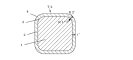
図2は、従来の巻線用絶縁電線の1例(T2)を示す断面図である。図中の符号で、図1と同じものは、図1におけるものと同じ意味である。また、R1’は導体1のコーナー部の曲率半径、R2’は絶縁被覆層2のコーナー部の曲率半径、t’は導体1の平坦部に被覆された絶縁被覆層2の厚さである。図2に示す絶縁電線では、平坦部とコーナー部の絶縁被覆層の厚さが同じであり、コーナー部の形状には、R1’=R2’+t’の関係がある。
FIG. 2 is a cross-sectional view showing an example (T2) of a conventional insulated wire for winding. The same reference numerals in FIG. 1 as those in FIG. 1 have the same meaning as in FIG. R1 'is the radius of curvature of the corner portion of the
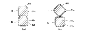
図3は、2本の平角線の巻線用絶縁電線11,12が隣接した状態を断面図により示す説明図であり、(A)は平坦部同士が隣接した場合、(B)はコーナー部と平坦部とが隣接した場合を示す。また、図中、11a、12aは導体、11b、12bは絶縁被覆層を示す。なお、本明細書中では、断面が略四角形の線材を平角線と表記し、断面が略正方形の角線が含まれるものとする。
FIG. 3 is an explanatory view showing a state in which the
図4は、従来の平角線が図3のように隣接した場合に、空隙や絶縁被覆層に作用する電界分布を示したグラフである。図4の縦軸は、2つの平角線の導体間の空隙や絶縁被覆層にかかる電界の大きさ(V/cm)を示し、横軸は、一方の平角線のコーナー部が他方の平角線の平坦部に接する位置(横軸中央が平坦部の中央)を示している。
図4から、コーナー部と平坦部が隣接した場合、平坦部同士が隣接した場合より空隙や絶縁被覆層に作用する電界の最大値が大きくなることがわかる。
FIG. 4 is a graph showing the electric field distribution acting on the air gap and the insulating coating layer when conventional rectangular wires are adjacent as shown in FIG. The vertical axis in FIG. 4 shows the gap between the conductors of two rectangular wires and the magnitude of the electric field applied to the insulating coating layer (V / cm), and the horizontal axis shows the corner of one rectangular wire as the other rectangular wire. The position in contact with the flat portion (the center of the horizontal axis is the center of the flat portion).
FIG. 4 shows that when the corner portion and the flat portion are adjacent to each other, the maximum value of the electric field acting on the air gap and the insulating coating layer is larger than when the flat portions are adjacent to each other.
本発明は、上記実施の形態に限定されることはなく、特許請求の範囲に記載された技術的事項の範囲内において、種々の変更が可能である。例えば、導体と第1の樹脂層(絶縁被覆層)との間に、金属酸化を防止するために金属酸化物又はコーティング層等からなる金属酸化防止層が形成されていてもよい。
また、絶縁被覆層は、1層以上であればよく、絶縁被覆層を2層または3層積層したものであってもよい。この場合、最外層の絶縁被覆層におけるコーナー部が式1を満たしていればよいが、全ての絶縁被覆層におけるコーナー部が式1を満たしていることが最も望ましい。
The present invention is not limited to the above-described embodiments, and various modifications can be made within the scope of the technical matters described in the claims. For example, a metal antioxidant layer made of a metal oxide or a coating layer may be formed between the conductor and the first resin layer (insulating coating layer) in order to prevent metal oxidation.
The insulating coating layer may be one or more layers, and may be a laminate of two or three insulating coating layers. In this case, the corner portion in the outermost insulating coating layer only needs to satisfy
また、絶縁電線の構成としては、導体上に直接、樹脂からなる絶縁被覆層を形成してもよく、図5の断面図に示すように導体1上にまずエナメル絶縁層6を焼き付けた後に、押出成形によって絶縁被覆層5を形成してもよい。
Moreover, as a structure of an insulated wire, you may form the insulation coating layer which consists of resin directly on a conductor, and after baking the
以下、本発明を実施例に基づき、本発明をさらに詳細に説明するが本発明はこれに限定されるものではない。 Hereinafter, the present invention will be described in more detail based on examples, but the present invention is not limited thereto.
実施例1〜2、比較例1、参考例1
無酸素銅からなり、幅2.2mm、コーナーの曲率半径R1が0.3mmの角線の銅線に、ポリフェニレンスルファイド(PPS)からなる絶縁被覆層を押出成形により、表1に示す厚さとコーナー半径R2を有するように被覆し、実施例1〜2および比較例1の絶縁電線を作製した。
実施例1はR2<R1+t/1.5とした場合、実施例2はR2=R1とした場合、比較例1はR2=R1+tとした場合である。これらの絶縁電線のコーナー部と平坦部を隣接させ、下記方法により、空気ギャップの最大電界、絶縁被覆層の最大電界、コロナ放電開始電圧(PDIV)を測定した。また、参考例1として、は実施例1の絶縁電線を平坦部同士を隣接させて、同様に電界およびPDIVを測定した。
表1に、その結果を示す。
Examples 1-2, Comparative Example 1, Reference Example 1
An insulation coating layer made of polyphenylene sulfide (PPS) is extruded on a copper wire made of oxygen-free copper and having a width of 2.2 mm and a corner radius of curvature R1 of 0.3 mm. The insulated wires of Examples 1 and 2 and Comparative Example 1 were manufactured so as to have a corner radius R2.
Example 1 is the case where R2 <R1 + t / 1.5, Example 2 is the case where R2 = R1, and Comparative Example 1 is the case where R2 = R1 + t. The corner portions and flat portions of these insulated wires were made adjacent to each other, and the maximum electric field of the air gap, the maximum electric field of the insulating coating layer, and the corona discharge starting voltage (PDIV) were measured by the following methods. Moreover, as Reference Example 1, the electric field and PDIV were measured in the same manner with the insulated wires of Example 1 having flat portions adjacent to each other.
Table 1 shows the results.
・空気ギャップの最大電界および絶縁被覆の最大電界
実施例1、実施例2および比較例1はコーナー部頂点、参考例1は平坦部において、印加電圧が1kVの電界の最大値を表面電荷法による電界シミュレーションを用いてPPSと空気の比誘電率が各々3.3、1.0の条件により測定した。また、空気ギャップの大きさは1μmである。
・放電開始電圧
部分放電検出器を用いて、常温、常湿の条件下で測定した。
The maximum electric field of the air gap and the maximum electric field of the insulation coating Example 1, Example 2 and Comparative Example 1 are the corner portion apexes, and Reference Example 1 is the flat portion. Using electric field simulation, the relative dielectric constants of PPS and air were measured under the conditions of 3.3 and 1.0, respectively. The size of the air gap is 1 μm.
-Discharge start voltage It measured on the conditions of normal temperature and normal humidity using the partial discharge detector.

表1に示すように、実施例1ではR2=0.38[mm]、実施例2ではR2=0.30[mm]、比較例1ではR2=0.425[mm]を用い、いずれもR1=0.3[mm]、t=0.125[mm]である。
表1から、実施例1では、比較例1に比べ、空気ギャップや絶縁被覆層の最大電界が約10%低減していることがわかる。また、実施例2では、比較例1に比べ、空気ギャップや絶縁被覆層の最大電界が15%以上低減していることがわかる。放電開始電圧も向上している。さらに、実施例2では、参考例1に比べ、絶縁被覆層の最大電界も小さくなっている。
As shown in Table 1, in Example 1, R2 = 0.38 [mm], in Example 2, R2 = 0.30 [mm], and in Comparative Example 1, R2 = 0.425 [mm]. R1 = 0.3 [mm] and t = 0.125 [mm].
From Table 1, it can be seen that in Example 1, the maximum electric field of the air gap and the insulating coating layer is reduced by about 10% compared to Comparative Example 1. Moreover, in Example 2, it turns out that the maximum electric field of an air gap or an insulation coating layer is reducing 15% or more compared with the comparative example 1. The discharge start voltage is also improved. Further, in Example 2, the maximum electric field of the insulating coating layer is smaller than that in Reference Example 1.
実施例3〜4、比較例2、参考例2
絶縁被覆層の厚さtを50μmに薄くした以外は、実施例1〜2、比較例1と同様に、R2<R1+t/1.5とした場合(実施例3)、R2=R1とした場合(実施例4)、R2=R1+tとした場合(比較例3)の絶縁電線を作製した。これらの絶縁電線のコーナー部と平坦部を隣接させ、実施例1と同様に電界を測定した。また、参考例2として実施例3の絶縁電線を平坦部同士を隣接させて同様に電界を測定した。
表2に、その結果を示す。
Examples 3 to 4, Comparative Example 2, Reference Example 2
When R2 <R1 + t / 1.5 (Example 3) and R2 = R1 as in Examples 1 and 2 and Comparative Example 1 except that the thickness t of the insulating coating layer was reduced to 50 μm (Embodiment 4) An insulated wire was prepared when R2 = R1 + t (Comparative Example 3). The electric field was measured in the same manner as in Example 1 with the corner portions and flat portions of these insulated wires adjacent to each other. Further, as Reference Example 2, the electric field of the insulated wire of Example 3 was measured in the same manner with flat portions adjacent to each other.
Table 2 shows the results.
表2からわかるように、絶縁被覆層の厚さを薄くしても、実施例1〜2と同様に電界を低減する効果を奏する。 As can be seen from Table 2, even if the thickness of the insulating coating layer is reduced, the effect of reducing the electric field is obtained as in Examples 1-2.
実施例5〜6、比較例3、参考例3
導体コーナーR1を0.2mmに小さくした以外は、実施例1〜2、比較例1と同様に、R2<R1+t/1.5とした場合(実施例5)、R2=R1とした場合(実施例6)、R2=R1+tとした場合(比較例3)の絶縁電線を作製した。これらの絶縁電線のコーナー部と平坦部を隣接させ、実施例1と同様に電界を測定した。また、参考例3として実施例5の絶縁電線を平坦部同士を隣接させて同様に電界を測定した。
表3に、その結果を示す。
Examples 5 to 6, Comparative Example 3, Reference Example 3
Except for reducing the conductor corner R1 to 0.2 mm, as in Examples 1-2 and Comparative Example 1, when R2 <R1 + t / 1.5 (Example 5), when R2 = R1 (Implementation) Example 6) An insulated wire was produced when R2 = R1 + t (Comparative Example 3). The electric field was measured in the same manner as in Example 1 with the corner portions and flat portions of these insulated wires adjacent to each other. Further, as Reference Example 3, the electric field of the insulated wire of Example 5 was measured in the same manner with flat portions adjacent to each other.
Table 3 shows the results.
以上のことから、R2<R1+t/1.5の関係にあると、コーナー部の電界集中を抑制でき、PDIVの向上を図ることができる。さらにR2≦R1の関係にあると、絶縁被覆層の電界を小さくできるためBDVの向上ができる。 From the above, when the relationship of R2 <R1 + t / 1.5 is satisfied, the electric field concentration at the corner can be suppressed and the PDIV can be improved. Further, when the relation of R2 ≦ R1 is established, the electric field of the insulating coating layer can be reduced, so that BDV can be improved.
T1,T2 巻線用絶縁電線
1 導体
2 絶縁被覆層
3 導体コーナー部
4 絶縁被覆層コーナー部
5 絶縁被覆層
6 エナメル絶縁層
11,12 巻線用絶縁電線
11a、12a 導体
11b、12b 絶縁被覆層
T1, T2 Winding insulated
Claims (6)
前記導体の平坦部に被覆された前記絶縁被覆層の厚さt[mm]、前記導体のコーナー部の曲率半径R1[mm]、および前記絶縁被覆層のコーナー部の曲率半径R2[mm]が下記関係式、
0<R2<R1+t/1.5
を満たすことを特徴とする巻線用絶縁電線。 An insulated wire for winding having at least one insulating coating layer made of resin on the outer periphery of a conductor having a substantially rectangular cross section,
The thickness t [mm] of the insulating coating layer coated on the flat portion of the conductor, the radius of curvature R1 [mm] of the corner portion of the conductor, and the radius of curvature R2 [mm] of the corner portion of the insulating coating layer. The following relational expression,
0 <R2 <R1 + t / 1.5
An insulated wire for winding, characterized by satisfying
前記導体の平坦部の絶縁被覆層の厚さt[mm]、前記導体のコーナー部の曲率半径R1[mm]、および絶縁被覆層のコーナー部の曲率半径R2[mm]が下記関係式、
0<R2<R1+t/1.5
を満たすように前記絶縁被覆層を押出成形することを特徴とする巻線用絶縁電線の製造方法。 A method for producing an insulated wire for winding having at least one insulating coating layer made of a resin on the outer periphery of a conductor having a substantially rectangular cross section,
The thickness t [mm] of the insulating coating layer of the flat portion of the conductor, the curvature radius R1 [mm] of the corner portion of the conductor, and the curvature radius R2 [mm] of the corner portion of the insulating coating layer are expressed by the following relational expressions:
0 <R2 <R1 + t / 1.5
A method of manufacturing an insulated wire for winding, wherein the insulating coating layer is extruded so as to satisfy.
前記導体の平坦部の絶縁被覆層の厚さt[mm]、前記導体のコーナー部の曲率半径R1[mm]、および絶縁被覆層のコーナー部の曲率半径R2[mm]が下記関係式、
0<R2<R1+t/1.5
を満たすように前記絶縁被覆層を押出成形して巻線用絶縁電線を製造する工程と
前記巻線用絶縁電線を巻線に加工する工程と
を備えることを特徴とする、コイルの製造方法。 A coil manufacturing method using an insulated wire for winding having at least one insulating coating layer made of resin on the outer periphery of a conductor having a substantially rectangular cross section,
The thickness t [mm] of the insulating coating layer of the flat portion of the conductor, the curvature radius R1 [mm] of the corner portion of the conductor, and the curvature radius R2 [mm] of the corner portion of the insulating coating layer are expressed by the following relational expressions:
0 <R2 <R1 + t / 1.5
A method for manufacturing a coil, comprising: a step of manufacturing the insulated wire for winding by extruding the insulating coating layer so as to satisfy the condition; and a step of processing the insulated wire for winding into a winding.
Priority Applications (1)
| Application Number | Priority Date | Filing Date | Title |
|---|---|---|---|
| JP2008220514A JP5137749B2 (en) | 2008-08-28 | 2008-08-28 | Insulated wire for winding and method of manufacturing coil |
Applications Claiming Priority (1)
| Application Number | Priority Date | Filing Date | Title |
|---|---|---|---|
| JP2008220514A JP5137749B2 (en) | 2008-08-28 | 2008-08-28 | Insulated wire for winding and method of manufacturing coil |
Publications (2)
| Publication Number | Publication Date |
|---|---|
| JP2010055965A true JP2010055965A (en) | 2010-03-11 |
| JP5137749B2 JP5137749B2 (en) | 2013-02-06 |
Family
ID=42071652
Family Applications (1)
| Application Number | Title | Priority Date | Filing Date |
|---|---|---|---|
| JP2008220514A Active JP5137749B2 (en) | 2008-08-28 | 2008-08-28 | Insulated wire for winding and method of manufacturing coil |
Country Status (1)
| Country | Link |
|---|---|
| JP (1) | JP5137749B2 (en) |
Cited By (13)
| Publication number | Priority date | Publication date | Assignee | Title |
|---|---|---|---|---|
| KR20110109084A (en) * | 2010-03-30 | 2011-10-06 | 엘에스전선 주식회사 | Rectangular enamel wire and manufacturing method thereof |
| JP2011223768A (en) * | 2010-04-12 | 2011-11-04 | Toyota Motor Corp | Arrangement method of temperature detecting element, and motor |
| WO2013073384A1 (en) * | 2011-11-14 | 2013-05-23 | 住友電気工業株式会社 | Reactor, molded coil, converter, and power conversion device |
| JP2013171657A (en) * | 2012-02-20 | 2013-09-02 | Furukawa Electric Co Ltd:The | Marking method of covered electric wire, marking device, and manufacturing apparatus of covered electric wire |
| WO2014049870A1 (en) * | 2012-09-28 | 2014-04-03 | 富士機械製造株式会社 | Coil for high frequency power and method for manufacturing same |
| JP2017059323A (en) * | 2015-09-14 | 2017-03-23 | ダイキン工業株式会社 | Insulated wire and method of manufacturing the same |
| EP3217410A4 (en) * | 2016-03-08 | 2018-04-04 | LS Cable & System Ltd. | Corona-resistant flat wire |
| JP2018082091A (en) * | 2016-11-17 | 2018-05-24 | Tdk株式会社 | Coil device |
| JP2018143072A (en) * | 2017-02-28 | 2018-09-13 | 株式会社小松製作所 | Flat wire for wave-winding coil |
| JP2019029454A (en) * | 2017-07-27 | 2019-02-21 | 富士電機株式会社 | Core and transformer |
| WO2019087466A1 (en) * | 2017-11-01 | 2019-05-09 | 三菱電機株式会社 | Transformer and power conversion device |
| WO2022250059A1 (en) * | 2021-05-26 | 2022-12-01 | 古河電気工業株式会社 | Superconducting rectangular wire material for superconducting coil, and superconducting coil |
| WO2023139995A1 (en) * | 2022-01-21 | 2023-07-27 | 株式会社オートネットワーク技術研究所 | Stator |
Families Citing this family (1)
| Publication number | Priority date | Publication date | Assignee | Title |
|---|---|---|---|---|
| CN106104707B (en) | 2013-12-26 | 2019-05-10 | 古河电气工业株式会社 | The manufacturing method of insulated electric conductor, motor coil, electric/electronic and insulated electric conductor |
Citations (4)
| Publication number | Priority date | Publication date | Assignee | Title |
|---|---|---|---|---|
| JPH03152808A (en) * | 1989-11-09 | 1991-06-28 | Furukawa Electric Co Ltd:The | Transposed rectangular conductor insulated wire |
| JP2005203334A (en) * | 2003-12-17 | 2005-07-28 | Furukawa Electric Co Ltd:The | Insulated wire and its manufacturing method |
| JP2005209378A (en) * | 2004-01-20 | 2005-08-04 | Mitsubishi Cable Ind Ltd | Manufacturing method of flat insulated wire |
| JP2009123418A (en) * | 2007-11-13 | 2009-06-04 | Nippon Soken Inc | Flat rectangular electric wire |
-
2008
- 2008-08-28 JP JP2008220514A patent/JP5137749B2/en active Active
Patent Citations (4)
| Publication number | Priority date | Publication date | Assignee | Title |
|---|---|---|---|---|
| JPH03152808A (en) * | 1989-11-09 | 1991-06-28 | Furukawa Electric Co Ltd:The | Transposed rectangular conductor insulated wire |
| JP2005203334A (en) * | 2003-12-17 | 2005-07-28 | Furukawa Electric Co Ltd:The | Insulated wire and its manufacturing method |
| JP2005209378A (en) * | 2004-01-20 | 2005-08-04 | Mitsubishi Cable Ind Ltd | Manufacturing method of flat insulated wire |
| JP2009123418A (en) * | 2007-11-13 | 2009-06-04 | Nippon Soken Inc | Flat rectangular electric wire |
Cited By (19)
| Publication number | Priority date | Publication date | Assignee | Title |
|---|---|---|---|---|
| KR20110109084A (en) * | 2010-03-30 | 2011-10-06 | 엘에스전선 주식회사 | Rectangular enamel wire and manufacturing method thereof |
| KR101711648B1 (en) * | 2010-03-30 | 2017-03-03 | 엘에스전선 주식회사 | Rectangular enamel wire and manufacturing method thereof |
| JP2011223768A (en) * | 2010-04-12 | 2011-11-04 | Toyota Motor Corp | Arrangement method of temperature detecting element, and motor |
| WO2013073384A1 (en) * | 2011-11-14 | 2013-05-23 | 住友電気工業株式会社 | Reactor, molded coil, converter, and power conversion device |
| JP2013128099A (en) * | 2011-11-14 | 2013-06-27 | Sumitomo Electric Ind Ltd | Reactor, molded coil, converter, and power conversion device |
| US9460842B2 (en) | 2011-11-14 | 2016-10-04 | Sumitomo Electric Industries, Ltd. | Reactor, coil mold product, converter, and power converter apparatus |
| JP2013171657A (en) * | 2012-02-20 | 2013-09-02 | Furukawa Electric Co Ltd:The | Marking method of covered electric wire, marking device, and manufacturing apparatus of covered electric wire |
| WO2014049870A1 (en) * | 2012-09-28 | 2014-04-03 | 富士機械製造株式会社 | Coil for high frequency power and method for manufacturing same |
| JP2017059323A (en) * | 2015-09-14 | 2017-03-23 | ダイキン工業株式会社 | Insulated wire and method of manufacturing the same |
| EP3217410A4 (en) * | 2016-03-08 | 2018-04-04 | LS Cable & System Ltd. | Corona-resistant flat wire |
| JP2018082091A (en) * | 2016-11-17 | 2018-05-24 | Tdk株式会社 | Coil device |
| JP2018143072A (en) * | 2017-02-28 | 2018-09-13 | 株式会社小松製作所 | Flat wire for wave-winding coil |
| JP2019029454A (en) * | 2017-07-27 | 2019-02-21 | 富士電機株式会社 | Core and transformer |
| WO2019087466A1 (en) * | 2017-11-01 | 2019-05-09 | 三菱電機株式会社 | Transformer and power conversion device |
| JPWO2019087466A1 (en) * | 2017-11-01 | 2019-11-14 | 三菱電機株式会社 | Power converter |
| EP3706150A4 (en) * | 2017-11-01 | 2021-02-17 | Mitsubishi Electric Corporation | Transformer and power conversion device |
| US11290019B2 (en) | 2017-11-01 | 2022-03-29 | Mitsubishi Electric Corporation | Power converter |
| WO2022250059A1 (en) * | 2021-05-26 | 2022-12-01 | 古河電気工業株式会社 | Superconducting rectangular wire material for superconducting coil, and superconducting coil |
| WO2023139995A1 (en) * | 2022-01-21 | 2023-07-27 | 株式会社オートネットワーク技術研究所 | Stator |
Also Published As
| Publication number | Publication date |
|---|---|
| JP5137749B2 (en) | 2013-02-06 |
Similar Documents
| Publication | Publication Date | Title |
|---|---|---|
| JP5137749B2 (en) | Insulated wire for winding and method of manufacturing coil | |
| JP5019594B2 (en) | Insulated wire | |
| KR102000380B1 (en) | Insulated electrical wire having excellent resistance to bending process, coil and electronic/electric equipment using same | |
| JP5391341B1 (en) | Inverter surge resistant wire | |
| US11217364B2 (en) | Insulated wire, coil, and electric/electronic equipments | |
| WO2017175516A1 (en) | Insulated wire, coil, and electric/electronic apparatus | |
| KR20160133518A (en) | Insulation wire, insulation wire manufacturing method, method of manufacturing stator for rotary electric machine and rotary electric machine | |
| CN108604483B (en) | Insulated wire, motor coil, and electric/electronic device | |
| KR102106918B1 (en) | Winding, coil and transformer | |
| CN103985438A (en) | Electrical cable resistant to partial discharges | |
| JP5304608B2 (en) | Electric wire manufacturing method | |
| JP2020191271A (en) | Insulated wire, coil and electric/electronic apparatus | |
| JP2009245652A (en) | Insulated wire | |
| JP7050566B2 (en) | High frequency high output transformer | |
| JP6519231B2 (en) | Winding and method of manufacturing the same | |
| JP6858799B2 (en) | Manufacturing methods for insulated wires, coils, electrical and electronic equipment, and insulated wires | |
| WO2023153246A1 (en) | Insulated wire, coil, rotating electric machine, and electric/electronic device | |
| JP7306789B2 (en) | coil and transformer | |
| WO2024038680A1 (en) | Insulated electric wire, manufacturing method therefor, and coil, rotary electric machine, and electrical and electronic equipment using said insulated electric wire | |
| JP7257558B1 (en) | Insulated wires, coils, rotating electrical machines, and electric/electronic equipment | |
| JP2023143124A (en) | Flat cable, coil, and production method of flat cable | |
| JP7216555B2 (en) | Insulated wire with high heat dissipation and coil using the same | |
| JP2021118338A (en) | Spacer for electric wire, composite material for electric wire, electric wire, coil, transformer and power conversion circuit device | |
| JP2021190403A (en) | coaxial cable | |
| JP2023135383A (en) | Twisted wire, insulated wire, coil and transformer |
Legal Events
| Date | Code | Title | Description |
|---|---|---|---|
| A977 | Report on retrieval |
Free format text: JAPANESE INTERMEDIATE CODE: A971007 Effective date: 20120720 |
|
| A131 | Notification of reasons for refusal |
Free format text: JAPANESE INTERMEDIATE CODE: A131 Effective date: 20120731 |
|
| A521 | Request for written amendment filed |
Free format text: JAPANESE INTERMEDIATE CODE: A523 Effective date: 20120928 |
|
| TRDD | Decision of grant or rejection written | ||
| A01 | Written decision to grant a patent or to grant a registration (utility model) |
Free format text: JAPANESE INTERMEDIATE CODE: A01 Effective date: 20121030 |
|
| A01 | Written decision to grant a patent or to grant a registration (utility model) |
Free format text: JAPANESE INTERMEDIATE CODE: A01 |
|
| A61 | First payment of annual fees (during grant procedure) |
Free format text: JAPANESE INTERMEDIATE CODE: A61 Effective date: 20121113 |
|
| R151 | Written notification of patent or utility model registration |
Ref document number: 5137749 Country of ref document: JP Free format text: JAPANESE INTERMEDIATE CODE: R151 |
|
| FPAY | Renewal fee payment (event date is renewal date of database) |
Free format text: PAYMENT UNTIL: 20151122 Year of fee payment: 3 |
|
| R250 | Receipt of annual fees |
Free format text: JAPANESE INTERMEDIATE CODE: R250 |
|
| S111 | Request for change of ownership or part of ownership |
Free format text: JAPANESE INTERMEDIATE CODE: R313111 |
|
| R350 | Written notification of registration of transfer |
Free format text: JAPANESE INTERMEDIATE CODE: R350 |
|
| R250 | Receipt of annual fees |
Free format text: JAPANESE INTERMEDIATE CODE: R250 |
|
| R250 | Receipt of annual fees |
Free format text: JAPANESE INTERMEDIATE CODE: R250 |
|
| R250 | Receipt of annual fees |
Free format text: JAPANESE INTERMEDIATE CODE: R250 |