JP2010055697A - 半導体記憶装置及びそのテスト方法 - Google Patents
半導体記憶装置及びそのテスト方法 Download PDFInfo
- Publication number
- JP2010055697A JP2010055697A JP2008220570A JP2008220570A JP2010055697A JP 2010055697 A JP2010055697 A JP 2010055697A JP 2008220570 A JP2008220570 A JP 2008220570A JP 2008220570 A JP2008220570 A JP 2008220570A JP 2010055697 A JP2010055697 A JP 2010055697A
- Authority
- JP
- Japan
- Prior art keywords
- sense amplifier
- bit line
- memory device
- semiconductor memory
- circuit
- Prior art date
- Legal status (The legal status is an assumption and is not a legal conclusion. Google has not performed a legal analysis and makes no representation as to the accuracy of the status listed.)
- Granted
Links
- 239000004065 semiconductor Substances 0.000 title claims abstract description 30
- 238000010998 test method Methods 0.000 title claims abstract description 8
- 238000012360 testing method Methods 0.000 claims abstract description 41
- 230000003321 amplification Effects 0.000 claims abstract description 7
- 238000003199 nucleic acid amplification method Methods 0.000 claims abstract description 7
- 238000000034 method Methods 0.000 claims description 2
- 238000010586 diagram Methods 0.000 description 8
- 238000003491 array Methods 0.000 description 6
- 230000003071 parasitic effect Effects 0.000 description 6
- 102100020800 DNA damage-regulated autophagy modulator protein 1 Human genes 0.000 description 4
- 101000931929 Homo sapiens DNA damage-regulated autophagy modulator protein 1 Proteins 0.000 description 4
- 239000003990 capacitor Substances 0.000 description 4
- 238000004519 manufacturing process Methods 0.000 description 4
- 230000002093 peripheral effect Effects 0.000 description 4
- 230000007423 decrease Effects 0.000 description 2
- 238000005259 measurement Methods 0.000 description 2
- 230000002950 deficient Effects 0.000 description 1
- 238000012986 modification Methods 0.000 description 1
- 230000004048 modification Effects 0.000 description 1
- 230000004044 response Effects 0.000 description 1
Images


Classifications
-
- G—PHYSICS
- G11—INFORMATION STORAGE
- G11C—STATIC STORES
- G11C29/00—Checking stores for correct operation ; Subsequent repair; Testing stores during standby or offline operation
- G11C29/02—Detection or location of defective auxiliary circuits, e.g. defective refresh counters
-
- G—PHYSICS
- G11—INFORMATION STORAGE
- G11C—STATIC STORES
- G11C29/00—Checking stores for correct operation ; Subsequent repair; Testing stores during standby or offline operation
- G11C29/02—Detection or location of defective auxiliary circuits, e.g. defective refresh counters
- G11C29/026—Detection or location of defective auxiliary circuits, e.g. defective refresh counters in sense amplifiers
-
- G—PHYSICS
- G11—INFORMATION STORAGE
- G11C—STATIC STORES
- G11C11/00—Digital stores characterised by the use of particular electric or magnetic storage elements; Storage elements therefor
- G11C11/21—Digital stores characterised by the use of particular electric or magnetic storage elements; Storage elements therefor using electric elements
- G11C11/34—Digital stores characterised by the use of particular electric or magnetic storage elements; Storage elements therefor using electric elements using semiconductor devices
- G11C11/40—Digital stores characterised by the use of particular electric or magnetic storage elements; Storage elements therefor using electric elements using semiconductor devices using transistors
- G11C11/401—Digital stores characterised by the use of particular electric or magnetic storage elements; Storage elements therefor using electric elements using semiconductor devices using transistors forming cells needing refreshing or charge regeneration, i.e. dynamic cells
- G11C11/4063—Auxiliary circuits, e.g. for addressing, decoding, driving, writing, sensing or timing
- G11C11/407—Auxiliary circuits, e.g. for addressing, decoding, driving, writing, sensing or timing for memory cells of the field-effect type
- G11C11/409—Read-write [R-W] circuits
- G11C11/4091—Sense or sense/refresh amplifiers, or associated sense circuitry, e.g. for coupled bit-line precharging, equalising or isolating
-
- G—PHYSICS
- G11—INFORMATION STORAGE
- G11C—STATIC STORES
- G11C11/00—Digital stores characterised by the use of particular electric or magnetic storage elements; Storage elements therefor
- G11C11/21—Digital stores characterised by the use of particular electric or magnetic storage elements; Storage elements therefor using electric elements
- G11C11/34—Digital stores characterised by the use of particular electric or magnetic storage elements; Storage elements therefor using electric elements using semiconductor devices
- G11C11/40—Digital stores characterised by the use of particular electric or magnetic storage elements; Storage elements therefor using electric elements using semiconductor devices using transistors
- G11C11/401—Digital stores characterised by the use of particular electric or magnetic storage elements; Storage elements therefor using electric elements using semiconductor devices using transistors forming cells needing refreshing or charge regeneration, i.e. dynamic cells
- G11C11/4063—Auxiliary circuits, e.g. for addressing, decoding, driving, writing, sensing or timing
- G11C11/407—Auxiliary circuits, e.g. for addressing, decoding, driving, writing, sensing or timing for memory cells of the field-effect type
- G11C11/409—Read-write [R-W] circuits
- G11C11/4097—Bit-line organisation, e.g. bit-line layout, folded bit lines
-
- G—PHYSICS
- G11—INFORMATION STORAGE
- G11C—STATIC STORES
- G11C29/00—Checking stores for correct operation ; Subsequent repair; Testing stores during standby or offline operation
- G11C29/04—Detection or location of defective memory elements, e.g. cell constructio details, timing of test signals
- G11C29/08—Functional testing, e.g. testing during refresh, power-on self testing [POST] or distributed testing
- G11C29/12—Built-in arrangements for testing, e.g. built-in self testing [BIST] or interconnection details
- G11C2029/1204—Bit line control
-
- G—PHYSICS
- G11—INFORMATION STORAGE
- G11C—STATIC STORES
- G11C29/00—Checking stores for correct operation ; Subsequent repair; Testing stores during standby or offline operation
- G11C29/04—Detection or location of defective memory elements, e.g. cell constructio details, timing of test signals
- G11C29/50—Marginal testing, e.g. race, voltage or current testing
- G11C2029/5006—Current
Landscapes
- For Increasing The Reliability Of Semiconductor Memories (AREA)
- Dram (AREA)
Abstract
【解決手段】本発明の半導体記憶装置は、選択されたメモリセルMCから読み出された信号を伝送する第1のビット線LBLと、第1のビット線LBLの信号電圧を増幅して出力電流に変換する増幅素子Q1を含むシングルエンド型の第1のセンスアンプ回路21と、第1のセンスアンプ回路を流れる電流(独立の接地電位VSSLを経由する電流)を、他の回路部分を流れる電流とは独立に測定するテスト動作を制御する制御回路とを備えている。
【選択図】図2
Description
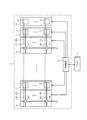
図1は、第1実施形態のDRAM1の全体構成を示している。図1においては、複数のメモリセルアレイ10と、複数のローカルセンスアンプ列11と、1つのグローバルセンスアンプ列12と、制御回路13とを含んで構成されるDRAM1と、DRAM1に対するテストを実行するテスタ2が示されている。

Wg:実効ゲート幅
Lg:実効ゲート長
Vt:しきい値
Vgs:ゲートソース間電圧
次に、第2実施形態のDRAM1について説明する。第2実施形態のDRAM1の全体構成については、第1実施形態の図1と共通であるので、説明を省略する。図9は、第2実施形態のローカルセンスアンプ21とその周辺部の具体的な構成を示している。図9における回路構成は、ほぼ第1実施形態と共通しているが、ローカルセンスアンプ21のNMOSトランジスタQ2(本発明の第2のプリチャージ回路)のソースが制御電圧VPLCに接続されている点が変更されている。なお、他の点については図2と同様であり、グローバルセンスアンプ22の回路構成についても図3と同様であるため、説明を省略する。
2…テスタ
10…メモリセルアレイ
11…ローカルセンスアンプ列
12…グローバルセンスアンプ列
13…制御回路
21…ローカルセンスアンプ
22…グローバルセンスアンプ
22a…信号電圧判定ラッチ
30〜33…ラッチ回路
D、D’…ディレイ素子
MC…メモリセル
WL…ワード線
GBL…グローバルビット線
LBL…ローカルビット線
Q0、Q1〜Q5、Q11、Q12、Q14、Q16〜Q20…NMOSトランジスタ
Q10、Q13、Q15…PMOSトランジスタ
VSSL…接地電位
VDD、VARY…電源電圧
VPLT…セルプレート電位
PC、PCG…プリチャージ信号
RT、WT、LTC、RES、WE、R1ACT、R2ACT…制御信号
YS…選択信号
SD…出力信号
RBUS…読み出し信号線
WBUS…書き込み信号線
Claims (13)
- 複数のメモリセルを含むメモリセルアレイを備える半導体記憶装置であって、
前記メモリセルアレイのうちの選択されたメモリセルから読み出された信号を伝送する第1のビット線と、
前記第1のビット線の信号電圧を増幅して出力電流に変換する増幅素子を含むシングルエンド型の第1のセンスアンプ回路と、
前記第1のセンスアンプ回路を流れる電流を、他の回路部分を流れる電流とは独立に測定するテスト動作を制御する制御回路と、
を備えることを特徴とする半導体記憶装置。 - 複数の前記第1のビット線と、複数の前記第1のセンスアンプ回路とが設けられ、前記制御回路は、複数の前記第1のセンスアンプ回路を流れる総電流を測定する前記テスト動作を制御することを特徴とする請求項1に記載の半導体記憶装置。
- 前記複数の第1のセンスアンプ回路は、他の回路部分に接続される接地電位とは独立した第1の接地電位に接続され、当該第1の接地電位が端子を介して外部と接続可能に構成されていることを特徴とする請求項2に記載の半導体記憶装置。
- 前記増幅素子は、ゲートが前記第1のビット線に接続され、ソースが前記第1の接地電位に接続されたNMOSトランジスタであり、前記出力電流として前記第1のビット線の電位に応じたドレイン電流が流れることを特徴とする請求項3に記載の半導体記憶装置。
- 各々の前記第1のセンスアンプ回路は、前記第1のビット線を前記第1の接地電位にプリチャージする第1のプリチャージ回路を含むことを特徴とする請求項3に記載の半導体記憶装置。
- 各々の前記第1のセンスアンプ回路は、前記第1のビット線を所定の制御電圧にプリチャージする第2のプリチャージ回路を含み、
前記制御回路は、前記第1のビット線が前記所定の制御電圧にプリチャージされた状態で前記テスト動作を制御することを特徴とする請求項1に記載の半導体記憶装置。 - 前記第1のセンスアンプ回路を介して前記第1のビット線と選択的に接続される第2のビット線をさらに備えることを特徴とする請求項1に記載の半導体記憶装置。
- 前記出力電流を供給された状態の前記第2のビット線の信号電圧のレベルを判定する第2のセンスアンプ回路をさらに備えることを特徴とする請求項7に記載の半導体記憶装置。
- 前記制御回路に入力されるテスト信号が活性化されたとき、前記第2のビット線を所定電位の電源にプリチャージする第3のプリチャージ回路を含むことを特徴とする請求項7に記載の半導体記憶装置。
- 前記制御回路に入力されるテスト信号が活性化されたとき、前記第2のビット線を前記増幅素子に接続して前記出力電流が流れる状態にするスイッチ回路を含むことを特徴とする請求項9に記載の半導体記憶装置。
- 複数のメモリセルを階層化して配置したメモリセルアレイが構成され、
前記第1のビット線としての所定数のローカルビット線が、前記第2のビット線としてのグローバルビット線の区分に対応して配置され、
各々の前記ローカルビット線に接続される前記第1のセンスアンプ回路としての複数のローカルセンスアンプと、各々の前記グローバルビット線に接続される前記第2のセンスアンプ回路としてのグローバルセンスアンプとが設けられていることを特徴とする請求項8に記載の半導体記憶装置。 - 複数のメモリセルを含むメモリセルアレイのうちの選択されたメモリセルから読み出された信号を伝送する複数の第1のビット線と、前記第1のビット線の信号電圧を増幅して出力電流に変換する増幅素子を含むシングルエンド型の複数の第1のセンスアンプ回路と、前記複数の第1のセンスアンプ回路を流れる電流を、他の回路部分を流れる電流とは独立に測定するテスト動作を制御する制御回路とを備える半導体記憶装置のテスト方法であって、
N(Nは2以上の整数)個の前記メモリセルから読み出した各信号をN本の前記第1のビット線に伝送させ、当該N本の第1のビット線の各信号電圧をN個の前記第1のセンスアンプ回路により増幅し、当該N個全ての第1のセンスアンプ回路を流れる総電流を測定し、測定された総電流値に基づいて前記増幅素子のしきい値電圧の平均値を算出する、ことを特徴とする半導体記憶装置のテスト方法。 - 請求項6に記載の半導体記憶装置のテスト方法であって、
N本の前記第1のビット線をそれぞれ前記第2のプリチャージ回路により前記所定の制御電圧にプリチャージし、当該N本の第1のビット線の各信号電圧をN個の前記第1のセンスアンプ回路により増幅し、当該N個全ての前記第1のセンスアンプ回路を流れる総電流を測定し、測定された総電流値に基づいて前記増幅素子のしきい値電圧の平均値を算出する、ことを特徴とする半導体記憶装置のテスト方法。
Priority Applications (2)
| Application Number | Priority Date | Filing Date | Title |
|---|---|---|---|
| JP2008220570A JP5433187B2 (ja) | 2008-08-28 | 2008-08-28 | 半導体記憶装置及びそのテスト方法 |
| US12/549,184 US8189413B2 (en) | 2008-08-28 | 2009-08-27 | Semiconductor memory device, test method thereof and semiconductor device |
Applications Claiming Priority (1)
| Application Number | Priority Date | Filing Date | Title |
|---|---|---|---|
| JP2008220570A JP5433187B2 (ja) | 2008-08-28 | 2008-08-28 | 半導体記憶装置及びそのテスト方法 |
Publications (2)
| Publication Number | Publication Date |
|---|---|
| JP2010055697A true JP2010055697A (ja) | 2010-03-11 |
| JP5433187B2 JP5433187B2 (ja) | 2014-03-05 |
Family
ID=41725273
Family Applications (1)
| Application Number | Title | Priority Date | Filing Date |
|---|---|---|---|
| JP2008220570A Expired - Fee Related JP5433187B2 (ja) | 2008-08-28 | 2008-08-28 | 半導体記憶装置及びそのテスト方法 |
Country Status (2)
| Country | Link |
|---|---|
| US (1) | US8189413B2 (ja) |
| JP (1) | JP5433187B2 (ja) |
Cited By (1)
| Publication number | Priority date | Publication date | Assignee | Title |
|---|---|---|---|---|
| JP2013065638A (ja) * | 2011-09-15 | 2013-04-11 | Elpida Memory Inc | 半導体装置 |
Families Citing this family (4)
| Publication number | Priority date | Publication date | Assignee | Title |
|---|---|---|---|---|
| TWI399754B (zh) * | 2008-03-17 | 2013-06-21 | Elpida Memory Inc | 具有單端感測放大器之半導體裝置 |
| JP5451281B2 (ja) | 2009-09-16 | 2014-03-26 | ピーエスフォー ルクスコ エスエイアールエル | センスアンプ回路及びそれを備えた半導体装置 |
| JP2011159365A (ja) * | 2010-02-02 | 2011-08-18 | Elpida Memory Inc | 半導体装置及び半導体装置を含む情報処理システム |
| CN104464824B (zh) * | 2013-09-17 | 2017-12-01 | 中芯国际集成电路制造(北京)有限公司 | 存储阵列中的mos管阈值电压的测试方法 |
Citations (4)
| Publication number | Priority date | Publication date | Assignee | Title |
|---|---|---|---|---|
| JP2001091599A (ja) * | 1999-09-28 | 2001-04-06 | Nec Ic Microcomput Syst Ltd | 半導体集積回路 |
| WO2007004289A1 (ja) * | 2005-07-04 | 2007-01-11 | National University Corporation Tohoku University | テスト用回路、ウェハ、測定装置、デバイス製造方法、及び表示装置 |
| JP2008171920A (ja) * | 2007-01-10 | 2008-07-24 | Toppan Printing Co Ltd | 半導体評価回路及び評価方法 |
| JP2009266364A (ja) * | 2008-04-04 | 2009-11-12 | Elpida Memory Inc | 半導体記憶装置 |
Family Cites Families (8)
| Publication number | Priority date | Publication date | Assignee | Title |
|---|---|---|---|---|
| JP3529534B2 (ja) | 1996-03-04 | 2004-05-24 | 富士通株式会社 | 半導体記憶装置 |
| JP3521979B2 (ja) * | 1994-11-28 | 2004-04-26 | 富士通株式会社 | 半導体記憶装置 |
| US5701269A (en) * | 1994-11-28 | 1997-12-23 | Fujitsu Limited | Semiconductor memory with hierarchical bit lines |
| WO1996031882A1 (en) | 1995-04-05 | 1996-10-10 | Micron Technology, Inc. | Memory circuit with hierarchical bit line structure |
| JP2000057761A (ja) | 1998-06-03 | 2000-02-25 | Matsushita Electric Ind Co Ltd | 半導体記憶装置 |
| US6999370B2 (en) * | 2003-08-06 | 2006-02-14 | International Business Machines Corporation | Low power circuits with small voltage swing transmission, voltage regeneration, and wide bandwidth architecture |
| KR100583112B1 (ko) * | 2003-11-27 | 2006-05-23 | 주식회사 하이닉스반도체 | 싱글엔디드 센싱 구조를 갖는 불휘발성 강유전체 메모리장치 |
| US7286385B2 (en) * | 2005-07-27 | 2007-10-23 | International Business Machines Corporation | Differential and hierarchical sensing for memory circuits |
-
2008
- 2008-08-28 JP JP2008220570A patent/JP5433187B2/ja not_active Expired - Fee Related
-
2009
- 2009-08-27 US US12/549,184 patent/US8189413B2/en not_active Expired - Fee Related
Patent Citations (4)
| Publication number | Priority date | Publication date | Assignee | Title |
|---|---|---|---|---|
| JP2001091599A (ja) * | 1999-09-28 | 2001-04-06 | Nec Ic Microcomput Syst Ltd | 半導体集積回路 |
| WO2007004289A1 (ja) * | 2005-07-04 | 2007-01-11 | National University Corporation Tohoku University | テスト用回路、ウェハ、測定装置、デバイス製造方法、及び表示装置 |
| JP2008171920A (ja) * | 2007-01-10 | 2008-07-24 | Toppan Printing Co Ltd | 半導体評価回路及び評価方法 |
| JP2009266364A (ja) * | 2008-04-04 | 2009-11-12 | Elpida Memory Inc | 半導体記憶装置 |
Cited By (2)
| Publication number | Priority date | Publication date | Assignee | Title |
|---|---|---|---|---|
| JP2013065638A (ja) * | 2011-09-15 | 2013-04-11 | Elpida Memory Inc | 半導体装置 |
| US9514792B2 (en) | 2011-09-15 | 2016-12-06 | Longitude Semiconductor S.A.R.L. | Semiconductor device having stacked layers |
Also Published As
| Publication number | Publication date |
|---|---|
| US20100054063A1 (en) | 2010-03-04 |
| US8189413B2 (en) | 2012-05-29 |
| JP5433187B2 (ja) | 2014-03-05 |
Similar Documents
| Publication | Publication Date | Title |
|---|---|---|
| US8964478B2 (en) | Semiconductor device | |
| US7663942B2 (en) | Semiconductor memory device having local and global bit lines | |
| US20050190588A1 (en) | Semiconductor device | |
| US7590003B2 (en) | Self-reference sense amplifier circuit and sensing method | |
| US7447088B2 (en) | Semiconductor memory device having an open bit line structure, and method of testing the same | |
| JP2011129237A (ja) | 半導体装置及び半導体記憶装置 | |
| US10236036B2 (en) | Sense amplifier signal boost | |
| JP3745877B2 (ja) | 半導体メモリ装置のメモリセルテスト用の高電圧感知回路 | |
| US6449208B1 (en) | Semiconductor memory device capable of switching reference voltage for generating intermediate voltage | |
| JP5106760B2 (ja) | プリチャージ及び感知増幅スキームを改善した集積回路メモリ装置のビットライン駆動回路及び駆動方法 | |
| JP5433187B2 (ja) | 半導体記憶装置及びそのテスト方法 | |
| KR100824798B1 (ko) | 에지 서브 어레이에 전체 데이터 패턴을 기입할 수 있는 오픈 비트 라인 구조를 가지는 메모리 코어, 이를 구비한 반도체 메모리 장치, 및 에지 서브 어레이 테스트 방법 | |
| US6859409B2 (en) | Semiconductor memory having sense amplifier architecture | |
| US20100090675A1 (en) | Semiconductor device and test method therefor | |
| US20150170713A1 (en) | Semiconductor memory device | |
| JP2006287225A (ja) | 低電圧用の半導体メモリ装置 | |
| US7460408B2 (en) | Semiconductor memory device of single-bit-line drive type | |
| CN104795087B (zh) | 用于读取数据的灵敏放大器及存储器 | |
| JP5691243B2 (ja) | プロセス評価用半導体集積回路 | |
| KR100763247B1 (ko) | 로컬 센스앰프를 갖는 반도체 메모리 장치 | |
| TWI320185B (en) | Semiconductor memory device for low power condition | |
| US6535441B2 (en) | Static semiconductor memory device capable of accurately detecting failure in standby mode | |
| KR100699875B1 (ko) | 센스앰프 구조를 개선한 반도체 메모리 장치 | |
| KR102061226B1 (ko) | 반도체 장치 | |
| KR100871696B1 (ko) | 메모리 진단 테스트 회로 및 그 테스트 방법 |
Legal Events
| Date | Code | Title | Description |
|---|---|---|---|
| A621 | Written request for application examination |
Free format text: JAPANESE INTERMEDIATE CODE: A621 Effective date: 20110609 |
|
| A711 | Notification of change in applicant |
Free format text: JAPANESE INTERMEDIATE CODE: A711 Effective date: 20130730 |
|
| A977 | Report on retrieval |
Free format text: JAPANESE INTERMEDIATE CODE: A971007 Effective date: 20131030 |
|
| TRDD | Decision of grant or rejection written | ||
| A01 | Written decision to grant a patent or to grant a registration (utility model) |
Free format text: JAPANESE INTERMEDIATE CODE: A01 Effective date: 20131112 |
|
| A61 | First payment of annual fees (during grant procedure) |
Free format text: JAPANESE INTERMEDIATE CODE: A61 Effective date: 20131209 |
|
| R150 | Certificate of patent or registration of utility model |
Free format text: JAPANESE INTERMEDIATE CODE: R150 |
|
| LAPS | Cancellation because of no payment of annual fees |