JP2010045102A - 半導体レーザおよび半導体レーザを作製する方法 - Google Patents
半導体レーザおよび半導体レーザを作製する方法 Download PDFInfo
- Publication number
- JP2010045102A JP2010045102A JP2008207041A JP2008207041A JP2010045102A JP 2010045102 A JP2010045102 A JP 2010045102A JP 2008207041 A JP2008207041 A JP 2008207041A JP 2008207041 A JP2008207041 A JP 2008207041A JP 2010045102 A JP2010045102 A JP 2010045102A
- Authority
- JP
- Japan
- Prior art keywords
- layer
- semiconductor
- quantum
- optical confinement
- predetermined axis
- Prior art date
- Legal status (The legal status is an assumption and is not a legal conclusion. Google has not performed a legal analysis and makes no representation as to the accuracy of the status listed.)
- Granted
Links
Images


Classifications
-
- H—ELECTRICITY
- H01—ELECTRIC ELEMENTS
- H01S—DEVICES USING THE PROCESS OF LIGHT AMPLIFICATION BY STIMULATED EMISSION OF RADIATION [LASER] TO AMPLIFY OR GENERATE LIGHT; DEVICES USING STIMULATED EMISSION OF ELECTROMAGNETIC RADIATION IN WAVE RANGES OTHER THAN OPTICAL
- H01S5/00—Semiconductor lasers
- H01S5/10—Construction or shape of the optical resonator, e.g. extended or external cavity, coupled cavities, bent-guide, varying width, thickness or composition of the active region
- H01S5/12—Construction or shape of the optical resonator, e.g. extended or external cavity, coupled cavities, bent-guide, varying width, thickness or composition of the active region the resonator having a periodic structure, e.g. in distributed feedback [DFB] lasers
- H01S5/125—Distributed Bragg reflector [DBR] lasers
-
- B—PERFORMING OPERATIONS; TRANSPORTING
- B82—NANOTECHNOLOGY
- B82Y—SPECIFIC USES OR APPLICATIONS OF NANOSTRUCTURES; MEASUREMENT OR ANALYSIS OF NANOSTRUCTURES; MANUFACTURE OR TREATMENT OF NANOSTRUCTURES
- B82Y20/00—Nanooptics, e.g. quantum optics or photonic crystals
-
- H—ELECTRICITY
- H01—ELECTRIC ELEMENTS
- H01S—DEVICES USING THE PROCESS OF LIGHT AMPLIFICATION BY STIMULATED EMISSION OF RADIATION [LASER] TO AMPLIFY OR GENERATE LIGHT; DEVICES USING STIMULATED EMISSION OF ELECTROMAGNETIC RADIATION IN WAVE RANGES OTHER THAN OPTICAL
- H01S5/00—Semiconductor lasers
- H01S5/06—Arrangements for controlling the laser output parameters, e.g. by operating on the active medium
- H01S5/065—Mode locking; Mode suppression; Mode selection ; Self pulsating
- H01S5/0651—Mode control
- H01S5/0653—Mode suppression, e.g. specific multimode
- H01S5/0654—Single longitudinal mode emission
-
- H—ELECTRICITY
- H01—ELECTRIC ELEMENTS
- H01S—DEVICES USING THE PROCESS OF LIGHT AMPLIFICATION BY STIMULATED EMISSION OF RADIATION [LASER] TO AMPLIFY OR GENERATE LIGHT; DEVICES USING STIMULATED EMISSION OF ELECTROMAGNETIC RADIATION IN WAVE RANGES OTHER THAN OPTICAL
- H01S5/00—Semiconductor lasers
- H01S5/10—Construction or shape of the optical resonator, e.g. extended or external cavity, coupled cavities, bent-guide, varying width, thickness or composition of the active region
- H01S5/1039—Details on the cavity length
-
- H—ELECTRICITY
- H01—ELECTRIC ELEMENTS
- H01S—DEVICES USING THE PROCESS OF LIGHT AMPLIFICATION BY STIMULATED EMISSION OF RADIATION [LASER] TO AMPLIFY OR GENERATE LIGHT; DEVICES USING STIMULATED EMISSION OF ELECTROMAGNETIC RADIATION IN WAVE RANGES OTHER THAN OPTICAL
- H01S5/00—Semiconductor lasers
- H01S5/10—Construction or shape of the optical resonator, e.g. extended or external cavity, coupled cavities, bent-guide, varying width, thickness or composition of the active region
- H01S5/12—Construction or shape of the optical resonator, e.g. extended or external cavity, coupled cavities, bent-guide, varying width, thickness or composition of the active region the resonator having a periodic structure, e.g. in distributed feedback [DFB] lasers
- H01S5/1206—Construction or shape of the optical resonator, e.g. extended or external cavity, coupled cavities, bent-guide, varying width, thickness or composition of the active region the resonator having a periodic structure, e.g. in distributed feedback [DFB] lasers having a non constant or multiplicity of periods
- H01S5/1215—Multiplicity of periods
-
- H—ELECTRICITY
- H01—ELECTRIC ELEMENTS
- H01S—DEVICES USING THE PROCESS OF LIGHT AMPLIFICATION BY STIMULATED EMISSION OF RADIATION [LASER] TO AMPLIFY OR GENERATE LIGHT; DEVICES USING STIMULATED EMISSION OF ELECTROMAGNETIC RADIATION IN WAVE RANGES OTHER THAN OPTICAL
- H01S5/00—Semiconductor lasers
- H01S5/10—Construction or shape of the optical resonator, e.g. extended or external cavity, coupled cavities, bent-guide, varying width, thickness or composition of the active region
- H01S5/12—Construction or shape of the optical resonator, e.g. extended or external cavity, coupled cavities, bent-guide, varying width, thickness or composition of the active region the resonator having a periodic structure, e.g. in distributed feedback [DFB] lasers
- H01S5/1231—Grating growth or overgrowth details
-
- H—ELECTRICITY
- H01—ELECTRIC ELEMENTS
- H01S—DEVICES USING THE PROCESS OF LIGHT AMPLIFICATION BY STIMULATED EMISSION OF RADIATION [LASER] TO AMPLIFY OR GENERATE LIGHT; DEVICES USING STIMULATED EMISSION OF ELECTROMAGNETIC RADIATION IN WAVE RANGES OTHER THAN OPTICAL
- H01S5/00—Semiconductor lasers
- H01S5/20—Structure or shape of the semiconductor body to guide the optical wave ; Confining structures perpendicular to the optical axis, e.g. index or gain guiding, stripe geometry, broad area lasers, gain tailoring, transverse or lateral reflectors, special cladding structures, MQW barrier reflection layers
- H01S5/2004—Confining in the direction perpendicular to the layer structure
- H01S5/2009—Confining in the direction perpendicular to the layer structure by using electron barrier layers
-
- H—ELECTRICITY
- H01—ELECTRIC ELEMENTS
- H01S—DEVICES USING THE PROCESS OF LIGHT AMPLIFICATION BY STIMULATED EMISSION OF RADIATION [LASER] TO AMPLIFY OR GENERATE LIGHT; DEVICES USING STIMULATED EMISSION OF ELECTROMAGNETIC RADIATION IN WAVE RANGES OTHER THAN OPTICAL
- H01S5/00—Semiconductor lasers
- H01S5/30—Structure or shape of the active region; Materials used for the active region
- H01S5/305—Structure or shape of the active region; Materials used for the active region characterised by the doping materials used in the laser structure
- H01S5/3054—Structure or shape of the active region; Materials used for the active region characterised by the doping materials used in the laser structure p-doping
-
- H—ELECTRICITY
- H01—ELECTRIC ELEMENTS
- H01S—DEVICES USING THE PROCESS OF LIGHT AMPLIFICATION BY STIMULATED EMISSION OF RADIATION [LASER] TO AMPLIFY OR GENERATE LIGHT; DEVICES USING STIMULATED EMISSION OF ELECTROMAGNETIC RADIATION IN WAVE RANGES OTHER THAN OPTICAL
- H01S5/00—Semiconductor lasers
- H01S5/30—Structure or shape of the active region; Materials used for the active region
- H01S5/32—Structure or shape of the active region; Materials used for the active region comprising PN junctions, e.g. hetero- or double- heterostructures
- H01S5/3211—Structure or shape of the active region; Materials used for the active region comprising PN junctions, e.g. hetero- or double- heterostructures characterised by special cladding layers, e.g. details on band-discontinuities
-
- H—ELECTRICITY
- H01—ELECTRIC ELEMENTS
- H01S—DEVICES USING THE PROCESS OF LIGHT AMPLIFICATION BY STIMULATED EMISSION OF RADIATION [LASER] TO AMPLIFY OR GENERATE LIGHT; DEVICES USING STIMULATED EMISSION OF ELECTROMAGNETIC RADIATION IN WAVE RANGES OTHER THAN OPTICAL
- H01S5/00—Semiconductor lasers
- H01S5/30—Structure or shape of the active region; Materials used for the active region
- H01S5/34—Structure or shape of the active region; Materials used for the active region comprising quantum well or superlattice structures, e.g. single quantum well [SQW] lasers, multiple quantum well [MQW] lasers or graded index separate confinement heterostructure [GRINSCH] lasers
- H01S5/341—Structures having reduced dimensionality, e.g. quantum wires
-
- H—ELECTRICITY
- H01—ELECTRIC ELEMENTS
- H01S—DEVICES USING THE PROCESS OF LIGHT AMPLIFICATION BY STIMULATED EMISSION OF RADIATION [LASER] TO AMPLIFY OR GENERATE LIGHT; DEVICES USING STIMULATED EMISSION OF ELECTROMAGNETIC RADIATION IN WAVE RANGES OTHER THAN OPTICAL
- H01S5/00—Semiconductor lasers
- H01S5/30—Structure or shape of the active region; Materials used for the active region
- H01S5/34—Structure or shape of the active region; Materials used for the active region comprising quantum well or superlattice structures, e.g. single quantum well [SQW] lasers, multiple quantum well [MQW] lasers or graded index separate confinement heterostructure [GRINSCH] lasers
- H01S5/343—Structure or shape of the active region; Materials used for the active region comprising quantum well or superlattice structures, e.g. single quantum well [SQW] lasers, multiple quantum well [MQW] lasers or graded index separate confinement heterostructure [GRINSCH] lasers in AIIIBV compounds, e.g. AlGaAs-laser, InP-based laser
- H01S5/34306—Structure or shape of the active region; Materials used for the active region comprising quantum well or superlattice structures, e.g. single quantum well [SQW] lasers, multiple quantum well [MQW] lasers or graded index separate confinement heterostructure [GRINSCH] lasers in AIIIBV compounds, e.g. AlGaAs-laser, InP-based laser emitting light at a wavelength longer than 1000nm, e.g. InP based 1300 and 1500nm lasers
Landscapes
- Physics & Mathematics (AREA)
- Optics & Photonics (AREA)
- Chemical & Material Sciences (AREA)
- Engineering & Computer Science (AREA)
- Nanotechnology (AREA)
- Life Sciences & Earth Sciences (AREA)
- Biophysics (AREA)
- Crystallography & Structural Chemistry (AREA)
- Condensed Matter Physics & Semiconductors (AREA)
- General Physics & Mathematics (AREA)
- Electromagnetism (AREA)
- Semiconductor Lasers (AREA)
Abstract
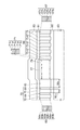
【解決手段】本発明の半導体レーザは、第1光閉じ込め層15と、第1のエリア上に設けられた複数の第1の量子細線17及び埋め込み半導体領域23と、第2のエリア上に設けられた複数の第2の量子細線19及び埋め込み半導体領域25と、第3のエリア15c上に設けられた活性層21と、第2光閉じ込め層31とを有する。第1の量子細線17と埋め込み半導体領域23とは、第1の分布ブラッグ反射器18を構成し、第2の量子細線19と埋め込み半導体領域25とは、第2の分布ブラッグ反射器20を構成する。これらの分布ブラッグ反射器により、活性層21の長さを共振器長とするDBRレーザが形成される。
【選択図】 図2
Description
K. Shinoda et al.:IPRM2007, TuB2-3, 39.
第1クラッド層13:n型InP,Si,1×1018cm−3,厚さ 500nm
第1光閉じ込め層15:n型GaInAsP,Si,5×1017cm−3,厚さ 150nm
第1の量子細線17:第1の井戸層17a及び第1の障壁層17b
第1の井戸層17a:アンドープGaInAsP,厚さ 6nm
第1の障壁層17b:アンドープGaInAsP,厚さ 9nm
第2の量子細線19:第2の井戸層19a及び第1の障壁層19b
第2の井戸層19a:アンドープGaInAsP,厚さ 6nm
第2の障壁層19b:アンドープGaInAsP,厚さ 9nm
活性層21:第3の井戸層21a及び第3の障壁層21b
第3の井戸層21a:アンドープGaInAsP,厚さ 6nm
第3の障壁層21b:アンドープGaInAsP,厚さ 9nm
第3光閉じ込め層17c:アンドープGaInAsP,厚さ 40nm
第4光閉じ込め層19c:アンドープGaInAsP,厚さ 40nm
第5光閉じ込め層29:アンドープGaInAsP,厚さ 40nm
埋め込み半導体領域23,25:アンドープAlInAs
キャリアストップ層27:アンドープAlInAs、厚さ 40nm
第2光閉じ込め層31:p型GaInAsP,Zn,5×1017cm−3,厚さ 110nm
第2クラッド層33:p型InP,Zn,1×1018cm−3,厚さ 2000nm
コンタクト層37:p型GaInAs,Zn,1×1019cm−3,厚さ 500nm
Claims (10)
- 第1〜第3のエリアを含む主面を有し、クラッド領域上に設けられた第1光閉じ込め層と、
前記第1のエリア上に前記所定の軸に沿って配列され、第1の分布ブラッグ反射器のための複数の第1の量子細線と、
前記第2のエリア上に前記所定の軸に沿って配列され、第2の分布ブラッグ反射器のための複数の第2の量子細線と、
前記第1の量子細線の側面の間及び前記第2の量子細線の側面の間に設けられた埋め込み半導体領域と、
前記所定の軸に沿って前記第3のエリアの一端から他端まで延びており、前記第3のエリア上に設けられた活性層と、
前記第1の分布ブラッグ反射器上、前記第2の分布ブラッグ反射器上及び前記活性層上に設けられた第2光閉じ込め層と
を有し、
前記第3のエリアは、前記第1のエリアと前記第2のエリアとの間に設けられており、
前記埋め込み半導体領域は、前記第1の量子細線の平均の屈折率及び前記第2の量子細線の平均の屈折率とは異なる屈折率を有することを特徴とする半導体レーザ。 - 前記所定の軸に沿って取られた各第1の量子細線の幅は、前記所定の軸に沿って取られた各第2の量子細線の幅よりも大きく、
前記第1の分布ブラッグ反射器の前記所定の軸に沿って取られた長さは、前記第2の分布ブラッグ反射器の前記所定の軸に沿って取られた長さよりも長いことを特徴とする請求項1に記載の半導体レーザ。 - 前記第1の量子細線は、交互に配置された第1の井戸層と第1の障壁層とを有し、
前記第2の量子細線は、交互に配置された第2の井戸層と第2の障壁層とを有し、
前記活性層は、交互に配置された第3の井戸層と第3の障壁層とを有し、
前記第1〜第3の井戸層は互いに同じ材料からなり、
前記第1〜第3の障壁層は互いに同じ材料からなることを特徴とする請求項1または請求項2に記載の半導体レーザ。 - 前記活性層の前記所定の軸に沿って取られた長さは、50μm以上100μm以下であることを特徴とする請求項1〜請求項3のいずれか1項に記載の半導体レーザ。
- 前記活性層と前記第2光閉じ込め層との間に設けられたキャリアストップ層を更に備え、
前記クラッド領域はn型半導体からなり、
前記キャリアストップ層は、III族元素としてアルミニウム及びインジウムを含むと共にV族元素としてヒ素を含む半導体材料からなり、
前記第2光閉じ込め層はp型GaInAsP半導体からなり、
前記キャリアストップ層のバンドギャップは、前記第2光閉じ込め層のバンドギャップより大きく、且つ前記活性層の内の最大のバンドギャップより大きいことを特徴とする請求項1〜請求項4のいずれか1項に記載の半導体レーザ。 - 前記活性層と前記第2の分布ブラッグ反射器との間に設けられ、前記埋め込み半導体領域と同じ材料からなるギャップ領域を更に備え、
前記ギャップ領域の前記所定の軸に沿って取られた幅は、前記第2の量子細線の間隔よりも大きいことを特徴とする請求項1〜請求項5のいずれか1項に記載の半導体レーザ。 - 前記活性層上に設けられた電極を更に備えることを特徴とする請求項1〜6のいずれか1項に記載の半導体レーザ。
- 半導体レーザを作製する方法であって、
第1光閉じ込め層をクラッド領域上に成長する工程と、
多重量子井戸のための半導体層を前記第1光閉じ込め層上に成長する工程と、
前記所定の軸の方向に配列された複数の第1の量子細線のための第1のパターンと、前記所定の軸の方向に配列された複数の第2の量子細線のための第2のパターンと、活性層のための第3のパターンとを有するマスクを前記半導体層上に形成する工程と、
前記マスクを用いて前記半導体層をエッチングし、前記活性層、前記第1及び第2の量子細線を形成する工程と、
前記第1及び第2の量子細線を埋め込むために、前記第1の量子細線の側面の間及び前記第2の量子細線の側面の間に埋め込み半導体領域を成長する工程と
を備え、
前記第3のパターンは、前記第1のパターンと前記第2のパターンとの間に設けられていることを特徴とする方法。 - 前記所定の軸に沿って取られた各第1の量子細線の幅は、前記所定の軸に沿って取られた各第2の量子細線の幅よりも大きく、
前記第1の量子細線の配列の前記所定の軸に沿って取られた長さは、前記第2の量子細線の配列の前記所定の軸に沿って取られた長さよりも長いことを特徴とする請求項8に記載の方法。 - 前記半導体層をエッチングした後、且つ前記埋め込み半導体領域を成長する前に前記マスクを除去する工程と、
前記埋め込み半導体領域を成長した後に、第2光閉じ込め層を成長する工程と
を更に備え、
前記埋め込み半導体領域を成長する工程において、前記活性層上にキャリアストップ層を併せて成長し、
前記埋め込み半導体領域及び前記キャリアストップ層は、III族元素としてアルミニウム及びインジウムを含むと共にV族元素としてヒ素を含む半導体材料からなり、
前記クラッド領域はn型半導体からなり、
前記第2光閉じ込め層はp型GaInAsP半導体からなり、
前記埋め込み半導体領域及び前記キャリアストップ層のバンドギャップは、前記第2光閉じ込め層のバンドギャップより大きく、且つ前記活性層の内の最大のバンドギャップより大きく、
前記第2光閉じ込め層は、前記第1の量子細線上、前記第2の量子細線上、前記埋め込み半導体領域及び前記キャリアストップ層上に成長することを特徴とする請求項8または請求項9に記載の方法。
Priority Applications (2)
| Application Number | Priority Date | Filing Date | Title |
|---|---|---|---|
| JP2008207041A JP5051054B2 (ja) | 2008-08-11 | 2008-08-11 | 半導体レーザおよび半導体レーザを作製する方法 |
| US12/464,262 US7957446B2 (en) | 2008-08-11 | 2009-05-12 | Semiconductor laser and method of making semiconductor laser |
Applications Claiming Priority (1)
| Application Number | Priority Date | Filing Date | Title |
|---|---|---|---|
| JP2008207041A JP5051054B2 (ja) | 2008-08-11 | 2008-08-11 | 半導体レーザおよび半導体レーザを作製する方法 |
Publications (2)
| Publication Number | Publication Date |
|---|---|
| JP2010045102A true JP2010045102A (ja) | 2010-02-25 |
| JP5051054B2 JP5051054B2 (ja) | 2012-10-17 |
Family
ID=41652913
Family Applications (1)
| Application Number | Title | Priority Date | Filing Date |
|---|---|---|---|
| JP2008207041A Active JP5051054B2 (ja) | 2008-08-11 | 2008-08-11 | 半導体レーザおよび半導体レーザを作製する方法 |
Country Status (2)
| Country | Link |
|---|---|
| US (1) | US7957446B2 (ja) |
| JP (1) | JP5051054B2 (ja) |
Cited By (4)
| Publication number | Priority date | Publication date | Assignee | Title |
|---|---|---|---|---|
| JP2015535143A (ja) * | 2012-11-01 | 2015-12-07 | オクラロ テクノロジー リミテッド | 半導体dbrレーザ |
| JP2015230974A (ja) * | 2014-06-05 | 2015-12-21 | 住友電気工業株式会社 | 量子カスケード半導体レーザ |
| JP2016197658A (ja) * | 2015-04-03 | 2016-11-24 | 住友電気工業株式会社 | 量子カスケード半導体レーザ |
| JP2018006440A (ja) * | 2016-06-29 | 2018-01-11 | 日本電信電話株式会社 | 半導体レーザ |
Families Citing this family (3)
| Publication number | Priority date | Publication date | Assignee | Title |
|---|---|---|---|---|
| US11362487B2 (en) * | 2020-05-27 | 2022-06-14 | Microsoft Technology Licensing, Llc | Laser emitter including nanowires |
| CN113471812B (zh) * | 2021-07-02 | 2023-10-13 | 中国科学院半导体研究所 | 增益器件、半导体激光器及半导体激光器的制作方法 |
| CN113791416B (zh) * | 2021-09-10 | 2023-12-05 | 苏州长光华芯光电技术股份有限公司 | 一种激光雷达系统 |
Family Cites Families (3)
| Publication number | Priority date | Publication date | Assignee | Title |
|---|---|---|---|---|
| JPS63255985A (ja) | 1987-04-14 | 1988-10-24 | Oki Electric Ind Co Ltd | 分布反射型半導体レ−ザ素子 |
| US6822982B2 (en) * | 2001-09-28 | 2004-11-23 | The Furukawa Electric Co., Ltd. | Device and method for providing a tunable semiconductor laser |
| JP4193866B2 (ja) * | 2006-04-27 | 2008-12-10 | 住友電気工業株式会社 | 半導体発光素子の製造方法 |
-
2008
- 2008-08-11 JP JP2008207041A patent/JP5051054B2/ja active Active
-
2009
- 2009-05-12 US US12/464,262 patent/US7957446B2/en active Active
Cited By (4)
| Publication number | Priority date | Publication date | Assignee | Title |
|---|---|---|---|---|
| JP2015535143A (ja) * | 2012-11-01 | 2015-12-07 | オクラロ テクノロジー リミテッド | 半導体dbrレーザ |
| JP2015230974A (ja) * | 2014-06-05 | 2015-12-21 | 住友電気工業株式会社 | 量子カスケード半導体レーザ |
| JP2016197658A (ja) * | 2015-04-03 | 2016-11-24 | 住友電気工業株式会社 | 量子カスケード半導体レーザ |
| JP2018006440A (ja) * | 2016-06-29 | 2018-01-11 | 日本電信電話株式会社 | 半導体レーザ |
Also Published As
| Publication number | Publication date |
|---|---|
| US7957446B2 (en) | 2011-06-07 |
| US20100034229A1 (en) | 2010-02-11 |
| JP5051054B2 (ja) | 2012-10-17 |
Similar Documents
| Publication | Publication Date | Title |
|---|---|---|
| JP4643794B2 (ja) | 半導体発光素子 | |
| US7941024B2 (en) | Buried heterostructure device having integrated waveguide grating fabricated by single step MOCVD | |
| JP5051054B2 (ja) | 半導体レーザおよび半導体レーザを作製する方法 | |
| US8273585B2 (en) | Optical semiconductor device and method for manufacturing the same | |
| US20090086785A1 (en) | Semiconductor light emitting device and method for manufacturing the same | |
| JP3842976B2 (ja) | 分布帰還型半導体レーザとその製造方法 | |
| JPH0653619A (ja) | 化合物半導体装置及びその製造方法 | |
| JPH08242034A (ja) | 分布帰還型半導体レーザ装置 | |
| JP3204474B2 (ja) | 利得結合分布帰還型半導体レーザとその作製方法 | |
| US20130183784A1 (en) | Method for producing integrated optical device | |
| JP5673253B2 (ja) | 光半導体素子、半導体レーザ、および光半導体素子の製造方法 | |
| JP4599700B2 (ja) | 分布帰還型半導体レーザ | |
| CN215771900U (zh) | 一种多结分布反馈半导体激光器 | |
| JP5310271B2 (ja) | 半導体レーザ素子 | |
| JP2950297B2 (ja) | 分布帰還型半導体レーザ及びその製造方法 | |
| JP4617684B2 (ja) | 半導体レーザ素子 | |
| JP2630035B2 (ja) | 波長可変半導体レーザ | |
| JP2012033975A (ja) | 半導体レーザの作製方法 | |
| JP2010171262A (ja) | 半導体レーザを作製する方法および半導体レーザ | |
| JP5076964B2 (ja) | 半導体レーザおよび半導体レーザを作製する方法 | |
| JP2008198654A (ja) | 半導体レーザ、および半導体レーザを作製する方法 | |
| JPH10270789A (ja) | 光通信等に用いる半導体光素子及びその製造方法 | |
| US20040151224A1 (en) | Distributed feedback semiconductor laser oscillating at longer wavelength mode and its manufacture method | |
| JP2006013191A (ja) | 光半導体素子 | |
| JP2009238796A (ja) | 半導体レーザ及び半導体レーザの作製方法 |
Legal Events
| Date | Code | Title | Description |
|---|---|---|---|
| A621 | Written request for application examination |
Free format text: JAPANESE INTERMEDIATE CODE: A621 Effective date: 20110520 |
|
| A977 | Report on retrieval |
Free format text: JAPANESE INTERMEDIATE CODE: A971007 Effective date: 20120613 |
|
| TRDD | Decision of grant or rejection written | ||
| A01 | Written decision to grant a patent or to grant a registration (utility model) |
Free format text: JAPANESE INTERMEDIATE CODE: A01 Effective date: 20120626 |
|
| A01 | Written decision to grant a patent or to grant a registration (utility model) |
Free format text: JAPANESE INTERMEDIATE CODE: A01 |
|
| A61 | First payment of annual fees (during grant procedure) |
Free format text: JAPANESE INTERMEDIATE CODE: A61 Effective date: 20120709 |
|
| R150 | Certificate of patent or registration of utility model |
Ref document number: 5051054 Country of ref document: JP Free format text: JAPANESE INTERMEDIATE CODE: R150 Free format text: JAPANESE INTERMEDIATE CODE: R150 |
|
| FPAY | Renewal fee payment (event date is renewal date of database) |
Free format text: PAYMENT UNTIL: 20150803 Year of fee payment: 3 |
|
| R250 | Receipt of annual fees |
Free format text: JAPANESE INTERMEDIATE CODE: R250 |
|
| R250 | Receipt of annual fees |
Free format text: JAPANESE INTERMEDIATE CODE: R250 |
|
| R250 | Receipt of annual fees |
Free format text: JAPANESE INTERMEDIATE CODE: R250 |
|
| R250 | Receipt of annual fees |
Free format text: JAPANESE INTERMEDIATE CODE: R250 |
|
| R250 | Receipt of annual fees |
Free format text: JAPANESE INTERMEDIATE CODE: R250 |
|
| R250 | Receipt of annual fees |
Free format text: JAPANESE INTERMEDIATE CODE: R250 |
|
| R250 | Receipt of annual fees |
Free format text: JAPANESE INTERMEDIATE CODE: R250 |
|
| R250 | Receipt of annual fees |
Free format text: JAPANESE INTERMEDIATE CODE: R250 |
|
| R250 | Receipt of annual fees |
Free format text: JAPANESE INTERMEDIATE CODE: R250 |
|
| R250 | Receipt of annual fees |
Free format text: JAPANESE INTERMEDIATE CODE: R250 |
|
| R250 | Receipt of annual fees |
Free format text: JAPANESE INTERMEDIATE CODE: R250 |