JP2010027782A - Light emitting device - Google Patents
Light emitting device Download PDFInfo
- Publication number
- JP2010027782A JP2010027782A JP2008186053A JP2008186053A JP2010027782A JP 2010027782 A JP2010027782 A JP 2010027782A JP 2008186053 A JP2008186053 A JP 2008186053A JP 2008186053 A JP2008186053 A JP 2008186053A JP 2010027782 A JP2010027782 A JP 2010027782A
- Authority
- JP
- Japan
- Prior art keywords
- light emitting
- light
- emitting element
- emitting device
- layer
- Prior art date
- Legal status (The legal status is an assumption and is not a legal conclusion. Google has not performed a legal analysis and makes no representation as to the accuracy of the status listed.)
- Granted
Links
Images


Classifications
-
- H—ELECTRICITY
- H01—ELECTRIC ELEMENTS
- H01L—SEMICONDUCTOR DEVICES NOT COVERED BY CLASS H10
- H01L2224/00—Indexing scheme for arrangements for connecting or disconnecting semiconductor or solid-state bodies and methods related thereto as covered by H01L24/00
- H01L2224/01—Means for bonding being attached to, or being formed on, the surface to be connected, e.g. chip-to-package, die-attach, "first-level" interconnects; Manufacturing methods related thereto
- H01L2224/42—Wire connectors; Manufacturing methods related thereto
- H01L2224/47—Structure, shape, material or disposition of the wire connectors after the connecting process
- H01L2224/48—Structure, shape, material or disposition of the wire connectors after the connecting process of an individual wire connector
- H01L2224/4805—Shape
- H01L2224/4809—Loop shape
- H01L2224/48091—Arched
Landscapes
- Led Device Packages (AREA)
- Led Devices (AREA)
Abstract
Description
本発明は、発光装置に関し、より詳細には、配光特性を制御するための反射部材を備えた発光装置に関する。 The present invention relates to a light emitting device, and more particularly to a light emitting device including a reflecting member for controlling light distribution characteristics.
近年、窒化物半導体を用いた青色発光素子が開発されたことから、発光素子から出力される光の一部を吸収して異なる波長の光を出力する蛍光体と組み合わせることにより、種々の色調の発光色を有する発光装置を作製することが可能となった。特に、発光素子が青色発光素子であり、蛍光体が青色発光素子の発光の一部を吸収して青色の補色に変換すれば、白色系の混色光を発光する発光装置が得られる。
そして、このような発光装置を用いて、携帯電話及びデジタルカメラ等のバックライトに好適に用いることができるように、薄型化及び小型化された角棒状の線状光源装置が提案されている(例えば、特許文献1)。
In recent years, blue light-emitting elements using nitride semiconductors have been developed. By combining with phosphors that absorb part of the light output from the light-emitting elements and output light of different wavelengths, various color tones can be obtained. A light emitting device having an emission color can be manufactured. In particular, if the light-emitting element is a blue light-emitting element and the phosphor absorbs part of the light emitted from the blue light-emitting element and converts it into a blue complementary color, a light-emitting device that emits white mixed light can be obtained.
Then, a rectangular bar-shaped linear light source device has been proposed that can be suitably used for a backlight of a mobile phone, a digital camera or the like using such a light emitting device ( For example, Patent Document 1).
しかし、特許文献1の線状光源装置では、隣接する発光素子間まで、発光素子からの光が十分に広がらない。そのため、隣接する発光素子間が暗部となって、導光板の入射面近傍に明部と暗部が視認され、輝度むらが生じる。
この輝度むらを解消する方法としては、輝度むらが生じないように工夫された導光板を使用して、発光装置からの光を導光板全体に均一に拡げる方法があるが、そのような導光板の製造はコストが高くなる問題がある。
そこで、本発明は、輝度むらが生じないように工夫された導光板を使用せずに、輝度むらの少ない線状光源装置を形成できる発光装置を提供することを目的とする。
However, in the linear light source device of
As a method of eliminating this luminance unevenness, there is a method of using a light guide plate devised so as not to cause luminance unevenness and spreading light from the light emitting device uniformly over the entire light guide plate. There is a problem in that the production of the cost increases.
Therefore, an object of the present invention is to provide a light emitting device capable of forming a linear light source device with less luminance unevenness without using a light guide plate devised so as not to cause luminance unevenness.
本発明は、上記課題に鑑みなされたものであり、発光素子を用いて、特に、線状光源装置の場合においても、線状光源装置の中心部から端部にわたって、光を広げることが可能な発光装置を提供する。
そして、複数個の発光素子を並べた場合は、発光素子と発光素子の間まで発光素子からの光が届く発光装置を提供することを目的とする。
The present invention has been made in view of the above-described problems, and it is possible to spread light using a light-emitting element, particularly in the case of a linear light source device, from the center to the end of the linear light source device. A light emitting device is provided.
An object of the present invention is to provide a light-emitting device in which light from a light-emitting element reaches between the light-emitting elements when a plurality of light-emitting elements are arranged.
本発明の発光装置は、基板と、該基板に載置された発光素子と、前記発光素子を挟むように前記基板に設けられる一対の反射部材と、
該発光素子と前記一対の反射部材の少なくとも一部を被覆する透光性部材とを備えた発光装置であって、
前記透光性部材は、前記発光装置の側面において露出する第1の側面及び該第1の側面と対面する第2の側面を有しており、前記発光素子の上方に、第1の側面から第2の側面まで延伸する溝部を有することを特徴とする。
このような発光装置では、
前記溝部は、側面視においてV字形状であり、前記基板表面に対して20°から45°傾斜する対向面を有することが好ましい。
前記対向面は、その少なくとも一部が発光素子直上に配置されることが好ましい。
前記透光性部材は、前記発光素子を被覆する第1層と該第1層を被覆する第2層を含み、前記第1層に蛍光体を含むことが好ましい。
前記発光素子は前記基板に複数配置され、各発光素子に対して前記一対の反射部材がそれぞれ配置されてなることが好ましい。
前記反射部材がトランスファモールドによって形成されてなることが好ましい。
前記反射部材は、角度の異なる反射面を少なくとも2面有することが好ましい。
A light emitting device of the present invention includes a substrate, a light emitting element placed on the substrate, a pair of reflecting members provided on the substrate so as to sandwich the light emitting element,
A light emitting device comprising the light emitting element and a translucent member covering at least a part of the pair of reflecting members,
The translucent member has a first side surface exposed on a side surface of the light emitting device and a second side surface facing the first side surface, and the first side surface is disposed above the light emitting element. It has the groove part extended to a 2nd side surface, It is characterized by the above-mentioned.
In such a light emitting device,
It is preferable that the groove has a V shape in a side view and has a facing surface inclined by 20 ° to 45 ° with respect to the substrate surface.
It is preferable that at least a part of the facing surface is disposed immediately above the light emitting element.
The translucent member preferably includes a first layer covering the light emitting element and a second layer covering the first layer, and the first layer preferably includes a phosphor.
It is preferable that a plurality of the light emitting elements are arranged on the substrate, and the pair of reflecting members are arranged for each light emitting element.
It is preferable that the reflection member is formed by transfer molding.
The reflecting member preferably has at least two reflecting surfaces with different angles.
本発明の発光装置によれば、発光素子を用いて、光源の中心部から端部にわたって光の分布が広げられた発光装置を提供することができる。 According to the light emitting device of the present invention, it is possible to provide a light emitting device in which the light distribution is widened from the center to the end of the light source using the light emitting element.
本発明の発光装置は、図1に示したように、主として、基板10、発光素子11、発光素子を被覆する透光性部材12、透光性部材に設けられた溝部22、一対の反射部材13を備えて構成されている。なお、本発明の発光装置を線状光源装置として利用することもできる。
As shown in FIG. 1, the light emitting device of the present invention mainly includes a
(基板)
基板は、適当な機械的強度と絶縁性を有する材料であればどのような材料によって形成されていてもよい。例えば、BTレジン、ガラスエポキシ等のプラスチック、硝子、セラミック等からなる絶縁基板が挙げられる。中でも、酸化アルミニウム質焼結体(アルミナセラミックス)、窒化アルミニウム質焼結体、ガラスセラミックス等のセラミックス等からなるものが、発光素子を支持するための支持部材および発光素子の熱を放熱させるための放熱部材として機能し得るために好適である。通常、上面が平坦で、略直方体形状を有している。なお、基板は、単一層によって形成されていてもよいし、表面に導電膜によるパターンを備えた複数の層を貼り合せた積層基板を用いてもよい。
(電極)
基板上には、負及び正電極が所定の間隔をあけて形成されている。負及び正電極は、Cuを主成分とする金属層とすることが好ましい。具体的には、Cu/Ni/Ag等が挙げられる。また、負電極及び正電極は、絶縁基板の裏面に形成された実装基板接続用の電極と貫通孔(図示せず)を介して接続されていることが好ましい。これにより、フレキシブル基板との電気的接続を図る。
(substrate)
The substrate may be formed of any material as long as the material has appropriate mechanical strength and insulation. For example, an insulating substrate made of BT resin, plastic such as glass epoxy, glass, ceramic, or the like can be given. Among them, an aluminum oxide sintered body (alumina ceramic), an aluminum nitride sintered body, ceramics such as glass ceramics, and the like are used to support the light emitting element and to dissipate heat from the light emitting element. It is suitable because it can function as a heat dissipation member. Usually, the upper surface is flat and has a substantially rectangular parallelepiped shape. Note that the substrate may be formed of a single layer, or a laminated substrate in which a plurality of layers having a conductive film pattern on the surface are bonded.
(electrode)
On the substrate, negative and positive electrodes are formed at predetermined intervals. The negative and positive electrodes are preferably metal layers mainly composed of Cu. Specifically, Cu / Ni / Ag etc. are mentioned. Moreover, it is preferable that the negative electrode and the positive electrode are connected to a mounting substrate connecting electrode formed on the back surface of the insulating substrate through a through hole (not shown). Thereby, electrical connection with a flexible substrate is aimed at.
(発光素子)
発光素子は、半導体発光素子であればよく、いわゆる発光ダイオードと呼ばれる素子であればどのようなものでもよい。発光素子は、1つの発光装置に1つのみ搭載されていてもよいが、複数個搭載されていることが好ましい。これにより、線方向により輝度が均一化された発光装置を得られる。この場合には、発光素子は、基板にマトリックス状に配置されていることが好ましい。薄型化しつつ輝度の高い発光装置を提供することができるからである。
発光素子は、例えば、基板上に、InN、AlN、GaN、InGaN、AlGaN、InGaAlN等の窒化物半導体、III−V族化合物半導体、II−VI族化合物半導体等、種々の半導体によって、活性層を含む積層構造が形成されたものが挙げられる。
(Light emitting element)
The light emitting element may be a semiconductor light emitting element, and any element may be used as long as it is an element called a light emitting diode. Although only one light emitting element may be mounted on one light emitting device, a plurality of light emitting elements are preferably mounted. As a result, a light emitting device having uniform luminance in the line direction can be obtained. In this case, the light emitting elements are preferably arranged in a matrix on the substrate. This is because a light-emitting device with high luminance can be provided while being thinned.
The light emitting device has an active layer formed on a substrate by various semiconductors such as nitride semiconductors such as InN, AlN, GaN, InGaN, AlGaN, InGaAlN, III-V compound semiconductors, II-VI compound semiconductors, and the like. The thing in which the laminated structure containing was formed is mentioned.
例えば、後述する蛍光体と組み合わせて、白色系の光を発する発光装置を構成するために適した発光素子として、窒化物半導体(InXAlYGa1−X−YN、0≦X、0≦Y、X+Y≦1)を用いたものが適している。この発光素子は、InZGa1−ZN(0<Z<1)を発光層として有しており、その混晶度によって発光波長を約365nmから650nmで任意に変えることができる。 For example, as a light-emitting element suitable for forming a light-emitting device that emits white light in combination with a phosphor described later, a nitride semiconductor (In X Al Y Ga 1- XYN, 0 ≦ X, 0 Those using ≦ Y, X + Y ≦ 1) are suitable. The light-emitting element, In Z Ga 1-Z N has a (0 <Z <1) as a luminescent layer, it is possible to arbitrarily change at 650nm with emission wavelength of about 365nm by the degree of the mixed crystal.
発光素子を構成する基板としては、サファイアやスピネル(MgA12O4)のような絶縁性基板、また炭化珪素、Si、ZnS、ZnO、GaAs、ダイヤモンド;ニオブ酸リチウム、ガリウム酸ネオジウム等の酸化物基板、窒化物半導体基板(GaN、AlN等)等が挙げられる。
発光層には、Si、Ge等のドナー不純物及び/又はZn、Mg等のアクセプター不純物がドープされる場合もある。
As a substrate constituting the light emitting element, an insulating substrate such as sapphire and spinel (MgA1 2 O 4 ), silicon carbide, Si, ZnS, ZnO, GaAs, diamond; oxide such as lithium niobate and neodymium gallate Examples include substrates and nitride semiconductor substrates (GaN, AlN, etc.).
The light emitting layer may be doped with donor impurities such as Si and Ge and / or acceptor impurities such as Zn and Mg.
発光素子の発光波長は、半導体の材料、混晶比、発光層のInGaNのIn含有量、発光層にドープする不純物の種類を変化させるなどによって、紫外領域から赤色まで変化させることができる。 特に、白色系の光を発光させるために、発光波長が400nm以上530nm以下に設定することが好ましく、420nm以上490nm以下に設定することがより好ましい。なお、蛍光体の種類を選択することにより、400nmより短い紫外領域の波長の光を発光する発光素子を用いることもできる。 The emission wavelength of the light-emitting element can be changed from the ultraviolet region to red by changing the semiconductor material, the mixed crystal ratio, the In content of InGaN in the light-emitting layer, and the type of impurities doped in the light-emitting layer. In particular, in order to emit white light, the emission wavelength is preferably set to 400 nm or more and 530 nm or less, and more preferably set to 420 nm or more and 490 nm or less. Note that a light-emitting element that emits light having a wavelength in the ultraviolet region shorter than 400 nm can be used by selecting the type of phosphor.
発光素子は、通常、基板上に形成された負及び正電極に、それぞれワイヤにより接続されている。ワイヤとしては、発光素子の電極とのオーミック性が良好であるか、機械的接続性が良好であるか、電気伝導性及び熱伝導性が良好なものであることが好ましい。熱伝導率としては、0.01cal/S・cm2・℃/cm程度以上が好ましく、さらに0.5cal/S・cm2・℃/cm程度以上がより好ましい。作業性などを考慮すると、ワイヤの直径は、10μm〜45μm程度であることが好ましい。このようなワイヤとしては、例えば、金、銅、白金、アルミニウム等の金属及びそれらの合金が挙げられる。
発光素子は、ワイヤーボンディングの他、半田等の導電性接着部材を用いてフリップチップボンディングしてもよい。
The light emitting element is usually connected to negative and positive electrodes formed on a substrate by wires. The wire preferably has good ohmic properties with the electrode of the light emitting element, good mechanical connectivity, or good electrical and thermal conductivity. The thermal conductivity, preferably 0.01cal / S · cm 2 · ℃ / than about cm further 0.5cal / S · cm 2 · ℃ / cm or higher order is more preferable. Considering workability and the like, the diameter of the wire is preferably about 10 μm to 45 μm. Examples of such wires include metals such as gold, copper, platinum, and aluminum, and alloys thereof.
The light emitting element may be flip-chip bonded using a conductive adhesive member such as solder in addition to wire bonding.
(透光性部材)
透光性部材は、発光素子を外部環境から保護する機能を有する。
本発明において、透光性部材は、発光装置の側面において露出する第1の側面及び該第1の側面と対面する第2の側面を有しており、発光素子の上方に位置する表面(光取出面)において、第1の側面から第2の側面まで延伸する溝部を有する。また、発光素子を複数配置する場合は、各発光素子に対して、溝部がそれぞれ形成されている事が好ましい。このような構成により、観察方向によって生じる輝度むらを低減することができる。
(Translucent member)
The translucent member has a function of protecting the light emitting element from the external environment.
In the present invention, the translucent member has a first side surface exposed on the side surface of the light emitting device and a second side surface facing the first side surface, and is a surface (light) located above the light emitting element. The extraction surface has a groove extending from the first side surface to the second side surface. Further, when a plurality of light emitting elements are arranged, it is preferable that a groove is formed for each light emitting element. With such a configuration, luminance unevenness caused by the observation direction can be reduced.
透光性部材を構成する材料は特に限定されるものではなく、例えば、用いる発光素子が発光する光の80%以上、好ましくは85%以上、より好ましくは90%以上、95%以上を透過させる材料であることが適している。具体的には、エポキシ樹脂、シリコーン樹脂、変成シリコーン樹脂、ウレタン樹脂、オキセタン樹脂、アクリル樹脂、ポリカーボネイト、ポリイミド樹脂などの透光性樹脂や、ガラスなどの透光性無機材料が挙げられる。なかでも、エポキシ樹脂、シリコーン樹脂、変成シリコーン樹脂、オキセタン樹脂を用いることが好ましい。 There is no particular limitation on the material forming the light-transmitting member, and for example, 80% or more, preferably 85% or more, more preferably 90% or more, 95% or more of the light emitted from the light emitting element to be used is transmitted. The material is suitable. Specifically, a translucent resin such as an epoxy resin, a silicone resin, a modified silicone resin, a urethane resin, an oxetane resin, an acrylic resin, a polycarbonate, or a polyimide resin, or a translucent inorganic material such as glass can be given. Among these, it is preferable to use an epoxy resin, a silicone resin, a modified silicone resin, or an oxetane resin.
透光性部材は、上述した材料の単層で形成されていてもよいし、上述した材料の全体にわたって蛍光体を含んだ単層で形成されていてもよい。少なくとも発光素子(好ましくは、発光素子に接続されるワイヤをも含んで)を被覆する第1層と、これを被覆する第2層を含むような2層以上の積層構造であることが好ましい。この場合、第1層に蛍光体を含み、この第1層上に、実質的に蛍光体を含まない第2層とから構成される積層構造であることがより好ましい。
第2層にも蛍光体を含む場合、透光性部材全体に発光素子及び蛍光体の混色光が散乱され、溝部による効果が薄れる。しかし、このように発光素子の極近くにのみ蛍光体を配置させることによって、発光素子及び蛍光体の混色光の発光領域を小さくし、混色光を溝部に導光させることができる。
特に、積層構造で形成する場合には、第1層目の透光性部材の粘度は、硬化前で100〜2000mPa・sであることが好ましい。ここで「粘度」は、円錐平板型回転粘度計を用い、常温下で測定したものを指す。また、第1層は、硬化条件が80℃〜180℃、数分〜数時間の下で形状を維持できる程度の硬さになる樹脂であることが好ましい。これにより、第1層目の透光性部材を、発光素子の周辺にのみ、塗布等という簡便な方法により、容易に形成することができる。
The translucent member may be formed of a single layer of the above-described material, or may be formed of a single layer including a phosphor throughout the above-described material. A laminated structure of two or more layers including at least a first layer covering a light emitting element (preferably including a wire connected to the light emitting element) and a second layer covering the light emitting element is preferable. In this case, it is more preferable that the first layer has a laminated structure including a phosphor and a second layer substantially not containing the phosphor on the first layer.
In the case where the second layer also contains a phosphor, the mixed light of the light emitting element and the phosphor is scattered throughout the translucent member, and the effect of the groove portion is reduced. However, by arranging the phosphor only in the vicinity of the light emitting element in this way, the light emission region of the mixed color light of the light emitting element and the phosphor can be reduced, and the mixed color light can be guided to the groove portion.
In particular, when forming with a laminated structure, it is preferable that the translucent member of the first layer is 100 to 2000 mPa · s before curing. Here, “viscosity” refers to that measured at room temperature using a conical plate type rotational viscometer. The first layer is preferably a resin having a hardness that can maintain the shape under curing conditions of 80 ° C. to 180 ° C. and several minutes to several hours. Thereby, the translucent member of the first layer can be easily formed only around the light emitting element by a simple method such as coating.
透光性部材に形成される溝部の形状は、用いる発光素子の大きさ及び種類等、後述する反射部材の形状及び大きさ等、発光装置自体の形状及び大きさ等によって適宜調整することができる。なお、本実施の形態において、溝部は側面視においてV字形状である。溝部の側面視における形状は、V字に限定されるものではなく、U字、W字、半円形状、半楕円形状及びこれらと近似の形状をとる事もできる。
溝部のV字形状は、対向面が、V字溝の稜線に対して対称であることが好ましい。また、V字溝は、基板表面に対して、20°程度から45°程度傾斜する対向面を有していることが好ましい。複数の発光素子に対して、各々V字溝を設けた場合、基板表面に対して各々略等しい角度で傾斜する対向面を有する事が好ましい。このような角度に設定することにより、発光素子から出射されてV字溝に当たる光を全反射させることができ、より効率的に発光素子からの光を広げることができる。その結果、例えば、線状光源装置において、発光素子の間隔を広げた場合、つまり、用いる発光素子の数を減少した場合においても、光取出面における輝度むらを低減させることが可能となる。
The shape of the groove formed in the translucent member can be appropriately adjusted depending on the shape and size of the light emitting device itself, such as the size and type of the light emitting element to be used, the shape and size of the reflecting member to be described later. . In the present embodiment, the groove is V-shaped when viewed from the side. The shape of the groove portion in a side view is not limited to the V shape, and may be a U shape, a W shape, a semicircular shape, a semielliptical shape, or an approximate shape thereof.
As for the V shape of a groove part, it is preferable that an opposing surface is symmetrical with respect to the ridgeline of a V-shaped groove. Moreover, it is preferable that the V-shaped groove has a facing surface inclined by about 20 ° to 45 ° with respect to the substrate surface. When a V-shaped groove is provided for each of the plurality of light emitting elements, it is preferable to have opposing surfaces that are inclined at substantially the same angle with respect to the substrate surface. By setting such an angle, the light emitted from the light emitting element and hitting the V-shaped groove can be totally reflected, and the light from the light emitting element can be spread more efficiently. As a result, for example, in the linear light source device, even when the interval between the light emitting elements is widened, that is, when the number of light emitting elements to be used is reduced, it is possible to reduce the luminance unevenness on the light extraction surface.
また、溝部の深さW1は、特に限定されるものではなく、透光性部材自体の厚さによって適宜調整することができるが、例えば、透光性部材の全厚みの60〜75%程度、別の観点から、発光素子からの距離が0.15〜0.3mm程度となる深さ、さらに具体的には溝部の深さW1が0.6〜0.8mm程度が挙げられる。
V字溝の場合は、その対向面の少なくとも一部が発光素子の直上に配置され、第1層からの距離が0.05mm〜0.15mm程度で、距離が近い程よい。これにより、発光装置の発光素子の上方に位置する表面(光取出面)において、均一に光を取り出すことができる。
また、溝部の幅W2は、光取出面において異なる幅で形成されてもよいし略同じ幅で形成されてもよい。何れの場合も発光素子及び蛍光体の混色光を発光装置の端部まで広げる事が可能となる。
Further, the depth W1 of the groove is not particularly limited and can be appropriately adjusted depending on the thickness of the translucent member itself. For example, about 60 to 75% of the total thickness of the translucent member, From another viewpoint, the depth at which the distance from the light emitting element is about 0.15 to 0.3 mm, more specifically, the depth W1 of the groove is about 0.6 to 0.8 mm.
In the case of the V-shaped groove, at least a part of the facing surface is disposed immediately above the light emitting element, the distance from the first layer is about 0.05 mm to 0.15 mm, and the closer the distance is. Thereby, light can be extracted uniformly on the surface (light extraction surface) located above the light emitting element of the light emitting device.
Further, the width W2 of the groove may be formed with a different width on the light extraction surface or may be formed with substantially the same width. In either case, it is possible to spread mixed color light of the light emitting element and the phosphor to the end of the light emitting device.
溝部の製造方法は、例えば、溝部の形状に成形された型に、熱硬化性の液状の透光性部材を充填し、その後加熱硬化して得る方法、透光性部材を枠体の内側に充填し、半硬化状態のうちに溝部を形成する位置に溝部の形状の成形型を配置し、透光性部材を硬化後、型から取り出す方法等が挙げられる。 The method of manufacturing the groove part includes, for example, a method in which a mold formed into the shape of the groove part is filled with a thermosetting liquid translucent member and then heated and cured, and the translucent member is placed inside the frame body. Examples thereof include a method of filling a mold part in the shape of a groove part at a position where the groove part is formed in a semi-cured state, and taking out the translucent member from the mold after curing.
なお、透光性部材において、第1層に蛍光体が含まれ、第2層に蛍光体が含まれていない層が積層されている場合には、発光装置の側面において露出する第1の側面及び該第1の側面と対面する第2の側面において、第1層及び第2層が略面一に裁断され、第1層の一部が露出していることが好ましい。これにより、第2層のレンズ特性に殆ど影響を与えることなく、色調を補正することが可能である。すなわち、第1層の側面を研磨する等して第1の側面から第2の側面までの距離を変化させることにより、蛍光体の量も変化させることができる。また、蛍光体を含む透光性部材の厚みを調整して、集合基板をダイシングしても、同様である。これによって発光素子と蛍光体との発光強度比を変えることができるため、色調の補正を行うことができる。一方で、第1層の側面を研磨して透光性部材の厚みを変化させても、第2層の形状は殆ど変化しないため、レンズ特性に影響を与えることなく、色調の補正が可能となる。 In the translucent member, the first side surface exposed on the side surface of the light emitting device when the first layer includes a phosphor and the second layer includes a layer not including the phosphor. In the second side face facing the first side face, it is preferable that the first layer and the second layer are cut to be substantially flush and a part of the first layer is exposed. As a result, it is possible to correct the color tone with little influence on the lens characteristics of the second layer. That is, the amount of the phosphor can be changed by changing the distance from the first side surface to the second side surface by, for example, polishing the side surface of the first layer. The same applies to the case where the aggregate substrate is diced by adjusting the thickness of the translucent member containing the phosphor. As a result, the emission intensity ratio between the light emitting element and the phosphor can be changed, so that the color tone can be corrected. On the other hand, even if the thickness of the translucent member is changed by polishing the side surface of the first layer, the shape of the second layer hardly changes, so that the color tone can be corrected without affecting the lens characteristics. Become.
特に、第1層は、発光素子の光取出面側に凸形状であることが好ましい。そして、透光性部材の第1層は、略半円柱状であり、第1層の露出面に平行な断面(=光取出面に直交する断面)が半円状又は半楕円状となることが好ましい。これによって観察方位による色むらを小さくすることができる。 In particular, the first layer is preferably convex on the light extraction surface side of the light emitting element. The first layer of the translucent member is substantially semi-cylindrical, and the cross section parallel to the exposed surface of the first layer (= the cross section orthogonal to the light extraction surface) is semicircular or semielliptical. Is preferred. As a result, color unevenness due to the viewing direction can be reduced.
透光性部材には、フィラー及び拡散剤等が含まれていてもよい。フィラーとしては、SiO2等が挙げられ、照射された光を反射、散乱させることができる。また、混色が良好になるとともに色むらを低減させることができる。さらに、波長変換部材にフィラーを混合することにより、その粘度を調整することができるため、任意の形状に、任意の部位に、容易に配置させることができる。拡散剤は、光を拡散させるものであり、発光素子からの指向性を緩和させ、視野角を増大させることができる。 The translucent member may contain a filler, a diffusing agent, and the like. Examples of the filler include SiO 2 and can irradiate and scatter the irradiated light. In addition, color mixing can be improved and color unevenness can be reduced. Furthermore, since the viscosity can be adjusted by mixing a filler with the wavelength conversion member, it can be easily placed in any shape and in any part. The diffusing agent diffuses light and can reduce the directivity from the light emitting element and increase the viewing angle.
(蛍光体)
蛍光体は、発光素子からの光を吸収し、異なる波長の光に波長変換するものであればよい。例えば、Eu、Ce等のランタノイド系元素で主に賦活される窒化物系蛍光体・酸窒化物系蛍光体、Eu等のランタノイド系、Mn等の遷移金属系の元素により主に付活されるアルカリ土類ハロゲンアパタイト蛍光体、アルカリ土類金属ホウ酸ハロゲン蛍光体、アルカリ土類金属アルミン酸塩蛍光体、アルカリ土類ケイ酸塩、アルカリ土類硫化物、アルカリ土類チオガレート、アルカリ土類窒化ケイ素、ゲルマン酸塩、又は、Ce等のランタノイド系元素で主に付活される希土類アルミン酸塩、希土類ケイ酸塩又はEu等のランタノイド系元素で主に賦活される有機及び有機錯体等から選ばれる少なくともいずれか1以上であることが好ましい。
(Phosphor)
The phosphor is not limited as long as it absorbs light from the light-emitting element and converts the light into light having a different wavelength. For example, it is mainly activated by nitride-based phosphors / oxynitride-based phosphors mainly activated by lanthanoid elements such as Eu and Ce, lanthanoid-based phosphors such as Eu, and transition metal elements such as Mn. Alkaline earth halogen apatite phosphor, alkaline earth metal borate phosphor, alkaline earth metal aluminate phosphor, alkaline earth silicate, alkaline earth sulfide, alkaline earth thiogallate, alkaline earth nitriding Selected from silicon, germanate, or rare earth aluminate mainly activated by lanthanoid elements such as Ce, organic and organic complexes mainly activated by lanthanoid elements such as rare earth silicate or Eu It is preferable that it is at least any one or more.
Eu、Ce等のランタノイド系元素で主に賦活される窒化物系蛍光体は、M2Si5N8:Eu(Mは、Sr、Ca、Ba、Mg、Znから選ばれる少なくとも1種以上である。以下同義)などがある。また、M2Si5N8:EuのほかMSi7N10:Eu、M1.8Si5O0.2N8:Eu、M0.9Si7O0.1N10:Eu(Mは、Sr、Ca、Ba、Mg、Znから選ばれる少なくとも1種以上である。)などもある。 A nitride phosphor mainly activated by a lanthanoid element such as Eu or Ce is M 2 Si 5 N 8 : Eu (M is at least one selected from Sr, Ca, Ba, Mg, Zn). There is the same meaning). In addition to M 2 Si 5 N 8 : Eu, MSi 7 N 10 : Eu, M 1.8 Si 5 O 0.2 N 8 : Eu, M 0.9 Si 7 O 0.1 N 10 : Eu (M Is at least one selected from Sr, Ca, Ba, Mg, and Zn.
Eu、Ce等のランタノイド系元素で主に賦活される酸窒化物系蛍光体は、MSi2O2N2:Euなどがある。 An oxynitride phosphor mainly activated by a lanthanoid element such as Eu or Ce includes MSi 2 O 2 N 2 : Eu.
Eu等のランタノイド系、Mn等の遷移金属系の元素により主に付活されるアルカリ土類ハロゲンアパタイト蛍光体には、M5(PO4)3X:R(Xは、F、Cl、Br、Iから選ばれる少なくとも1種以上である。Rは、Eu、Mn、Eu及びMnのいずれか1種以上である。X及びRの定義について以下同義)などがある。 Alkaline earth halogen apatite phosphors mainly activated by lanthanoid compounds such as Eu and transition metal elements such as Mn include M 5 (PO 4 ) 3 X: R (X is F, Cl, Br) And at least one selected from I. R is any one or more of Eu, Mn, Eu and Mn.
アルカリ土類金属ホウ酸ハロゲン蛍光体には、M2B5O9X:Rなどがある。
アルカリ土類金属アルミン酸塩蛍光体には、SrAl2O4:R、Sr4Al14O25:R、CaAl2O4:R、BaMg2Al16O27:R、BaMg2Al16O12:R、BaMgAl10O17:Rなどがある。
アルカリ土類硫化物蛍光体には、La2O2S:Eu、Y2O2S:Eu、Gd2O2S:Euなどがある。
Alkaline earth metal borate phosphors include M 2 B 5 O 9 X: R.
Alkaline earth metal aluminate phosphors include SrAl 2 O 4 : R, Sr 4 Al 14 O 25 : R, CaAl 2 O 4 : R, BaMg 2 Al 16 O 27 : R, BaMg 2 Al 16 O 12 : R, BaMgAl 10 O 17 : R and the like.
Examples of the alkaline earth sulfide phosphor include La 2 O 2 S: Eu, Y 2 O 2 S: Eu, and Gd 2 O 2 S: Eu.
Ce等のランタノイド系元素で主に賦活される希土類アルミン酸塩蛍光体には、Y3Al5O12:Ce、(Y0.8Gd0.2)3Al5O12:Ce、Y3(Al0.8Ga0.2)5O12:Ce、(Y,Gd)3(Al,Ga)5O12の組成式で表されるYAG系蛍光体などがある。また、Yの一部又は全部をTb、Lu等で置換したTb3Al5O12:Ce、Lu3Al5O12:Ceなどもある。 Examples of rare earth aluminate phosphors mainly activated with lanthanoid elements such as Ce include Y 3 Al 5 O 12 : Ce, (Y 0.8 Gd 0.2 ) 3 Al 5 O 12 : Ce, Y 3 (Al 0.8 Ga 0.2) 5 O 12: Ce, and the like (Y, Gd) 3 (Al , Ga) YAG -based phosphor represented by the composition formula of 5 O 12. Further, there are Tb 3 Al 5 O 12 : Ce, Lu 3 Al 5 O 12 : Ce, etc. in which a part or all of Y is substituted with Tb, Lu, or the like.
その他の蛍光体には、ZnS:Eu、Zn2GeO4:Mn、MGa2S4:Euなどがある。
上述の蛍光体は、所望に応じてEuに代えて又はEuに加えてTb、Cu、Ag、Au、Cr、Nd、Dy、Co、Ni、Tiから選択される1種以上を含有させることもできる。
Other phosphors include ZnS: Eu, Zn 2 GeO 4 : Mn, MGa 2 S 4 : Eu, and the like.
The above-described phosphor may contain one or more selected from Tb, Cu, Ag, Au, Cr, Nd, Dy, Co, Ni, Ti instead of Eu or in addition to Eu as desired. it can.
Ca−Al−Si−O−N系オキシ窒化物ガラス蛍光体とは、モル%表示で、CaCO3をCaOに換算して20〜50モル%、Al2O3を0〜30モル%、SiOを25〜60モル%、AlNを5〜50モル%、希土類酸化物または遷移金属酸化物を0.1〜20モル%とし、5成分の合計が100モル%となるオキシ窒化物ガラスを母体材料とした蛍光体である。なお、オキシ窒化物ガラスを母体材料とした蛍光体では、窒素含有量が15wt%以下であることが好ましく、希土類酸化物イオンの他に増感剤となる他の希土類元素イオンを希土類酸化物として蛍光ガラス中に0.1〜10モル%の範囲の含有量で共賦活剤として含むことが好ましい。 The Ca—Al—Si—O—N-based oxynitride glass phosphor is expressed in terms of mol%, CaCO 3 is converted to CaO, 20 to 50 mol%, Al 2 O 3 is 0 to 30 mol%, SiO 25 to 60 mol%, AlN 5 to 50 mol%, rare earth oxide or transition metal oxide 0.1 to 20 mol%, and oxynitride glass having a total of 5 components of 100 mol% as a base material This is a phosphor. In addition, in a phosphor using oxynitride glass as a base material, the nitrogen content is preferably 15 wt% or less, and other rare earth element ions serving as a sensitizer in addition to rare earth oxide ions are used as rare earth oxides. It is preferable to contain as a co-activator in content in the range of 0.1-10 mol% in fluorescent glass.
(反射部材)
反射部材は、発光素子や蛍光体からの光を反射させ、所望の方向に取り出すために機能する。
一対の反射部材は、それぞれ、発光素子の側面に対面し、発光素子を挟むように配置されている。また、発光素子が基板に複数個配置された場合、各発光素子に対して一対の反射部材がそれぞれ配置されている事が好ましい。このような構成により、溝部により発光素子と発光素子の間まで広げられた光を所望の方向に取り出すことができる。そして、反射部材は、いずれも、発光素子(上述した透光性部材の第1層を形成する場合には、その第1層の下端部の外縁から、その下端部の外縁)から離間されて、発光素子に対して対称に配置されていることが好ましい。
発光素子を挟むように配置される一対の反射部材間の距離、反射部材の傾斜角、反射部材の高さ等は、用いる発光素子の種類及び大きさ、得ようとする発光装置の配向特性及び性能等によって、適宜調整することができる。
(Reflective member)
The reflecting member functions to reflect light from the light emitting element or the phosphor and extract it in a desired direction.
The pair of reflecting members are respectively arranged so as to face the side surfaces of the light emitting element and sandwich the light emitting element. Further, when a plurality of light emitting elements are arranged on the substrate, it is preferable that a pair of reflecting members is arranged for each light emitting element. With such a configuration, light spread between the light emitting elements by the groove can be extracted in a desired direction. The reflecting members are all separated from the light emitting element (when forming the first layer of the above-described translucent member, from the outer edge of the lower end portion of the first layer to the outer edge of the lower end portion thereof). The light emitting elements are preferably arranged symmetrically.
The distance between a pair of reflecting members arranged so as to sandwich the light emitting element, the inclination angle of the reflecting member, the height of the reflecting member, etc. are the type and size of the light emitting element to be used, the orientation characteristics of the light emitting device to be obtained, and It can be appropriately adjusted depending on performance and the like.
反射面は、基板表面に対して傾斜面を有している。この場合の傾斜角α(図1参照)は、例えば、基板表面に対して10°〜70°程度、さらに45°〜60°程度であることが好ましい。このような傾斜を有していることにより、所望の配光を得ることができる。
また、反射面は、少なくとも角度の異なる2面を有する事が好ましい。この場合、例えば、傾斜角αは、発光素子により近い位置に基板表面に対して、40°〜70°程度の反射面と、発光素子により遠い位置に基板表面に対して、45°〜60°程度の反射面が形成される事が好ましい。そして、上記2つの反射面の間には、基板と略平行な面が形成され、連続面を形成している事が好ましい。さらに、発光素子により近い位置に形成される反射面は、発光素子により遠い位置に形成される反射面よりも基板表面に対して傾斜角が大きいことが好ましい。このような構成により、より確実に所望の配光を得ることができる。
The reflecting surface has an inclined surface with respect to the substrate surface. In this case, the inclination angle α (see FIG. 1) is, for example, preferably about 10 ° to 70 °, more preferably about 45 ° to 60 ° with respect to the substrate surface. By having such an inclination, a desired light distribution can be obtained.
Moreover, it is preferable that a reflective surface has two surfaces from which an angle differs at least. In this case, for example, the inclination angle α is approximately 40 ° to 70 ° with respect to the substrate surface at a position closer to the light emitting element and 45 ° to 60 ° with respect to the substrate surface at a position farther from the light emitting element. It is preferable that a reflective surface of a degree is formed. And it is preferable that a surface substantially parallel to the substrate is formed between the two reflecting surfaces to form a continuous surface. Furthermore, it is preferable that the reflection surface formed at a position closer to the light emitting element has a larger inclination angle with respect to the substrate surface than the reflection surface formed at a position farther from the light emitting element. With such a configuration, a desired light distribution can be obtained more reliably.
反射部材は、上述した第1層の高さよりも低い位置又は高い位置又は同じ高さのいずれに配置されていてもよいが、高い位置に配置されていることが好ましい。同時に、第2層の高さよりも低いが、溝部の最も深い位置より高いことが好ましい。
具体的には、反射部材の高さは、透光性部材の高さに対し90〜100%程度が適当である。
The reflecting member may be arranged at a position lower or higher than the height of the first layer described above or at the same height, but is preferably arranged at a higher position. At the same time, it is preferably lower than the height of the second layer but higher than the deepest position of the groove.
Specifically, the height of the reflecting member is appropriately about 90 to 100% with respect to the height of the translucent member.
反射部材の少なくとも反射面は、発光素子からの光を反射し得る材料で形成されているのであれば、どのような材料を用いてもよい。つまり、反射部材自体を反射率の高い酸化チタン等の白色系の材料で形成したり、反射部材の少なくとも反射面を金属材料で被覆したりしてもよい。金属材料として、例えば、銀、金、銅、アルミニウム、パラジウム、ロジウム又はこれらの合金や積層体等が挙げられる。なお、反射部材と第1層との間の基板表面あるいは反射部材の反射面の少なくとも一方は、上記金属材料が配置されることなく、基板の材料である樹脂が露出されていることが好ましい。樹脂を材料とする第2層と基板との密着性を向上させるためである。 As long as at least the reflecting surface of the reflecting member is formed of a material capable of reflecting light from the light emitting element, any material may be used. That is, the reflecting member itself may be formed of a white material such as titanium oxide having a high reflectance, or at least the reflecting surface of the reflecting member may be covered with a metal material. Examples of the metal material include silver, gold, copper, aluminum, palladium, rhodium, and alloys and laminates thereof. In addition, it is preferable that at least one of the substrate surface between the reflecting member and the first layer or the reflecting surface of the reflecting member is exposed with the resin that is the material of the substrate without the metal material being disposed. This is to improve the adhesion between the second layer made of resin and the substrate.
反射部材は、所定形状の反射部材を別個に形成し、基板上に貼り付けて一体化したものであってもよいし、トランスファモールドによって基板に対して一体化したものであってもよい。なかでも、トランスファモールドによって基板に対して一体化したものは、基板と反射部材との位置あわせの精度が良好であるため、好ましい。 The reflecting member may be formed by separately forming a reflecting member having a predetermined shape and affixing and integrating the reflecting member on the substrate, or may be integrated with the substrate by transfer molding. Especially, what was integrated with respect to the board | substrate by the transfer mold is preferable from the precision of the alignment of a board | substrate and a reflecting member being favorable.
(発光装置の製造方法)
1.基板及び電極の作製
基板は、複数の発光装置を一括して製造するため、複数の発光素子を搭載できるような大面積の集合基板を用いることが好ましい。この集合基板は、例えば、厚さが0.06mm〜2.0mmの樹脂積層体から構成される。
まず、ガラスエポキシ樹脂等からなる基材に、発光素子の配線のための貫通孔を形成する。続いて、この貫通孔の内面全面に、例えば、メッキによって銅箔を形成する。次いで、貫通孔内に導電性材料、例えば、銅ペーストを埋設する。その後、メッキによって、基材の片面に銅箔を形成する。
ガラスエポキシ樹脂等からなる基材の片面に銅箔を形成し、銅箔が形成されていない基材面全面に接着層を形成し、これを、基板の裏面、つまり発光素子載置面に対して反対面に貼り付ける。
続いて、得られた積層体に、例えば、メッキにより、埋設された銅ペースト及び銅箔に通電して、基材の所定の露出面を被覆するように、銅膜を形成する。
その後、形成された銅膜の一部を、例えば、エッチング法により除去して、所望の電極(及び/又は配線)等を形成する。
(Method for manufacturing light emitting device)
1. Fabrication of Substrate and Electrode The substrate is preferably a large-area assembly substrate on which a plurality of light-emitting elements can be mounted in order to manufacture a plurality of light-emitting devices at once. This collective substrate is made of, for example, a resin laminate having a thickness of 0.06 mm to 2.0 mm.
First, a through hole for wiring of a light emitting element is formed in a base material made of glass epoxy resin or the like. Subsequently, a copper foil is formed on the entire inner surface of the through hole by, for example, plating. Next, a conductive material, for example, a copper paste is embedded in the through hole. Thereafter, a copper foil is formed on one side of the substrate by plating.
A copper foil is formed on one side of a base material made of glass epoxy resin, etc., and an adhesive layer is formed on the entire surface of the base material on which the copper foil is not formed, and this is applied to the back surface of the substrate, that is, the light emitting element mounting surface. And paste it on the opposite side.
Subsequently, a copper film is formed on the obtained laminate by energizing the embedded copper paste and copper foil by plating, for example, so as to cover a predetermined exposed surface of the substrate.
Thereafter, a part of the formed copper film is removed by, for example, an etching method to form a desired electrode (and / or wiring) or the like.
2.反射部材の作製
得られた基板は、トランスファ成型機の上金型および下金型等で挟持し、金型内に樹脂を注入し、基板上の所定の位置で、複数の発光素子に対して一括して樹脂による反射部材を形成する。その後、樹脂による反射部材を一次硬化(半硬化、仮硬化)し、金型を開き、基板を金型から取り出す。さらに、得られた基板をバッチオーブン等により二次硬化(本硬化)させる。
2. Production of Reflective Member The obtained substrate is sandwiched between an upper die and a lower die of a transfer molding machine, a resin is injected into the die, and a plurality of light emitting elements are applied at predetermined positions on the substrate. A reflecting member made of resin is formed all at once. Thereafter, the reflective member made of resin is first-cured (semi-cured or temporarily cured), the mold is opened, and the substrate is taken out of the mold. Further, the obtained substrate is secondarily cured (mainly cured) by a batch oven or the like.
3.パッケージアッセンブリ
上述したように作製された基板上に、各発光素子の実装領域をマトリックス状に配置する。
各発光素子の実装領域の両側に形成された負電極及び正電極を、上述した基板の配線(電極)に接続し、貫通孔を介して、基板の裏面に形成された実装基板接続用の電極と接続する。
3. Package Assembly On the substrate manufactured as described above, the mounting regions of the light emitting elements are arranged in a matrix.
The negative electrode and the positive electrode formed on both sides of the mounting region of each light emitting element are connected to the wiring (electrode) of the substrate described above, and the mounting substrate connecting electrode formed on the back surface of the substrate through the through hole Connect with.
4.発光素子の実装
パッケージアッセンブリの各負電極の所定の位置に、発光素子をダイボンディングし、ワイヤにより所定の配線をする。
4). Mounting of Light-Emitting Element The light-emitting element is die-bonded at a predetermined position of each negative electrode of the package assembly, and predetermined wiring is performed using a wire.
5.透光性部材(第1層)の形成
次に、透光性部材として、例えば、第1層を形成する。第1層には予め所定量の蛍光体が分散されている。第1層は、ライン塗布法で形成することが好ましい。ライン塗布法によれば、第1層を薄膜化できると共に、製造工程が簡易になる。また、ライン塗布法では表面張力を利用して第1層を形成できるため、ワイヤと負電極及び正電極のパターンに沿って第1層を形成することができる。また、負電極及び正電極のパターンにより、第1層の形成領域を発光素子の極めて近くのみに制限することもできる。
5). Formation of Translucent Member (First Layer) Next, as the translucent member, for example, a first layer is formed. A predetermined amount of phosphor is dispersed in advance in the first layer. The first layer is preferably formed by a line coating method. According to the line coating method, the first layer can be thinned and the manufacturing process is simplified. Moreover, since the first layer can be formed by utilizing surface tension in the line coating method, the first layer can be formed along the pattern of the wire, the negative electrode, and the positive electrode. In addition, the pattern of the negative electrode and the positive electrode can restrict the region where the first layer is formed to be very close to the light emitting element.
ライン塗布法とは、ディスペンサから所定量の第1層の材料を吐出させながら、ディスペンサを発光素子の配列に沿って移動させ、ライン状につながった樹脂層を形成する方法である。ライン塗布法で形成した場合、第1層の形状を、樹脂の表面張力によって決めることができる。また、第1層の材料の吐出量を適切に調整することにより、表面張力によってワイヤを少し越えた高さで維持させることができる。このようにライン塗布法によれば、極めて簡易な構成によって短時間に多数の発光装置を処理でき、しかも形状が安定する。従って、ライン塗布法によって第1層を形成すれば、量産性が高く、また色調バラツキが少なくなるという利点が得られる。
第1層の材料をライン塗布した後、第1層の材料を硬化させる。第1層の材料が熱硬化性の樹脂であれば、常温でライン塗布した後、加熱して硬化させればよい。
The line coating method is a method of forming a resin layer connected in a line by moving the dispenser along the arrangement of the light emitting elements while discharging a predetermined amount of the first layer material from the dispenser. When formed by a line coating method, the shape of the first layer can be determined by the surface tension of the resin. Further, by appropriately adjusting the discharge amount of the material of the first layer, it can be maintained at a height slightly exceeding the wire by the surface tension. Thus, according to the line coating method, a large number of light emitting devices can be processed in a short time with a very simple configuration, and the shape is stabilized. Therefore, if the first layer is formed by a line coating method, there are advantages that mass productivity is high and color variation is reduced.
After the first layer material is line coated, the first layer material is cured. If the material of the first layer is a thermosetting resin, it may be cured by heating after applying a line at room temperature.
6.第2層の形成
次に、第2層を形成する。第2層の形成には、トランスファモールド、圧縮成形、射出成形などの方法を用いることができる。例えば、トランスファモールドの場合、第1層を形成したパッケージアッセンブリを準備し、パッケージアッセンブリの上下をトランスファモールド用の金型で挟み、上側金型とパッケージアセンブリとの間に形成された樹脂の注入口を通じて第2透明樹脂を流し込む。このとき、第2層を形成する樹脂は、半溶性のペレットとして準備し、注入口から圧入しながら樹脂を溶かす。そして、金型内で短時間加熱して硬化させた後、金型を外してさらに加熱することにより、第2層を形成することができる。
6). Formation of second layer Next, a second layer is formed. For the formation of the second layer, methods such as transfer molding, compression molding, and injection molding can be used. For example, in the case of transfer mold, a package assembly in which a first layer is formed is prepared, the upper and lower sides of the package assembly are sandwiched between transfer mold molds, and a resin injection port formed between the upper mold and the package assembly The second transparent resin is poured through. At this time, the resin forming the second layer is prepared as a semi-soluble pellet, and the resin is melted while being pressed from the injection port. And after making it harden | cure by heating within a metal mold | die for a short time, a 2nd layer can be formed by removing a metal mold | die and further heating.
トランスファモールドに代えて、圧縮成形で第2層を形成してもよい。特に使用する樹脂が、熱硬化性である場合は、トランスファモールドではなく、圧縮成形で第2層を形成することが好ましい。第2層を圧縮成形で形成する場合、第2層の材料が注入された金型に、第一の層を形成させた基板を押さえ付け、加熱して硬化させる。 Instead of the transfer mold, the second layer may be formed by compression molding. In particular, when the resin to be used is thermosetting, it is preferable to form the second layer not by transfer molding but by compression molding. When the second layer is formed by compression molding, the substrate on which the first layer is formed is pressed against a mold into which the material of the second layer is injected, and is heated and cured.
7.ダイシング
パッケージアセンブリをダイシングし、所定幅と所定長さで発光装置を切ることによって、発光装置を完成させる。
7). Dicing The light emitting device is completed by dicing the package assembly and cutting the light emitting device with a predetermined width and length.
以下に、本発明の実施例を詳細に説明する。
この実施例では、図2Aに示す構造の発光装置を以下の方法で作製した。
まず、波長420nmから490nmの発光素子31を複数準備し、反射部材33がトランスファモールドによって形成された基板30上に、マトリックス状に発光素子31をダイボンド及びワイヤーボンドした。
続いて、シリコーン樹脂にYAG蛍光体を所定の割合(20〜30重量%)で混合し、ライン塗布し、熱風オーブンにて硬化し(硬化条件:150℃、4時間)、第1層32aを形成した。
次いで、透明エポキシ樹脂を用いてトランスファモールドにて第2層32bを成形した(トランスファ硬化条件:150℃、5分(金型温度を制御)。その後、金型から取り出して追硬化を行った(追硬化条件:150℃、4時間)。
最後に、ダイシングにて、個片に切り分け、発光素子31が2個搭載された発光装置を得た。
Examples of the present invention will be described in detail below.
In this example, a light emitting device having the structure shown in FIG. 2A was manufactured by the following method.
First, a plurality of
Subsequently, the YAG phosphor is mixed with the silicone resin at a predetermined ratio (20 to 30% by weight), line-applied, and cured in a hot air oven (curing conditions: 150 ° C., 4 hours), and the
Next, the
Finally, it was cut into individual pieces by dicing to obtain a light emitting device on which two
得られた発光装置は、長手方向に、各発光素子31を挟んで、略直線状に一対の反射部材33を有している。反射部材33の傾斜角αを約11°とした。また、反射部材33間の距離を約2mmとし、反射部材33の高さHを約1.1mmとした。なお、発光装置の長手方向の全長を約30mm、短手方向の全長を約0.6mmとした。
また、発光装置の第1層の幅は約1.1mm、高さを約2.45mmとし、第2層の最も高い位置までの高さを約1.1mmとした。
発光素子31の直上には、基板30表面に対する角度βが30°、深さが0.7mmで、左右対称のV字溝42が配置されている。
The obtained light emitting device has a pair of reflecting
Further, the width of the first layer of the light emitting device was about 1.1 mm, the height was about 2.45 mm, and the height to the highest position of the second layer was about 1.1 mm.
A symmetrical V-shaped
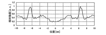
得られた発光装置について、長手方向の配光特性をシミュレーションした。その結果を図2Bに示す。
また、第1層を省略する以外、上記実施例の発光装置と実質的に同様の発光装置を形成し、同様に配光特性をシミュレーションした。
About the obtained light-emitting device, the light distribution characteristic of the longitudinal direction was simulated. The result is shown in FIG. 2B.
Further, a light emitting device substantially similar to the light emitting device of the above example was formed except that the first layer was omitted, and the light distribution characteristics were similarly simulated.
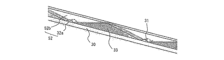
なお、比較例として、図3Aに示したように、透光性部材52の第2層52bにおいて、V字溝を有していない以外、上記実施例の発光装置と実質的に同様の発光装置を形成し、同様に配光特性をシミュレーションした。その結果を図3Bに示す。
As a comparative example, as shown in FIG. 3A, the
図2Bによれば、本実施例では、V字溝を配置することにより、発光素子間の正面がよりフラットに近い配光を得ることができた。
また、透光性部材が単層である場合においても、実質的に図2Bの配光と同様の配光を得ることができることがわかった。
一方、V字溝を有さない場合には、発光素子間の正面において極端に輝度が低く、発光素子上においては極端に輝度が高く、均一な配光を得ることができない。
According to FIG. 2B, in this example, by arranging the V-shaped grooves, it was possible to obtain a light distribution in which the front surface between the light emitting elements was more flat.
Further, it was found that even when the translucent member is a single layer, it is possible to obtain a light distribution substantially similar to the light distribution in FIG. 2B.
On the other hand, when there is no V-shaped groove, the luminance is extremely low in front of the light emitting elements, and the luminance is extremely high on the light emitting elements, so that uniform light distribution cannot be obtained.
このように、本発明の発光装置によれば、発光素子を用いて、特に、線状光源装置の場合においても、線状光源装置の中心部から端部にわたって光を広げる事が可能な発光装置を提供する事ができる。そして、複数個の発光素子を並べた場合においても、発光素子と発光素子の間まで発光素子からの光が届く発光装置を提供することができる。
また、発光装置を導光板と組み合わせた場合の装置全体の小型化及び簡素化を図りながら、所望の配光特性を実現することができ、導光板等の複雑な設計をより容易に実現することが可能となる。
As described above, according to the light-emitting device of the present invention, the light-emitting device can spread light from the center to the end of the linear light source device, particularly in the case of the linear light source device. Can be provided. Even when a plurality of light-emitting elements are arranged, a light-emitting device in which light from the light-emitting elements reaches between the light-emitting elements can be provided.
In addition, when the light emitting device is combined with the light guide plate, it is possible to achieve desired light distribution characteristics while reducing the size and simplification of the entire device, and to more easily realize a complicated design of the light guide plate and the like. Is possible.
本発明の発光装置は、照明器具、車両搭載用照明、ディスプレイ、インジケータ等のバックライトとして利用することができる。 The light-emitting device of the present invention can be used as a backlight for lighting fixtures, vehicle-mounted lighting, displays, indicators, and the like.
10、30 基板
11、31 発光素子
12、32、52、54 透光性部材
12a、32a 第1層
12b、32b、52b、54b 第2層
13、33 反射部材
22、42 溝部(V字溝)
10, 30
Claims (7)
該発光素子と前記一対の反射部材の少なくとも一部を被覆する透光性部材とを備えた発光装置であって、
前記透光性部材は、前記発光装置の側面において露出する第1の側面及び該第1の側面と対面する第2の側面を有しており、前記発光素子の上方に、第1の側面から第2の側面まで延伸する溝部を有することを特徴とする発光装置。 A substrate, a light emitting element placed on the substrate, a pair of reflecting members provided on the substrate so as to sandwich the light emitting element,
A light emitting device comprising the light emitting element and a translucent member covering at least a part of the pair of reflecting members,
The translucent member has a first side surface exposed on a side surface of the light emitting device and a second side surface facing the first side surface, and the first side surface is disposed above the light emitting element. A light-emitting device having a groove extending to the second side surface.
Priority Applications (1)
| Application Number | Priority Date | Filing Date | Title |
|---|---|---|---|
| JP2008186053A JP5309749B2 (en) | 2008-07-17 | 2008-07-17 | Light emitting device |
Applications Claiming Priority (1)
| Application Number | Priority Date | Filing Date | Title |
|---|---|---|---|
| JP2008186053A JP5309749B2 (en) | 2008-07-17 | 2008-07-17 | Light emitting device |
Publications (2)
| Publication Number | Publication Date |
|---|---|
| JP2010027782A true JP2010027782A (en) | 2010-02-04 |
| JP5309749B2 JP5309749B2 (en) | 2013-10-09 |
Family
ID=41733342
Family Applications (1)
| Application Number | Title | Priority Date | Filing Date |
|---|---|---|---|
| JP2008186053A Active JP5309749B2 (en) | 2008-07-17 | 2008-07-17 | Light emitting device |
Country Status (1)
| Country | Link |
|---|---|
| JP (1) | JP5309749B2 (en) |
Citations (4)
| Publication number | Priority date | Publication date | Assignee | Title |
|---|---|---|---|---|
| JP2004165124A (en) * | 2002-09-20 | 2004-06-10 | Sanyo Electric Co Ltd | Linear illumination device and surface illumination device using it |
| JP2007194161A (en) * | 2006-01-23 | 2007-08-02 | Matsushita Electric Ind Co Ltd | Linear light source device |
| JP3134119U (en) * | 2007-02-02 | 2007-08-02 | 凱鼎科技股▲ふん▼有限公司 | Light emitting diode |
| JP2008010691A (en) * | 2006-06-30 | 2008-01-17 | Hitachi Displays Ltd | Illuminator and display device employing illuminator |
-
2008
- 2008-07-17 JP JP2008186053A patent/JP5309749B2/en active Active
Patent Citations (4)
| Publication number | Priority date | Publication date | Assignee | Title |
|---|---|---|---|---|
| JP2004165124A (en) * | 2002-09-20 | 2004-06-10 | Sanyo Electric Co Ltd | Linear illumination device and surface illumination device using it |
| JP2007194161A (en) * | 2006-01-23 | 2007-08-02 | Matsushita Electric Ind Co Ltd | Linear light source device |
| JP2008010691A (en) * | 2006-06-30 | 2008-01-17 | Hitachi Displays Ltd | Illuminator and display device employing illuminator |
| JP3134119U (en) * | 2007-02-02 | 2007-08-02 | 凱鼎科技股▲ふん▼有限公司 | Light emitting diode |
Also Published As
| Publication number | Publication date |
|---|---|
| JP5309749B2 (en) | 2013-10-09 |
Similar Documents
| Publication | Publication Date | Title |
|---|---|---|
| US10971656B2 (en) | Resin molding, surface mounted light emitting apparatus and methods for manufacturing the same | |
| JP4953578B2 (en) | Light emitting device | |
| JP5123466B2 (en) | Light emitting device | |
| JP4956977B2 (en) | Light emitting device | |
| JP6519311B2 (en) | Light emitting device | |
| US10825968B2 (en) | Method for manufacturing light-emitting device | |
| JP5103831B2 (en) | Semiconductor manufacturing method | |
| KR101204115B1 (en) | Light emitting device with light distribution characteristic controlling lens | |
| JP4855869B2 (en) | Method for manufacturing light emitting device | |
| JP6079209B2 (en) | Light emitting device and manufacturing method thereof | |
| JP4622253B2 (en) | Light emitting device and manufacturing method thereof | |
| WO2010026716A1 (en) | Light emitting device, resin package, resin-molded body, and methods for manufacturing light emitting device, resin package and resin-molded body | |
| JP2007329219A (en) | Resin forming body, surface mount light-emitting device, and method of manufacturing these | |
| JP2006269778A (en) | Optical device | |
| JP4543712B2 (en) | Method for manufacturing light emitting device | |
| JP6523597B2 (en) | Light emitting device | |
| JP5755420B2 (en) | Light emitting device | |
| JP2008153553A (en) | Light-emitting device and method of manufacturing same | |
| JP2007234968A (en) | Light emitting device and manufacturing method of same | |
| JP4617761B2 (en) | Method for manufacturing light emitting device | |
| JP2006287032A (en) | Light emitting device | |
| JP5294741B2 (en) | RESIN MOLDED BODY, SURFACE MOUNTED LIGHT EMITTING DEVICE AND METHOD FOR PRODUCING THEM | |
| JP5309749B2 (en) | Light emitting device | |
| JP5205773B2 (en) | Light emitting device | |
| JP2016029732A (en) | Light-emitting device, resin package, resin mold and manufacturing methods thereof |
Legal Events
| Date | Code | Title | Description |
|---|---|---|---|
| A621 | Written request for application examination |
Free format text: JAPANESE INTERMEDIATE CODE: A621 Effective date: 20110620 |
|
| A131 | Notification of reasons for refusal |
Free format text: JAPANESE INTERMEDIATE CODE: A131 Effective date: 20120703 |
|
| A977 | Report on retrieval |
Free format text: JAPANESE INTERMEDIATE CODE: A971007 Effective date: 20120704 |
|
| A521 | Request for written amendment filed |
Free format text: JAPANESE INTERMEDIATE CODE: A523 Effective date: 20120831 |
|
| A131 | Notification of reasons for refusal |
Free format text: JAPANESE INTERMEDIATE CODE: A131 Effective date: 20121211 |
|
| A521 | Request for written amendment filed |
Free format text: JAPANESE INTERMEDIATE CODE: A523 Effective date: 20130207 |
|
| RD02 | Notification of acceptance of power of attorney |
Free format text: JAPANESE INTERMEDIATE CODE: A7422 Effective date: 20130207 |
|
| A131 | Notification of reasons for refusal |
Free format text: JAPANESE INTERMEDIATE CODE: A131 Effective date: 20130507 |
|
| A521 | Request for written amendment filed |
Free format text: JAPANESE INTERMEDIATE CODE: A523 Effective date: 20130507 |
|
| TRDD | Decision of grant or rejection written | ||
| A01 | Written decision to grant a patent or to grant a registration (utility model) |
Free format text: JAPANESE INTERMEDIATE CODE: A01 Effective date: 20130604 |
|
| A61 | First payment of annual fees (during grant procedure) |
Free format text: JAPANESE INTERMEDIATE CODE: A61 Effective date: 20130617 |
|
| R150 | Certificate of patent or registration of utility model |
Free format text: JAPANESE INTERMEDIATE CODE: R150 Ref document number: 5309749 Country of ref document: JP Free format text: JAPANESE INTERMEDIATE CODE: R150 |
|
| R250 | Receipt of annual fees |
Free format text: JAPANESE INTERMEDIATE CODE: R250 |
|
| R250 | Receipt of annual fees |
Free format text: JAPANESE INTERMEDIATE CODE: R250 |
|
| R250 | Receipt of annual fees |
Free format text: JAPANESE INTERMEDIATE CODE: R250 |
|
| R250 | Receipt of annual fees |
Free format text: JAPANESE INTERMEDIATE CODE: R250 |
|
| R250 | Receipt of annual fees |
Free format text: JAPANESE INTERMEDIATE CODE: R250 |
|
| R250 | Receipt of annual fees |
Free format text: JAPANESE INTERMEDIATE CODE: R250 |
|
| R250 | Receipt of annual fees |
Free format text: JAPANESE INTERMEDIATE CODE: R250 |