JP2010027591A - Organic electroluminescence display device, and manufacturing method of the same - Google Patents
Organic electroluminescence display device, and manufacturing method of the same Download PDFInfo
- Publication number
- JP2010027591A JP2010027591A JP2008317928A JP2008317928A JP2010027591A JP 2010027591 A JP2010027591 A JP 2010027591A JP 2008317928 A JP2008317928 A JP 2008317928A JP 2008317928 A JP2008317928 A JP 2008317928A JP 2010027591 A JP2010027591 A JP 2010027591A
- Authority
- JP
- Japan
- Prior art keywords
- sacrificial layer
- layer
- light emitting
- organic light
- connection electrode
- Prior art date
- Legal status (The legal status is an assumption and is not a legal conclusion. Google has not performed a legal analysis and makes no representation as to the accuracy of the status listed.)
- Granted
Links
- 238000004519 manufacturing process Methods 0.000 title claims abstract description 29
- 238000005401 electroluminescence Methods 0.000 title claims abstract 4
- 239000000758 substrate Substances 0.000 claims abstract description 53
- 238000000034 method Methods 0.000 claims description 44
- 238000005530 etching Methods 0.000 claims description 26
- 229920002120 photoresistant polymer Polymers 0.000 claims description 19
- 229910018503 SF6 Inorganic materials 0.000 claims description 18
- SFZCNBIFKDRMGX-UHFFFAOYSA-N sulfur hexafluoride Chemical compound FS(F)(F)(F)(F)F SFZCNBIFKDRMGX-UHFFFAOYSA-N 0.000 claims description 18
- 229960000909 sulfur hexafluoride Drugs 0.000 claims description 18
- QVGXLLKOCUKJST-UHFFFAOYSA-N atomic oxygen Chemical compound [O] QVGXLLKOCUKJST-UHFFFAOYSA-N 0.000 claims description 17
- 229910052760 oxygen Inorganic materials 0.000 claims description 17
- 239000001301 oxygen Substances 0.000 claims description 17
- 229910052751 metal Inorganic materials 0.000 claims description 13
- 239000002184 metal Substances 0.000 claims description 13
- 229910044991 metal oxide Inorganic materials 0.000 claims description 8
- 150000004706 metal oxides Chemical class 0.000 claims description 8
- 238000001312 dry etching Methods 0.000 claims description 4
- 239000010410 layer Substances 0.000 description 226
- 239000010408 film Substances 0.000 description 48
- 239000000463 material Substances 0.000 description 25
- ZOKXTWBITQBERF-UHFFFAOYSA-N Molybdenum Chemical compound [Mo] ZOKXTWBITQBERF-UHFFFAOYSA-N 0.000 description 20
- 239000011733 molybdenum Substances 0.000 description 20
- 229910052750 molybdenum Inorganic materials 0.000 description 20
- PXHVJJICTQNCMI-UHFFFAOYSA-N Nickel Chemical compound [Ni] PXHVJJICTQNCMI-UHFFFAOYSA-N 0.000 description 18
- VYPSYNLAJGMNEJ-UHFFFAOYSA-N Silicium dioxide Chemical compound O=[Si]=O VYPSYNLAJGMNEJ-UHFFFAOYSA-N 0.000 description 16
- 238000002347 injection Methods 0.000 description 16
- 239000007924 injection Substances 0.000 description 16
- 229910052814 silicon oxide Inorganic materials 0.000 description 16
- 229910052782 aluminium Inorganic materials 0.000 description 14
- XAGFODPZIPBFFR-UHFFFAOYSA-N aluminium Chemical compound [Al] XAGFODPZIPBFFR-UHFFFAOYSA-N 0.000 description 14
- 239000011651 chromium Substances 0.000 description 12
- 239000010949 copper Substances 0.000 description 12
- 239000010931 gold Substances 0.000 description 12
- 239000010936 titanium Substances 0.000 description 12
- 229910052581 Si3N4 Inorganic materials 0.000 description 8
- 230000000694 effects Effects 0.000 description 8
- HQVNEWCFYHHQES-UHFFFAOYSA-N silicon nitride Chemical compound N12[Si]34N5[Si]62N3[Si]51N64 HQVNEWCFYHHQES-UHFFFAOYSA-N 0.000 description 8
- 239000011368 organic material Substances 0.000 description 7
- VYZAMTAEIAYCRO-UHFFFAOYSA-N Chromium Chemical compound [Cr] VYZAMTAEIAYCRO-UHFFFAOYSA-N 0.000 description 6
- RYGMFSIKBFXOCR-UHFFFAOYSA-N Copper Chemical compound [Cu] RYGMFSIKBFXOCR-UHFFFAOYSA-N 0.000 description 6
- 229910052779 Neodymium Inorganic materials 0.000 description 6
- RTAQQCXQSZGOHL-UHFFFAOYSA-N Titanium Chemical compound [Ti] RTAQQCXQSZGOHL-UHFFFAOYSA-N 0.000 description 6
- 229910045601 alloy Inorganic materials 0.000 description 6
- 239000000956 alloy Substances 0.000 description 6
- UBSJOWMHLJZVDJ-UHFFFAOYSA-N aluminum neodymium Chemical compound [Al].[Nd] UBSJOWMHLJZVDJ-UHFFFAOYSA-N 0.000 description 6
- 229910052804 chromium Inorganic materials 0.000 description 6
- 229910052802 copper Inorganic materials 0.000 description 6
- PCHJSUWPFVWCPO-UHFFFAOYSA-N gold Chemical compound [Au] PCHJSUWPFVWCPO-UHFFFAOYSA-N 0.000 description 6
- 229910052737 gold Inorganic materials 0.000 description 6
- QEFYFXOXNSNQGX-UHFFFAOYSA-N neodymium atom Chemical compound [Nd] QEFYFXOXNSNQGX-UHFFFAOYSA-N 0.000 description 6
- 229910052759 nickel Inorganic materials 0.000 description 6
- 239000011347 resin Substances 0.000 description 6
- 229920005989 resin Polymers 0.000 description 6
- 229910052719 titanium Inorganic materials 0.000 description 6
- 230000005525 hole transport Effects 0.000 description 5
- 239000011159 matrix material Substances 0.000 description 5
- 229920001721 polyimide Polymers 0.000 description 5
- 229910000838 Al alloy Inorganic materials 0.000 description 4
- OAICVXFJPJFONN-UHFFFAOYSA-N Phosphorus Chemical compound [P] OAICVXFJPJFONN-UHFFFAOYSA-N 0.000 description 4
- 229910021417 amorphous silicon Inorganic materials 0.000 description 4
- UMIVXZPTRXBADB-UHFFFAOYSA-N benzocyclobutene Chemical compound C1=CC=C2CCC2=C1 UMIVXZPTRXBADB-UHFFFAOYSA-N 0.000 description 4
- 230000003647 oxidation Effects 0.000 description 4
- 238000007254 oxidation reaction Methods 0.000 description 4
- 239000002356 single layer Substances 0.000 description 4
- 239000012780 transparent material Substances 0.000 description 4
- 239000004925 Acrylic resin Substances 0.000 description 3
- 229920000178 Acrylic resin Polymers 0.000 description 3
- 239000002019 doping agent Substances 0.000 description 3
- 238000010943 off-gassing Methods 0.000 description 3
- 239000009719 polyimide resin Substances 0.000 description 3
- TVIVIEFSHFOWTE-UHFFFAOYSA-K tri(quinolin-8-yloxy)alumane Chemical compound [Al+3].C1=CN=C2C([O-])=CC=CC2=C1.C1=CN=C2C([O-])=CC=CC2=C1.C1=CN=C2C([O-])=CC=CC2=C1 TVIVIEFSHFOWTE-UHFFFAOYSA-K 0.000 description 3
- POILWHVDKZOXJZ-ARJAWSKDSA-M (z)-4-oxopent-2-en-2-olate Chemical compound C\C([O-])=C\C(C)=O POILWHVDKZOXJZ-ARJAWSKDSA-M 0.000 description 2
- 229920001609 Poly(3,4-ethylenedioxythiophene) Polymers 0.000 description 2
- 239000004642 Polyimide Substances 0.000 description 2
- CUJRVFIICFDLGR-UHFFFAOYSA-N acetylacetonate Chemical compound CC(=O)[CH-]C(C)=O CUJRVFIICFDLGR-UHFFFAOYSA-N 0.000 description 2
- 239000000853 adhesive Substances 0.000 description 2
- 230000001070 adhesive effect Effects 0.000 description 2
- UFVXQDWNSAGPHN-UHFFFAOYSA-K bis[(2-methylquinolin-8-yl)oxy]-(4-phenylphenoxy)alumane Chemical compound [Al+3].C1=CC=C([O-])C2=NC(C)=CC=C21.C1=CC=C([O-])C2=NC(C)=CC=C21.C1=CC([O-])=CC=C1C1=CC=CC=C1 UFVXQDWNSAGPHN-UHFFFAOYSA-K 0.000 description 2
- 238000010586 diagram Methods 0.000 description 2
- 239000012535 impurity Substances 0.000 description 2
- 229910052741 iridium Inorganic materials 0.000 description 2
- GKOZUEZYRPOHIO-UHFFFAOYSA-N iridium atom Chemical compound [Ir] GKOZUEZYRPOHIO-UHFFFAOYSA-N 0.000 description 2
- UEEXRMUCXBPYOV-UHFFFAOYSA-N iridium;2-phenylpyridine Chemical compound [Ir].C1=CC=CC=C1C1=CC=CC=N1.C1=CC=CC=C1C1=CC=CC=N1.C1=CC=CC=C1C1=CC=CC=N1 UEEXRMUCXBPYOV-UHFFFAOYSA-N 0.000 description 2
- 238000002161 passivation Methods 0.000 description 2
- 229920000767 polyaniline Polymers 0.000 description 2
- 229910021420 polycrystalline silicon Inorganic materials 0.000 description 2
- 229920000642 polymer Polymers 0.000 description 2
- 239000010409 thin film Substances 0.000 description 2
- ZSYMVHGRKPBJCQ-UHFFFAOYSA-N 1,1'-biphenyl;9h-carbazole Chemical group C1=CC=CC=C1C1=CC=CC=C1.C1=CC=C2C3=CC=CC=C3NC2=C1 ZSYMVHGRKPBJCQ-UHFFFAOYSA-N 0.000 description 1
- VBQVHWHWZOUENI-UHFFFAOYSA-N 1-phenyl-2H-quinoline Chemical compound C1C=CC2=CC=CC=C2N1C1=CC=CC=C1 VBQVHWHWZOUENI-UHFFFAOYSA-N 0.000 description 1
- LPCWDYWZIWDTCV-UHFFFAOYSA-N 1-phenylisoquinoline Chemical compound C1=CC=CC=C1C1=NC=CC2=CC=CC=C12 LPCWDYWZIWDTCV-UHFFFAOYSA-N 0.000 description 1
- VFMUXPQZKOKPOF-UHFFFAOYSA-N 2,3,7,8,12,13,17,18-octaethyl-21,23-dihydroporphyrin platinum Chemical compound [Pt].CCc1c(CC)c2cc3[nH]c(cc4nc(cc5[nH]c(cc1n2)c(CC)c5CC)c(CC)c4CC)c(CC)c3CC VFMUXPQZKOKPOF-UHFFFAOYSA-N 0.000 description 1
- HONWGFNQCPRRFM-UHFFFAOYSA-N 2-n-(3-methylphenyl)-1-n,1-n,2-n-triphenylbenzene-1,2-diamine Chemical compound CC1=CC=CC(N(C=2C=CC=CC=2)C=2C(=CC=CC=2)N(C=2C=CC=CC=2)C=2C=CC=CC=2)=C1 HONWGFNQCPRRFM-UHFFFAOYSA-N 0.000 description 1
- YCKRFDGAMUMZLT-UHFFFAOYSA-N Fluorine atom Chemical compound [F] YCKRFDGAMUMZLT-UHFFFAOYSA-N 0.000 description 1
- YNPNZTXNASCQKK-UHFFFAOYSA-N Phenanthrene Natural products C1=CC=C2C3=CC=CC=C3C=CC2=C1 YNPNZTXNASCQKK-UHFFFAOYSA-N 0.000 description 1
- XUIMIQQOPSSXEZ-UHFFFAOYSA-N Silicon Chemical compound [Si] XUIMIQQOPSSXEZ-UHFFFAOYSA-N 0.000 description 1
- 239000007983 Tris buffer Substances 0.000 description 1
- BZHJMEDXRYGGRV-UHFFFAOYSA-N Vinyl chloride Chemical compound ClC=C BZHJMEDXRYGGRV-UHFFFAOYSA-N 0.000 description 1
- DGEZNRSVGBDHLK-UHFFFAOYSA-N [1,10]phenanthroline Chemical compound C1=CN=C2C3=NC=CC=C3C=CC2=C1 DGEZNRSVGBDHLK-UHFFFAOYSA-N 0.000 description 1
- PJRJXFPRMUZBHQ-UHFFFAOYSA-N [Ir].C1C=CC2=CC=CC=C2N1C1=CC=CC=C1.C1C=CC2=CC=CC=C2N1C1=CC=CC=C1.C1C=CC2=CC=CC=C2N1C1=CC=CC=C1 Chemical compound [Ir].C1C=CC2=CC=CC=C2N1C1=CC=CC=C1.C1C=CC2=CC=CC=C2N1C1=CC=CC=C1.C1C=CC2=CC=CC=C2N1C1=CC=CC=C1 PJRJXFPRMUZBHQ-UHFFFAOYSA-N 0.000 description 1
- 125000004556 carbazol-9-yl group Chemical group C1=CC=CC=2C3=CC=CC=C3N(C12)* 0.000 description 1
- 239000000919 ceramic Substances 0.000 description 1
- XCJYREBRNVKWGJ-UHFFFAOYSA-N copper(II) phthalocyanine Chemical compound [Cu+2].C12=CC=CC=C2C(N=C2[N-]C(C3=CC=CC=C32)=N2)=NC1=NC([C]1C=CC=CC1=1)=NC=1N=C1[C]3C=CC=CC3=C2[N-]1 XCJYREBRNVKWGJ-UHFFFAOYSA-N 0.000 description 1
- 230000005684 electric field Effects 0.000 description 1
- 239000003822 epoxy resin Substances 0.000 description 1
- 239000011737 fluorine Substances 0.000 description 1
- 229910052731 fluorine Inorganic materials 0.000 description 1
- 239000011521 glass Substances 0.000 description 1
- 238000000059 patterning Methods 0.000 description 1
- 125000002080 perylenyl group Chemical group C1(=CC=C2C=CC=C3C4=CC=CC5=CC=CC(C1=C23)=C45)* 0.000 description 1
- CSHWQDPOILHKBI-UHFFFAOYSA-N peryrene Natural products C1=CC(C2=CC=CC=3C2=C2C=CC=3)=C3C2=CC=CC3=C1 CSHWQDPOILHKBI-UHFFFAOYSA-N 0.000 description 1
- IEQIEDJGQAUEQZ-UHFFFAOYSA-N phthalocyanine Chemical compound N1C(N=C2C3=CC=CC=C3C(N=C3C4=CC=CC=C4C(=N4)N3)=N2)=C(C=CC=C2)C2=C1N=C1C2=CC=CC=C2C4=N1 IEQIEDJGQAUEQZ-UHFFFAOYSA-N 0.000 description 1
- 239000004033 plastic Substances 0.000 description 1
- 229920003023 plastic Polymers 0.000 description 1
- 229920005668 polycarbonate resin Polymers 0.000 description 1
- 239000004431 polycarbonate resin Substances 0.000 description 1
- 229920000647 polyepoxide Polymers 0.000 description 1
- 229920001225 polyester resin Polymers 0.000 description 1
- 239000004645 polyester resin Substances 0.000 description 1
- -1 polyethylene terephthalate Polymers 0.000 description 1
- 229920000139 polyethylene terephthalate Polymers 0.000 description 1
- 239000005020 polyethylene terephthalate Substances 0.000 description 1
- 229910052710 silicon Inorganic materials 0.000 description 1
- 239000010703 silicon Substances 0.000 description 1
- 239000000126 substance Substances 0.000 description 1
- 238000001039 wet etching Methods 0.000 description 1
Images


Classifications
-
- H—ELECTRICITY
- H10—SEMICONDUCTOR DEVICES; ELECTRIC SOLID-STATE DEVICES NOT OTHERWISE PROVIDED FOR
- H10K—ORGANIC ELECTRIC SOLID-STATE DEVICES
- H10K59/00—Integrated devices, or assemblies of multiple devices, comprising at least one organic light-emitting element covered by group H10K50/00
- H10K59/10—OLED displays
- H10K59/12—Active-matrix OLED [AMOLED] displays
- H10K59/122—Pixel-defining structures or layers, e.g. banks
-
- H—ELECTRICITY
- H01—ELECTRIC ELEMENTS
- H01L—SEMICONDUCTOR DEVICES NOT COVERED BY CLASS H10
- H01L21/00—Processes or apparatus adapted for the manufacture or treatment of semiconductor or solid state devices or of parts thereof
- H01L21/02—Manufacture or treatment of semiconductor devices or of parts thereof
- H01L21/04—Manufacture or treatment of semiconductor devices or of parts thereof the devices having at least one potential-jump barrier or surface barrier, e.g. PN junction, depletion layer or carrier concentration layer
- H01L21/18—Manufacture or treatment of semiconductor devices or of parts thereof the devices having at least one potential-jump barrier or surface barrier, e.g. PN junction, depletion layer or carrier concentration layer the devices having semiconductor bodies comprising elements of Group IV of the Periodic System or AIIIBV compounds with or without impurities, e.g. doping materials
- H01L21/30—Treatment of semiconductor bodies using processes or apparatus not provided for in groups H01L21/20 - H01L21/26
- H01L21/31—Treatment of semiconductor bodies using processes or apparatus not provided for in groups H01L21/20 - H01L21/26 to form insulating layers thereon, e.g. for masking or by using photolithographic techniques; After treatment of these layers; Selection of materials for these layers
- H01L21/3105—After-treatment
- H01L21/31051—Planarisation of the insulating layers
- H01L21/31053—Planarisation of the insulating layers involving a dielectric removal step
- H01L21/31055—Planarisation of the insulating layers involving a dielectric removal step the removal being a chemical etching step, e.g. dry etching
-
- H—ELECTRICITY
- H10—SEMICONDUCTOR DEVICES; ELECTRIC SOLID-STATE DEVICES NOT OTHERWISE PROVIDED FOR
- H10K—ORGANIC ELECTRIC SOLID-STATE DEVICES
- H10K10/00—Organic devices specially adapted for rectifying, amplifying, oscillating or switching; Organic capacitors or resistors having a potential-jump barrier or a surface barrier
- H10K10/80—Constructional details
- H10K10/82—Electrodes
- H10K10/84—Ohmic electrodes, e.g. source or drain electrodes
-
- H—ELECTRICITY
- H10—SEMICONDUCTOR DEVICES; ELECTRIC SOLID-STATE DEVICES NOT OTHERWISE PROVIDED FOR
- H10K—ORGANIC ELECTRIC SOLID-STATE DEVICES
- H10K50/00—Organic light-emitting devices
- H10K50/10—OLEDs or polymer light-emitting diodes [PLED]
- H10K50/14—Carrier transporting layers
- H10K50/15—Hole transporting layers
-
- H—ELECTRICITY
- H10—SEMICONDUCTOR DEVICES; ELECTRIC SOLID-STATE DEVICES NOT OTHERWISE PROVIDED FOR
- H10K—ORGANIC ELECTRIC SOLID-STATE DEVICES
- H10K50/00—Organic light-emitting devices
- H10K50/10—OLEDs or polymer light-emitting diodes [PLED]
- H10K50/14—Carrier transporting layers
- H10K50/16—Electron transporting layers
-
- H—ELECTRICITY
- H10—SEMICONDUCTOR DEVICES; ELECTRIC SOLID-STATE DEVICES NOT OTHERWISE PROVIDED FOR
- H10K—ORGANIC ELECTRIC SOLID-STATE DEVICES
- H10K50/00—Organic light-emitting devices
- H10K50/10—OLEDs or polymer light-emitting diodes [PLED]
- H10K50/17—Carrier injection layers
- H10K50/171—Electron injection layers
-
- H—ELECTRICITY
- H10—SEMICONDUCTOR DEVICES; ELECTRIC SOLID-STATE DEVICES NOT OTHERWISE PROVIDED FOR
- H10K—ORGANIC ELECTRIC SOLID-STATE DEVICES
- H10K59/00—Integrated devices, or assemblies of multiple devices, comprising at least one organic light-emitting element covered by group H10K50/00
- H10K59/10—OLED displays
- H10K59/12—Active-matrix OLED [AMOLED] displays
- H10K59/123—Connection of the pixel electrodes to the thin film transistors [TFT]
-
- H—ELECTRICITY
- H10—SEMICONDUCTOR DEVICES; ELECTRIC SOLID-STATE DEVICES NOT OTHERWISE PROVIDED FOR
- H10K—ORGANIC ELECTRIC SOLID-STATE DEVICES
- H10K77/00—Constructional details of devices covered by this subclass and not covered by groups H10K10/80, H10K30/80, H10K50/80 or H10K59/80
- H10K77/10—Substrates, e.g. flexible substrates
-
- H—ELECTRICITY
- H01—ELECTRIC ELEMENTS
- H01L—SEMICONDUCTOR DEVICES NOT COVERED BY CLASS H10
- H01L2224/00—Indexing scheme for arrangements for connecting or disconnecting semiconductor or solid-state bodies and methods related thereto as covered by H01L24/00
- H01L2224/01—Means for bonding being attached to, or being formed on, the surface to be connected, e.g. chip-to-package, die-attach, "first-level" interconnects; Manufacturing methods related thereto
- H01L2224/02—Bonding areas; Manufacturing methods related thereto
- H01L2224/03—Manufacturing methods
- H01L2224/03001—Involving a temporary auxiliary member not forming part of the manufacturing apparatus, e.g. removable or sacrificial coating, film or substrate
-
- Y—GENERAL TAGGING OF NEW TECHNOLOGICAL DEVELOPMENTS; GENERAL TAGGING OF CROSS-SECTIONAL TECHNOLOGIES SPANNING OVER SEVERAL SECTIONS OF THE IPC; TECHNICAL SUBJECTS COVERED BY FORMER USPC CROSS-REFERENCE ART COLLECTIONS [XRACs] AND DIGESTS
- Y02—TECHNOLOGIES OR APPLICATIONS FOR MITIGATION OR ADAPTATION AGAINST CLIMATE CHANGE
- Y02E—REDUCTION OF GREENHOUSE GAS [GHG] EMISSIONS, RELATED TO ENERGY GENERATION, TRANSMISSION OR DISTRIBUTION
- Y02E10/00—Energy generation through renewable energy sources
- Y02E10/50—Photovoltaic [PV] energy
- Y02E10/549—Organic PV cells
-
- Y—GENERAL TAGGING OF NEW TECHNOLOGICAL DEVELOPMENTS; GENERAL TAGGING OF CROSS-SECTIONAL TECHNOLOGIES SPANNING OVER SEVERAL SECTIONS OF THE IPC; TECHNICAL SUBJECTS COVERED BY FORMER USPC CROSS-REFERENCE ART COLLECTIONS [XRACs] AND DIGESTS
- Y02—TECHNOLOGIES OR APPLICATIONS FOR MITIGATION OR ADAPTATION AGAINST CLIMATE CHANGE
- Y02P—CLIMATE CHANGE MITIGATION TECHNOLOGIES IN THE PRODUCTION OR PROCESSING OF GOODS
- Y02P70/00—Climate change mitigation technologies in the production process for final industrial or consumer products
- Y02P70/50—Manufacturing or production processes characterised by the final manufactured product
Abstract
Description
本発明は、有機電界発光表示装置及びその製造方法に関するものである。 The present invention relates to an organic light emitting display device and a method for manufacturing the same.
有機電界発光表示装置に使われる有機電界発光素子は、基板上に位置する2つの電極間に発光層が形成された自発光素子である。
また、有機電界発光表示装置は、光が放出される方向によって、前面発光方式、背面発光方式、または両面発光方式などがある。そして、駆動方式によって手動マトリックス型(Passive Matrix)と能動マトリックス型(Active Matrix)とに分けられる。
An organic light emitting device used in an organic light emitting display device is a self light emitting device in which a light emitting layer is formed between two electrodes located on a substrate.
In addition, the organic light emitting display device has a front light emission method, a back light emission method, a double light emission method, or the like depending on a direction in which light is emitted. And, it can be divided into a manual matrix type (Passive Matrix) and an active matrix type (Active Matrix) according to the driving method.
このような有機電界発光表示装置は、マトリックス形態で配置された複数のサブピクセルに、スキャン信号、データ信号、及び電源などが供給されると、選択されたサブピクセルが発光することによって映像を表示することができる。 Such an organic light emitting display device displays an image by emitting light from a selected sub-pixel when a scan signal, a data signal, and a power source are supplied to a plurality of sub-pixels arranged in a matrix form. can do.
一方、従来の有機電界発光表示装置は、ゲート、ソース、及びドレインを含むトランジスタ上にソースまたはドレインに連結されるカソードを形成し、チャンバーを移動して有機発光層とアノードを形成する工程を経る。 Meanwhile, a conventional organic light emitting display device includes a step of forming a cathode connected to a source or drain on a transistor including a gate, a source, and a drain, and moving the chamber to form an organic light emitting layer and an anode. .
このような製造方法により形成された有機電界発光表示装置は、薄膜の構造または製造方法の手続きなどによりカソードが酸化されるにつれて、電子注入特性が低下する問題があった。そして、従来の有機電界発光表示装置は、カソード形成時にカソード間のショットや薄膜段差によるアノードオープン(切れ)のような問題がある。 The organic light emitting display device formed by such a manufacturing method has a problem that the electron injection characteristic is lowered as the cathode is oxidized by the structure of the thin film or the procedure of the manufacturing method. The conventional organic light emitting display has problems such as shots between the cathodes and anode open (cut) due to a thin film step when the cathodes are formed.
本発明の実施形態は、基板と、基板上に位置し、ゲート、ソース、及びドレインを含むトランジスタと、トランジスタ上に位置し、ソースまたはドレインに連結された連結電極と、連結電極上に位置し、連結電極の一部を露出する第1犠牲層と、第1犠牲層上に位置し、連結電極の一部を露出する第2犠牲層と、連結電極と第2犠牲層上に位置する下部電極と、下部電極上に位置する有機発光層と、有機発光層上に位置する上部電極とを含み、第1犠牲層が第2犠牲層より内側に引き込まれていることを特徴とする有機電界発光表示装置を提供する。 An embodiment of the present invention includes a substrate, a transistor positioned on the substrate and including a gate, a source, and a drain, a connection electrode positioned on the transistor and connected to the source or drain, and positioned on the connection electrode. A first sacrificial layer exposing a part of the connection electrode; a second sacrificial layer located on the first sacrificial layer; and a lower part located on the connection electrode and the second sacrificial layer. An organic electric field comprising: an electrode; an organic light emitting layer positioned on the lower electrode; and an upper electrode positioned on the organic light emitting layer, wherein the first sacrificial layer is drawn inward from the second sacrificial layer A light-emitting display device is provided.
本発明の他の態様によると、基板と、基板上に位置し、ゲート、ソース、及びドレインを含むトランジスタと、トランジスタ上に位置し、ソースまたはドレインに連結された連結電極と、連結電極上に位置し、連結電極の一部を露出する犠牲層と、犠牲層上に位置し、連結電極の一部を露出するバンク層と、連結電極とバンク層上に位置する下部電極と、下部電極上に位置する有機発光層と、有機発光層上に位置する上部電極とを含み、犠牲層がバンク層より内側に引き込まれていることを特徴とする有機電界発光表示装置を提供する。 According to another aspect of the present invention, a substrate, a transistor positioned on the substrate and including a gate, a source, and a drain, a connection electrode positioned on the transistor and connected to the source or drain, and on the connection electrode A sacrificial layer located on the sacrificial layer and exposing a part of the connecting electrode; a bank layer exposing a part of the connecting electrode; a lower electrode located on the connecting electrode and the bank layer; And an upper electrode located on the organic light emitting layer, and a sacrificial layer is drawn inward from the bank layer.
本発明の他の態様によると、基板上に、ゲート、ソース、及びドレインを含むトランジスタを形成するステップと、トランジスタ上にソースまたはドレインに連結される連結電極を形成するステップと、連結電極上に第1犠牲層を形成するステップと、第1犠牲層上に第2犠牲層を形成するステップと、第2犠牲層上に第2犠牲層の一部が露出されるようにフォトレジスタを形成するステップと、フォトレジスタの下部に第2犠牲層が引き込まれるように第1エッチング方法を用いて第2犠牲層を除去するステップと、第2犠牲層の下部に第1犠牲層が引き込まれるように第2エッチング方法を用いて第1犠牲層を除去するステップと、フォトレジスタを除去するステップと、連結電極上に下部電極を形成するステップと、下部電極上に有機発光層を形成するステップと、有機発光層上に上部電極を形成するステップと、を含む有機電界発光表示装置の製造方法を提供する。 According to another aspect of the present invention, forming a transistor including a gate, a source, and a drain on a substrate, forming a connection electrode connected to the source or drain on the transistor, and on the connection electrode Forming a first sacrificial layer; forming a second sacrificial layer on the first sacrificial layer; and forming a photoresist so that a portion of the second sacrificial layer is exposed on the second sacrificial layer. Removing the second sacrificial layer using a first etching method so that the second sacrificial layer is drawn under the photoresist; and pulling the first sacrificial layer under the second sacrificial layer. Removing the first sacrificial layer using the second etching method; removing the photoresist; forming a lower electrode on the connection electrode; and organic on the lower electrode Providing a step of forming a light layer, and forming an upper electrode on the organic emission layer, a method of manufacturing an organic light emitting display device including a.
本発明の他の態様によると、基板上に、ゲート、ソース、及びドレインを含むトランジスタを形成するステップと、トランジスタ上にソースまたはドレインに連結される連結電極を形成するステップと、連結電極上に犠牲層を形成するステップと、犠牲層上に犠牲層の一部が露出されるようにバンク層を形成するステップと、バンク層の下部に犠牲層が引き込まれるようにエッチング方法を用いて犠牲層を除去するステップと、連結電極上に下部電極を形成するステップと、下部電極上に有機発光層を形成するステップと、有機発光層上に上部電極を形成するステップとを含む有機電界発光表示装置の製造方法を提供する。 According to another aspect of the present invention, forming a transistor including a gate, a source, and a drain on a substrate, forming a connection electrode connected to the source or drain on the transistor, and on the connection electrode Forming a sacrificial layer; forming a bank layer so that a portion of the sacrificial layer is exposed on the sacrificial layer; and etching the sacrificial layer using an etching method so that the sacrificial layer is drawn below the bank layer An organic light emitting display comprising: a step of forming a lower electrode on the connection electrode; a step of forming an organic light emitting layer on the lower electrode; and a step of forming an upper electrode on the organic light emitting layer. A manufacturing method is provided.
本発明によると、アンダーカットによる段差により上部電極がオープン(切れ)される問題を抑制することができる。 According to the present invention, it is possible to suppress the problem that the upper electrode is opened (cut) due to a step due to undercut.
また、この場合、アンダーカットパターン時に使われる犠牲層の厚みが最小化できることは勿論、パターンされる深さも任意に調節できる効果がある。 In this case, the sacrificial layer used in the undercut pattern can be minimized in thickness, and the pattern depth can be adjusted arbitrarily.
また、アンダーカットパターンを用いて下部電極を形成し、有機発光層及び上部電極を形成するので、下部電極が酸化される問題を抑制できる効果がある。 In addition, since the lower electrode is formed using the undercut pattern and the organic light emitting layer and the upper electrode are formed, there is an effect that the problem of the lower electrode being oxidized can be suppressed.
また、下部電極の酸化を抑制できるので、電子注入特性を向上させることができることは勿論、発光効率も向上させることができる効果がある。 Further, since the oxidation of the lower electrode can be suppressed, the electron injection characteristics can be improved, and the light emission efficiency can be improved.
また、犠牲層の材料に無機絶縁膜を使用するので、犠牲層の下部に位置する有機材料によるアウト−ガッシング(out-gassing)影響(例えば、サブピクセル収縮)を最小化することができる効果が得られる。 In addition, since an inorganic insulating film is used as the material of the sacrificial layer, an effect of minimizing an out-gassing influence (for example, sub-pixel shrinkage) due to an organic material located below the sacrificial layer is achieved. can get.
以下、本発明の実施形態に係る具体的な実施形態を添付された図面を参照しつつ説明する。 Hereinafter, specific embodiments according to embodiments of the present invention will be described with reference to the accompanying drawings.
(第1実施形態)
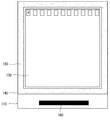
図1に示すように、有機電界発光表示装置は、基板110上に多数のサブピクセルPが位置する表示部130を含むことができる。
(First Embodiment)
As shown in FIG. 1, the organic light emitting display device may include a
基板110は、素子を形成するための材料に機械的強度や寸法安定性が優れるものを選択することができる。基板110の材料には、ガラス板、金属板、セラミック板、またはプラスチック板(ポリカーボネイト樹脂、アクリル樹脂、塩化ビニール樹脂、ポリエチレンテレフタレート樹脂、ポリイミド樹脂、ポリエステル樹脂、エポキシ樹脂、シリコン樹脂、ふっ素樹脂等)等を例に挙げることができる。
As the
サブピクセルPは、基板110上に位置するトランジスタとトランジスタ上に位置する有機発光ダイオードを含むことができる。
The subpixel P may include a transistor located on the
基板110上に位置する多数のサブピクセルPは、水分や酸素に脆弱である。これによって、封入基板140を具備し、表示部130の外郭基板110に接着部材150を形成して、基板110と封入基板140とを封止することができる。
Many subpixels P located on the
多数のサブピクセルPは、基板110上に位置する駆動部160により駆動されて映像を表現することができる。駆動部160は、外部から供給された各種信号に対応してスキャン信号及びデータ信号などを生成することができ、生成された信号などを表示部130に位置する多数のサブピクセルPに供給することができる。
The plurality of subpixels P can be driven by a
駆動部160は、多数のサブピクセルPにスキャン信号を供給するスキャン駆動部と、多数のサブピクセルPにデータ信号を供給するデータ駆動部とを含むことができる。ここで、駆動部160は、スキャン駆動部及びデータ駆動部が1つのチップに形成されたことを一例として概略的に図示したものであり、スキャン駆動部とデータ駆動部のうちの1つ以上は、基板110または基板110の外部に区分されて位置できる。
The
以下、図2を参照して本発明の実施形態に係るサブピクセルについてより詳細に説明する。 Hereinafter, the sub-pixel according to the embodiment of the present invention will be described in more detail with reference to FIG.
図2を参照すると、基板110上には、ゲート112a、112bが位置できる。ゲート112a、112bは、モリブデン(Mo)、アルミニウム(Al)、クロム(Cr)、金(Au)、チタニウム(Ti)、ニッケル(Ni)、ネオジム(Nd)、及び銅(Cu)からなる群から選択されるいずれか1つ、またはいずれか2つ以上からなる合金からなることができる。また、ゲート112a、112bは、モリブデン(Mo)、アルミニウム(Al)、クロム(Cr)、金(Au)、チタニウム(Ti)、ニッケル(Ni)、ネオジム(Nd)、及び銅(Cu)からなる群から選択されるいずれか1つ、またはいずれか2つ以上からなる合金からなる多重層であることができる。また、ゲート112a、112bは、モリブデン/アルミニウム−ネオジム、またはモリブデン/アルミニウムの2重層であることができる。
Referring to FIG. 2,
ゲート112a、112b上には、第1絶縁膜113が位置できる。第1絶縁膜113は、シリコン酸化物(SiOx)、シリコン窒化物(SiNx)、またはこれらの多重層であることができるが、これに限定されるのではない。
A first
第1絶縁膜113上にはアクティブ層114a、114bが位置できる。アクティブ層114a、114bは、非晶質シリコン、またはこれを結晶化した多結晶シリコンを含むことができる。ここで、図示してはいないが、アクティブ層114a、114bは、チャネル領域、ソース領域、及びドレイン領域を含むことができ、ソース領域及びドレイン領域には、P型またはN型不純物がドーピングされることができる。また、アクティブ層114a、114bは、接触抵抗を低めるためのオーミックコンタクト層を含むことができる。
アクティブ層114a、114b上には、ソース115a、115c及びドレイン115b、115dが位置できる。ソース115a、115c及びドレイン115b、115dは、単一層または多重層からなることができ、ソース115a、115c及びドレイン115b、115dが単一層の場合には、モリブデン(Mo)、アルミニウム(Al)、クロム(Cr)、金(Au)、チタニウム(Ti)、ニッケル(Ni)、ネオジム(Nd)、及び銅(Cu)からなる群から選択されるいずれか1つ、またはいずれか2つ以上からなる合金からなることができる。また、ソース115a、115c及びドレイン115b、115dが多重層の場合には、モリブデン/アルミニウム−ネオジムの2重層、モリブデン/アルミニウム/モリブデン、またはモリブデン/アルミニウム−ネオジム/モリブデンの3重層からなることができる。
ソース115a、115c及びドレイン115b、115d上には、第2絶縁膜116aが位置できる。第2絶縁膜116aは、シリコン酸化物(SiOx)、シリコン窒化物(SiNx)、またはこれらの多重層であることができるが、これに限定されるのではない。第2絶縁膜116aはパッシベーション膜であることができる。
A second
基板110上に位置するトランジスタのうち、ゲート112a、ソース115a及びドレイン115bは駆動トランジスタであり、ゲート112b、ソース115c及びドレイン115dはスイッチングトランジスタであることができる。駆動トランジスタのソース115a及びドレイン115bのうちの1つは、第2絶縁膜116a上に位置するシールド金属118aに連結されることができる。そして、駆動トランジスタのソース115aまたはドレイン115bのうちの1つは、スイッチングトランジスタのソース115c、またはドレイン115dに連結されることができる。
Of the transistors located on the
第2絶縁膜116a上には平坦度を高めるための第3絶縁膜116bが位置できる。第3絶縁膜116bは、ポリイミドなどの有機物を含むことができる。
A third
以上、基板110上に形成されたトランジスタがボトムゲート型であることを一例として説明した。しかしながら、基板110上に形成されるトランジスタは、ボトムゲート型だけでなく、トップゲート型でも形成されることができる。
As described above, the example in which the transistor formed over the
トランジスタの第3絶縁膜116b上には駆動トランジスタのソース115aまたはドレイン115bに連結された連結電極117が位置できる。
A
連結電極117上には連結電極117の一部を露出する第1犠牲層120が位置できる。第1犠牲層120は、シリコン酸化物(SiOx)、シリコン窒化物(SiNx)のような無機絶縁膜を含むことができる。
A first
第1犠牲層120上には連結電極117の一部を露出する第2犠牲層121が位置できる。第2犠牲層121は、金属または金属酸化物を含むことができる。第2犠牲層121の材料に金属または金属酸化物を用いると、アンダーカットパターン時に助けを与えるだけでなく、下部電極122の補助電極の役目をすることができる。
A second
一方、連結電極117上に位置する第1犠牲層120の場合、第2犠牲層121より内側に引き込まれるようにアンダーカットパターンすることができる。すなわち、第2犠牲層121の下に在る第1犠牲層120がアンダーカットされ、第2犠牲層121のエッジより第1犠牲層120のエッジが引き込まれるような構成をとることができる。このように、第1犠牲層120の材料に無機絶縁膜を使用し、第2犠牲層121の材料に金属または金属酸化物を使用すると、アンダーカットパターン時に第1犠牲層120の厚みを500Å以下に薄く形成できるので、アンダーカットによる段差(例えば、有機発光層の段差)によって上部電極が切れる問題を防止することができる。また、この場合、アンダーカットパターン時に使われる第1犠牲層120及び第2犠牲層121の厚みの最小化は勿論、アンダーカットパターンの深さも任意に調節できる効果がある。
On the other hand, in the case of the first
連結電極117上には下部電極122が位置できる。下部電極122は、アンダーカットパターンされた第1犠牲層120及び第2犠牲層121により各サブピクセル毎に分離形成されることができる。このような下部電極122は、カソードに選択されることができる。カソードに選択された下部電極122は、アルミニウム(Al)、アルミニウム合金(Al alloy)のように不透明で、かつ仕事関数が低い材料を使用できるが、これに限定されるものではない。
A
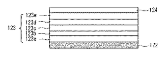
下部電極122上には有機発光層123が位置できる。有機発光層123はサブピクセルに従って、赤色、緑色、及び青色のうち、いずれか1つの色を発光するように形成されることができる。
An organic
有機発光層123上には上部電極124が位置できる。上部電極124は全てのサブピクセルの上部の全体に共通に形成されることができる。このような上部電極124はアノードに選択されることができる。アノードに選択された上部電極124は、ITO、IZO、ITZO、AZOのように、透明な材料を使用することができるが、これに限定されるのではない。
An
以下、図3を参照して有機発光層123を含む有機発光ダイオードについて、より詳細に説明する。
Hereinafter, the organic light emitting diode including the organic
図3に示すように、有機発光ダイオードは、下部電極122、電子注入層123a、電子輸送層123b、発光層123c、正孔輸送層123d、正孔注入層123e、及び上部電極124を含むことができる。
As shown in FIG. 3, the organic light emitting diode includes a
電子注入層123aは、電子の注入を円滑にする役目をし、Alq3、PBD、TAZ、spiro−PBD、BAlqまたはSAlqを使用できるが、これに限定されるのではない。 The electron injection layer 123a serves to facilitate the injection of electrons, and Alq3, PBD, TAZ, spiro-PBD, BAlq, or SAlq can be used, but is not limited thereto.
電子輸送層123bは、電子の輸送を円滑にする役目をし、Alq3、PBD、TAZ、spiro−PBD、BAlq、及びSAlqからなる群から選択されるいずれか1つ以上でなされることができるが、これに限定されるのではない。
The
発光層123cは、赤色、緑色、青色、及び白色を発光する物質を含むことができ、燐光または蛍光物質を用いて形成することができる。
The light-emitting
発光層123cが赤色の場合、CBP(carbazole biphenyl)、またはmCP(1,3-bis(carbazol-9-yl))を含むホスト物質を含み、PIQIr(acac)(bis(1- phenylisoquinoline) acetylacetonate iridium)、PQIr(acac)bis(1-phenylquinoline)acetylacetonate iridium)、PQIr(tris(1-phenylquinoline)iridium)、及びPtOEP(octaethylporphyrin platinum)からなる群から選択されるいずれか1つ以上を含むドーパントを含む燐光物質からなることができ、これとは異なり、PBD:Eu(DBM)3(Phen)またはPeryleneを含む蛍光物質からなることができるが、これに限定されるのではない。
When the
発光層123cが緑色の場合、CBPまたはmCPを含むホスト物質を含み、Ir(ppy)3(fac tris(2-phenylpyridine)iridium)を含むドーパント物質を含む燐光物質からなることができ、これとは異なり、Alq3を含む蛍光物質からなることができるが、これに限定されるのではない。
When the
発光層123cが青色の場合、CBPまたはmCPを含むホスト物質を含み、(4,6-F2ppy)2Irpicを含むドーパント物質を含む燐光物質からなることができる。これとは異なり、spiro-DPVBi、spiro-6P、ジスチルベンゼン(DSB)、ジスチルアリレン(DSA)、PFO系高分子及びPPV系高分子からなる群から選択されるいずれか1つを含む蛍光物質からなることができるが、これに限定されるのではない。
When the
正孔輸送層123dは、正孔の輸送を円滑にする役目をし、NPD(N,N-dinaphthyl-N、N'-diphenyl benzidine)、TPD(N、N'-bis-3-methylphenyl)-N,N'-bis-(phenyl)-benzidine)、s-TAD、及びMTDATA(4,4',4"-Tris(N-3-methylphenyl-N-phenyl-amino)-triphenylamine)からなる群から選択されるいずれか1つ以上からなることができるが、これに限定されるのではない。
The
正孔注入層123eは、正孔の注入を円滑にする役目をすることができ、CuPc(cupper phthalocyanine)、PEDOT(poly(3,4)-ethylenedioxythiophene)、PANI(polyaniline)、及びNPD(N,N-dinaphthyl-N,N'-diphenyl benzidine)からなる群から選択されるいずれか1つ以上からなることができるが、これに限定されるのではない。
The
ここで、本発明の第1実施形態は、図3に限定されるのではなく、電子注入層123a、電子輸送層123b、正孔輸送層123d、及び正孔注入層123eのうち、少なくともいずれか1つが省略されることもできる。
Here, the first embodiment of the present invention is not limited to FIG. 3, but at least one of the electron injection layer 123a, the
以下、本発明の第1実施形態に係る有機電界発光表示装置の製造方法について説明する。 Hereinafter, a method for manufacturing an organic light emitting display according to the first embodiment of the present invention will be described.
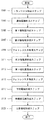
図4及び図5に示すように、基板110上にゲート112a、112b、ソース115a、115c、及びドレイン115b、115dを含むトランジスタを形成するステップ(S101)を実行する。
As shown in FIGS. 4 and 5, a step (S101) of forming
これによって、基板110上には、ゲート112a、112bが位置できる。また、ゲート112a、112b上には第1絶縁膜113が位置できる。また、第1絶縁膜113上にはアクティブ層114a、114bが位置できる。また、アクティブ層114a、114b上にはソース115a、115c及びドレイン115b、115dが位置できる。また、ソース115a、115c及びドレイン115b、115d上には第2絶縁膜116aが位置できる。また、第2絶縁膜116a上には平坦度を高めるための第3絶縁膜116bが位置できる。
As a result, the
ここで、基板110上に位置するトランジスタのうち、ゲート112a、ソース115a、及びドレイン115bは駆動トランジスタであり、ゲート112b、ソース115c、及びドレイン115dはスイッチングトランジスタであることができる。駆動トランジスタのソース115a及びドレイン115bのうちの1つは第2絶縁膜116a上に位置するシールド金属118aに連結されることができる。そして、駆動トランジスタのソース115aまたはドレイン115bのうちの1つは、スイッチングトランジスタのソース115cまたはドレイン115dに連結されることができる。
Here, among the transistors located on the
以上、基板110上に形成されたトランジスタがボトムゲート型であることを一例として説明した。しかしながら、基板110上に形成されるトランジスタはボトムゲート型だけでなくトップゲート型でも形成されることができる。
As described above, the example in which the transistor formed over the
次に、図4及び図5に示すように、トランジスタ上にソース115aまたはドレイン115bに連結される連結電極117を形成するステップS103を実行する。
Next, as shown in FIGS. 4 and 5, step S103 is performed to form a
これによって、トランジスタの第3絶縁膜116b上には駆動トランジスタのソース115aまたはドレイン115bに連結された連結電極117が位置できる。
Accordingly, the
次に、図4及び図6に示すように、連結電極117上に第1犠牲層120を形成するステップS105を実行する。
Next, as shown in FIGS. 4 and 6, Step S <b> 105 is performed to form the first
これによって、連結電極117上には連結電極117の一部を露出する第1犠牲層120が位置できる。第1犠牲層120は、シリコン酸化物(SiOx)、シリコン窒化物(SiNx)のような無機絶縁膜を含むことができる。本発明の第1実施形態では、第1犠牲層120がSiNxであることを一例とする。
Accordingly, the first
次に、図4及び図6に示すように、第1犠牲層120上に第2犠牲層121を形成するステップS107を実行する。
Next, as shown in FIGS. 4 and 6, Step S107 for forming the second
これによって、第1犠牲層120上には連結電極117の一部を露出する第2犠牲層121が位置できる。第2犠牲層121は金属または金属酸化物を含むことができる。本発明の第1実施形態では第2犠牲層121がITOであることを一例とする。
Accordingly, the second
次に、図4及び図6に示すように、第2犠牲層121上に第2犠牲層121の一部が露出されるようにフォトレジスタ(PR)を形成するステップS109を実行する。
Next, as shown in FIGS. 4 and 6, Step S <b> 109 is performed in which a photoresist (PR) is formed on the second
これによって、第2犠牲層121上にはフォトレジスタ(PR)が位置できる。
Accordingly, a photoresist (PR) can be positioned on the second
次に、図4及び図6に示すように、フォトレジスタ(PR)の下部に第2犠牲層121が引き込まれるように第1エッチング方法(E1)を用いて第2犠牲層121を除去するステップS111を実行する。ここで、第1エッチング方法(E1)は湿式エッチング方法を使用することができるが、これに限定されるのではない。
Next, as shown in FIGS. 4 and 6, a step of removing the second
次に、図4及び図6に示すように、第2犠牲層121の下部に第1犠牲層120が引き込まれるように第2エッチング方法(E2)を用いて第1犠牲層120を除去するステップS113を実行する。ここで、第2エッチング方法(E2)は6フッ化硫黄(SF6)と酸素(O2)を含むドライエッチング方法であることができるが、これに限定されるのではない。
Next, as shown in FIGS. 4 and 6, the step of removing the first
但し、第1犠牲層120の除去時に酸素より6フッ化硫黄の割合を高く設定することができる。このような割合で第2エッチング方法(E2)を実行すると、フォトレジスタ(PR)が相対的に少なくエッチングされる。この方法によると、アンダーカットパターンを実行する時、従来のようにエッチング時間を調節しなければならない不便性を改善することができる。
However, when the first
図7には第1犠牲層120の除去時に酸素と6フッ化硫黄の割合に従うエッチング態様が図示される。図7の(a)は第1犠牲層120の除去時に6フッ化硫黄より酸素の割合が大きい場合を示し、図7の(b)は第1犠牲層120の除去時に酸素より6フッ化硫黄の割合が大きい場合を示す。図7から分かるように、第2エッチング方法(E2)により第1犠牲層120を除去する時、酸素より6フッ化硫黄の割合を高く設定すると、第1犠牲層120が第2犠牲層121の内側に一層深く引き込まれることができる。
FIG. 7 illustrates an etching mode according to the ratio of oxygen and sulfur hexafluoride when the first
次に、図4及び図6に示すように、フォトレジスタ(PR)を除去するステップS115を実行する。 Next, as shown in FIGS. 4 and 6, step S115 for removing the photoresistor (PR) is executed.
これによって、第2犠牲層121上に位置するフォトレジスタ(PR)は除去される。
As a result, the photoresist (PR) located on the second
以上のような段階を実行すると、図8に示すような構造で形成される。 When the above steps are executed, a structure as shown in FIG. 8 is formed.
次に、図4及び図9に示すように、連結電極117上に下部電極122を形成するステップS117を実行する。
Next, as shown in FIGS. 4 and 9, Step S <b> 117 for forming the
これによって、連結電極117は勿論、第2犠牲層121上に下部電極122が位置する。下部電極122は、アンダーカットパターンされた第1犠牲層120及び第2犠牲層121により各サブピクセル毎に分離形成されることができる。このような下部電極122は、カソードに選択されることができる。カソードに選択された下部電極122は、アルミニウム(Al)、アルミニウム合金(Al alloy)のように、不透明で、かつ仕事関数が低い材料を使用できるが、これに限定されるのではない。
Accordingly, the
次に、図4及び図9に示すように、下部電極122上に有機発光層123を形成するステップS119を実行する。
Next, as shown in FIGS. 4 and 9, Step S <b> 119 for forming the organic
これによって、下部電極122上には有機発光層123が位置できる。有機発光層123はサブピクセルに従って、赤色、緑色、及び青色のうち、どれか1つの色を発光するように形成することができる。
Accordingly, the organic
次に、図4及び図9に示すように、有機発光層123上に上部電極124を形成するステップS121を実行する。
Next, as shown in FIGS. 4 and 9, step S121 for forming the
これによって、有機発光層123上には上部電極124が位置できる。上部電極124は全てのサブピクセルの上部の全体に共通に形成されることができる。このような上部電極124はアノードに選択されることができる。アノードに選択された上部電極124は、ITO、IZO、ITZO、AZOのように、透明な材料を使用することができるが、これに限定されるのではない。
Accordingly, the
以上、本発明の第1実施形態のように、第1犠牲層120の材料に無機絶縁膜を使用し、第2犠牲層121の材料に金属または金属酸化物を使用すると、アンダーカットパターン時に第1犠牲層120の厚みを500Å以下に薄く形成できるので、アンダーカットによる段差(例えば、有機発光層の段差)により上部電極がオープン(切れ)される問題を防止することができる。また、この場合、アンダーカットパターン時に使われる第1犠牲層120及び第2犠牲層121の厚みを最小化できることは勿論、アンダーカットパターン時の深さも任意に調節できる効果がある。また、アンダーカットパターンを用いて下部電極122を形成し、有機発光層123及び上部電極124を形成するので、下部電極122が酸化される問題を抑制できる効果がある。また、下部電極122の酸化を抑制できるので、電子注入特性を向上させることができることは勿論、発光効率も向上させることができる効果がある。また、第2犠牲層121の材料に金属または金属酸化物を使用するので、下部電極122の抵抗を減らすことができる効果がある。また、第1犠牲層120の材料に無機絶縁膜を使用するので、第1犠牲層120の下部に位置する有機材料によるアウト−ガッシング(out-gassing)影響(例えば、サブピクセル収縮)が最小化できる効果がある。
As described above, when the inorganic
(第2実施形態)
図10を参照すると、基板210上にはゲート212a、212bが位置できる。ゲート212a、212bは、モリブデン(Mo)、アルミニウム(Al)、クロム(Cr)、金(Au)、チタニウム(Ti)、ニッケル(Ni)、ネオジム(Nd)、及び銅(Cu)からなる群から選択されるいずれか1つまたはいずれか2つ以上からなる合金からなることができる。また、ゲート212a、212bは、モリブデン(Mo)、アルミニウム(Al)、クロム(Cr)、金(Au)、チタニウム(Ti)、ニッケル(Ni)、ネオジム(Nd)、及び銅(Cu)からなる群から選択されるいずれか1つまたはいずれか2つ以上からなる合金からなる多重層であることができる。また、ゲート212a、212bは、モリブデン/アルミニウム−ネオジム、またはモリブデン/アルミニウムの2重層であることができる。
(Second Embodiment)
Referring to FIG. 10,
ゲート212a、212b上には第1絶縁膜213が位置できる。第1絶縁膜213は、シリコン酸化物(SiOx)、シリコン窒化物(SiNx)、またはこれらの多重層であることができるが、これに限定されるのではない。
A first insulating
第1絶縁膜213上にはアクティブ層214a、214bが位置できる。アクティブ層214a、214bは、非晶質シリコン、またはこれを結晶化した多結晶シリコンを含むことができる。ここで、図示してはいないが、アクティブ層214a、214bは、チャネル領域、ソース領域、及びドレイン領域を含むことができ、ソース領域及びドレイン領域にはP型またはN型不純物がドーピングされることができる。また、アクティブ層214a、214bは、接触抵抗を低めるためのオーミックコンタクト層を含むこともできる。
アクティブ層214a、214b上にはソース215a、215c及びドレイン215b、215dが位置できる。ソース215a、215c及びドレイン215b、215dは、単一層または多重層からなることができ、ソース215a、215c及びドレイン215b、215dが単一層の場合には、モリブデン(Mo)、アルミニウム(Al)、クロム(Cr)、金(Au)、チタニウム(Ti)、ニッケル(Ni)、ネオジム(Nd)及び銅(Cu)からなる群から選択されるいずれか1つ、またはいずれか2つ以上からなる合金からなることができる。また、ソース215a、215c及びドレイン215b、215dが多重層の場合には、モリブデン/アルミニウム−ネオジムの2重層、モリブデン/アルミニウム/モリブデン、またはモリブデン/アルミニウム−ネオジム/モリブデンの3重層からなることができる。
ソース215a、215c及びドレイン215b、215d上には第2絶縁膜216aが位置できる。第2絶縁膜216aは、シリコン酸化物(SiOx)、シリコン窒化物(SiNx)、またはこれらの多重層であることができるが、これに限定されるのではない。第2絶縁膜216aはパッシベーション膜であることができる。
A second insulating
基板210上に位置するトランジスタのうち、ゲート212a、ソース215a、及びドレイン215bは駆動トランジスタであり、ゲート212b、ソース215c、及びドレイン215dはスイッチングトランジスタであることができる。駆動トランジスタのソース215a及びドレイン215bのうちの1つは第2絶縁膜216a上に位置するシールド金属218aに連結されることができる。そして、駆動トランジスタのソース215aまたはドレイン215bのうちの1つはスイッチングトランジスタのソース215cまたはドレイン215dに連結されることができる。
Of the transistors located on the
第2絶縁膜216a上には平坦度を高めるための第3絶縁膜216bが位置できる。第3絶縁膜216bはポリイミドなどの有機物を含むことができる。
A third
以上、基板210上に形成されたトランジスタがボトムゲート型であることを一例として説明した。しかしながら、基板210上に形成されるトランジスタはボトムゲート型だけでなく、トップゲート型でも形成されることができる。
As described above, the example in which the transistor formed over the
トランジスタの第3絶縁膜216b上には、駆動トランジスタのソース215a、またはドレイン215bに連結された連結電極217が位置できる。
A
連結電極217上には連結電極217の一部を露出する犠牲層220が位置できる。犠牲層220は、シリコン酸化物(SiOx)、シリコン窒化物(SiNx)のような無機絶縁膜を含むことができる。
A
犠牲層220上には連結電極217の一部を露出するバンク層221が位置できる。バンク層221はベンゾサイクロブテン(BCB)系樹脂、アクリル系樹脂、またはポリイミド樹脂などの有機物を含むことができる。
A
一方、連結電極217上に位置する犠牲層220の場合、バンク層221より内側に引き込まれるようにアンダーカットパターンすることができる。すなわち、バンク層221の下に在る犠牲層220がアンダーカットされ、バンク層221のエッジより犠牲層220のエッジが引き込まれるような構成をとることができる。このように犠牲層220の材料に無機絶縁膜を使用し、犠牲層220をアンダーカットパターンすると、アンダーカットパターン時に犠牲層220の厚みを500Å以下に薄く形成できるので、アンダーカットによる段差(例えば、有機発光層の段差)により上部電極が切れる問題を防止することができる。
On the other hand, in the case of the
連結電極217上には下部電極222が位置できる。下部電極222はアンダーカットパターンされた犠牲層220により各サブピクセル毎に分離形成されることができる。このような下部電極222はカソードに選択されることができる。カソードに選択された下部電極222は、アルミニウム(Al)、アルミニウム合金(Al alloy)のように、不透明で、かつ仕事関数が低い材料を使用することができるが、これに限定されるのではない。
A
下部電極222上には有機発光層223が位置できる。有機発光層223はサブピクセルに従って、赤色、緑色、及び青色のうち、どれか1つの色を発光するように形成されることができる。
An organic
有機発光層223上には上部電極224が位置できる。上部電極224は全てのサブピクセルの上部全体に共通に形成されることができる。このような上部電極224はアノードに選択されることができる。アノードに選択された上部電極224は、ITO、IZO、ITZO、AZOのように、透明な材料を使用することができるが、これに限定されるのではない。
An
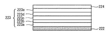
以下、図11を参照して有機発光層223を含む有機発光ダイオードについて概略的に説明する。
Hereinafter, an organic light emitting diode including the organic
図11に示すように、有機発光ダイオードは、下部電極222、電子注入層223a、電子輸送層223b、発光層223c、正孔輸送層223d、正孔注入層223e、及び上部電極224を含むことができる。
As shown in FIG. 11, the organic light emitting diode includes a
しかしながら、本発明の第2実施形態は、図11に限定されるのではなく、電子注入層223a、電子輸送層223b、正孔輸送層223d、及び正孔注入層223eのうち、少なくともいずれか1つが省略されることもできる。
However, the second embodiment of the present invention is not limited to FIG. 11, and at least one of the
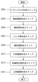
以下、本発明の第2実施形態に係る有機電界発光表示装置の製造方法について説明する。 Hereinafter, a method for manufacturing an organic light emitting display according to the second embodiment of the present invention will be described.
図12及び図13に示すように、基板210上に、ゲート212a、212b、ソース215a、215c、及びドレイン215b、215dを含むトランジスタを形成するステップS201を実行する。
As shown in FIGS. 12 and 13, step S201 for forming
これによって、基板210上には、ゲート212a、212bが位置できる。また、ゲート212a、212b上には第1絶縁膜213が位置できる。また、第1絶縁膜213上にはアクティブ層214a、214bが位置できる。また、アクティブ層214a、214b上には、ソース215a、215c、及びドレイン215b、215dが位置できる。また、ソース215a、215c及びドレイン215b、215d上には、第2絶縁膜216aが位置できる。また、第2絶縁膜216a上には平坦度を高めるための第3絶縁膜216bが位置できる。
As a result, the
ここで、基板210上に位置するトランジスタのうち、ゲート212a、ソース215a、及びドレイン215bは駆動トランジスタであり、ゲート212b、ソース215c、及びドレイン215dはスイッチングトランジスタであることができる。駆動トランジスタのソース215a及びドレイン215bのうちの1つは、第2絶縁膜216a上に位置するシールド金属218aに連結されることができる。そして、駆動トランジスタのソース215aまたはドレイン215bのうちの1つは、スイッチングトランジスタのソース215cまたはドレイン215dに連結されることができる。
Here, among the transistors located on the
以上、基板210上に形成されたトランジスタがボトムゲート型であることを一例として説明した。しかしながら、基板210上に形成されるトランジスタはボトムゲート型だけでなく、トップゲート型でも形成されることができる。
As described above, the example in which the transistor formed over the
次に、図12及び図13に示すように、トランジスタ上にソース214aまたはドレイン214bに連結される連結電極217を形成するステップS203を実行する。
Next, as shown in FIGS. 12 and 13, step S203 is performed to form a
これによって、トランジスタの第3絶縁膜216b上には駆動トランジスタのソース215aまたはドレイン215bに連結された連結電極217が位置できる。
Accordingly, the
次に、図12及び図14に示すように、連結電極217上に犠牲層220を形成するステップS205を実行する。
Next, as shown in FIGS. 12 and 14, Step S <b> 205 for forming the
これによって、連結電極217上には連結電極217の一部を露出する犠牲層220が位置できる。犠牲層220は、シリコン酸化物(SiOx)、シリコン窒化物(SiNx)のような無機絶縁膜を含むことができる。本発明の第2実施形態では犠牲層220がSiNxであることを一例とする。
Accordingly, the
次に、図12及び図14に示すように、犠牲層220上に犠牲層220の一部が露出されるようにバンク層221を形成するステップS207を実行する。
Next, as shown in FIGS. 12 and 14, step S207 is performed to form the
これによって、犠牲層220上には連結電極217の一部を露出するバンク層221が位置できる。バンク層221はベンゾサイクロブテン(BCB)系樹脂、アクリル系樹脂、またはポリイミド樹脂などの有機物を含むことができる。
Accordingly, the
次に、図12及び図14に示すように、バンク層221の下部に犠牲層220が引き込まれるようにエッチング方法(E)を用いて犠牲層220を除去するステップS209を実行する。
Next, as shown in FIGS. 12 and 14, step S209 is performed to remove the
ここで、エッチング方法(E)は、6フッ化硫黄(SF6)と酸素(O2)を含むドライエッチング方法であることができるが、これに限定されるのではない。 Here, the etching method (E) may be a dry etching method including sulfur hexafluoride (SF6) and oxygen (O2), but is not limited thereto.
但し、犠牲層220の除去時に酸素より6フッ化硫黄の割合を高く設定することができる。このような割合でエッチング方法(E)を実行すると、バンク層221が相対的に少なくエッチングされる。この方法によると、アンダーカットパターンを実行する時、従来のようにエッチング時間を調節しなければならない不便性を改善することができる。
However, the ratio of sulfur hexafluoride can be set higher than that of oxygen when the
図15には、犠牲層220の除去時に酸素と6フッ化硫黄の割合に従うエッチング態様が図示される。図15の(a)は犠牲層220の除去時、6フッ化硫黄より酸素の割合が大きい場合を示し、図15の(b)は犠牲層220の除去時、酸素より6フッ化硫黄の割合が大きい場合を示す。図15から分かるように、エッチング方法(E)により犠牲層220を除去する時、酸素より6フッ化硫黄の割合を高く設定すれば、犠牲層220がバンク層221の内側に一層深く引き込まれることができる。
FIG. 15 illustrates an etching mode according to the ratio of oxygen and sulfur hexafluoride when the
以上のようなステップを実行すると、図16に示すような構造で形成される。 When the above steps are executed, a structure as shown in FIG. 16 is formed.
次に、図12及び図17に示すように、連結電極217上に下部電極222を形成するステップS211を実行する。
Next, as shown in FIGS. 12 and 17, Step S <b> 211 in which the
これによって、連結電極217は勿論、バンク層221上に下部電極222が位置する。下部電極222は、アンダーカットパターンされた犠牲層220及びバンク層221により各サブピクセル毎に分離形成されることができる。このような下部電極222はカソードに選択されることができる。カソードに選択された下部電極222は、アルミニウム(Al)、アルミニウム合金(Al alloy)のように、不透明で、かつ仕事関数が低い材料を使用することができるが、これに限定されるのではない。
As a result, the
次に、図12及び図17に示すように、下部電極222上に有機発光層223を形成するステップS213を実行する。
Next, as shown in FIGS. 12 and 17, step S213 for forming the organic
これによって、下部電極222上には有機発光層223が位置できる。有機発光層223はサブピクセルによって、赤色、緑色、及び青色のうち、どれか1つの色を発光するように形成することができる。
Accordingly, the organic
次に、図12及び図17に示すように、有機発光層223上に上部電極224を形成するステップS215を実行する。
Next, as shown in FIGS. 12 and 17, step S215 for forming the
これによって、有機発光層223上には上部電極224が位置できる。上部電極224は全てのサブピクセルの上部全体に共通に形成されることができる。このような上部電極224はアノードに選択されることができる。アノードに選択された上部電極224は、ITO、IZO、ITZO、AZOのように、透明な材料を使用することができるが、これに限定されるのではない。
Accordingly, the
以上、本発明の第2実施形態のように、犠牲層220の材料に無機絶縁膜を使用し、アンダーカットパターン時に犠牲層220の厚みを500Å以下に薄く形成できるので、アンダーカットによる段差(例えば、有機発光層の段差)により上部電極がオープン(切れ)される問題を防止することができる。また、この場合、アンダーカットパターン時に使われる犠牲層220の厚みが最小化できることは勿論、パターンされる深さも任意に調節できる効果がある。また、アンダーカットパターンを用いて下部電極222を形成し、有機発光層223及び上部電極224を形成するので、下部電極222が酸化される問題を抑制できる効果がある。また、下部電極222の酸化を抑制できるので、電子注入特性を向上させることができることは勿論、発光効率も向上させることができる効果がある。また、犠牲層220の材料に無機絶縁膜を使用するので、犠牲層220の下部に位置する有機材料によるアウト−ガッシング(out-gassing)影響(例えば、サブピクセル収縮)を最小化することができる効果が得られる。
As described above, since the inorganic insulating film is used as the material for the
110、210 基板
117、217 連結電極
120 第1犠牲層
121 第2犠牲層
122、222 下部電極
123、223 有機発光層
124、224 上部電極
130 表示部
140 封入基板
150 接着部材
160 駆動部
220 犠牲層
221 バンク層
110, 210
Claims (18)
前記基板上に位置し、ゲート、ソース、及びドレインを含むトランジスタと、
前記トランジスタ上に位置し、前記ソースまたはドレインに連結された連結電極と、
前記連結電極上に位置し、前記連結電極の一部を露出する第1犠牲層と、
前記第1犠牲層上に位置し、前記連結電極の一部を露出する第2犠牲層と、
前記連結電極と前記第2犠牲層上に位置する下部電極と、
前記下部電極上に位置する有機発光層と、
前記有機発光層上に位置する上部電極と、を含み、
前記第1犠牲層が前記第2犠牲層より内側に引き込まれていることを特徴とする有機電界発光表示装置。 A substrate,
A transistor located on the substrate and including a gate, a source, and a drain;
A connection electrode located on the transistor and connected to the source or drain;
A first sacrificial layer located on the connection electrode and exposing a portion of the connection electrode;
A second sacrificial layer located on the first sacrificial layer and exposing a portion of the connection electrode;
A lower electrode positioned on the connection electrode and the second sacrificial layer;
An organic light emitting layer located on the lower electrode;
An upper electrode located on the organic light emitting layer,
The organic electroluminescent display device, wherein the first sacrificial layer is drawn inward from the second sacrificial layer.
前記基板上に位置し、ゲート、ソース、及びドレインを含むトランジスタと、
前記トランジスタ上に位置し、前記ソースまたはドレインに連結された連結電極と、
前記連結電極上に位置し、前記連結電極の一部を露出する第1犠牲層と、
前記第1犠牲層上に位置し、前記連結電極の一部を露出する第2犠牲層と、
前記連結電極と前記第2犠牲層上に位置する下部電極と、
前記下部電極上に位置する有機発光層と、
前記有機発光層上に位置する上部電極と、を含み、
前記第2犠牲層の下に在る前記第1犠牲層がアンダーカットされ、前記第2犠牲層のエッジより前記第1犠牲層のエッジが引き込まれていることを特徴とする有機電界発光装置。 A substrate,
A transistor located on the substrate and including a gate, a source, and a drain;
A connection electrode located on the transistor and connected to the source or drain;
A first sacrificial layer located on the connection electrode and exposing a portion of the connection electrode;
A second sacrificial layer located on the first sacrificial layer and exposing a portion of the connection electrode;
A lower electrode positioned on the connection electrode and the second sacrificial layer;
An organic light emitting layer located on the lower electrode;
An upper electrode located on the organic light emitting layer,
The organic electroluminescent device according to claim 1, wherein the first sacrificial layer under the second sacrificial layer is undercut, and an edge of the first sacrificial layer is drawn from an edge of the second sacrificial layer.
前記基板上に位置し、ゲート、ソース、及びドレインを含むトランジスタと、
前記トランジスタ上に位置し、前記ソースまたはドレインに連結された連結電極と、
前記連結電極上に位置し、前記連結電極の一部を露出する犠牲層と、
前記犠牲層上に位置し、前記連結電極の一部を露出するバンク層と、
前記連結電極と前記バンク層上に位置する下部電極と、
前記下部電極上に位置する有機発光層と、
前記有機発光層上に位置する上部電極と、を含み、
前記犠牲層が前記バンク層より内側に引き込まれていることを特徴とする有機電界発光表示装置。 A substrate,
A transistor located on the substrate and including a gate, a source, and a drain;
A connection electrode located on the transistor and connected to the source or drain;
A sacrificial layer located on the connection electrode and exposing a portion of the connection electrode;
A bank layer located on the sacrificial layer and exposing a portion of the connection electrode;
A lower electrode located on the connection electrode and the bank layer;
An organic light emitting layer located on the lower electrode;
An upper electrode located on the organic light emitting layer,
An organic electroluminescent display device, wherein the sacrificial layer is drawn inward from the bank layer.
前記基板上に位置し、ゲート、ソース、及びドレインを含むトランジスタと、
前記トランジスタ上に位置し、前記ソースまたはドレインに連結された連結電極と、
前記連結電極上に位置し、前記連結電極の一部を露出する犠牲層と、
前記犠牲層上に位置し、前記連結電極の一部を露出するバンク層と、
前記連結電極と前記バンク層上に位置する下部電極と、
前記下部電極上に位置する有機発光層と、
前記有機発光層上に位置する上部電極と、を含み、
前記バンク層の下に在る前記犠牲層がアンダーカットされ、前記バンク層のエッジより前記犠牲層のエッジが引き込まれていることを特徴とする有機電界発光装置。 A substrate,
A transistor located on the substrate and including a gate, a source, and a drain;
A connection electrode located on the transistor and connected to the source or drain;
A sacrificial layer located on the connection electrode and exposing a portion of the connection electrode;
A bank layer located on the sacrificial layer and exposing a portion of the connection electrode;
A lower electrode located on the connection electrode and the bank layer;
An organic light emitting layer located on the lower electrode;
An upper electrode located on the organic light emitting layer,
The organic electroluminescence device according to claim 1, wherein the sacrificial layer under the bank layer is undercut, and an edge of the sacrificial layer is drawn from an edge of the bank layer.
前記トランジスタ上に前記ソースまたは前記ドレインに連結される連結電極を形成するステップと、
前記連結電極上に第1犠牲層を形成するステップと、
前記第1犠牲層上に第2犠牲層を形成するステップと、
前記第2犠牲層上に前記第2犠牲層の一部が露出されるようにフォトレジスタを形成するステップと、
前記フォトレジスタの下部に前記第2犠牲層が引き込まれるように第1エッチング方法を用いて前記第2犠牲層を除去するステップと、
前記第2犠牲層の下部に前記第1犠牲層が引き込まれるように第2エッチング方法を用いて前記第1犠牲層を除去するステップと、
前記フォトレジスタを除去するステップと、
前記連結電極上に下部電極を形成するステップと、
前記下部電極上に有機発光層を形成するステップと、
前記有機発光層上に上部電極を形成するステップと、
を含むことを特徴とする有機電界発光表示装置の製造方法。 Forming a transistor including a gate, a source, and a drain on a substrate;
Forming a connection electrode connected to the source or the drain on the transistor;
Forming a first sacrificial layer on the connection electrode;
Forming a second sacrificial layer on the first sacrificial layer;
Forming a photoresist so that a portion of the second sacrificial layer is exposed on the second sacrificial layer;
Removing the second sacrificial layer using a first etching method so that the second sacrificial layer is drawn under the photoresist;
Removing the first sacrificial layer using a second etching method such that the first sacrificial layer is drawn below the second sacrificial layer;
Removing the photoresistor;
Forming a lower electrode on the connection electrode;
Forming an organic light emitting layer on the lower electrode;
Forming an upper electrode on the organic light emitting layer;
A method for manufacturing an organic light emitting display device, comprising:
前記トランジスタ上に前記ソースまたは前記ドレインに連結される連結電極を形成するステップと、
前記連結電極上に第1犠牲層を形成するステップと、
前記第1犠牲層上に第2犠牲層を形成するステップと、
前記第2犠牲層上に前記第2犠牲層の一部が露出されるようにフォトレジスタを形成するステップと、
前記フォトレジスタの下部に在る前記第2犠牲層がアンダーカットされ、前記フォトレジスタのエッジより前記第2犠牲層のエッジが引き込まれるように第1エッチング方法を用いて前記第2犠牲層を除去するステップと、
前記第2犠牲層の下部に在る前記第1犠牲層がアンダーカットされ、前記第2犠牲層のエッジより前記第1犠牲層のエッジが引き込まれるように第2エッチング方法を用いて前記第1犠牲層を除去するステップと、
前記フォトレジスタを除去するステップと、
前記連結電極上に下部電極を形成するステップと、
前記下部電極上に有機発光層を形成するステップと、
前記有機発光層上に上部電極を形成するステップと、
を含むことを特徴とする有機電界発光表示装置の製造方法。 Forming a transistor including a gate, a source, and a drain on a substrate;
Forming a connection electrode connected to the source or the drain on the transistor;
Forming a first sacrificial layer on the connection electrode;
Forming a second sacrificial layer on the first sacrificial layer;
Forming a photoresist so that a portion of the second sacrificial layer is exposed on the second sacrificial layer;
The second sacrificial layer under the photoresist is undercut, and the second sacrificial layer is removed using a first etching method so that the edge of the second sacrificial layer is drawn from the edge of the photoresist. And steps to
The first sacrificial layer under the second sacrificial layer is undercut, and the first sacrificial layer edge is drawn from the edge of the second sacrificial layer using the second etching method. Removing the sacrificial layer;
Removing the photoresistor;
Forming a lower electrode on the connection electrode;
Forming an organic light emitting layer on the lower electrode;
Forming an upper electrode on the organic light emitting layer;
A method for manufacturing an organic light emitting display device, comprising:
前記トランジスタ上に前記ソースまたは前記ドレインに連結される連結電極を形成するステップと、
前記連結電極上に犠牲層を形成するステップと、
前記犠牲層上に前記犠牲層の一部が露出されるようにバンク層を形成するステップと、
前記バンク層の下部に前記犠牲層が引き込まれるようにエッチング方法を用いて前記犠牲層を除去するステップと、
前記連結電極上に下部電極を形成するステップと、
前記下部電極上に有機発光層を形成するステップと、
前記有機発光層上に上部電極を形成するステップと、
を含むことを特徴とする、有機電界発光表示装置の製造方法。 Forming a transistor including a gate, a source, and a drain on a substrate;
Forming a connection electrode connected to the source or the drain on the transistor;
Forming a sacrificial layer on the connection electrode;
Forming a bank layer on the sacrificial layer such that a portion of the sacrificial layer is exposed;
Removing the sacrificial layer using an etching method so that the sacrificial layer is drawn under the bank layer;
Forming a lower electrode on the connection electrode;
Forming an organic light emitting layer on the lower electrode;
Forming an upper electrode on the organic light emitting layer;
A method for manufacturing an organic light emitting display device, comprising:
前記トランジスタ上に前記ソースまたは前記ドレインに連結される連結電極を形成するステップと、
前記連結電極上に犠牲層を形成するステップと、
前記犠牲層上に前記犠牲層の一部が露出されるようにバンク層を形成するステップと、
前記バンク層の下部に在る前記犠牲層がアンダーカットされ、前記バック層のエッジより前記犠牲層のエッジが引き込まれるようにエッチング方法を用いて前記犠牲層を除去するステップと、
前記連結電極上に下部電極を形成するステップと、
前記下部電極上に有機発光層を形成するステップと、
前記有機発光層上に上部電極を形成するステップと、
を含むことを特徴とする、有機電界発光表示装置の製造方法。 Forming a transistor including a gate, a source, and a drain on a substrate;
Forming a connection electrode connected to the source or the drain on the transistor;
Forming a sacrificial layer on the connection electrode;
Forming a bank layer on the sacrificial layer such that a portion of the sacrificial layer is exposed;
Removing the sacrificial layer using an etching method such that the sacrificial layer under the bank layer is undercut and the edge of the sacrificial layer is drawn from the edge of the back layer;
Forming a lower electrode on the connection electrode;
Forming an organic light emitting layer on the lower electrode;
Forming an upper electrode on the organic light emitting layer;
A method for manufacturing an organic light emitting display device, comprising:
Applications Claiming Priority (2)
| Application Number | Priority Date | Filing Date | Title |
|---|---|---|---|
| KR1020080069505A KR101310917B1 (en) | 2008-07-17 | 2008-07-17 | Organic Light Emitting Display and Manufacturing Method of the same |
| KR10-2008-0069505 | 2008-07-17 |
Publications (2)
| Publication Number | Publication Date |
|---|---|
| JP2010027591A true JP2010027591A (en) | 2010-02-04 |
| JP4806001B2 JP4806001B2 (en) | 2011-11-02 |
Family
ID=41529711
Family Applications (1)
| Application Number | Title | Priority Date | Filing Date |
|---|---|---|---|
| JP2008317928A Active JP4806001B2 (en) | 2008-07-17 | 2008-12-15 | Organic electroluminescent display device and manufacturing method thereof |
Country Status (4)
| Country | Link |
|---|---|
| US (1) | US7902746B2 (en) |
| JP (1) | JP4806001B2 (en) |
| KR (1) | KR101310917B1 (en) |
| CN (1) | CN101630689B (en) |
Cited By (9)
| Publication number | Priority date | Publication date | Assignee | Title |
|---|---|---|---|---|
| WO2014034814A1 (en) | 2012-08-31 | 2014-03-06 | 富士フイルム株式会社 | Dispersion composition, and curable composition, transparent film, microlens and solid-state imaging element using same |
| WO2014034813A1 (en) | 2012-08-31 | 2014-03-06 | 富士フイルム株式会社 | Dispersion composition, and curable composition, transparent film, microlens and solid-state imaging element using same, and polymer compound |
| WO2014034815A1 (en) | 2012-08-31 | 2014-03-06 | 富士フイルム株式会社 | Dispersion composition, and curable composition, transparent film, microlens and solid-state imaging element using same |
| US9087964B2 (en) | 2012-10-17 | 2015-07-21 | Semiconductor Energy Laboratory Co., Ltd. | Light-emitting device |
| US9093404B2 (en) | 2012-12-21 | 2015-07-28 | Semiconductor Energy Laboratory Co., Ltd. | Light-emitting device and method for manufacturing the same |
| US9209355B2 (en) | 2013-03-08 | 2015-12-08 | Semiconductor Energy Laboratory Co., Ltd. | Light-emitting device |
| US9231042B2 (en) | 2013-02-12 | 2016-01-05 | Semiconductor Energy Laboratory Co., Ltd. | Light-emitting device |
| US9728693B2 (en) | 2012-10-17 | 2017-08-08 | Semiconductor Energy Laboratory Co., Ltd. | Light-emitting device comprising partition including overhang portion |
| WO2021149422A1 (en) * | 2020-01-22 | 2021-07-29 | ソニーグループ株式会社 | Display device, display device manufacturing method, and electronic device |
Families Citing this family (23)
| Publication number | Priority date | Publication date | Assignee | Title |
|---|---|---|---|---|
| KR101456154B1 (en) | 2009-08-25 | 2014-11-04 | 삼성디스플레이 주식회사 | Organic light emitting diode lighting apparatus |
| KR101174881B1 (en) * | 2010-06-11 | 2012-08-17 | 삼성디스플레이 주식회사 | Organic light emitting display and manufacturing method thereof |
| CN103928488B (en) * | 2013-06-19 | 2017-04-05 | 上海天马微电子有限公司 | Organic luminous panel and device and its preparation, short-circuit detecting and short-circuit restorative procedure |
| KR102210729B1 (en) * | 2013-12-02 | 2021-02-02 | 엘지디스플레이 주식회사 | Organic Light Emitting Display Device and Method of manufacturing the same |
| KR102155815B1 (en) * | 2014-08-05 | 2020-09-14 | 엘지디스플레이 주식회사 | Organic light emitting display device |
| JP2016081562A (en) * | 2014-10-09 | 2016-05-16 | ソニー株式会社 | Display apparatus, manufacturing method of the same, and electronic apparatus |
| KR102575459B1 (en) * | 2015-07-31 | 2023-09-06 | 엘지디스플레이 주식회사 | Organic light emitting display device and method for fabricating thereof |
| KR102453820B1 (en) * | 2015-08-21 | 2022-10-17 | 서울반도체 주식회사 | Driving circuit and lighting apparatus for light emitting diode |
| KR102367215B1 (en) * | 2015-08-31 | 2022-02-24 | 엘지디스플레이 주식회사 | Organic Light Emitting Display Device |
| KR102474203B1 (en) * | 2015-12-22 | 2022-12-06 | 삼성디스플레이 주식회사 | Method for manufacturing display apparatus and display apparatus manufactured using the same |
| KR102536146B1 (en) * | 2016-04-07 | 2023-05-24 | 삼성전자주식회사 | Display device, electronic apparatus comprising the same and operating method thereof |
| KR102631260B1 (en) * | 2016-04-08 | 2024-01-31 | 삼성디스플레이 주식회사 | Display apparatus and method thereof |
| KR102610028B1 (en) * | 2016-04-12 | 2023-12-06 | 삼성디스플레이 주식회사 | Display device |
| KR101878187B1 (en) * | 2016-07-29 | 2018-07-13 | 엘지디스플레이 주식회사 | Organic light emitting display and fabricating method thereof |
| KR102520696B1 (en) * | 2017-06-02 | 2023-04-12 | 엘지디스플레이 주식회사 | Light Emitting Display Device and Manufacturing Method of the same |
| CN107331647B (en) | 2017-06-14 | 2019-07-23 | 京东方科技集团股份有限公司 | A kind of display base plate and preparation method thereof, display device |
| CN107565049B (en) * | 2017-08-25 | 2019-11-01 | 京东方科技集团股份有限公司 | AMOLED display panel and preparation method thereof |
| KR102374753B1 (en) * | 2017-09-04 | 2022-03-15 | 엘지디스플레이 주식회사 | Light Emitting Display Device and Manufacturing Method thereof |
| KR102514205B1 (en) * | 2017-12-07 | 2023-03-27 | 엘지디스플레이 주식회사 | Organic light emitting display device |
| KR102439307B1 (en) | 2018-01-29 | 2022-09-02 | 삼성디스플레이 주식회사 | organic light emitting display device and Manufacturing method of the same |
| KR102573550B1 (en) * | 2018-08-31 | 2023-08-31 | 엘지디스플레이 주식회사 | Light Emitting Display Device and Manufacturing Method thereof |
| KR20200082986A (en) * | 2018-12-31 | 2020-07-08 | 엘지디스플레이 주식회사 | Electroluminescent Light Emitting Display Apparatus and Method for Manufacturing the Same |
| KR20200087912A (en) * | 2019-01-11 | 2020-07-22 | 삼성디스플레이 주식회사 | Organic light emitting diode display device and method of manufacturing organic light emitting diode display device |
Citations (3)
| Publication number | Priority date | Publication date | Assignee | Title |
|---|---|---|---|---|
| JP2006080054A (en) * | 2004-09-08 | 2006-03-23 | Samsung Sdi Co Ltd | Organic electroluminescent display device and its manufacturing method |
| WO2008013402A1 (en) * | 2006-07-25 | 2008-01-31 | Lg Chem, Ltd. | Method of manufacturing organic light emitting device and organic light emitting device manufactured by using the method |
| JP2008235248A (en) * | 2007-03-22 | 2008-10-02 | Lg Display Co Ltd | Display base, organic light-emitting diode display device therewith, and method of manufacture |
Family Cites Families (9)
| Publication number | Priority date | Publication date | Assignee | Title |
|---|---|---|---|---|
| WO2002037518A1 (en) * | 2000-11-06 | 2002-05-10 | Fujitsu Limited | Field-emission cathode and method for manufacturing the same |
| EP1505666B1 (en) * | 2003-08-05 | 2018-04-04 | LG Display Co., Ltd. | Top-emission active matrix organic electroluminescent display device and method for fabricating the same |
| US7227306B2 (en) * | 2003-08-28 | 2007-06-05 | Samsung Sdi Co., Ltd. | Organic electroluminescence display having recessed electrode structure |
| KR100544138B1 (en) * | 2003-11-12 | 2006-01-23 | 삼성에스디아이 주식회사 | Active matrix type organic electroluminescence device |
| KR100685841B1 (en) * | 2005-12-09 | 2007-02-22 | 삼성에스디아이 주식회사 | Oled and method of fabricting the same |
| KR101338748B1 (en) * | 2006-06-30 | 2013-12-06 | 엘지디스플레이 주식회사 | Organic light emitting device and method of manufacturing thereof |
| KR100859084B1 (en) * | 2006-07-25 | 2008-09-17 | 주식회사 엘지화학 | Organic Light Emitting Diode And Method For Preparing Thereof |
| KR100884185B1 (en) * | 2006-07-25 | 2009-02-17 | 주식회사 엘지화학 | Organic Light Emitting Diode And Method For Preparing Thereof |
| KR100796618B1 (en) * | 2007-01-04 | 2008-01-22 | 삼성에스디아이 주식회사 | Organic light emitting diode display and method for fabricating of the same |
-
2008
- 2008-07-17 KR KR1020080069505A patent/KR101310917B1/en active IP Right Grant
- 2008-11-20 CN CN2008101810528A patent/CN101630689B/en active Active
- 2008-12-15 JP JP2008317928A patent/JP4806001B2/en active Active
- 2008-12-16 US US12/314,777 patent/US7902746B2/en active Active
Patent Citations (3)
| Publication number | Priority date | Publication date | Assignee | Title |
|---|---|---|---|---|
| JP2006080054A (en) * | 2004-09-08 | 2006-03-23 | Samsung Sdi Co Ltd | Organic electroluminescent display device and its manufacturing method |
| WO2008013402A1 (en) * | 2006-07-25 | 2008-01-31 | Lg Chem, Ltd. | Method of manufacturing organic light emitting device and organic light emitting device manufactured by using the method |
| JP2008235248A (en) * | 2007-03-22 | 2008-10-02 | Lg Display Co Ltd | Display base, organic light-emitting diode display device therewith, and method of manufacture |
Cited By (11)
| Publication number | Priority date | Publication date | Assignee | Title |
|---|---|---|---|---|
| WO2014034814A1 (en) | 2012-08-31 | 2014-03-06 | 富士フイルム株式会社 | Dispersion composition, and curable composition, transparent film, microlens and solid-state imaging element using same |
| WO2014034813A1 (en) | 2012-08-31 | 2014-03-06 | 富士フイルム株式会社 | Dispersion composition, and curable composition, transparent film, microlens and solid-state imaging element using same, and polymer compound |
| WO2014034815A1 (en) | 2012-08-31 | 2014-03-06 | 富士フイルム株式会社 | Dispersion composition, and curable composition, transparent film, microlens and solid-state imaging element using same |
| EP3124548A1 (en) | 2012-08-31 | 2017-02-01 | FUJIFILM Corporation | Dispersion composition, curable composition using the same, transparent film, microlens, and solid-state imaging device |
| EP3135733A1 (en) | 2012-08-31 | 2017-03-01 | FUJIFILM Corporation | Dispersion composition, and curable composition, transparent film, microlens and solid-state imaging element using same |
| US9087964B2 (en) | 2012-10-17 | 2015-07-21 | Semiconductor Energy Laboratory Co., Ltd. | Light-emitting device |
| US9728693B2 (en) | 2012-10-17 | 2017-08-08 | Semiconductor Energy Laboratory Co., Ltd. | Light-emitting device comprising partition including overhang portion |
| US9093404B2 (en) | 2012-12-21 | 2015-07-28 | Semiconductor Energy Laboratory Co., Ltd. | Light-emitting device and method for manufacturing the same |
| US9231042B2 (en) | 2013-02-12 | 2016-01-05 | Semiconductor Energy Laboratory Co., Ltd. | Light-emitting device |
| US9209355B2 (en) | 2013-03-08 | 2015-12-08 | Semiconductor Energy Laboratory Co., Ltd. | Light-emitting device |
| WO2021149422A1 (en) * | 2020-01-22 | 2021-07-29 | ソニーグループ株式会社 | Display device, display device manufacturing method, and electronic device |
Also Published As
| Publication number | Publication date |
|---|---|
| CN101630689B (en) | 2011-11-23 |
| KR101310917B1 (en) | 2013-09-25 |
| US20100013379A1 (en) | 2010-01-21 |
| KR20100008891A (en) | 2010-01-27 |
| JP4806001B2 (en) | 2011-11-02 |
| US7902746B2 (en) | 2011-03-08 |
| CN101630689A (en) | 2010-01-20 |
Similar Documents
| Publication | Publication Date | Title |
|---|---|---|
| JP4806001B2 (en) | Organic electroluminescent display device and manufacturing method thereof | |
| JP7127802B2 (en) | Display device with touch detection function and manufacturing method thereof | |
| US8237159B2 (en) | Organic electroluminescent display device and method of manufacturing the same | |
| KR102584253B1 (en) | Organic light emitting display apparatus and method for manufacturing the same | |
| CN105590953B (en) | Organic light emitting diode display with high aperture ratio and its manufacturing method | |
| KR101698543B1 (en) | Organic Light Emitting Device and Method of manufacturing the same | |
| JP2013054863A (en) | Organic el display device, manufacturing method of organic el display device and electronic apparatus | |
| US11081538B2 (en) | Organic light emitting diode display device having a circuit structure buried in a substrate thereof | |
| KR20100065745A (en) | Organic light emitting display device and repairing method thereof | |
| KR20130015113A (en) | Organic light emitting display device and manufacturing method of the same | |
| KR101352237B1 (en) | Organic Light Emitting Display and Manufacturing Method of the same | |
| CN115485849A (en) | Display device, display panel and manufacturing method thereof, driving circuit and driving method | |
| KR20090105208A (en) | Organic Light Emitting Display | |
| KR20110135045A (en) | Organic light emitting display device | |
| KR101570533B1 (en) | Organic Light Emitting Display Device | |
| KR101577819B1 (en) | organic light emitting display | |
| KR101510903B1 (en) | Thin Film Transistor Substrate and Organic Light Emitting Display Device using the same | |
| KR101939798B1 (en) | Organic Light Emitting Display Device | |
| KR101678206B1 (en) | Organic Light Emitting Display Device | |
| KR20100013522A (en) | Manufacturing method for organic light emitting display | |
| KR101572264B1 (en) | Organic Light Emitting Display Device and Manufacturing Method of the same | |
| KR101424272B1 (en) | Organic Light Emitting Display and Manufacturing Method for the same | |
| KR20100008179A (en) | Organic light emitting display and manufacturing method of the same | |
| KR20100016783A (en) | Organic light emitting display and manufacturing method for the same | |
| KR20110049532A (en) | Organic light emitting display device and manufacturing method thereof |
Legal Events
| Date | Code | Title | Description |
|---|---|---|---|
| A977 | Report on retrieval |
Free format text: JAPANESE INTERMEDIATE CODE: A971007 Effective date: 20110217 |
|
| A131 | Notification of reasons for refusal |
Free format text: JAPANESE INTERMEDIATE CODE: A131 Effective date: 20110330 |
|
| A521 | Request for written amendment filed |
Free format text: JAPANESE INTERMEDIATE CODE: A523 Effective date: 20110630 |
|
| TRDD | Decision of grant or rejection written | ||
| A01 | Written decision to grant a patent or to grant a registration (utility model) |
Free format text: JAPANESE INTERMEDIATE CODE: A01 Effective date: 20110719 |
|
| A01 | Written decision to grant a patent or to grant a registration (utility model) |
Free format text: JAPANESE INTERMEDIATE CODE: A01 |
|
| A61 | First payment of annual fees (during grant procedure) |
Free format text: JAPANESE INTERMEDIATE CODE: A61 Effective date: 20110811 |
|
| R150 | Certificate of patent or registration of utility model |
Ref document number: 4806001 Country of ref document: JP Free format text: JAPANESE INTERMEDIATE CODE: R150 Free format text: JAPANESE INTERMEDIATE CODE: R150 |
|
| FPAY | Renewal fee payment (event date is renewal date of database) |
Free format text: PAYMENT UNTIL: 20140819 Year of fee payment: 3 |
|
| R250 | Receipt of annual fees |
Free format text: JAPANESE INTERMEDIATE CODE: R250 |
|
| R250 | Receipt of annual fees |
Free format text: JAPANESE INTERMEDIATE CODE: R250 |
|
| R250 | Receipt of annual fees |
Free format text: JAPANESE INTERMEDIATE CODE: R250 |
|
| R250 | Receipt of annual fees |
Free format text: JAPANESE INTERMEDIATE CODE: R250 |
|
| R250 | Receipt of annual fees |
Free format text: JAPANESE INTERMEDIATE CODE: R250 |
|
| R250 | Receipt of annual fees |
Free format text: JAPANESE INTERMEDIATE CODE: R250 |
|
| R250 | Receipt of annual fees |
Free format text: JAPANESE INTERMEDIATE CODE: R250 |
|
| R250 | Receipt of annual fees |
Free format text: JAPANESE INTERMEDIATE CODE: R250 |
|
| R250 | Receipt of annual fees |
Free format text: JAPANESE INTERMEDIATE CODE: R250 |
|
| R250 | Receipt of annual fees |
Free format text: JAPANESE INTERMEDIATE CODE: R250 |