JP2010026294A - Fail-safe circuit and control circuit - Google Patents
Fail-safe circuit and control circuit Download PDFInfo
- Publication number
- JP2010026294A JP2010026294A JP2008188349A JP2008188349A JP2010026294A JP 2010026294 A JP2010026294 A JP 2010026294A JP 2008188349 A JP2008188349 A JP 2008188349A JP 2008188349 A JP2008188349 A JP 2008188349A JP 2010026294 A JP2010026294 A JP 2010026294A
- Authority
- JP
- Japan
- Prior art keywords
- signal
- clock
- determination
- circuit
- synchronization
- Prior art date
- Legal status (The legal status is an assumption and is not a legal conclusion. Google has not performed a legal analysis and makes no representation as to the accuracy of the status listed.)
- Granted
Links
Images


Abstract
Description
この発明は、画像表示装置を制御するためのタイミング信号を出力する回路に関し、特に画像表示装置を安全に動作させるためにタイミング信号の出力を制御するフェイルセーフ回路及びこのフェイルセーフ回路を含む制御回路に関する。 The present invention relates to a circuit that outputs a timing signal for controlling an image display device, and more particularly to a fail-safe circuit that controls output of a timing signal in order to operate the image display device safely and a control circuit including the fail-safe circuit. About.
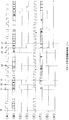
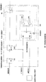
図20を参照して、画像表示装置として液晶表示装置を駆動する制御回路の従来例について説明する(例えば、特許文献1参照)。図20は、制御回路の従来例の概略構成図である。 A conventional example of a control circuit for driving a liquid crystal display device as an image display device will be described with reference to FIG. 20 (see, for example, Patent Document 1). FIG. 20 is a schematic configuration diagram of a conventional control circuit.
制御回路18には、水平垂直同期信号を含む画像信号と、ピクセルクロックが入力される。ピクセルクロックは、画像信号に含まれており、前段に設けられた他の回路(図示を省略する。)で抽出されているものとする。 An image signal including a horizontal / vertical synchronizing signal and a pixel clock are input to the control circuit 18. The pixel clock is included in the image signal and is extracted by another circuit (not shown) provided in the previous stage.
制御回路18は、タイミング信号生成回路21及びフェイルセーフ回路38を備えて構成される。フェイルセーフ回路38は、判定部48と保護ゲート部90とを備えている。
The control circuit 18 includes a timing signal generation circuit 21 and a fail safe circuit 38. The fail safe circuit 38 includes a determination unit 48 and a
制御回路18に入力された画像信号は、タイミング信号生成回路21に送られる。また、制御回路18に入力されたピクセルクロックは2分岐される。ピクセルクロックが2分岐された一方は、タイミング信号生成回路21に送られ、他方は、フェイルセーフ回路38の判定部48に送られる。 The image signal input to the control circuit 18 is sent to the timing signal generation circuit 21. Further, the pixel clock input to the control circuit 18 is branched into two. One of the two branched pixel clocks is sent to the timing signal generation circuit 21, and the other is sent to the determination unit 48 of the fail safe circuit 38.
タイミング信号生成回路21は、画像信号に含まれる水平垂直同期信号を用いて、スタートパルスを含むタイミング信号を生成する。このとき、タイミング信号生成回路21は、クロック入力端子CKに入力されたピクセルクロックを用いて信号処理を行う。 The timing signal generation circuit 21 generates a timing signal including a start pulse using a horizontal / vertical synchronization signal included in the image signal. At this time, the timing signal generation circuit 21 performs signal processing using the pixel clock input to the clock input terminal CK.
タイミング信号生成回路21で生成されたタイミング信号は、フェイルセーフ回路38の保護ゲート部90に送られる。また、タイミング信号生成回路21は、スタートパルスの立ち上げのトリガとして用いた信号を、そのままトリガ信号として出力する。このトリガ信号は、フェイルセーフ回路38の判定部48に送られる。
The timing signal generated by the timing signal generation circuit 21 is sent to the
判定部48は、トリガ信号の入力に応答して、ピクセルクロックの計数を開始する。判定部48は、ピクセルクロックに含まれているクロックパルスの計数を行っている間は、Hレベルの信号を判定信号として出力する。判定部48は、ピクセルクロックの計数を行った結果、計数値が予め設定されている所定の値‘N’に達すると、計数値を0にリセットすると共に、判定信号の出力レベルをLレベルとする。 The determination unit 48 starts counting the pixel clock in response to the input of the trigger signal. The determination unit 48 outputs an H level signal as a determination signal while counting the clock pulses included in the pixel clock. As a result of counting the pixel clock, the determination unit 48 resets the count value to 0 and sets the output level of the determination signal to L level when the count value reaches a predetermined value 'N' set in advance. To do.
この判定信号は、保護ゲート部90に送られ、いわゆるゲート信号として用いられる。保護ゲート部90は、判定信号がHレベルのとき、タイミング信号を通過させ、出力信号として出力する。一方、判定信号がLレベルのとき、保護ゲート部90は、タイミング信号を遮断する。
This determination signal is sent to the
この制御回路の従来例によれば、タイミング信号に含まれるスタートパルスがHレベルになったままになるような誤動作が発生しても、判定信号が一定の期間でLレベルとなり、タイミング信号を遮断するので、後段に設けられる画像表示装置の暴走を抑えることができる。
しかしながら、上述の制御回路の従来例では、トリガ信号が入力される都度、判定部で生成される判定信号がLレベルからHレベルとなり、ピクセルクロックの計数値によって定まる一定期間経過後にHレベルからLレベルになる。従って、この判定信号の論理レベルは、制御回路に入力される画像信号やピクセルクロックの正常状態や異常状態に一意に対応していない。このことから、上述の従来例のフェイルセーフ回路には、スタートパルスが長くなりすぎるのを防ぐ働きしか期待できない。すなわち、異常状態のときに、制御回路に含まれる各内部回路をリセット状態にするような目的での、判定信号の使用は困難である。 However, in the above-described conventional example of the control circuit, each time a trigger signal is input, the determination signal generated by the determination unit changes from L level to H level, and after a certain period determined by the count value of the pixel clock, Become a level. Therefore, the logical level of the determination signal does not uniquely correspond to the normal state or abnormal state of the image signal or pixel clock input to the control circuit. For this reason, the conventional fail-safe circuit can only be expected to prevent the start pulse from becoming too long. That is, it is difficult to use the determination signal for the purpose of resetting each internal circuit included in the control circuit in an abnormal state.
また、何らかの事情でピクセルクロックの入力が停止した場合、判定部では、計数値が所定の値Nに達しないので、判定信号がHレベルになったままになる場合がある。この場合は、スタートパルスが長くなるのを防ぐことができず、後段の画像表示装置を破壊する恐れが出てくる。 Further, when the input of the pixel clock is stopped for some reason, the determination unit may remain at the H level because the count value does not reach the predetermined value N in the determination unit. In this case, it is impossible to prevent the start pulse from becoming long, and there is a risk of destroying the subsequent image display device.
この発明は、上述の問題点に鑑みてなされたものであり、この発明の目的は、ピクセルクロックの入力が停止した場合でも画像表示装置を安全に制御できるとともに、入力される信号の正常状態及び異常状態に一意に対応した判定信号を生成できるフェイルセーフ回路と、このフェイルセーフ回路を含む制御回路を提供することにある。 The present invention has been made in view of the above-described problems, and an object of the present invention is to control the image display device safely even when the input of the pixel clock is stopped, as well as the normal state of the input signal and An object of the present invention is to provide a fail-safe circuit capable of generating a determination signal uniquely corresponding to an abnormal state and a control circuit including the fail-safe circuit.
上述した目的を達成するために、この発明のフェイルセーフ回路は、判定部と、保護ゲート部とを備えて構成される。判定部は、基準クロックの計数値が定める期間内のピクセルクロックの計数値を用いて、ピクセルクロックの入力が正常であるか否かを判定し、当該判定の結果を示すクロック判定信号を生成するクロック判定回路を有している。判定部は、クロック判定信号を判定信号として出力する。また、保護ゲート部は、判定信号が正常を示すとき、タイミング信号を通過させる。 In order to achieve the above-described object, the fail-safe circuit of the present invention includes a determination unit and a protection gate unit. The determination unit determines whether or not the input of the pixel clock is normal using the count value of the pixel clock within the period determined by the count value of the reference clock, and generates a clock determination signal indicating the result of the determination A clock determination circuit is included. The determination unit outputs a clock determination signal as a determination signal. Further, the protection gate unit passes the timing signal when the determination signal indicates normal.
また、この発明の制御回路は、画像信号から同期信号を抽出する同期信号抽出回路と、同期信号からタイミング信号を生成するタイミング信号生成回路と、上述のフェイルセーフ回路とを備えて構成される。 The control circuit according to the present invention includes a synchronization signal extraction circuit that extracts a synchronization signal from an image signal, a timing signal generation circuit that generates a timing signal from the synchronization signal, and the fail-safe circuit described above.
この発明のフェイルセーフ回路及びこのフェイルセーフ回路を含む制御回路によれば、ピクセルクロックに対して独立している基準クロックを用いて、ピクセルクロックの入力が正常であるか否かを判定している。このため、ピクセルクロックが停止した場合に、この停止を検出し、タイミング信号を遮断することができる。この結果、タイミング信号に含まれるスタートパルスが長くなることによる、後段の画像表示装置の破壊を防ぐことができる。 According to the fail-safe circuit of the present invention and the control circuit including the fail-safe circuit, it is determined whether or not the input of the pixel clock is normal using the reference clock independent of the pixel clock. . For this reason, when the pixel clock stops, this stop can be detected and the timing signal can be cut off. As a result, it is possible to prevent the subsequent image display device from being destroyed due to the long start pulse included in the timing signal.
また、この発明のフェイルセーフ回路及びこのフェイルセーフ回路を含む制御回路によれば、基準クロックが定める期間ごとにピクセルクロック入力が正常であるか否かを判定するので、ピクセルクロックの入力の正常状態又は異常状態に一意に対応したクロック判定信号が得られる。この結果、ピクセルクロックの入力が異常状態になったときに、タイミング信号生成回路など内部回路をリセットすることができる。 Further, according to the fail-safe circuit of the present invention and the control circuit including the fail-safe circuit, it is determined whether the pixel clock input is normal every period determined by the reference clock. Alternatively, a clock determination signal uniquely corresponding to the abnormal state is obtained. As a result, an internal circuit such as a timing signal generation circuit can be reset when the pixel clock input becomes abnormal.
以下、図を参照して、この発明の実施の形態について説明するが、この発明が理解できる程度に概略的に示したものに過ぎない。また、以下、この発明の好適な構成例につき説明するが、単なる好適例にすぎない。従って、この発明は以下の実施の形態に限定されるものではなく、この発明の構成の範囲を逸脱せずにこの発明の効果を達成できる多くの変更又は変形を行うことができる。 Hereinafter, embodiments of the present invention will be described with reference to the drawings. However, the embodiments are merely schematically shown to the extent that the present invention can be understood. In the following, a preferred configuration example of the present invention will be described, but it is merely a preferred example. Therefore, the present invention is not limited to the following embodiments, and many changes or modifications that can achieve the effects of the present invention can be made without departing from the scope of the configuration of the present invention.
(第1実施形態)
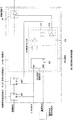
図1を参照して、第1実施形態のフェイルセーフ回路及び制御回路について説明する。図1は、第1実施形態の制御回路の概略構成図である。
(First embodiment)
A fail-safe circuit and a control circuit according to the first embodiment will be described with reference to FIG. FIG. 1 is a schematic configuration diagram of a control circuit according to the first embodiment.
制御回路10は、同期信号抽出回路20、タイミング信号生成回路22及びフェイルセーフ回路30を備えて構成されている。制御回路10には、画像信号、ピクセルクロック及び基準クロックが入力され、制御回路10は、タイミング信号を出力信号として出力する。出力信号として出力されるタイミング信号は、例えば、制御回路10の後段に設けられる画像表示装置(図示を省略する。)の走査線駆動回路で用いられる。
The
制御回路10に入力されたピクセルクロックは、3系統のピクセルクロックに3分岐され、それぞれ同期信号抽出回路20、タイミング信号生成回路22及びフェイルセーフ回路30に送られる。
The pixel clock input to the
同期信号抽出回路20は、クロック入力端子CKに入力されるピクセルクロックを用いて信号処理を行い、画像信号から同期信号を抽出する。抽出された同期信号は、タイミング信号生成回路22に送られる。 The synchronization signal extraction circuit 20 performs signal processing using the pixel clock input to the clock input terminal CK, and extracts the synchronization signal from the image signal. The extracted synchronization signal is sent to the timing signal generation circuit 22.
同期信号は、テレビ受像機など画像表示装置で画面を走査するタイミングを定めるのに用いられる信号である。同期信号には、水平同期信号と垂直同期信号がある。水平同期信号は、1つの走査線による水平方向の走査ごとにパルスを発生する。また、垂直同期信号は複数の水平方向の走査線による1画面の走査ごとにパルスを発生する。 The synchronization signal is a signal used to determine the timing for scanning the screen with an image display device such as a television receiver. The synchronization signal includes a horizontal synchronization signal and a vertical synchronization signal. The horizontal synchronization signal generates a pulse for each horizontal scan by one scan line. The vertical synchronizing signal generates a pulse every time one screen is scanned by a plurality of horizontal scanning lines.
図1では、同期信号の出力を1系統とした例を示しているが、この例に限定されない。例えば、出力を2系統以上として、水平同期信号と垂直同期信号とを別途に出力しても良いし、同種の同期信号を複数出力する構成としても良い。 Although FIG. 1 shows an example in which the output of the synchronization signal is one system, the present invention is not limited to this example. For example, the output may be two or more, and the horizontal synchronization signal and the vertical synchronization signal may be output separately, or a plurality of the same type of synchronization signals may be output.
タイミング信号生成回路22は、同期信号から、後段に設けられる走査線駆動回路の仕様に合わせて、タイミング信号を生成する。このとき、タイミング信号生成回路22は、クロック入力端子CKに入力されるピクセルクロックを用いて信号処理を行う。タイミング信号生成回路22で生成されたタイミング信号は、フェイルセーフ回路30に送られる。 The timing signal generation circuit 22 generates a timing signal from the synchronization signal in accordance with the specification of the scanning line driving circuit provided in the subsequent stage. At this time, the timing signal generation circuit 22 performs signal processing using the pixel clock input to the clock input terminal CK. The timing signal generated by the timing signal generation circuit 22 is sent to the fail safe circuit 30.
フェイルセーフ回路30は、判定部40と保護ゲート部90を備えて構成される。フェイルセーフ回路30に送られたタイミング信号は、保護ゲート部90に送られる。
The fail safe circuit 30 includes a determination unit 40 and a
保護ゲート部90は、判定部40で生成された判定信号をゲート信号として用いる。判定信号が、ピクセルクロックの入力が正常であることを示すとき、保護ゲート部90は、タイミング信号を通過させて、出力信号として出力する。一方、判定信号が、ピクセルクロックの入力が異常であることを示すとき、保護ゲート部90は、タイミング信号を遮断する。以下、判定信号の論理レベルが第1レベル(Lレベル)のとき、入力が異常であることを示し、また、第2レベル(Hレベル)のとき、入力が正常であることを示すものとして説明する。
The
保護ゲート部90は、判定信号の論理レベルに応じて出力の有無を制御する回路、例えば、タイミング信号と判定信号の論理積を出力するAND回路で構成することができる。
The
判定部40は、クロック判定回路200を備えて構成される。判定部40には、ピクセルクロックと基準クロックとが入力される。 The determination unit 40 includes a clock determination circuit 200. A pixel clock and a reference clock are input to the determination unit 40.
判定部40に入力されるピクセルクロックは、同期信号抽出回路20やタイミング信号生成回路22での信号処理に用いられるものと同じく画像信号に含まれるクロックである。一方、基準クロックは、ピクセルクロックとは独立したクロックであって、基準クロックとピクセルクロックは非同期である。 The pixel clock input to the determination unit 40 is a clock included in the image signal, similar to that used for signal processing in the synchronization signal extraction circuit 20 and the timing signal generation circuit 22. On the other hand, the reference clock is an independent clock from the pixel clock, and the reference clock and the pixel clock are asynchronous.
基準クロックは、一定の時間間隔でクロックパルスを有しており、任意好適な従来周知の水晶発振回路で構成される基準クロック発生手段24で生成することができる。なお、この基準クロックは、判定部40における判定の基準として用いられる。従って、ケーブル切断などによる基準クロックの入力異常を防ぐために、基準クロック発生手段24を、制御回路10に物理的に近い位置に設けるのが良い。また、基準クロック発生手段24を、制御回路10の内部に設ける構成としても良い。
The reference clock has clock pulses at a constant time interval, and can be generated by the reference clock generating means 24 configured by any suitable known crystal oscillation circuit. This reference clock is used as a determination reference in the determination unit 40. Therefore, it is preferable to provide the reference clock generating means 24 at a position physically close to the
クロック判定回路200は、基準クロックの計数値が定める期間内のピクセルクロックの計数値を用いて、ピクセルクロックの入力が正常であるか否かを判定する。クロック判定回路200は、この判定の結果を示すクロック判定信号を生成する。このクロック判定信号が、判定信号として判定部40から出力される。 The clock determination circuit 200 determines whether or not the input of the pixel clock is normal using the count value of the pixel clock within the period determined by the count value of the reference clock. The clock determination circuit 200 generates a clock determination signal indicating the result of this determination. This clock determination signal is output from the determination unit 40 as a determination signal.
(クロック判定回路の第1構成例)
図2を参照して、クロック判定回路の第1構成例について説明する。図2は、クロック判定回路の第1構成例の概略構成図である。
(First configuration example of clock determination circuit)
A first configuration example of the clock determination circuit will be described with reference to FIG. FIG. 2 is a schematic configuration diagram of a first configuration example of the clock determination circuit.
クロック判定回路200は、基準クロック計数部220、ピクセルクロック計数部230及びフリップフロップ回路240を備えて構成される。
The clock determination circuit 200 includes a reference clock counting unit 220, a pixel
クロック判定回路200に入力された基準クロックは2分岐される。2分岐された一方は基準クロック計数部220に送られ、他方は、フリップフロップ回路240に送られる。
The reference clock input to the clock determination circuit 200 is branched into two. One of the two branches is sent to the reference clock counter 220, and the other is sent to the flip-
基準クロック計数部220は、基準クロックを計数する。基準クロック計数部220は、計数結果である基準クロック計数値AQが予め設定した所定の値であるクリア値Mに等しいときに、クリア信号(CLEAR)の論理レベルをLレベルからHレベルに変化させて出力するとともに、基準クロック計数値AQを0にリセットする。また、基準クロック計数部220は、基準クロック計数値AQが予め設定した所定の値であるチェック値M−1に等しいときに、チェック信号(CHECK)の論理レベルをLレベルからHレベルに変化させて出力する。 The reference clock counting unit 220 counts the reference clock. The reference clock counting unit 220 changes the logic level of the clear signal (CLEAR) from the L level to the H level when the reference clock count value AQ, which is the counting result, is equal to the preset clear value M. And the reference clock count value AQ is reset to zero. Further, the reference clock counting unit 220 changes the logic level of the check signal (CHECK) from the L level to the H level when the reference clock count value AQ is equal to a predetermined check value M−1. Output.
基準クロック計数部220は、例えば、任意好適な従来周知のクロックカウンタ(以下、基準クロックカウンタと称する。)222とデコーダ224を備えて構成される。
The reference clock counting unit 220 includes, for example, any suitable and conventionally known clock counter (hereinafter referred to as a reference clock counter) 222 and a
基準クロックカウンタ222は、基準クロックの各クロックパルスの立ち上がりエッジごとに基準クロック計数値AQを1つずつ増加させ、基準クロック計数値AQを示す基準クロック計数信号を出力する。基準クロックカウンタ222は、基準クロック計数値AQがクリア値Mに等しくなると、基準クロック計数値AQを0にリセットする。 The reference clock counter 222 increases the reference clock count value AQ by one for each rising edge of each clock pulse of the reference clock, and outputs a reference clock count signal indicating the reference clock count value AQ. When the reference clock count value AQ becomes equal to the clear value M, the reference clock counter 222 resets the reference clock count value AQ to 0.
デコーダ224は、基準クロック計数信号が示す基準クロック計数値AQに対応して、チェック信号及びクリア信号を生成する。チェック信号は、基準クロック計数値AQがチェック値M−1に等しいときにHレベルとなり、それ以外はLレベルである。また、クリア信号は、基準クロック計数値AQがクリア値Mに等しいときにHレベルとなり、それ以外はLレベルである。
The
ピクセルクロック計数部230には、ピクセルクロックが入力され、ピクセルクロック計数部230は、ピクセルクロックを計数する。計数結果であるピクセルクロック計数値BQが予め設定した所定の値である停止値Nに等しいときに、コンパレータ信号をLレベルからHレベルに変化させて出力するとともに、計数動作を停止する。また、ピクセルクロック計数部230は、ピクセルクロック計数値BQが停止値N未満の値をとるとき、コンパレータ信号をLレベルとして、計数動作を行う。また、ピクセルクロック計数部230に入力されるクリア信号がHレベルになると、ピクセルクロック計数値BQが0にリセットされる。
A pixel clock is input to the pixel
ピクセルクロック計数部230は、例えば、ピクセルカウンタ232、ピクセルコンパレータ234、第1ピクセル定数器236及び第2ピクセル定数器238を備えて構成される。ピクセルカウンタ232は、イネーブル端子E及びロード端子LDを備える従来周知のクロックカウンタで構成できる。また、ピクセルコンパレータ234は、入力される2つの信号を比較して一致したときにHレベルの信号を出力し、不一致のときにLレベルの信号を出力する機能を有する、任意好適な回路で構成できる。また、第1ピクセル定数器236及び第2ピクセル定数器238は、予め設定された所定の値を保持しており、この保持している値を示す信号をピクセルカウンタ232あるいはピクセルコンパレータ234に送っている。
The pixel
ピクセルカウンタ232のロード端子LDには、基準クロック計数部220で生成されたクリア信号が入力される。ピクセルカウンタ232のロード端子LDに入力される信号の論理レベルがHレベルになると、第1ピクセル定数器236に保持されている値‘0’が、ピクセルカウンタ232に送られ、ピクセルクロック計数値BQが0にリセットされる。
The clear signal generated by the reference clock counter 220 is input to the load terminal LD of the pixel counter 232. When the logic level of the signal input to the load terminal LD of the pixel counter 232 becomes H level, the value '0' held in the first pixel
ピクセルカウンタ232は、ピクセルクロック計数値BQが0にリセットされた後、ロード端子LDに入力されるクリア信号の論理レベルがLレベルになるとピクセルクロックの計数を開始する。ピクセルカウンタ232は、ピクセルクロックに含まれるクロックパルスの立ち上がりエッジごとにピクセルクロック計数値BQを1つずつ増加させて、ピクセルクロック計数値BQを示すピクセルクロック計数信号を出力して、ピクセルコンパレータ234に送る。 After the pixel clock count value BQ is reset to 0, the pixel counter 232 starts counting the pixel clock when the logic level of the clear signal input to the load terminal LD becomes L level. The pixel counter 232 increments the pixel clock count value BQ by one for each rising edge of the clock pulse included in the pixel clock, and outputs a pixel clock count signal indicating the pixel clock count value BQ, to the pixel comparator 234. send.
ピクセルコンパレータ234は、第2ピクセル定数器238に保持されている停止値Nと、ピクセルクロック計数値BQとの比較を行う。ピクセルコンパレータ234は、ピクセルクロック計数値BQが停止値N以上のとき、コンパレータ信号の論理レベルをHレベルとして出力し、ピクセルクロック計数値BQが停止値N未満であるとき、コンパレータ信号の論理レベルをLレベルとする。
The pixel comparator 234 compares the stop value N held in the second pixel
また、このピクセルコンパレータ234の出力は、ピクセルカウンタ232のイネーブル端子Eに反転入力される。すなわち、コンパレータ信号の論理レベルがHレベルのとき、イネーブル端子Eから入力される信号の論理レベルがLレベルとなり、ピクセルカウンタ232は、ピクセルクロックの計数を停止する。一方、コンパレータ信号の論理レベルがLレベルのとき、イネーブル端子Eから入力される信号の論理レベルがHレベルとなり、ピクセルカウンタ232は、ピクセルクロックの計数を行う。 The output of the pixel comparator 234 is inverted and input to the enable terminal E of the pixel counter 232. That is, when the logic level of the comparator signal is H level, the logic level of the signal input from the enable terminal E becomes L level, and the pixel counter 232 stops counting the pixel clock. On the other hand, when the logic level of the comparator signal is L level, the logic level of the signal input from the enable terminal E becomes H level, and the pixel counter 232 counts the pixel clock.
ピクセルカウンタ232が、ピクセルクロックの計数を行った結果、ピクセルクロック計数値BQが停止値Nと等しくなると、コンパレータ信号の論理レベルがHレベルとなり、ピクセルクロックの計数が停止される。従って、ピクセルクロック計数値BQは停止値Nに維持され、コンパレータ信号もHレベルに維持される。 As a result of the pixel counter 232 counting the pixel clock, when the pixel clock count value BQ becomes equal to the stop value N, the logical level of the comparator signal becomes H level and the pixel clock count is stopped. Accordingly, the pixel clock count value BQ is maintained at the stop value N, and the comparator signal is also maintained at the H level.
フリップフロップ回路240では、入力端子Dにコンパレータ信号が入力され、イネーブル端子Eにチェック信号が入力される。また、フリップフロップ回路240のクロック端子CKには、基準クロックが入力される。
In the flip-
フリップフロップ回路240のイネーブル端子Eに入力されるチェック信号の論理レベルがHレベルになると、フリップフロップ回路240は、基準クロックのクロックパルスの立ち上がりエッジで、コンパレータ信号をデータとして取り込む。フリップフロップ回路240は、取り込んでいるコンパレータ信号を、クロック判定信号として出力する。
When the logic level of the check signal input to the enable terminal E of the flip-
(クロック判定回路の第1構成例の動作)
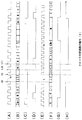
図3及び図4を参照して、クロック判定回路の第1構成例の動作を説明する。図3(A)〜(H)及び図4(A)〜(H)は、クロック判定回路の第1構成例の動作を説明するためのタイミングチャートである。図3(A)〜(H)は、ピクセルクロックの入力が正常に継続している場合を示し、図4(A)〜(H)は、ピクセルクロックの入力が停止する場合を示している。
(Operation of the first configuration example of the clock determination circuit)
The operation of the first configuration example of the clock determination circuit will be described with reference to FIGS. FIGS. 3A to 3H and FIGS. 4A to 4H are timing charts for explaining the operation of the first configuration example of the clock determination circuit. 3A to 3H show the case where the pixel clock input continues normally, and FIGS. 4A to 4H show the case where the pixel clock input stops.
図3(A)及び図4(A)は、基準クロックを示している。図3(B)及び図4(B)は、基準クロック計数信号を示している。図3(C)及び図4(C)は、チェック信号を示している。図3(D)及び図4(D)はクリア信号を示している。図3(E)及び図4(E)は、ピクセルクロックを示している。図3(F)及び図4(F)は、ピクセルクロック計数信号を示している。図3(G)及び図4(G)は、コンパレータ信号を示している。図3(H)及び図4(H)は、クロック判定信号を示している。 3A and 4A show the reference clock. 3B and 4B show the reference clock count signal. FIG. 3C and FIG. 4C show check signals. 3D and 4D show the clear signal. 3E and 4E show the pixel clock. 3 (F) and 4 (F) show the pixel clock count signal. 3 (G) and 4 (G) show the comparator signal. FIG. 3H and FIG. 4H show clock determination signals.
また、図3(A)〜(H)及び図4(A)〜(H)は、横軸に時間軸を取って示し、縦軸には、信号強度を論理レベルで示している。 In FIGS. 3A to 3H and FIGS. 4A to 4H, the horizontal axis indicates the time axis, and the vertical axis indicates the signal intensity as a logical level.
先ず、図3を参照して、ピクセルクロックの入力が正常である場合について説明する。 First, the case where the pixel clock input is normal will be described with reference to FIG.
同期信号抽出回路20、タイミング信号生成回路22、基準クロックカウンタ222、ピクセルカウンタ232及びフリップフロップ回路240は、リセット端子Rを有しており、電源投入時にリセットされる。この結果、チェック信号、クリア信号、コンパレータ信号及びクロック判定信号の論理レベルは、電源投入時にいずれもLレベルになるものとする。また、電源投入後は、基準クロック及びピクセルクロックがクロック判定回路200に継続的に入力されるものとして説明する。
The synchronization signal extraction circuit 20, the timing signal generation circuit 22, the reference clock counter 222, the pixel counter 232, and the flip-
時刻t0において、制御回路10が備える各回路に電源が投入される。電源投入された後、基準クロック及びピクセルクロックがクロック判定回路200に継続的に入力される。このとき、基準クロックカウンタ222は、基準クロックのクロックパルスを計数するので、基準クロック計数信号が示す基準クロック計数値AQは、基準クロックのクロックパルスの立ち上がりエッジごとに、1ずつ増加する。
At time t0, power is turned on to each circuit included in the
一方、ピクセルクロックカウンタ232は、計数を行わず、ピクセルクロック計数信号が示すピクセルクロック計数値BQは、0のままである。 On the other hand, the pixel clock counter 232 does not perform counting, and the pixel clock count value BQ indicated by the pixel clock count signal remains 0.
時刻t1において、基準クロック計数値AQがチェック値M−1に等しくなると、チェック信号の論理レベルはLレベルからHレベルに変化する。チェック信号の論理レベルがHレベルになると、フリップフロップ回路240は、次の基準クロックのクロックパルスの立ち上がり時(時刻t2)に、コンパレータ信号をデータ端子Dから取り込む。時刻t2では、コンパレータ信号はLレベルであるので、フリップフロップ回路240の出力信号であるクロック判定信号の論理レベルはLレベルとなる。
When the reference clock count value AQ becomes equal to the check value M-1 at time t1, the logic level of the check signal changes from the L level to the H level. When the logic level of the check signal becomes H level, the flip-
続いて時刻t2において、基準クロック計数値AQがクリア値Mに等しくなると、クリア信号の論理レベルはLレベルからHレベルに変化する。クリア信号の論理レベルがHレベルになると、ピクセルカウンタ232は、数値‘0’を第1ピクセル定数器236からロードする。このとき、チェック信号の論理レベルはHレベルからLレベルに変化する。
Subsequently, when the reference clock count value AQ becomes equal to the clear value M at time t2, the logic level of the clear signal changes from the L level to the H level. When the logic level of the clear signal becomes H level, the pixel counter 232 loads the numerical value “0” from the first pixel
その後、時刻t3において、クリア信号の論理レベルがHレベルからLレベルになった後、ピクセルカウンタ232は、ピクセルクロックの計数を開始する。また、時刻t2において、基準クロック計数値AQがクリア値Mに等しくなるので、時刻t3において、基準クロック計数値AQは0にリセットされる。 Thereafter, at time t3, after the logic level of the clear signal has changed from the H level to the L level, the pixel counter 232 starts counting the pixel clock. Further, since the reference clock count value AQ becomes equal to the clear value M at time t2, the reference clock count value AQ is reset to 0 at time t3.
時刻t4において、ピクセルクロック計数値BQが停止値Nに等しくなると、ピクセル計数部230は、コンパレータ信号の論理レベルをLレベルからHレベルに変化させるとともに、ピクセルクロックの計数を停止する。従って、ピクセルクロック計数値BQは停止値‘N’に等しい状態が続き、その間、コンパレータ信号の論理レベルはHレベルに維持される。 When the pixel clock count value BQ becomes equal to the stop value N at time t4, the pixel counter 230 changes the logical level of the comparator signal from the L level to the H level and stops counting the pixel clock. Accordingly, the pixel clock count value BQ continues to be equal to the stop value 'N', and during that time, the logic level of the comparator signal is maintained at the H level.
なお、ピクセルクロックの計数が停止している間も、基準クロックの計数は独立して行われている。 It should be noted that the reference clock is counted independently while the pixel clock counting is stopped.
時刻t5において、基準クロック計数値AQがチェック値M−1に等しくなると、チェック信号の論理レベルはLレベルからHレベルに変化する。チェック信号の論理レベルがHレベルになると、フリップフロップ回路240は、次の基準クロックのパルスの立ち上がり時(時刻t6)に、コンパレータ信号をデータ端子Dから取り込む。時刻t6では、コンパレータ信号はHレベルであるので、フリップフロップ回路240の出力信号であるクロック判定信号の論理レベルはHレベルになる。
When the reference clock count value AQ becomes equal to the check value M-1 at time t5, the logical level of the check signal changes from L level to H level. When the logic level of the check signal becomes H level, the flip-
続いて、時刻t6において、基準クロック計数値AQがクリア値Mに等しくなると、クリア信号の論理レベルはLレベルからHレベルに変化する。クリア信号の論理レベルがHレベルになると、ピクセルカウンタ232は、数値‘0’を第1ピクセル定数器236からロードする。時刻t7において、クリア信号の論理レベルがHレベルからLレベルになった後、ピクセルクロックカウンタ232は、ピクセルクロックの計数を再開する。
Subsequently, when the reference clock count value AQ becomes equal to the clear value M at time t6, the logic level of the clear signal changes from the L level to the H level. When the logic level of the clear signal becomes H level, the pixel counter 232 loads the numerical value “0” from the first pixel
また、時刻t6において基準クロック計数値AQがクリア値Mに等しくなるので、時刻t7において、基準クロック計数値AQは0にリセットされる。 Since the reference clock count value AQ becomes equal to the clear value M at time t6, the reference clock count value AQ is reset to 0 at time t7.
以後、時刻t3から時刻t7までと同様の動作が繰り返されるが、ピクセルクロックのクロックパルスがクロック判定回路200に継続して入力されている間、すなわちピクセルクロックの入力が正常状態にあるときは、フリップフロップ回路240においてデータを取り込む時刻において、コンパレータ信号がHレベルとなるので、クロック判定信号の論理レベルは、Hレベルに維持される。
Thereafter, the same operation is repeated from time t3 to time t7. However, while the clock pulse of the pixel clock is continuously input to the clock determination circuit 200, that is, when the input of the pixel clock is in a normal state, At the time when the flip-
次に、図4を参照して、ピクセルクロックの入力が停止した場合について説明する。 Next, a case where the input of the pixel clock is stopped will be described with reference to FIG.
時刻t8において、ピクセルクロックの入力が停止したものとする。この場合、ピクセルクロックの計数は中断するが、基準クロックは、ピクセルクロックから独立しているので、基準クロックの計数は継続する。 It is assumed that the input of the pixel clock is stopped at time t8. In this case, the counting of the pixel clock is interrupted, but the counting of the reference clock continues because the reference clock is independent of the pixel clock.
基準クロックの計数が継続した結果、時刻t10において、基準クロック計数値AQがチェック値M−1に等しくなると、チェック信号の論理レベルはLレベルからHレベルに変化する。チェック信号の論理レベルがHレベルになると、フリップフロップ回路240は、基準クロックに含まれるクロックパルスの次の立ち上がり時(時刻t11)で、コンパレータ信号をデータ端子Dから取り込む。
When the reference clock count value AQ becomes equal to the check value M-1 at time t10 as a result of continuing the reference clock counting, the logical level of the check signal changes from the L level to the H level. When the logic level of the check signal becomes H level, the flip-
時刻t9で、ピクセルクロックの入力が再開された場合であっても、ピクセルクロックの入力が一時停止したために、時刻t11の時点では、ピクセルクロック計数値BQは、停止した時間に対応して小さくなり、停止値N未満となる。従って、時刻t11おいて、フリップフロップ回路240がコンパレータ信号を取り込むときは、コンパレータ信号の論理レベルはLレベルとなっている。この結果、フリップフロップ回路240の出力信号であるクロック判定信号の論理レベルはLレベルとなる。
Even when the input of the pixel clock is resumed at time t9, the input of the pixel clock is temporarily stopped, so that at the time t11, the pixel clock count value BQ becomes smaller corresponding to the stopped time. The stop value is less than N. Accordingly, when the flip-
このように、ピクセルクロックの入力が停止する異常状態になると、クロック判定信号はLレベルになる。 In this way, when the pixel clock input is in an abnormal state that stops, the clock determination signal becomes L level.
また、時刻t11で、クリア信号の論理レベルがHレベルになると、ピクセルカウンタ232のピクセルクロック計数値BQが0にリセットされ、その後、図3を参照して説明したのと同様にピクセルカウンタ232の計数が正常に行われる。 Further, when the logic level of the clear signal becomes H level at time t11, the pixel clock count value BQ of the pixel counter 232 is reset to 0, and then the pixel counter 232 is reset in the same manner as described with reference to FIG. Counting is done normally.
以上説明したように、この構成によれば、ピクセルクロックの入力が継続している間、すなわち、ピクセルクロックの入力が正常状態であるときは、クロック判定信号の論理レベルはHレベルとなり、ピクセルクロックの入力に異常が発生すると、クロック判定信号の論理レベルはLレベルとなる。 As described above, according to this configuration, while the input of the pixel clock is continued, that is, when the input of the pixel clock is normal, the logic level of the clock determination signal becomes the H level, and the pixel clock When an abnormality occurs in the input of the clock, the logic level of the clock determination signal becomes L level.
この発明のフェイルセーフ回路及びこのフェイルセーフ回路を含む制御回路によれば、ピクセルクロックに対して独立している基準クロックを用いて、ピクセルクロックの入力が正常であるか否かを判定している。このため、ピクセルクロックが停止した場合であっても、これを検出し、タイミング信号の出力を停止することができる。 According to the fail-safe circuit of the present invention and the control circuit including the fail-safe circuit, it is determined whether or not the input of the pixel clock is normal using the reference clock independent of the pixel clock. . For this reason, even when the pixel clock is stopped, this can be detected and the output of the timing signal can be stopped.
また、この発明のフェイルセーフ回路及びこのフェイルセーフ回路を含む制御回路によれば、基準クロックが定める期間ごとにピクセルクロックの正常及び異常を判定するので、入力の正常又は異常に一意に対応したクロック判定信号が得られる。 Further, according to the fail-safe circuit of the present invention and the control circuit including the fail-safe circuit, the normality and abnormality of the pixel clock are determined every period determined by the reference clock, so that the clock uniquely corresponding to the normality or abnormality of the input A determination signal is obtained.
従って、クロック判定信号を判定信号として、タイミング信号生成回路22のイネーブル端子Eに送る構成にすることができる。このように構成すれば、判定信号が、ピクセルクロック入力の正常を示すときのみ、タイミング信号生成回路22を動作させ、判定信号が、ピクセルクロック入力の異常を示すときは、タイミング信号生成回路22をリセットすることができる。 Therefore, the clock determination signal can be sent to the enable terminal E of the timing signal generation circuit 22 as a determination signal. With this configuration, the timing signal generation circuit 22 is operated only when the determination signal indicates that the pixel clock input is normal, and when the determination signal indicates that the pixel clock input is abnormal, the timing signal generation circuit 22 is operated. Can be reset.
この結果、ピクセルクロックの入力の異常により、タイミング信号生成回路22の内部が不安定な状態になった場合であっても、タイミング信号生成回路22をリセットすることで、安定動作を再開させることができる。 As a result, even when the inside of the timing signal generation circuit 22 becomes unstable due to an abnormality in the input of the pixel clock, the stable operation can be resumed by resetting the timing signal generation circuit 22. it can.
(クロック判定回路の第2構成例)
図5を参照して、クロック判定回路の第2構成例について説明する。図5は、クロック判定回路の第2構成例の概略構成図である。
(Second configuration example of clock determination circuit)
A second configuration example of the clock determination circuit will be described with reference to FIG. FIG. 5 is a schematic configuration diagram of a second configuration example of the clock determination circuit.
このクロック判定回路201は、図2を参照して説明したクロック判定回路の第1構成例に加えて、クリア信号遅延器242及びコンパレータ信号遅延器244を備える点が異なっている。それ以外の構成は、第1構成例と同様なので、重複する説明を省略することもある。
The clock determination circuit 201 is different in that it includes a
クロック判定回路201に入力されたピクセルクロックは2分岐される。2分岐された一方は、ピクセルクロック計数部230に送られ、他方は、クリア信号遅延器242に送られる。
The pixel clock input to the clock determination circuit 201 is branched into two. One of the two branches is sent to the
クロック判定回路201に入力された基準クロックは3系統の基準クロックに分岐され、それぞれ、基準クロック計数部220、フリップフロップ回路240及びコンパレータ信号遅延器244に送られる。
The reference clock input to the clock determination circuit 201 is branched into three systems of reference clocks and sent to the reference clock counter 220, the flip-
クリア信号遅延器242は、基準クロック計数部220と、ピクセルクロック計数部230の間に設けられている。クリア信号遅延器242は、基準クロック計数部220で生成されたクリア信号を遅延させて、遅延クリア信号として、ピクセルクロック計数部230に送る。クリア信号遅延器242は、Dフリップフロップ回路として構成することができる。クリア信号遅延器242のクロック端子CKには、ピクセルクロックが入力される。クリア信号がHレベルになると、ピクセルクロックに含まれるクロックパルスの次の立ち上がりで、遅延クリア信号がHレベルになり、また、クリア信号がLレベルになると、ピクセルクロックに含まれるクロックパルスの次の立ち上がりで、遅延クリア信号がLレベルになる。
The clear
コンパレータ信号遅延器244は、ピクセルクロック計数部230と、フリップフロップ回路240の間に設けられている。コンパレータ信号遅延器244は、ピクセルクロック計数部230で生成されたコンパレータ信号を遅延させて、遅延コンパレータ信号としてフリップフロップ回路240に送る。コンパレータ信号遅延器244は、Dフリップフロップ回路として構成することができる。コンパレータ信号遅延器244のクロック端子CKには、基準クロックが入力される。コンパレータ信号がHレベルになると、基準クロックに含まれるクロックパルスの次の立ち上がりで、遅延コンパレータ信号がHレベルになり、また、コンパレータ信号がLレベルになると、基準クロックに含まれるクロックパルスの次の立ち上がりで、遅延コンパレータ信号がLレベルになる。
The comparator
クリア信号遅延器242及びコンパレータ信号遅延器244は、リセット端子を有しており、電源投入時にリセットされる。クリア信号遅延器242及びコンパレータ信号遅延器244の論理レベルは、電源投入時にいずれもLレベルになるものとする。
The clear
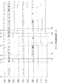
(クロック判定回路の第2構成例の動作)
図6及び図7を参照して、クロック判定回路の第2構成例の動作を説明する。図6(A)〜(J)及び図7(A)〜(J)は、クロック判定回路の第2構成例の動作を説明するためのタイミングチャートである。図6(A)〜(J)は、ピクセルクロックの入力が正常に継続している場合を示し、図7(A)〜(J)は、ピクセルクロックの入力が停止する場合を示している。
(Operation of Second Configuration Example of Clock Determination Circuit)
The operation of the second configuration example of the clock determination circuit will be described with reference to FIGS. 6A to 6J and FIGS. 7A to 7J are timing charts for explaining the operation of the second configuration example of the clock determination circuit. 6A to 6J show a case where the pixel clock input continues normally, and FIGS. 7A to 7J show a case where the pixel clock input stops.
図6(A)及び図7(A)は、基準クロックを示している。図6(B)及び図7(B)は、基準クロック計数信号を示している。図6(C)及び図7(C)は、チェック信号を示している。図6(D)及び図7(D)はクリア信号を示している。図6(E)及び図7(E)は、ピクセルクロックを示している。図6(F)及び図7(F)は、遅延クリア信号を示している。図6(G)及び図7(G)は、ピクセルクロック計数信号を示している。図6(H)及び図7(H)は、コンパレータ信号を示している。図6(I)及び図7(I)は、遅延コンパレータ信号を示している。図6(J)及び図7(J)は、クロック判定信号を示している。 6A and 7A show the reference clock. FIG. 6B and FIG. 7B show the reference clock count signal. FIG. 6C and FIG. 7C show check signals. 6D and 7D show the clear signal. 6E and 7E show the pixel clock. FIGS. 6F and 7F show delayed clear signals. FIG. 6G and FIG. 7G show pixel clock count signals. FIGS. 6H and 7H show the comparator signals. 6 (I) and 7 (I) show the delayed comparator signal. FIG. 6J and FIG. 7J show clock determination signals.
また、図6(A)〜(J)及び図7(A)〜(J)は、横軸に時間軸を取って示し、縦軸には、信号強度を論理レベルで示している。 In FIGS. 6A to 6J and FIGS. 7A to 7J, the horizontal axis indicates the time axis, and the vertical axis indicates the signal intensity at a logical level.
なお、基準クロック、基準クロック計数信号、チェック信号、クリア信号、ピクセルクロックについては、クロック判定回路の第1構成例における動作と同様なので、重複する説明を省略することもある。 The reference clock, the reference clock count signal, the check signal, the clear signal, and the pixel clock are the same as those in the first configuration example of the clock determination circuit, and thus redundant description may be omitted.
先ず、図6を参照して、ピクセルクロックの入力が正常である場合について説明する。 First, the case where the pixel clock input is normal will be described with reference to FIG.
時刻t0において、制御回路10が備える各回路に電源が投入される。電源投入された後、基準クロック及びピクセルクロックがクロック判定回路201に継続的に入力される。このとき、基準クロックカウンタ222は、基準クロックのクロックパルスを計数するので、基準クロック計数信号が示す基準クロック計数値AQは、基準クロックのクロックパルスの立ち上がりエッジごとに、1ずつ増加する。
At time t0, power is turned on to each circuit included in the
一方、ピクセルクロックカウンタ232は、計数を行わず、ピクセルクロック計数信号が示すピクセルクロック計数値BQは、0のままである。 On the other hand, the pixel clock counter 232 does not perform counting, and the pixel clock count value BQ indicated by the pixel clock count signal remains 0.
時刻t1において、基準クロック計数値AQがチェック値M−1に等しくなると、チェック信号の論理レベルはLレベルからHレベルに変化する。チェック信号の論理レベルがHレベルになると、フリップフロップ回路240は、基準クロックに含まれるクロックパルスの次の立ち上がり時(時刻t2)に、遅延コンパレータ信号をデータ端子Dから取り込む。時刻t2では、遅延コンパレータ信号はLレベルであるので、フリップフロップ回路240の出力信号であるクロック判定信号の論理レベルはLレベルとなる。
When the reference clock count value AQ becomes equal to the check value M-1 at time t1, the logic level of the check signal changes from the L level to the H level. When the logic level of the check signal becomes H level, the flip-
続いて時刻t2において、基準クロック計数値AQがクリア値Mに等しくなると、クリア信号の論理レベルはLレベルからHレベルに変化する。クリア信号の論理レベルがHレベルになると、クリア信号遅延器242は、入力されたクリア信号を遅延させて、ピクセルクロックのクロックパルスの次の立ち上がり時(時刻t21)に、遅延クリア信号として出力する。このとき、チェック信号の論理レベルはHレベルからLレベルに変化する。また、時刻t2において、基準クロック計数値AQがクリア値Mに等しくなるので、時刻t3において、基準クロック計数値AQは0にリセットされる。
Subsequently, when the reference clock count value AQ becomes equal to the clear value M at time t2, the logic level of the clear signal changes from the L level to the H level. When the logic level of the clear signal becomes H level, the clear
時刻t21において、遅延クリア信号の論理レベルがHレベルになると、ピクセルカウンタ232は、数値‘0’を、第1ピクセル定数器236からロードする。
When the logic level of the delayed clear signal becomes H level at time t 21, the pixel counter 232 loads the numerical value “0” from the first pixel
時刻t22において、遅延クリア信号の論理レベルがLレベルになった後、ピクセルカウンタ232は、ピクセルクロックの計数を開始する。 At time t22, after the logic level of the delayed clear signal becomes L level, the pixel counter 232 starts counting the pixel clock.
時刻t4において、ピクセルクロック計数値BQが停止値Nに等しくなると、ピクセルクロック計数部230は、コンパレータ信号の論理レベルをLレベルからHレベルに変化させるとともに、ピクセルクロックの計数を停止する。従って、ピクセルクロック計数値BQは停止値‘N’に等しい状態が続き、その間、コンパレータ信号の論理レベルはHレベルに維持される。
When the pixel clock count value BQ becomes equal to the stop value N at time t4, the pixel
時刻t4において、コンパレータ信号の論理レベルがHレベルになると、コンパレータ信号遅延器244は、基準クロックに含まれるクロックパルスの次の立ち上がり時(時刻t23)に、コンパレータ遅延信号をLレベルからHレベルに変化させて出力する。
When the logic level of the comparator signal becomes H level at time t4, the comparator
なお、ピクセルクロックの計数が停止している間も、基準クロックの計数は独立して行われている。 It should be noted that the reference clock is counted independently while the pixel clock counting is stopped.
時刻t5において、基準クロック計数値AQがチェック値M−1に等しくなると、チェック信号の論理レベルがLレベルからHレベルに変化する。チェック信号の論理レベルがHレベルになると、フリップフロップ回路240は、次の基準クロックのクロックパルスの立ち上がり時(時刻t6)に、遅延コンパレータ信号をデータ端子Dから取り込む。時刻t6では、遅延コンパレータ信号はHレベルであるので、フリップフロップ回路240の出力信号であるクロック判定信号の論理レベルはHレベルとなる。
When the reference clock count value AQ becomes equal to the check value M-1 at time t5, the logical level of the check signal changes from the L level to the H level. When the logic level of the check signal becomes H level, the flip-
また、時刻t24において、遅延クリア信号の論理レベルがHレベルになると、ピクセルカウンタ232は、数値‘0’を第1ピクセル定数器236からロードする。時刻t25において、遅延クリア信号の論理レベルがHレベルからLレベルになった後、ピクセルクロックカウンタ232は、ピクセルクロックの計数を開始する。
At time t24, when the logic level of the delayed clear signal becomes H level, the pixel counter 232 loads the numerical value “0” from the first pixel
また、時刻t6において、基準クロック計数値AQがクリア値Mに等しくなるので、時刻t7において、基準クロック計数値AQは0にリセットされる。 Further, since the reference clock count value AQ becomes equal to the clear value M at time t6, the reference clock count value AQ is reset to 0 at time t7.
以後、時刻t3から時刻t7までの動作を繰り返すが、ピクセルクロックのクロックパルスが継続してクロック判定回路に入力されている間、すなわちピクセルクロックが正常状態にあるときは、フリップフロップ回路240においてデータを取り込む時刻において、遅延コンパレータ信号がHレベルとなるので、クロック判定信号の論理レベルは、Hレベルに維持される。
Thereafter, the operation from time t3 to time t7 is repeated. While the clock pulse of the pixel clock is continuously input to the clock determination circuit, that is, when the pixel clock is in a normal state, the data in the flip-
次に、図7を参照して、ピクセルクロックの入力が停止した場合について説明する。 Next, a case where the input of the pixel clock is stopped will be described with reference to FIG.
時刻t8において、ピクセルクロックの入力が停止したものとする。この場合、ピクセルクロックの計数は中断するが、基準クロックは、ピクセルクロックから独立しているので、基準クロックの計数は継続する。 It is assumed that the input of the pixel clock is stopped at time t8. In this case, the counting of the pixel clock is interrupted, but the counting of the reference clock continues because the reference clock is independent of the pixel clock.
基準クロックの計数が継続して、時刻t10において、基準クロック計数値AQがチェック値M−1に等しくなると、チェック信号の論理レベルはLレベルからHレベルに変化する。チェック信号の論理レベルがHレベルになると、フリップフロップ回路240は、基準クロックに含まれるクロックパルスの次の立ち上がり時(時刻t11)に、遅延コンパレータ信号をデータ端子Dから取り込む。
When the reference clock count continues and the reference clock count value AQ becomes equal to the check value M-1 at time t10, the logic level of the check signal changes from the L level to the H level. When the logic level of the check signal becomes H level, the flip-
時刻t9で、ピクセルクロックの入力が再開された場合であっても、ピクセルクロックの入力が一時停止したために、時刻t11の時点では、ピクセルクロックの計数値BQは、停止した時間に対応して小さくなり停止値N未満となる。従って、時刻t11においてフリップフロップ回路240が遅延コンパレータ信号を取り込むとき、遅延コンパレータ信号の論理レベルはLレベルとなる。この結果、フリップフロップ回路240の出力信号であるクロック判定信号の論理レベルはLレベルとなる。
Even when the input of the pixel clock is resumed at time t9, the pixel clock count value BQ becomes small corresponding to the stopped time at the time t11 because the input of the pixel clock is temporarily stopped. Therefore, the stop value is less than N. Therefore, when the flip-
このように、ピクセルクロックの入力が停止する異常状態になると、クロック判定信号はLレベルになる。 In this way, when the pixel clock input is in an abnormal state that stops, the clock determination signal becomes L level.
また、時刻t26で、遅延クリア信号の論理レベルがHレベルになると、ピクセルカウンタ232が0にリセットされ、その後、図6を参照して説明したのと同様にピクセルカウンタ232の計数が正常に行われる。 Further, when the logic level of the delayed clear signal becomes H level at time t26, the pixel counter 232 is reset to 0, and thereafter the pixel counter 232 performs normal counting as described with reference to FIG. Is called.
以上説明したクロック判定回路の第2構成例によれば、クロック判定回路の第1構成例で得られる効果に加えて、以下の効果が得られる。すなわち、クロック判定回路の第2構成例は、クリア信号に対して、ピクセルクロックの1周期分遅延させて、ピクセルクロックカウンタをリセットし、またコンパレータ出力信号をピクセルクロックの1周期分遅延させている。この結果、コンパレータ出力信号が変化する時刻が、コンパレータ出力信号が変化する時刻と、基準クロックに含まれる立ち上がりエッジの時刻との差が大きくなり、フリップフロップ回路がメタステーブル状態に入るのを確実に防ぐことができる。 According to the second configuration example of the clock determination circuit described above, in addition to the effects obtained in the first configuration example of the clock determination circuit, the following effects can be obtained. That is, the second configuration example of the clock determination circuit delays the pixel signal by one cycle of the pixel clock with respect to the clear signal, resets the pixel clock counter, and delays the comparator output signal by one cycle of the pixel clock. . As a result, the time at which the comparator output signal changes increases the difference between the time at which the comparator output signal changes and the time of the rising edge included in the reference clock, ensuring that the flip-flop circuit enters the metastable state. Can be prevented.
(第1実施形態の制御回路の他の構成例)
図1では、クロック判定回路が1系統の判定信号を出力し、その後分岐して、タイミング信号生成回路20と保護ゲート部90に送る構成例を示しているが、これに限定されるものではない。
(Another configuration example of the control circuit of the first embodiment)
Although FIG. 1 shows a configuration example in which the clock determination circuit outputs a determination signal of one system and then branches and sends it to the timing signal generation circuit 20 and the
図8は、第1変形例の制御回路の概略構成図である。この制御回路11では、フェイルセーフ回路31の判定部41が、出力ゲート部300を備えている。出力ゲート部300において、クロック判定信号を2分岐した後、一方をタイミング信号生成回路22に送り、他方を保護ゲート部90に送る。このとき、判定信号が、増幅回路302及び304により適宜増幅される構成にしても良い。
FIG. 8 is a schematic configuration diagram of a control circuit of a first modification. In the
図9は、第2変形例の制御回路の概略構成図である。この制御回路12では、フェイルセーフ回路32の判定部42が、出力ゲート部310を備えている。出力ゲート部310において、クロック判定信号が2分岐される。出力ゲート部310は、テスト端子316及びOR回路312を備えている。
FIG. 9 is a schematic configuration diagram of a control circuit of a second modification. In the
OR回路312には、クロック判定信号の2分岐された一方と、テスト端子316を経て入力されたテスト信号が増幅回路318で適宜増幅されて入力される。OR回路312の出力である論理和信号は、判定信号としてタイミング信号生成回路22に送られる。また、クロック判定信号の2分岐された他方は、必要に応じて増幅器314で適宜増幅されて、判定信号として保護ゲート部90に送られる。
The OR
この構成によれば、例えば、テスト端子316にHレベルの信号を入力すると、クロック判定信号の論理レベルによらず、OR回路312の出力がHレベルになる。この結果、タイミング信号生成回路22のイネーブル端子Eに入力される判定信号の論理レベルは、常にHレベルとなるので、ピクセルクロックの入力に異常が発生した場合であっても、タイミング信号生成回路22はリセットされない。このことを利用すれば、ピクセルクロックの入力異常時のタイミング信号生成回路22の振る舞いを容易に確認することができる。
According to this configuration, for example, when an H level signal is input to the test terminal 316, the output of the
図10は、第3変形例の制御回路を示す図である。この制御回路13では、フェイルセーフ回路33の判定部43は、出力ゲート部320を備えている。出力ゲート部320において、クロック判定信号が第1〜3のクロック判定信号に3分岐される。保護ゲート部91は、第1のゲート回路としてANDゲート94を備え、第2のゲート回路としてORゲート96を備えている。
FIG. 10 is a diagram illustrating a control circuit of a third modification. In the control circuit 13, the determination unit 43 of the failsafe circuit 33 includes an
また、タイミング信号生成回路22では、2系統のタイミング信号が生成されている。一方のタイミング信号はANDゲート94に送られ、他方のタイミング信号はORゲート96に送られる。
The timing signal generation circuit 22 generates two systems of timing signals. One timing signal is sent to the AND
第1のクロック判定信号は、必要に応じて増幅回路322で適宜増幅されて、正論理のまま、第1判定信号としてタイミング信号生成回路22に送られる。
The first clock determination signal is appropriately amplified by the
第2のクロック判定信号は、必要に応じて増幅回路324で適宜増幅されて、正論理のまま、第2判定信号として、保護ゲート部91のANDゲート94に送られる。このANDゲート94における第2判定信号を用いた処理は、第1実施形態と同様である。
The second clock determination signal is appropriately amplified by the
第3のクロック判定信号は、反転回路326で負論理に反転された後、第3判定信号として、保護ゲート部91のORゲート96に送られる。すなわち、保護ゲート部91のORゲート96に送られる第3判定信号の論理レベルは、ピクセルクロックの入力が正常であるときはLレベルとなり、ピクセルクロックの入力に異常が発生したときはHレベルとなる。
The third clock determination signal is inverted to negative logic by the inverting
ORゲート96からの出力信号は、ピクセルクロックが正常であるときは、タイミング信号をそのまま出力し、ピクセルクロックが異常であるときは、論理レベルがHレベルの信号を出力する。
The output signal from the
従って、後段に設けられる走査線駆動回路において、ORゲート96からの出力信号であるタイミング信号を用いることで、走査線駆動回路における誤動作を効果的に防止することができる。
Therefore, by using a timing signal that is an output signal from the
(第2実施形態)
図11を参照して第2実施形態のフェイルセーフ回路及び制御回路について説明する。図11は、第2実施形態の制御回路の概略構成図である。
(Second Embodiment)
A fail-safe circuit and a control circuit according to the second embodiment will be described with reference to FIG. FIG. 11 is a schematic configuration diagram of a control circuit according to the second embodiment.
この制御回路14では、フェイルセーフ回路34の判定部44が動作判定回路400を備えている点が第1実施形態と異なっており、それ以外の点には、第1実施形態と同様であるので、重複する説明を省略することもある。 The control circuit 14 is different from the first embodiment in that the determination unit 44 of the fail-safe circuit 34 includes an operation determination circuit 400, and is otherwise the same as the first embodiment. In some cases, duplicate descriptions are omitted.
制御回路14は、同期信号抽出回路20、タイミング信号生成回路22及びフェイルセーフ回路34を備えて構成されている。制御回路14には、画像信号、ピクセルクロック及び基準クロックが入力され、制御回路14は、タイミング信号を出力信号として出力する。出力信号として出力されるタイミング信号は、例えば、制御回路14の後段に設けられる画像表示装置(図示を省略する。)の走査線駆動回路で用いられる。 The control circuit 14 includes a synchronization signal extraction circuit 20, a timing signal generation circuit 22, and a fail safe circuit 34. An image signal, a pixel clock, and a reference clock are input to the control circuit 14, and the control circuit 14 outputs a timing signal as an output signal. The timing signal output as the output signal is used, for example, in a scanning line driving circuit of an image display device (not shown) provided in the subsequent stage of the control circuit 14.
制御回路14に入力されたピクセルクロックは、3系統のピクセルクロックに3分岐され、それぞれ同期信号抽出回路20、タイミング信号生成回路22及びフェイルセーフ回路34に送られる。 The pixel clock input to the control circuit 14 is branched into three pixel clocks and sent to the synchronization signal extraction circuit 20, the timing signal generation circuit 22, and the fail safe circuit 34, respectively.
同期信号抽出回路20は、クロック入力端子CKに入力されるピクセルクロックを用いて信号処理を行い、画像信号から同期信号を抽出する。抽出された同期信号は、タイミング信号生成回路22に送られる。 The synchronization signal extraction circuit 20 performs signal processing using the pixel clock input to the clock input terminal CK, and extracts the synchronization signal from the image signal. The extracted synchronization signal is sent to the timing signal generation circuit 22.
タイミング信号生成回路22は、同期信号から、後段に設けられる走査線駆動回路の仕様に合わせて、タイミング信号を生成する。このとき、タイミング信号生成回路22は、クロック入力端子CKに入力されるピクセルクロックを用いて信号処理を行う。タイミング信号生成回路22で生成されたタイミング信号は、フェイルセーフ回路34に送られる。 The timing signal generation circuit 22 generates a timing signal from the synchronization signal in accordance with the specification of the scanning line driving circuit provided in the subsequent stage. At this time, the timing signal generation circuit 22 performs signal processing using the pixel clock input to the clock input terminal CK. The timing signal generated by the timing signal generation circuit 22 is sent to the fail safe circuit 34.
フェイルセーフ回路34は、判定部44と保護ゲート部90を備えて構成される。フェイルセーフ回路34に送られたタイミング信号は、2分岐される。2分岐されたタイミング信号の一方は、保護ゲート部90に送られ、他方は、判定部44に送られる。
The fail safe circuit 34 includes a determination unit 44 and a
保護ゲート部90は、判定部44で生成された判定信号をゲート信号として用いる。判定信号が、ピクセルクロックの入力が正常であることを示すとき、保護ゲート部90は、タイミング信号を通過させて、出力信号として出力する。一方、判定信号が、ピクセルクロックの入力が異常であることを示すとき、保護ゲート部90は、タイミング信号を遮断する。
The
判定部44は、クロック判定回路200と動作判定回路400を備えて構成される。判定部44には、タイミング信号、ピクセルクロック及び基準クロックが入力される。判定部44に入力されたピクセルクロックは2分岐され、一方がクロック判定回路200に送られ、他方が動作判定回路400に送られる。 The determination unit 44 includes a clock determination circuit 200 and an operation determination circuit 400. The determination unit 44 receives a timing signal, a pixel clock, and a reference clock. The pixel clock input to the determination unit 44 is branched into two, one being sent to the clock determination circuit 200 and the other being sent to the operation determination circuit 400.
クロック判定回路200は、図1を参照して説明したのと同様に、基準クロックの計数値が定める期間内のピクセルクロックの計数値を用いて、ピクセルクロックの入力が正常であるか否かを判定する。クロック判定回路200は、この判定の結果を示すクロック判定信号を生成する。 As described with reference to FIG. 1, the clock determination circuit 200 uses the pixel clock count value within the period determined by the reference clock count value to determine whether or not the pixel clock input is normal. judge. The clock determination circuit 200 generates a clock determination signal indicating the result of this determination.
動作判定回路400は、例えば、カウンタ404、デコーダ406及びANDゲート408を備えて構成される。カウンタ404の出力が0から所定の値Tまでの間、デコーダ406は、論理レベルがHレベルである信号を出力し、それ以外の間はLレベルの信号を出力する。
The operation determination circuit 400 includes, for example, a counter 404, a decoder 406, and an AND
ANDゲート408には、タイミング信号と、デコーダ406の出力であるデコーダ出力信号が入力される。ANDゲート408は、タイミング信号とデコーダ出力信号がともにHレベルであるとき、タイミング信号が正常であることを示す動作判定信号を生成する。
A timing signal and a decoder output signal that is an output of the decoder 406 are input to the AND
すなわち、動作判定回路400は、ピクセルクロックが定める期間内であって、タイミング信号に含まれるスタートパルスが持続している期間内には、タイミング信号が正常であることを示す動作判定信号を出力する。 That is, the operation determination circuit 400 outputs an operation determination signal indicating that the timing signal is normal within a period determined by the pixel clock and within a period in which the start pulse included in the timing signal is sustained. .
動作判定信号と、クロック判定部200で生成されたクロック判定信号とは、ANDゲート402に入力され、動作判定信号とクロック判定信号の論理積(AND)が判定信号として出力される。
The operation determination signal and the clock determination signal generated by the clock determination unit 200 are input to the AND
なお、例えば、保護ゲート部90を、タイミング信号、動作判定信号及びクロック判定信号が入力される3入力のANDゲートとして構成し、また、タイミング信号生成回路22のイネーブル端子Eを、動作判定信号及びクロック判定信号が入力される2入力のANDゲートとして構成して、判定部44からは、動作判定信号とクロック判定信号をそれぞれ出力する構成にしても良い。
For example, the
(第3実施形態)
図12を参照して第3実施形態の制御回路について説明する。図12は、第3実施形態の制御回路を説明するための概略構成図である。
(Third embodiment)
The control circuit of the third embodiment will be described with reference to FIG. FIG. 12 is a schematic configuration diagram for explaining a control circuit of the third embodiment.
第3実施形態の制御回路15では、フェイルセーフ回路35の判定部45が、さらに第1同期判定回路410と第2同期判定回路420を備えている点が第1実施形態の制御回路と異なっており、それ以外の点には、第1実施形態と同様であるので、重複する説明を省略することもある。 The control circuit 15 of the third embodiment differs from the control circuit of the first embodiment in that the determination unit 45 of the fail-safe circuit 35 further includes a first synchronization determination circuit 410 and a second synchronization determination circuit 420. Since the other points are the same as those in the first embodiment, a duplicate description may be omitted.
制御回路15は、同期信号抽出回路20、タイミング信号生成回路22及びフェイルセーフ回路35を備えて構成されている。制御回路15には、2系統の画像信号、ピクセルクロック及び基準クロックが入力され、制御回路15は、タイミング信号を2系統の出力信号として出力する。出力信号として出力されるタイミング信号は、例えば、制御回路15の後段に設けられる画像表示装置の走査線駆動回路で用いられる。 The control circuit 15 includes a synchronization signal extraction circuit 20, a timing signal generation circuit 22, and a fail safe circuit 35. The control circuit 15 receives two systems of image signals, a pixel clock, and a reference clock, and the control circuit 15 outputs a timing signal as two systems of output signals. The timing signal output as the output signal is used, for example, in the scanning line driving circuit of the image display device provided in the subsequent stage of the control circuit 15.
制御回路15に入力されたピクセルクロックは、3系統のピクセルクロックに3分岐され、それぞれ同期信号抽出回路20、タイミング信号生成回路22及びフェイルセーフ回路35に送られる。 The pixel clock input to the control circuit 15 is branched into three pixel clocks and sent to the synchronization signal extraction circuit 20, the timing signal generation circuit 22, and the fail safe circuit 35, respectively.
同期信号抽出回路20は、クロック入力端子CKに入力されるピクセルクロックを用いて信号処理を行い、2系統の画像信号からそれぞれ同期信号を抽出する。ここでは一方を、例えば水平同期信号(第1同期信号と称することもある。)とし、他方を、例えば垂直同期信号(第2同期信号と称することもある。)とする。 The synchronization signal extraction circuit 20 performs signal processing using the pixel clock input to the clock input terminal CK, and extracts synchronization signals from the two systems of image signals. Here, for example, one is a horizontal synchronizing signal (sometimes referred to as a first synchronizing signal), and the other is a vertical synchronizing signal (sometimes referred to as a second synchronizing signal).
第1同期信号及び第2同期信号は、それぞれ2分岐される。2分岐された一方は、タイミング信号生成回路22に送られ、他方は、フェイルセーフ回路35に送られる。 Each of the first synchronization signal and the second synchronization signal is branched into two. One of the two branches is sent to the timing signal generation circuit 22, and the other is sent to the fail safe circuit 35.
タイミング信号生成回路22は、第1同期信号及び第2同期信号から、後段に設けられる走査線駆動回路の仕様に合わせて、第1タイミング信号及び第2タイミング信号を生成する。このとき、タイミング信号生成回路22は、クロック入力端子CKに入力されるピクセルクロックを用いて信号処理を行う。タイミング信号生成回路22で生成された第1タイミング信号及び第2タイミング信号は、フェイルセーフ回路35に送られる。 The timing signal generation circuit 22 generates a first timing signal and a second timing signal from the first synchronization signal and the second synchronization signal in accordance with the specifications of the scanning line driving circuit provided in the subsequent stage. At this time, the timing signal generation circuit 22 performs signal processing using the pixel clock input to the clock input terminal CK. The first timing signal and the second timing signal generated by the timing signal generation circuit 22 are sent to the fail safe circuit 35.
フェイルセーフ回路35は、判定部45と保護ゲート部92を備えて構成される。フェイルセーフ回路35に送られた第1タイミング信号及び第2タイミング信号は、保護ゲート部92に送られる。 The fail safe circuit 35 includes a determination unit 45 and a protection gate unit 92. The first timing signal and the second timing signal sent to the fail safe circuit 35 are sent to the protection gate unit 92.
保護ゲート部92は、第1保護ゲート回路97及び第2保護ゲート回路98を備えている。第1保護ゲート回路97及び第2保護ゲート回路98は、判定部45で生成された判定信号をそれぞれゲート信号として用いる。第1保護ゲート回路97及び第2保護ゲート回路98は、判定信号の論理レベルに応じて出力の有無を制御するAND回路で構成することができる。
The protection gate unit 92 includes a first
判定信号が、ピクセルクロックの入力が正常であることを示すとき、第1保護ゲート回路97は、第1タイミング信号を通過させて、出力信号として出力する。一方、判定信号が、ピクセルクロックの入力が異常であることを示すとき、第1保護ゲート回路97は、第1タイミング信号を遮断する。
When the determination signal indicates that the input of the pixel clock is normal, the first
同様に、判定信号が、ピクセルクロックの入力が正常であることを示すとき、第2保護ゲート回路98は、第2タイミング信号を通過させて、出力信号として出力する。一方、判定信号が、ピクセルクロックの入力が異常であることを示すとき、第2保護ゲート回路98は、第1タイミング信号を遮断する。
Similarly, when the determination signal indicates that the input of the pixel clock is normal, the second
判定部45は、クロック判定回路200、第1同期判定回路410及び第2同期判定回路420を備えて構成される。 The determination unit 45 includes a clock determination circuit 200, a first synchronization determination circuit 410, and a second synchronization determination circuit 420.
判定部45に入力された第1同期信号は、第1同期判定回路410に送られる。 The first synchronization signal input to the determination unit 45 is sent to the first synchronization determination circuit 410.
判定部45に入力された第2同期信号は2分岐される。2分岐された一方は第1同期判定回路410に送られ、他方は第2同期判定回路420に送られる。 The second synchronization signal input to the determination unit 45 is branched into two. One of the two branches is sent to the first synchronization determination circuit 410 and the other is sent to the second synchronization determination circuit 420.
判定部45に入力された基準クロックは2分岐される。2分岐された一方はクロック判定回路200に送られ、他方は、第2同期判定回路420に送られる。 The reference clock input to the determination unit 45 is branched into two. One of the two branches is sent to the clock determination circuit 200, and the other is sent to the second synchronization determination circuit 420.
クロック判定回路200は、基準クロックの計数値が定める期間内のピクセルクロックの計数値を用いて、ピクセルクロックの入力が正常であるか否かを判定する。クロック判定回路200は、この判定の結果を示すクロック判定信号を生成する。 The clock determination circuit 200 determines whether or not the input of the pixel clock is normal using the count value of the pixel clock within the period determined by the count value of the reference clock. The clock determination circuit 200 generates a clock determination signal indicating the result of this determination.
第1同期判定回路410は、第2同期信号の計数値が定める期間内の第1同期信号の計数値を用いて、第1同期信号が正常であるか否かを判定する。第1同期判定回路410は、この判定の結果を示す第1同期判定信号を生成する。 The first synchronization determination circuit 410 determines whether or not the first synchronization signal is normal using the count value of the first synchronization signal within the period determined by the count value of the second synchronization signal. The first synchronization determination circuit 410 generates a first synchronization determination signal indicating the result of this determination.
第2同期判定回路420は、基準クロックの計数値が定める期間内の第2同期信号の計数値を用いて、第2同期信号が正常であるか否かを判定する。第2同期判定回路420は、この判定の結果を示す第2同期判定信号を生成する。 The second synchronization determination circuit 420 determines whether or not the second synchronization signal is normal using the count value of the second synchronization signal within the period determined by the count value of the reference clock. The second synchronization determination circuit 420 generates a second synchronization determination signal indicating the result of this determination.
クロック判定信号、第1同期判定信号及び第2同期判定信号は、ANDゲート430に入力され、その論理積(AND)が判定信号として出力される。
The clock determination signal, the first synchronization determination signal, and the second synchronization determination signal are input to the AND
クロック判定回路200、第1同期判定回路410及び第2同期判定回路420は、同様の判定回路として構成することができる。 The clock determination circuit 200, the first synchronization determination circuit 410, and the second synchronization determination circuit 420 can be configured as similar determination circuits.
これらの判定回路は、第1クロック計数部と、第2クロック計数部と、フリップフロップ回路とを備えて構成される。 These determination circuits include a first clock counting unit, a second clock counting unit, and a flip-flop circuit.
第1クロック計数部は、入力される第1クロックを計数して、計数結果である第1クロック計数値が予め設定されているクリア値Mに等しくなると、クリア信号をLレベルからHレベルに変化させるとともに、第1クロック計数値を0にリセットする。また、第1クロック計数部は、第1クロック計数値が予め設定されているチェック値M−1に等しいときにチェック信号をLレベルからHレベルに変化させる。 The first clock counting unit counts the first clock input, and when the first clock count value, which is the counting result, becomes equal to the preset clear value M, the clear signal is changed from the L level to the H level. And the first clock count value is reset to zero. Further, the first clock counting unit changes the check signal from the L level to the H level when the first clock count value is equal to the preset check value M-1.
第2クロック計数部は、第2クロックを計数して、計数結果である第2クロック計数値が予め設定されている停止値Nに等しくなると、コンパレータ信号をLレベルからHレベルに変化させるとともに、計数動作を停止する。また第2クロック計数部は、第1クロック計数部から出力されたクリア信号がHレベルになると、第2クロック計数値を0にリセットする。 The second clock counting unit counts the second clock, and when the second clock count value as a count result becomes equal to the preset stop value N, the comparator signal is changed from L level to H level, Stop counting operation. The second clock counter resets the second clock count value to 0 when the clear signal output from the first clock counter becomes H level.
フリップフロップ回路は、第1クロック計数部からチェック信号がHレベルのときに、第2クロック計数部で生成されたコンパレータ信号を取り込み、同期判定信号として出力する。 When the check signal is at the H level from the first clock counter, the flip-flop circuit takes in the comparator signal generated by the second clock counter and outputs it as a synchronization determination signal.
ここで、第1クロック及び第2クロックとして、基準クロック及びピクセルクロックが入力される構成にすれば、図2を参照して説明したクロック判定回路の第1構成例となる。このとき、クロック判定回路200から、同期判定信号としてクロック判定信号が出力される。 Here, if the reference clock and the pixel clock are input as the first clock and the second clock, the first configuration example of the clock determination circuit described with reference to FIG. 2 is obtained. At this time, the clock determination circuit 200 outputs a clock determination signal as a synchronization determination signal.
第1同期判定回路410には、第1クロック及び第2クロックとして第2同期信号及び第1同期信号がそれぞれ入力される。このとき、第1同期判定回路410からは、同期判定信号として、第1同期判定信号が出力される。 The first synchronization determination circuit 410 receives the second synchronization signal and the first synchronization signal as the first clock and the second clock, respectively. At this time, the first synchronization determination circuit 410 outputs a first synchronization determination signal as a synchronization determination signal.
第2同期判定回路420には、第1クロック及び第2クロックとして基準クロック及び第2同期信号がそれぞれ入力される。このとき、第2同期判定回路420からは、同期判定信号として、第2同期判定信号が出力される。 The second synchronization determination circuit 420 receives the reference clock and the second synchronization signal as the first clock and the second clock, respectively. At this time, the second synchronization determination circuit 420 outputs a second synchronization determination signal as a synchronization determination signal.
ここで、クロック判定回路200、第1同期判定回路410及び第2同期判定回路420は、図5を参照して説明したクロック判定回路の第2構成例と同様の構成としても良い。 Here, the clock determination circuit 200, the first synchronization determination circuit 410, and the second synchronization determination circuit 420 may have the same configuration as the second configuration example of the clock determination circuit described with reference to FIG.
なお、第2同期判定回路420には、第2同期信号と基準クロックが入力されるが、第2同期信号の周波数が、基準クロックの周波数と大きく異なっている場合など、分周器440を経て基準クロックの周波数を小さくしてから第2同期判定回路420に入力するのが良い。 Note that the second synchronization signal and the reference clock are input to the second synchronization determination circuit 420. However, when the frequency of the second synchronization signal is significantly different from the frequency of the reference clock, the frequency is passed through the frequency divider 440. It is preferable to input the second synchronization determination circuit 420 after reducing the frequency of the reference clock.
この構成によれば、ピクセルクロックだけではなく、同期信号の入力状態も判定するので、画像信号や同期信号に異常が発生した場合にも、タイミング信号の出力を停止することができる。また、タイミング信号生成回路に入力される信号を判定に用いることで、特許文献1に記載の構成よりも時系列的に早い段階で異常検出が可能になる。この結果、異常発生時の制御が、より容易になる。
According to this configuration, since not only the pixel clock but also the input state of the synchronization signal is determined, the output of the timing signal can be stopped even when an abnormality occurs in the image signal or the synchronization signal. Further, by using a signal input to the timing signal generation circuit for determination, it is possible to detect an abnormality at an earlier stage in time series than the configuration described in
なお、例えば、保護ゲート部を、タイミング信号、クロック判定信号、第1同期判定信号及び第2同期判定信号が入力される4入力のANDゲートとして構成し、また、タイミング信号生成回路のイネーブル端子Eをクロック判定信号、第1同期判定信号及び第2同期判定信号が入力される3入力のANDゲートとして構成し、判定部からは、クロック判定信号、第1同期判定信号及び第2同期判定信号をそれぞれ出力する構成にしても良い。 For example, the protection gate unit is configured as a 4-input AND gate to which the timing signal, the clock determination signal, the first synchronization determination signal, and the second synchronization determination signal are input, and the enable terminal E of the timing signal generation circuit. Is configured as a three-input AND gate to which the clock determination signal, the first synchronization determination signal, and the second synchronization determination signal are input, and the determination unit receives the clock determination signal, the first synchronization determination signal, and the second synchronization determination signal. Each may be configured to output.
(第4実施形態)
図13及び図14を参照して第4実施形態のフェイルセーフ回路及び制御回路について説明する。図13は、第4実施形態の制御回路の概略構成図である。図14は、第4実施形態のフェイルセーフ回路が有するクロック判定回路とPLL判定回路の概略構成図である。
(Fourth embodiment)
A fail-safe circuit and a control circuit according to the fourth embodiment will be described with reference to FIGS. FIG. 13 is a schematic configuration diagram of a control circuit according to the fourth embodiment. FIG. 14 is a schematic configuration diagram of a clock determination circuit and a PLL determination circuit included in the fail-safe circuit according to the fourth embodiment.
第4実施形態の制御回路16では、制御回路16がPLL(Phase Locked Loop)26を備える点と、フェイルセーフ回路36の判定部46がPLL判定回路600を備えている点が第1実施形態と異なっており、それ以外の点には、第1実施形態と同様であるので、重複する説明を省略することもある。
The control circuit 16 according to the fourth embodiment is different from the first embodiment in that the control circuit 16 includes a PLL (Phase Locked Loop) 26 and the determination unit 46 of the fail-safe circuit 36 includes a
制御回路16は、同期信号抽出回路20、タイミング信号生成回路22、PLL26及びフェイルセーフ回路36を備えて構成されている。制御回路16には、画像信号、ピクセルクロック及び基準クロックが入力され、制御回路16は、タイミング信号を出力信号として出力する。出力信号として出力されるタイミング信号は、例えば、制御回路16の後段に設けられる画像表示装置(図示を省略する。)の走査線駆動回路で用いられる。
The control circuit 16 includes a synchronization signal extraction circuit 20, a timing signal generation circuit 22, a
制御回路16に入力されたピクセルクロックは、3系統のピクセルクロックに3分岐され、それぞれ同期信号抽出回路20、PLL26及びフェイルセーフ回路36に送られる。
The pixel clock input to the control circuit 16 is branched into three pixel clocks and sent to the synchronization signal extraction circuit 20, the
同期信号抽出回路20は、クロック入力端子CKに入力されるピクセルクロックを用いて信号処理を行い、画像信号から同期信号を抽出する。抽出された同期信号は、タイミング信号生成回路22に送られる。 The synchronization signal extraction circuit 20 performs signal processing using the pixel clock input to the clock input terminal CK, and extracts the synchronization signal from the image signal. The extracted synchronization signal is sent to the timing signal generation circuit 22.
PLL26は、入力されたピクセルクロックをPLLクロックに変換して出力する。PLLクロックは2分岐され、一方は、タイミング信号生成回路22に送られ、他方は、フェイルセーフ回路36に送られる。PLL26の構成については、従来周知であるのでここでは説明を省略する。
The
タイミング信号生成回路22は、同期信号から、後段に設けられる走査線駆動回路の仕様に合わせて、タイミング信号を生成する。このとき、タイミング信号生成回路22は、クロック入力端子CKに入力されるPLLクロックを用いて信号処理を行う。タイミング信号生成回路22で生成されたタイミング信号は、フェイルセーフ回路36に送られる。 The timing signal generation circuit 22 generates a timing signal from the synchronization signal in accordance with the specification of the scanning line driving circuit provided in the subsequent stage. At this time, the timing signal generation circuit 22 performs signal processing using the PLL clock input to the clock input terminal CK. The timing signal generated by the timing signal generation circuit 22 is sent to the fail safe circuit 36.
フェイルセーフ回路36の判定部46は、クロック判定回路202、PLL判定回路600及びANDゲート602を備えている。
The determination unit 46 of the fail safe circuit 36 includes a
判定部に入力された基準クロックは2分岐され、一方がクロック判定回路202に送られ、他方がPLL判定回路600に送られる。
The reference clock input to the determination unit is branched into two, one is sent to the
クロック判定回路202は、入力される基準クロックの計数値が定める期間内のピクセルクロックの計数値を用いて、ピクセルクロックの入力が正常であるか否かを判定する。クロック判定回路202は、この判定の結果を示すクロック判定信号を生成する。
The
PLL判定回路600は、判定部46に入力される基準クロックの計数値が定める期間内の、ピクセルクロックとPLLクロックの計数値を比較してPLLクロックの入力が正常であるか否かを判定する。PLL判定回路600は、この判定の結果を示すPLL判定信号を生成する。
The
クロック判定信号とPLL判定信号は、ANDゲート602に入力される。クロック判定信号とPLL判定信号の論理積(AND)が判定信号として判定部46から出力される。
The clock determination signal and the PLL determination signal are input to the AND
図14に示すクロック判定回路202は、図2を参照して説明したクロック判定回路200と、コンパレータ遅延器244を備える点が異なっており、それ以外の構成は、同様なので重複する説明を省略することもある。また、コンパレータ遅延器244については、図5を参照して説明したクロック判定回路201が備えるものと同様に構成すれば良い。また、このクロック判定回路202は、ピクセルクロック計数信号をPLL判定回路600にも送る。
The
PLL判定回路600は、PLLクロック計数部630、PLL判定部660、PLLコンパレータ遅延器644及びフリップフロップ回路640を備えて構成される。
The
PLLクロック計数部630には、PLLクロックが入力される。PLLクロック計数部630は、PLLクロックを計数し、計数結果であるPLLクロック計数値CQを示す、PLLクロック計数信号をPLL判定部660に送る。また、PLLクロック計数部630には、クロック判定回路202で生成されたクリア信号が入力され、クリア信号がHレベルになると、PLLクロック計数値CQは0にリセットされる。
A PLL clock is input to the
PLLクロック計数部630は、例えば、PLLカウンタ632、PLLコンパレータ634、第1PLL定数器636及び第2PLL定数器638を備えて構成される。PLLカウンタ632は、イネーブル端子E及びロード端子LDを備える従来周知のクロックカウンタで構成できる。また、PLLコンパレータ634は、入力される2つの信号を比較して一致したときにHレベルの信号を出力し、不一致のときにLレベルの信号を出力する機能を有する、任意好適な回路で構成できる。また、第1PLL定数器636及び第2PLL定数器638は、予め設定された所定の値を保持しており、この保持している値を示す信号をPLLカウンタ632あるいはPLLコンパレータ634に送っている。
The PLL
PLLカウンタ632のロード端子LDには、基準クロック計数部220で生成されたクリア信号が入力される。PLLカウンタ632のロード端子LDに入力される信号の論理レベルがHレベルになると、第1PLL定数器636に保持されている値‘0’が、PLLカウンタ632に送られ、PLLクロック計数値CQが0にリセットされる。
The clear signal generated by the reference clock counter 220 is input to the load terminal LD of the PLL counter 632. When the logic level of the signal input to the load terminal LD of the PLL counter 632 becomes H level, the value “0” held in the first PLL
PLLカウンタ632は、PLLクロック計数値CQがリセットされた後、ロード端子LDに入力されるクリア信号の論理レベルがLレベルになるとPLLクロックの計数を開始する。PLLカウンタ632は、PLLクロックに含まれるクロックパルスの立ち上がりエッジごとにPLLクロック計数値CQを1つずつ増加させて、PLLクロック計数値CQを示すPLLクロック計数信号を2系統出力し、一方をPLLコンパレータ634に送るとともに、他方をPLL判定部660に送る。
The PLL counter 632 starts counting the PLL clock when the logic level of the clear signal input to the load terminal LD becomes L level after the PLL clock count value CQ is reset. The PLL counter 632 increments the PLL clock count value CQ by one for each rising edge of the clock pulse included in the PLL clock, outputs two PLL clock count signals indicating the PLL clock count value CQ, and outputs one of them as the PLL. While sending to the
PLLコンパレータ634は、第2PLL定数器638に保持されている停止値Nと、PLLクロック計数値CQとの比較を行う。PLLコンパレータ634は、PLLクロック計数値CQが停止値N以上のとき、コンパレータ信号の論理レベルをHレベルとして出力し、PLLクロック計数値CQが停止値N未満であるとき、コンパレータ信号の論理レベルをLレベルとする。このPLLコンパレータ634の出力は、PLLカウンタ632のイネーブル端子Eに反転入力される。すなわち、コンパレータ信号の論理レベルがHレベルのとき、イネーブル端子Eから入力される信号の論理レベルがLレベルとなり、PLLカウンタ632は、PLLクロックの計数を停止する。一方、コンパレータ信号の論理レベルがLレベルのとき、イネーブル端子Eから入力される信号の論理レベルがHレベルとなり、PLLカウンタ632は、PLLクロックの計数を行う。
The
PLLカウンタ632が、PLLクロックの計数を行った結果、PLLクロック計数値CQが停止値Nと等しくなると、コンパレータ信号の論理レベルがHレベルとなり、PLLクロックの計数が停止される。従って、PLLクロック計数値CQは停止値Nに維持され、コンパレータ信号もHレベルに維持される。 As a result of the PLL counter 632 counting the PLL clock, when the PLL clock count value CQ becomes equal to the stop value N, the logic level of the comparator signal becomes H level and the PLL clock count is stopped. Therefore, the PLL clock count value CQ is maintained at the stop value N, and the comparator signal is also maintained at the H level.
PLL判定部660は、コンパレータ662、PLL比較基準定数器664、コンパレータ遅延器666、レジスタ668、PLLコンパレータ670、下限定数器672及び上限定数器674を備えて構成される。
The
コンパレータ662は、ピクセルクロック計数信号が示すピクセルクロック計数値BQと、予め定められているPLL比較基準Lとを比較する。PLL比較基準Lは、PLL比較基準定数器664に保持されている。
The
コンパレータ662は、PLL比較基準Lとピクセルクロック計数値BQとが等しい場合に、ピクセルコンパレータ信号をHレベルとして出力する。このピクセルコンパレータ信号は、コンパレータ遅延器666で所定の遅延を受けて遅延ピクセルコンパレータ信号として、レジスタ668のイネーブル端子Eに送られる。
The
レジスタ668は、遅延ピクセルコンパレータ信号がHレベルのとき、PLLクロック計数部630から出力される、PLLクロック計数値CQを示すPLLクロック計数信号を取り込む。レジスタ668は、PLLクロック計数値CQをレジスタ信号としてPLLコンパレータ670に送る。
The register 668 takes in a PLL clock count signal indicating the PLL clock count value CQ output from the
PLLコンパレータ670は、レジスタ668から送られたレジスタ信号が示すPLLクロック計数値CQを、予め設定している下限値P及び上限値Qと比較する。下限値P及び上限値Qは、それぞれ下限定数器672及び上限定数器674に保持されている。
The
PLLクロック計数値CQが下限値Pより大きく、かつ、上限値Qより小さいとき、PLLコンパレータ670は、PLLコンパレータ信号をHレベルとして出力する。
When the PLL clock count value CQ is larger than the lower limit value P and smaller than the upper limit value Q, the
PLLコンパレータ信号は、PLLコンパレータ遅延器644で遅延されて、遅延PLLコンパレータ信号として出力される。
The PLL comparator signal is delayed by a
フリップフロップ回路640では、入力端子Dに遅延PLLコンパレータ信号が入力され、イネーブル端子Eにチェック信号が入力される。また、フリップフロップ回路640のクロック端子CKには、基準クロックが入力される。
In the flip-
フリップフロップ回路640のイネーブル端子Eに入力されるチェック信号の論理レベルがHレベルになると、フリップフロップ回路640は、基準クロックのクロックパルスの立ち上がりエッジで、遅延PLLコンパレータ信号をデータとして取り込む。フリップフロップ回路640は、取り込んでいる遅延PLLコンパレータ信号を、PLL判定信号として出力する。
When the logic level of the check signal input to the enable terminal E of the flip-
ここで、下限値P及び上限値QをPLL比較基準Lの前後に、すなわちP≦L≦Qとなるように設定すれば、基準クロックが定める期間内のPLLクロックとピクセルクロックの計数値が等しいときに、PLLコンパレータ信号がHレベルになる。つまり、PLL26において、ピクセルクロックとPLLクロックとが同期した後、すなわち、ロックインが完了するとPLL判定回路600は、PLL判定信号をHレベルとして出力する。一方、ピクセルクロックとPLLクロックとが非同期の状態、すなわち、ロックイン過程中は、PLL判定信号をLレベルとする。
Here, if the lower limit value P and the upper limit value Q are set before and after the PLL comparison reference L, that is, P ≦ L ≦ Q, the count values of the PLL clock and the pixel clock within the period determined by the reference clock are equal. Sometimes, the PLL comparator signal becomes H level. That is, in the
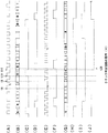
(第4実施形態のクロック判定回路及びPLL判定回路の動作)
図15及び図16を参照して、第4実施形態のクロック判定回路及びPLL判定回路の動作を説明する。図15(A)〜(Q)及び図16(A)〜(Q)は、第4実施形態のクロック判定回路の動作を説明するためのタイミングチャートである。図15(A)〜(Q)は、ピクセルクロックの入力が正常に継続している場合を示し、図16(A)〜(Q)は、ピクセルクロックの入力が正常であるが、PLLにおけるロックが外れた場合を示している。
(Operation of Clock Determination Circuit and PLL Determination Circuit of Fourth Embodiment)
With reference to FIGS. 15 and 16, operations of the clock determination circuit and the PLL determination circuit of the fourth embodiment will be described. FIGS. 15A to 15Q and FIGS. 16A to 16Q are timing charts for explaining the operation of the clock determination circuit of the fourth embodiment. FIGS. 15A to 15Q show the case where the pixel clock input continues normally. FIGS. 16A to 16Q show that the pixel clock input is normal but the lock in the PLL is performed. It shows the case where is off.
図15(A)及び図16(A)は、基準クロックを示している。図15(B)及び図15(B)は、基準クロック計数信号を示している。図15(C)及び図16(C)は、チェック信号を示している。図15(D)及び図16(D)はクリア信号を示している。図15(E)及び図16(E)は、ピクセルクロックを示している。図15(F)及び図16(F)は、ピクセルクロック計数信号を示している。図15(G)及び図16(G)は、コンパレータ信号を示している。図15(H)及び図16(H)は、遅延コンパレータ信号を示している。図15(I)及び図16(I)は、クロック判定信号を示している。図15(J)及び図16(J)は、ピクセルコンパレータ信号を示している。図15(K)及び図16(K)は、遅延ピクセルコンパレータ信号を示している。図15(L)及び図16(L)は、PLLクロックを示している。図15(M)及び図16(M)は、PLLクロック計数信号を示している。図15(N)及び図16(N)は、レジスタ信号を示している。図15(O)及び図16(O)は、PLLコンパレータ信号を示している。図15(P)及び図16(P)は、遅延PLLコンパレータ信号を示している。図15(Q)及び図16(Q)は、PLL判定信号を示している。 FIG. 15A and FIG. 16A show the reference clock. FIG. 15B and FIG. 15B show the reference clock count signal. FIG. 15C and FIG. 16C show check signals. FIG. 15D and FIG. 16D show a clear signal. FIG. 15E and FIG. 16E show pixel clocks. FIG. 15F and FIG. 16F show pixel clock count signals. FIG. 15G and FIG. 16G show the comparator signal. FIG. 15H and FIG. 16H show delayed comparator signals. FIG. 15I and FIG. 16I show clock determination signals. FIG. 15 (J) and FIG. 16 (J) show pixel comparator signals. FIGS. 15K and 16K show delayed pixel comparator signals. FIG. 15L and FIG. 16L show the PLL clock. FIG. 15 (M) and FIG. 16 (M) show the PLL clock count signal. FIG. 15N and FIG. 16N show register signals. FIG. 15 (O) and FIG. 16 (O) show PLL comparator signals. 15 (P) and 16 (P) show the delayed PLL comparator signal. FIG. 15 (Q) and FIG. 16 (Q) show the PLL determination signal.
また、図15(A)〜(Q)及び図16(A)〜(Q)は、横軸に時間軸を取って示し、縦軸には、信号強度を論理レベルで示している。 Further, in FIGS. 15A to 15Q and FIGS. 16A to 16Q, the horizontal axis indicates the time axis, and the vertical axis indicates the signal intensity at a logical level.
同期信号抽出回路20、タイミング信号生成回路22、基準クロックカウンタ222、ピクセルカウンタ232及びフリップフロップ回路240は、リセット端子を有しており、電源投入時にリセットされる。この結果、チェック信号、クリア信号、コンパレータ信号及びクロック判定信号の論理レベルは、電源投入時にいずれもLレベルになるものとする。また、電源投入後は、基準クロック及びピクセルクロックが継続的に入力されるものとする。
The synchronization signal extraction circuit 20, the timing signal generation circuit 22, the reference clock counter 222, the pixel counter 232, and the flip-
先ず、図15を参照して、ピクセルクロックの入力が正常である場合について説明する。 First, the case where the pixel clock input is normal will be described with reference to FIG.
時刻t0において、制御回路16が備える各回路に電源が投入される。電源投入された後、基準クロック及びピクセルクロックが継続的に判定部に入力される。また、PLL26の出力であるPLLクロックも判定部に入力される。このとき、基準クロックカウンタ222は、基準クロックのクロックパルスを計数するので、基準クロック計数信号が示す基準クロック計数値AQは、基準クロックのクロックパルスの立ち上がりエッジごとに、1ずつ増加する。一方、ピクセルクロックカウンタ232及びPLLカウンタ632は計数を行わず、ピクセルクロック計数信号が示すピクセルクロック計数値BQ、及び、PLLクロック計数信号が示すPLLクロック計数値CQは、0のままである。
At time t0, power is turned on to each circuit included in the control circuit 16. After the power is turned on, the reference clock and the pixel clock are continuously input to the determination unit. Further, the PLL clock that is the output of the
時刻t1において、基準クロック計数値AQがチェック値M−1に等しくなると、チェック信号の論理レベルはLレベルからHレベルに変化する。 When the reference clock count value AQ becomes equal to the check value M-1 at time t1, the logic level of the check signal changes from the L level to the H level.
続いて時刻t2において、基準クロック計数値AQがクリア値Mに等しくなると、クリア信号の論理レベルはLレベルからHレベルに変化する。このとき、チェック信号の論理レベルはHレベルからLレベルに変化する。 Subsequently, when the reference clock count value AQ becomes equal to the clear value M at time t2, the logic level of the clear signal changes from the L level to the H level. At this time, the logic level of the check signal changes from H level to L level.
時刻t1においてチェック信号の論理レベルがHレベルになると、フリップフロップ回路240は、次の基準クロックのクロックパルスの立ち上がり時(時刻t2)に、遅延コンパレータ信号をデータ端子Dから取り込む。時刻t2では、遅延コンパレータ信号はLレベルであるので、フリップフロップ回路240の出力信号であるクロック判定信号の論理レベルはLレベルとなる。
When the logic level of the check signal becomes H level at time t1, the flip-
また、時刻t2において、クリア信号の論理レベルがHレベルになると、ピクセルカウンタ232は、数値‘0’を第1ピクセル定数器236からロードする。時刻t3において、クリア信号の論理レベルがHレベルからLレベルになった後、ピクセルカウンタ232は、ピクセルクロックの計数を開始する。
At time t2, when the logic level of the clear signal becomes H level, the pixel counter 232 loads the numerical value “0” from the first pixel
このクリア信号は、PLLカウンタ632のLD端子にも入力されている。時刻t2において、クリア信号の論理レベルがHレベルになると、PLLカウンタ632は、数値‘0’を第1PLL定数器636からロードする。時刻t3において、クリア信号の論理レベルがHレベルからLレベルになった後、ピクセルカウンタ232は、ピクセルクロックの計数を開始し、及び、PLLカウンタ632は、PLLクロックの計数を開始する。
This clear signal is also input to the LD terminal of the PLL counter 632. When the logic level of the clear signal becomes H level at
時刻t4において、ピクセルクロック計数値BQが停止値Nに等しくなると、コンパレータ信号の論理レベルはLレベルからHレベルに変化するとともに、ピクセルクロックの計数が停止する。従って、ピクセルクロック計数値BQは停止値‘N’に等しい状態が続き、その間、コンパレータ信号の論理レベルはHレベルに維持される。 When the pixel clock count value BQ becomes equal to the stop value N at time t4, the logical level of the comparator signal changes from the L level to the H level, and the pixel clock count stops. Accordingly, the pixel clock count value BQ continues to be equal to the stop value 'N', and during that time, the logic level of the comparator signal is maintained at the H level.
なお、ピクセルクロックの計数が停止している間も、基準クロックの計数は独立して行われている。 It should be noted that the reference clock is counted independently while the pixel clock counting is stopped.
時刻t5において、基準クロック計数値AQが、チェック値M−1に等しくなると、チェック信号の論理レベルがHレベルになる。チェック信号の論理レベルがHレベルになると、フリップフロップ回路240は、次の基準クロックのクロックパルスの立ち上がり時(時刻t6)に、遅延コンパレータ信号をデータ端子Dから取り込む。時刻t6では、遅延コンパレータ信号はHレベルであるので、フリップフロップ回路240の出力信号であるクロック判定信号の論理レベルはHレベルとなる。
When the reference clock count value AQ becomes equal to the check value M-1 at time t5, the logical level of the check signal becomes H level. When the logic level of the check signal becomes H level, the flip-
また、時刻t6において、クリア信号の論理レベルがHレベルになると、ピクセルカウンタ232は、数値‘0’を第1ピクセル定数器236からロードする。時刻t7において、クリア信号の論理レベルがHレベルからLレベルになった後、ピクセルクロックカウンタ232は、ピクセルクロックの計数を開始する。
Further, when the logic level of the clear signal becomes H level at time t <b> 6, the pixel counter 232 loads the numerical value “0” from the first pixel
また、時刻t6において、基準クロック計数値AQがクリア値Mに等しくなるので、時刻t7において、基準クロック計数値AQは0にリセットされる。 Further, since the reference clock count value AQ becomes equal to the clear value M at time t6, the reference clock count value AQ is reset to 0 at time t7.
時刻t41でピクセルクロック計数値BQが定数値Lに等しくなると、ピクセルコンパレータ信号が、Hレベルになる。ピクセルコンパレータ遅延器666は、ピクセルコンパレータ信号がHレベルになると、ピクセルコンパレータ信号を遅延させて、PLLクロックのクロックパルスの立ち上がり時(時刻t42)に、遅延ピクセルコンパレータ信号としてレジスタ668に送る。
When the pixel clock count value BQ becomes equal to the constant value L at time t41, the pixel comparator signal becomes H level. When the pixel comparator signal becomes H level, the pixel
遅延ピクセルコンパレータ信号は、レジスタ668のイネーブル端子Eに入力される。遅延ピクセルコンパレータ信号がHレベルになると、レジスタ668は、PLLクロック計数信号を取り込む。取りこまれたPLLクロック計数信号は、PLLクロックの立ち上がり時(t43)に、レジスタ信号として出力され、PLLコンパレータ670に送られる。
The delayed pixel comparator signal is input to the enable terminal E of the register 668. When the delayed pixel comparator signal becomes H level, the register 668 takes in the PLL clock count signal. The captured PLL clock count signal is output as a register signal at the rising edge of the PLL clock (t43) and sent to the
PLLコンパレータ670は、レジスタ信号が示す、レジスタ値と、下限値P及び上限値Qとの比較を行う。例えば、時刻t43で取り込まれたレジスタ値Rが、P≦R≦Qを満たしていないとき、PLLコンパレータ信号はLレベルである。
The
時刻t44でピクセルクロック計数値BQが定数値Lに等しくなると、ピクセルコンパレータ信号は、Hレベルになる。ピクセルコンパレータ遅延器666は、ピクセルコンパレータ信号がHレベルになると、ピクセルコンパレータ信号を遅延させて、PLLクロックのクロックパルスの次の立ち上がり時(時刻t45)に、遅延ピクセルコンパレータ信号としてレジスタ668に送る。
When the pixel clock count value BQ becomes equal to the constant value L at time t44, the pixel comparator signal becomes H level. When the pixel comparator signal becomes H level, the pixel
遅延ピクセルコンパレータ信号は、レジスタ668のイネーブル端子Eに入力される。遅延ピクセルコンパレータ信号がHレベルになると、レジスタ668は、PLLクロック計数信号を取り込む。取りこまれたPLLクロック計数信号は、PLLクロックの立ち上がり時(t46)に、レジスタ信号として出力され、PLLコンパレータ670に送られる。
The delayed pixel comparator signal is input to the enable terminal E of the register 668. When the delayed pixel comparator signal becomes H level, the register 668 takes in the PLL clock count signal. The captured PLL clock count signal is output as a register signal at the rising edge of the PLL clock (t46) and sent to the
PLLコンパレータ670は、レジスタ668に取り込まれているPLLクロック計数値CQを示すレジスタ値と、下限値P及び上限値Qとの比較を行う。例えば、時刻t46で取り込まれたレジスタ値Sが、P≦S≦Qを満たしているとき、PLLコンパレータ信号はHレベルになる。
The
このPLLコンパレータ信号は、PLLコンパレータ遅延器644で遅延され、遅延PLLコンパレータ信号として、フリップフロップ回路640に送られる。
This PLL comparator signal is delayed by a
時刻t47において、基準クロック計数値AQが、チェック値M−1に等しくなると、チェック信号の論理レベルがHレベルになる。チェック信号の論理レベルがHレベルになると、フリップフロップ回路640は、次の基準クロックのクロックパルスの立ち上がり時(時刻t48)に、遅延PLLコンパレータ信号をデータ端子Dから取り込む。時刻t48では、遅延PLLコンパレータ信号はHレベルであるので、フリップフロップ回路640の出力信号であるPLL判定信号の論理レベルはHレベルとなる。
At time t47, when the reference clock count value AQ becomes equal to the check value M-1, the logical level of the check signal becomes H level. When the logic level of the check signal becomes H level, the flip-
次に、図16を参照して、ピクセルクロックの入力が正常であるが、PLLにおけるロックが外れた場合について説明する。 Next, a case where the pixel clock input is normal but the PLL is unlocked will be described with reference to FIG.
時刻t50でロックが外れたものとする。 Assume that the lock is released at time t50.
時刻t51でピクセルクロック計数値BQが定数値Lに等しくなると、ピクセルコンパレータ信号は、Hレベルになる。ピクセルコンパレータ遅延器666は、ピクセルコンパレータ信号がHレベルになると、ピクセルコンパレータ信号を遅延させて、PLLクロックのクロックパルスの次の立ち上がり時(時刻t52)に、遅延ピクセルコンパレータ信号としてレジスタ668に送る。
When the pixel clock count value BQ becomes equal to the constant value L at time t51, the pixel comparator signal becomes H level. When the pixel comparator signal becomes H level, the pixel
遅延ピクセルコンパレータ信号は、レジスタ668のイネーブル端子Eに入力される。遅延ピクセルコンパレータ信号がHレベルになると、レジスタ668は、PLLクロックの立ち上がり時(t53)に、PLLクロック計数信号を取り込む。取りこまれたPLLクロック計数信号は、レジスタ信号として出力され、PLLコンパレータ670に送られる。
The delayed pixel comparator signal is input to the enable terminal E of the register 668. When the delayed pixel comparator signal becomes H level, the register 668 captures the PLL clock count signal at the rising edge of the PLL clock (t53). The captured PLL clock count signal is output as a register signal and sent to the
PLLコンパレータ670は、レジスタ値と、下限値P及び上限値Qとの比較を行う。ここで、時刻t50でPLLのロックが外れた場合、時刻t53で取り込まれたレジスタ値Vは、P≦V≦Qを満たさない。従って、PLLコンパレータ信号はLレベルになる。
The
時刻t55において、基準クロック計数値AQが、チェック値M−1に等しくなると、チェック信号の論理レベルがHレベルになる。チェック信号の論理レベルがHレベルになると、フリップフロップ回路640は、次の基準クロックのクロックパルスの立ち上がり時(時刻t56)に、遅延PLLコンパレータ信号をデータ端子Dから取り込む。時刻t56では、遅延PLLコンパレータ信号はLレベルであるので、フリップフロップ回路640の出力信号であるPLL判定信号の論理レベルはLレベルとなる。
When the reference clock count value AQ becomes equal to the check value M-1 at time t55, the logic level of the check signal becomes H level. When the logic level of the check signal becomes H level, the flip-
t50でロックが外れた後、再びロックイン過程が行われ、ロックされると、図15を参照して説明したのと同様の過程を経て、時刻t57で、PLL判定信号はHレベルになる。 After the lock is released at t50, the lock-in process is performed again. When the lock-in process is performed, the PLL determination signal becomes H level at time t57 through the same process as described with reference to FIG.
第4実施形態の制御回路では、同期信号抽出回路が、ピクセルクロックで動作し、タイミング信号生成回路は、PLLクロックで動作する。このように構成することで、入力される画像信号のクロック周波数と異なる周波数で画像処理装置を駆動させることが可能になる。 In the control circuit of the fourth embodiment, the synchronization signal extraction circuit operates with a pixel clock, and the timing signal generation circuit operates with a PLL clock. With this configuration, the image processing apparatus can be driven at a frequency different from the clock frequency of the input image signal.
また、PLL判定回路で生成されるPLL判定信号は、PLLにおいてロックされているときは、正常を示す信号を出力し、PLLにおいてロックが外れているときは、異常を示す信号を出力する。このため、PLLでのロックイン状態に応じてタイミング信号を生成することができる。 The PLL determination signal generated by the PLL determination circuit outputs a signal indicating normality when the PLL is locked, and outputs a signal indicating abnormality when the PLL is unlocked. For this reason, a timing signal can be generated according to the lock-in state in the PLL.
なお、第4実施形態の制御回路について、フェイルセーフ回路が、さらに第3実施形態の制御回路と同様に第1同期判定回路と第2同期判定回路を備える構成にしても良い。 In addition, about the control circuit of 4th Embodiment, you may make it a structure in which a fail safe circuit is further provided with the 1st synchronization determination circuit and the 2nd synchronization determination circuit similarly to the control circuit of 3rd Embodiment.
このように構成すれば、ピクセルクロックだけではなく、同期信号の入力状態も判定するので、画像信号や同期信号に異常が発生した場合にも、タイミング信号の出力を停止することができる。また、タイミング信号生成回路に入力される信号を判定に用いることで、特許文献1に記載の構成よりも時系列的に早い段階で異常検出が可能になる。この結果、異常発生時の制御が、より容易になる。
With this configuration, since not only the pixel clock but also the input state of the synchronization signal is determined, the output of the timing signal can be stopped even when an abnormality occurs in the image signal or the synchronization signal. Further, by using a signal input to the timing signal generation circuit for determination, it is possible to detect an abnormality at an earlier stage in time series than the configuration described in
以上説明した第4実施形態の制御回路では、PLLクロックとピクセルクロックの周波数が等しい例について説明したが、PLL26において、PLLクロックの周波数をピクセルクロックの周波数と異なるように構成することもできる。この場合、下限値P、上限値Q、PLL比較基準値Lを適宜設定すれば良い。
In the control circuit of the fourth embodiment described above, an example in which the PLL clock and the pixel clock have the same frequency has been described. However, the
(第4実施形態の制御回路の変形例)
図17及び図18を参照して、第4実施形態の制御回路の変形例について説明する。図17は、制御回路の変形例の概略構成図である。図18は、PLLの概略構成図である。
(Modification of Control Circuit of Fourth Embodiment)
A modification of the control circuit of the fourth embodiment will be described with reference to FIGS. 17 and 18. FIG. 17 is a schematic configuration diagram of a modified example of the control circuit. FIG. 18 is a schematic configuration diagram of a PLL.
この変形例の制御回路17は、初期化信号生成回路604を備えている点が、図13を参照して説明した第4実施形態の構成と異なっている。 The control circuit 17 of this modification is different from the configuration of the fourth embodiment described with reference to FIG. 13 in that it includes an initialization signal generation circuit 604.
初期化信号生成回路604は、任意好適な従来周知の論理微分回路で構成することができる。初期化信号生成回路604には、判定部46で生成された判定信号が入力され、初期化信号生成回路604からは、初期化信号が出力される。判定信号がHレベルからLレベルに変化するときに、初期化信号は、所定の時間、Hレベルとなり、それ以外のときは、定常的にLレベルである。 The initialization signal generation circuit 604 can be configured by any suitable conventionally known logical differentiation circuit. The initialization signal generation circuit 604 receives the determination signal generated by the determination unit 46, and the initialization signal generation circuit 604 outputs an initialization signal. When the determination signal changes from the H level to the L level, the initialization signal becomes the H level for a predetermined time, and at other times, the initialization signal is constantly at the L level.
PLL28は、第1分周器702、第2分周器704、位相比較器(PC)706、ローパスフィルタ(LPF)708及び電圧制御発振器(VCO)710を備えている。
The
ピクセルクロックは第1分周器702に入力される。第1分周器702の出力と、第2分周器704の出力とが、位相比較器706に入力される。第1分周器702の出力と、第2分周器704の出力の位相差に対応する電圧信号は、位相差信号として位相比較器706から出力される。この位相差信号がローパスフィルタ708を通過した後、電圧制御発振器710に送られる。電圧制御発振器710は、位相差信号の電圧に応じて定まる周波数の信号を出力する。この電圧制御発振器710の出力信号は2分岐され、一方は第2分周器704に送られ、他方はPLLクロックとして、PLL28から出力される。
The pixel clock is input to the first frequency divider 702. The output of the first frequency divider 702 and the output of the second frequency divider 704 are input to the
このPLL28を動作させることにより、第1分周器702と第2分周器704の出力が同期する。すなわち、PLL28に入力されるピクセルクロックと、PLL28から出力されるPLLクロックとが同期する。なお、PLL28から出力されるPLLクロックの周波数は、電圧制御発振器710の基準周波数と、第1分周器702及び第2分周器704における分周の大きさによって定めることができる。
By operating the
ここでは、位相比較器706とローパスフィルタ708の間に第1スイッチ712が設けられている。また、電圧供給端子716と電圧制御発振器710の入力端子との間に第2スイッチ714が設けられている。
Here, a
第1スイッチ712及び第2スイッチ714は、初期化信号のレベルによって、ON/OFFされる。第1スイッチ712は、初期化信号がLレベルのとき、ON状態となり、HレベルのときOFF状態となる。一方、第2スイッチ714は、初期化信号がHレベルのとき、ON状態となり、LレベルのときOFF状態となる。
The
電圧供給端子716は、電圧制御発振器710の特性に応じて定まる所定の電位となっている。例えば、電圧制御発振器710の入力電圧が低くなると、出力信号の周波数が低くなる場合は、電圧供給端子716の電位を接地電位GNDとする。一方、電圧制御発振器の入力電圧が高くなると、出力信号の周波数が低くなる場合は、電圧供給端子716の電位を高電位、例えば、電源電圧の電位VDDとする。
The
図19は、この構成例のPLLの動作を示すタイミングチャートである。 FIG. 19 is a timing chart showing the operation of the PLL of this configuration example.
図19(A)は、クロック判定信号を示している。図19(B)は、PLL判定信号を示している。図19(C)は、判定信号を示している。図19(D)は、初期化信号を示している。図19(E)は、電圧制御発振器(VCO)における周波数を示している。 FIG. 19A shows a clock determination signal. FIG. 19B shows a PLL determination signal. FIG. 19C shows a determination signal. FIG. 19D shows an initialization signal. FIG. 19E shows the frequency in the voltage controlled oscillator (VCO).
時刻t0において制御回路17に電源投入すると、各信号はLレベルになる。また、このとき、電圧制御発振器710の出力周波数は動作範囲中、最も低い状態になる。
When the control circuit 17 is powered on at time t0, each signal becomes L level. At this time, the output frequency of the voltage controlled
その後、t80においてクロック判定信号がHレベルになる。この段階では、PLL28はロックイン過程中であり、PLL判定信号はLレベルである。従って、時刻t80では、クロック判定信号とPLL判定信号の論理積である判定信号はLレベルである。
Thereafter, the clock determination signal becomes H level at t80. At this stage, the
その後、時刻t81においてロックインが完了し安定状態になると、PLL判定信号はHレベルになる。このとき、判定信号はHレベルになる。 Thereafter, when the lock-in is completed and becomes stable at time t81, the PLL determination signal becomes H level. At this time, the determination signal becomes H level.
次に、時刻t82において、PLL28におけるロックが外れたとする。PLL28のロックが外れると、PLL判定信号及び判定信号がLレベルになる。
Next, it is assumed that the
判定信号がHレベルからLレベルに変化すると、初期化信号が所定の期間Hレベルになる。初期化信号がHレベルになると、PLLの初期化が行われ、再び、PLLのロックイン過程が行われる。その後、時刻t83で安定する。 When the determination signal changes from H level to L level, the initialization signal becomes H level for a predetermined period. When the initialization signal becomes H level, the PLL is initialized and the PLL lock-in process is performed again. Then, it stabilizes at time t83.
次に、時刻t84において、クロック判定信号がLレベルになったとする。この場合、PLL判定信号がHレベルのままであっても、判定信号がLレベルになるので、PLLの初期化が行われる。 Next, it is assumed that the clock determination signal becomes L level at time t84. In this case, even if the PLL determination signal remains at the H level, the determination signal becomes the L level, so that the PLL is initialized.
PLL28のロックが外れると、PLL28は、目標と異なる周波数で発振を始めるが、この発振周波数が、目標よりも高くなると、各内部回路の動作が異常をきたす恐れがある。この結果、電圧制御発振器の周波数が、目標値よりも高い場合であっても、位相比較器706が判定を誤って、より電圧制御発振器の周波数を高める方向にその出力を行うことが起こりうる。このような事象が起こると、一度電源をOFFにしない限り、PLLは正常に動作しない。
When the
これに対し、この実施形態の構成によれば、判定信号がLレベルになる都度、PLLの初期化を行う。また、この初期化においては、電圧制御発振器の周波数が必ず低い周波数から動作を再開するので、PLLの内部回路が、想定以上に高い周波数の入力による誤動作が起こることを防ぐことができる。 On the other hand, according to the configuration of this embodiment, the PLL is initialized every time the determination signal becomes L level. In this initialization, since the operation of the voltage controlled oscillator is always restarted from a low frequency, it is possible to prevent the PLL internal circuit from malfunctioning due to an input of a frequency higher than expected.
10、11、12、13、14、15、16、17 制御回路
20 同期信号抽出回路
22 タイミング信号生成回路
24 基準クロック発生手段
26、28 PLL
30、31、32、33、34、35、36、37 フェイルセーフ回路
40、41、42、43、44、45、46 判定部
90、91、92 保護ゲート部
94 ANDゲート
96 ORゲート
97 第1保護ゲート回路
98 第2保護ゲート回路
200、201、202 クロック判定回路
220 基準クロック計数部
222 基準クロックカウンタ
224、406 デコーダ
230 ピクセルクロック計数部
232 ピクセルカウンタ
234 ピクセルコンパレータ
236 第1ピクセル定数器
238 第2ピクセル定数器
240、640 フリップフロップ回路
242 クリア信号遅延器
244 コンパレータ信号遅延器
300、310、320 出力ゲート部
302、304、314、318、322、324 増幅回路
312 OR回路
316 テスト端子
326 反転回路
400 動作判定回路
402、408、430、602 ANDゲート
404 カウンタ
410 第1同期判定回路
420 第2同期判定回路
440 分周器
600 PLL判定回路
604 初期化信号生成回路
630 PLLクロック計数部
632 PLLカウンタ
634、670 PLLコンパレータ
636 第1PLL定数器
638 第2PLL定数器
644 PLLコンパレータ遅延器
660 PLL判定部
662 コンパレータ
664 PLL比較基準定数器
666 コンパレータ遅延器
668 レジスタ
672 下限定数器
674 上限定数器
702 第1分周器
704 第2分周期
706 位相比較器(PC)
708 ローパスフィルタ(LPF)
710 電圧制御発振器(VCO)
712 第1スイッチ
714 第2スイッチ
716 電圧供給端子
10, 11, 12, 13, 14, 15, 16, 17 Control circuit 20 Synchronization signal extraction circuit 22 Timing signal generation circuit 24 Reference clock generation means 26, 28 PLL
30, 31, 32, 33, 34, 35, 36, 37 Fail safe circuit 40, 41, 42, 43, 44, 45, 46
708 Low pass filter (LPF)
710 Voltage controlled oscillator (VCO)
712
Claims (21)
前記クロック判定信号が正常を示すとき、タイミング信号を通過させる保護ゲート部と
を備えることを特徴とするフェイルセーフ回路。 A clock determination circuit that determines whether or not the input of the pixel clock is normal using a count value of a pixel clock within a period determined by a count value of a reference clock, and generates a clock determination signal indicating the result of the determination A determination unit that outputs the clock determination signal as a determination signal;
A fail-safe circuit comprising: a protection gate section that allows a timing signal to pass when the clock determination signal indicates normality.
前記ピクセルクロックの計数値が定める期間内であって、タイミング信号が2分岐された一方に含まれるスタートパルスが持続している期間内は、前記タイミング信号が正常であることを示す動作判定信号を生成する動作判定回路
を有し、前記クロック判定信号と前記動作判定信号の論理積を判定信号として出力する判定部と、
前記クロック判定信号及び前記動作判定信号が正常を示すとき、前記タイミング信号が2分岐された他方を通過させる保護ゲート部と
を備えることを特徴とするフェイルセーフ回路。 A clock determination circuit that determines whether or not the input of the pixel clock is normal using a count value of a pixel clock within a period determined by a count value of a reference clock, and generates a clock determination signal indicating the result of the determination And an operation determination indicating that the timing signal is normal within a period determined by a count value of the pixel clock and within a period in which a start pulse included in one of the two branched timing signals is continued. A determination unit that includes an operation determination circuit that generates a signal, and outputs a logical product of the clock determination signal and the operation determination signal as a determination signal;
A fail-safe circuit comprising: a protection gate section that allows the timing signal to pass through the other branched into two when the clock determination signal and the operation determination signal indicate normality.
前記基準クロックを計数して、計数結果である基準クロック計数値が予め設定されているクリア値Mに等しいときにクリア信号を第1レベルから第2レベルに変化させて出力するとともに、前記基準クロック計数値を0にリセットし、前記基準クロック計数値が予め設定されているチェック値M−1に等しいときにチェック信号を第1レベルから第2レベルに変化させて出力する基準クロック計数部と、
前記ピクセルクロックを計数して、計数結果であるピクセルクロック計数値が予め設定されている停止値Nに等しくなると、コンパレータ信号を第1レベルから第2レベルに変化させて出力するとともに、計数動作を停止し、前記クリア信号が第2レベルのときに前記ピクセルクロック計数値を0にリセットするピクセルクロック計数部と、
前記チェック信号が第2レベルのときに、前記コンパレータ信号を取り込み、前記クロック判定信号として出力するフリップフロップ回路と
を備えることを特徴とする請求項1又は2に記載のフェイルセーフ回路。 The clock determination circuit includes:
The reference clock is counted, and when a reference clock count value as a counting result is equal to a preset clear value M, a clear signal is changed from the first level to the second level and output, and the reference clock is output. A reference clock counter for resetting the count value to 0 and changing the check signal from the first level to the second level when the reference clock count value is equal to a preset check value M−1;
The pixel clock is counted, and when the pixel clock count value as a count result is equal to a preset stop value N, the comparator signal is changed from the first level to the second level and output, and the counting operation is performed. A pixel clock counter that stops and resets the pixel clock count value to 0 when the clear signal is at a second level;
3. The fail-safe circuit according to claim 1, further comprising: a flip-flop circuit that takes in the comparator signal and outputs it as the clock determination signal when the check signal is at a second level.
前記コンパレータ信号を遅延させて前記フリップフロップ回路に送るピクセル判定信号遅延器と
を備えることを特徴とする請求項3に記載のフェイルセーフ回路。 A clear signal delay device that delays the clear signal and sends it to the pixel clock counter;
The fail-safe circuit according to claim 3, further comprising a pixel determination signal delay device that delays the comparator signal and sends the delayed signal to the flip-flop circuit.
第2同期信号の計数値が定める期間内の第1同期信号の計数値を用いて、前記第1同期信号が正常であるか否かを判定し、当該判定の結果を示す第1同期判定信号を生成する第1同期判定回路、及び
前記基準クロックの計数値が定める期間内の前記第2同期信号の計数値を用いて、前記第2同期信号が正常であるか否かを判定し、当該判定の結果を示す第2同期判定信号を生成する第2同期判定回路
を有し、前記クロック判定信号、前記第1同期判定信号及び前記第2同期判定信号の論理積を判定信号として出力する判定部と、
前記クロック判定信号、前記第1同期判定信号及び前記第2同期判定信号が正常を示すとき、タイミング信号を通過させる保護ゲート部と
を備えることを特徴とするフェイルセーフ回路。 A clock determination circuit that determines whether or not the input of the pixel clock is normal using a count value of a pixel clock within a period determined by a count value of a reference clock, and generates a clock determination signal indicating the result of the determination ,
A first synchronization determination signal indicating whether or not the first synchronization signal is normal using a count value of the first synchronization signal within a period determined by a count value of the second synchronization signal and indicating a result of the determination A first synchronization determination circuit for generating the first synchronization signal, and using the count value of the second synchronization signal within a period determined by the count value of the reference clock to determine whether the second synchronization signal is normal, A second synchronization determination circuit that generates a second synchronization determination signal indicating a determination result, and that outputs a logical product of the clock determination signal, the first synchronization determination signal, and the second synchronization determination signal as a determination signal And
A fail-safe circuit comprising: a protection gate section that allows a timing signal to pass when the clock determination signal, the first synchronization determination signal, and the second synchronization determination signal indicate normality.
第1クロックを計数して、計数結果である第1クロック計数値が予め設定されているクリア値Mに等しいときにクリア信号を第1レベルから第2レベルに変化させて出力するとともに、前記第1クロック計数値を0にリセットし、前記第1クロック計数値が予め設定されているチェック値M−1に等しいときにチェック信号を第1レベルから第2レベルに変化させて出力する第1クロック計数部と、
第2クロックを計数して、計数結果である第2クロック計数値が予め設定されている停止値Nに等しいときに、コンパレータ信号を第1レベルから第2レベルに変化させて出力するとともに、計数動作を停止し、前記クリア信号が第2レベルのときに前記第2クロック計数値を0にリセットする第2クロック計数部と、
前記チェック信号が第2レベルのときに、前記コンパレータ信号を取り込み、前記同期判定信号として出力するフリップフロップ回路と
を備え、
前記クロック判定回路には、第1クロック及び第2クロックとして前記基準クロック及び前記ピクセルクロックがそれぞれ入力され、
前記クロック判定回路からは、同期判定信号として、前記クロック判定信号が出力され、
前記第1同期判定回路には、第1クロック及び第2クロックとして前記第2同期信号及び前記第1同期信号がそれぞれ入力され、
前記第1同期判定回路からは、同期判定信号として、前記第1同期判定信号が出力され、
前記第2同期判定回路には、第1クロック及び第2クロックとして前記基準クロック及び前記第2同期信号がそれぞれ入力され、
前記第2同期判定回路からは、同期判定信号として、前記第2同期判定信号が出力される
ことを特徴とする請求項5に記載のフェイルセーフ回路。 The clock determination circuit, the first synchronization determination circuit, and the second synchronization determination circuit each count the first clock, and when the first clock count value that is a count result is equal to a preset clear value M The clear signal is changed from the first level to the second level and output, the first clock count value is reset to 0, and the first clock count value is equal to the preset check value M-1. A first clock counting unit that sometimes changes the check signal from the first level to the second level and outputs it;
The second clock is counted, and when the second clock count value as a count result is equal to a preset stop value N, the comparator signal is changed from the first level to the second level and output, and the count is performed. A second clock counter that stops operation and resets the second clock count value to 0 when the clear signal is at a second level;
A flip-flop circuit that takes in the comparator signal and outputs it as the synchronization determination signal when the check signal is at the second level;
The clock determination circuit receives the reference clock and the pixel clock as a first clock and a second clock, respectively.
From the clock determination circuit, the clock determination signal is output as a synchronization determination signal,
The first synchronization determination circuit receives the second synchronization signal and the first synchronization signal as a first clock and a second clock, respectively.
The first synchronization determination circuit outputs the first synchronization determination signal as a synchronization determination signal.
The second synchronization determination circuit receives the reference clock and the second synchronization signal as a first clock and a second clock, respectively.
6. The failsafe circuit according to claim 5, wherein the second synchronization determination circuit outputs the second synchronization determination signal as a synchronization determination signal.
前記第1クロック計数部から出力されたクリア信号を遅延させて前記第2クロック計数部に送るクリア信号遅延器と、
前記第2クロック計数部から出力されたコンパレータ信号を遅延させて前記フリップフロップ回路に送るコンパレータ信号遅延器と
を備えることを特徴とする請求項6に記載のフェイルセーフ回路。 The clock determination circuit, the first synchronization determination circuit, and the second synchronization determination circuit are:
A clear signal delay unit that delays the clear signal output from the first clock counting unit and sends the delayed signal to the second clock counting unit;
The fail-safe circuit according to claim 6, further comprising a comparator signal delay device that delays the comparator signal output from the second clock counting unit and sends the delayed signal to the flip-flop circuit.
前記基準クロックの計数値が定める期間内の、前記ピクセルクロックとPLLクロックの計数値を比較して前記PLLクロックが正常であるか否かを判定し、当該判定の結果を示すPLL判定信号を生成するPLL判定回路と、
を有し、前記クロック判定信号と前記PLL判定信号の論理積を判定信号として出力する判定部と、
前記クロック判定信号と前記PLL判定信号が正常を示すとき、タイミング信号を通過させる保護ゲート部と
を備えることを特徴とするフェイルセーフ回路。 A clock determination circuit that determines whether or not the pixel clock is normal using a count value of a pixel clock within a period determined by a count value of a reference clock, and generates a clock determination signal indicating a result of the determination;
Compares the count values of the pixel clock and PLL clock within a period determined by the reference clock count value to determine whether or not the PLL clock is normal, and generates a PLL determination signal indicating the result of the determination A PLL decision circuit to perform,
A determination unit that outputs a logical product of the clock determination signal and the PLL determination signal as a determination signal;
A fail-safe circuit comprising: a protection gate section that allows a timing signal to pass when the clock determination signal and the PLL determination signal indicate normality.
前記基準クロックを計数して、計数結果である基準クロック計数値が予め設定されているクリア値Mに等しいときにクリア信号を第1レベルから第2レベルに変化させて出力するとともに、前記基準クロック計数値を0にリセットし、前記基準クロック計数値が予め設定されているチェック値M−1に等しいときにチェック信号を第1レベルから第2レベルに変化させて出力する基準クロック計数部と、
前記ピクセルクロックを計数して、計数結果であるピクセルクロック計数値が予め設定されている停止値Nに等しいときに、ピクセルクロック計数信号を第1レベルから第2レベルに変化させて出力するとともに、計数動作を停止し、前記クリア信号が第2レベルのときに前記ピクセルクロック計数値を0にリセットするピクセルクロック計数部と、
前記チェック信号が第2レベルのときに、前記ピクセルクロック計数信号を取り込み、クロック判定信号として出力するフリップフロップ回路と
を備え、
前記PLL判定回路は、
前記PLLクロックを計数して、計数結果であるPLLクロック計数値を示すPLLクロック計数信号を出力するPLLカウンタと、
前記ピクセルクロック計数値が予め設定されているピクセル比較基準値Lに等しくなると、前記PLLクロック計数信号を取り込むレジスタと、
前記レジスタが取り込んだ前記PLLクロック計数信号が示すPLLクロック計数値を、予め設定されている下限値P及び上限値Qと比較し、前記PLLクロック計数値が前記下限値P以上かつ前記上限値Q以下であるときPLL判定信号を第1レベルから第2レベルに変化させて出力するPLLコンパレータと
を備えることを特徴とする請求項8に記載のフェイルセーフ回路。 The clock determination circuit includes:
The reference clock is counted, and when a reference clock count value as a counting result is equal to a preset clear value M, a clear signal is changed from the first level to the second level and output, and the reference clock is output. A reference clock counter for resetting the count value to 0 and changing the check signal from the first level to the second level when the reference clock count value is equal to a preset check value M−1;
The pixel clock is counted, and when the pixel clock count value as a count result is equal to a preset stop value N, the pixel clock count signal is changed from the first level to the second level and is output, A pixel clock counter that stops the counting operation and resets the pixel clock count value to 0 when the clear signal is at the second level;
A flip-flop circuit that captures the pixel clock count signal and outputs it as a clock determination signal when the check signal is at the second level;
The PLL determination circuit includes:
A PLL counter that counts the PLL clock and outputs a PLL clock count signal indicating a PLL clock count value as a counting result;
A register that captures the PLL clock count signal when the pixel clock count value is equal to a preset pixel comparison reference value L;
The PLL clock count value indicated by the PLL clock count signal fetched by the register is compared with a preset lower limit value P and upper limit value Q, and the PLL clock count value is greater than or equal to the lower limit value P and the upper limit value Q. 9. The fail-safe circuit according to claim 8, further comprising: a PLL comparator that outputs a PLL determination signal by changing the PLL determination signal from the first level to the second level when:
前記基準クロックの計数値が定める期間内の、前記ピクセルクロックとPLLクロックの計数値を比較して前記PLLクロックが正常であるか否かを判定し、当該判定の結果を示すPLL判定信号を生成するPLL判定回路、
第2同期信号の計数値が定める期間内の第1同期信号の計数値を用いて、前記第1同期信号が正常であるか否かを判定し、当該判定の結果を示す第1同期判定信号を生成する第1同期判定回路、及び
前記基準クロックの計数値が定める期間内の第2同期信号の計数値を用いて、前記第2同期信号が正常であるか否かを判定し、当該判定の結果を示す第2同期判定信号を生成する第2同期判定回路
を有し、前記クロック判定信号、前記PLL判定信号、前記第1同期判定信号及び前記第2同期判定信号の論理積を判定信号として出力する判定部と、
前記クロック判定信号、前記PLL判定信号、前記第1同期判定信号及び前記第2同期判定信号が正常を示すとき、タイミング信号を通過させる保護ゲート部と
を備えることを特徴とするフェイルセーフ回路。 A clock determination circuit that determines whether or not the pixel clock is normal using a count value of a pixel clock within a period determined by a count value of a reference clock, and generates a clock determination signal indicating a result of the determination;
Compares the count values of the pixel clock and PLL clock within a period determined by the reference clock count value to determine whether or not the PLL clock is normal, and generates a PLL determination signal indicating the result of the determination A PLL determination circuit to perform,
A first synchronization determination signal indicating whether or not the first synchronization signal is normal using a count value of the first synchronization signal within a period determined by a count value of the second synchronization signal and indicating a result of the determination A first synchronization determination circuit for generating the second synchronization signal using a count value of the second synchronization signal within a period determined by the count value of the reference clock, and the determination A second synchronization determination circuit that generates a second synchronization determination signal indicating the result of the determination, and a logical product of the clock determination signal, the PLL determination signal, the first synchronization determination signal, and the second synchronization determination signal is a determination signal A determination unit that outputs as
A fail-safe circuit comprising: a protection gate section that allows a timing signal to pass when the clock determination signal, the PLL determination signal, the first synchronization determination signal, and the second synchronization determination signal indicate normality.
第1クロックを計数して、計数結果である第1クロック計数値が予め設定されているクリア値Mに等しいときにクリア信号を第1レベルから第2レベルに変化させて出力するとともに、前記第1クロック計数値を0にリセットし、前記第1クロック計数値が予め設定されているチェック値M−1に等しいときにチェック信号を第1レベルから第2レベルに変化させて出力する第1クロック計数部と、
第2クロックを計数して、計数結果である第2クロック計数値が予め設定されている停止値Nに等しいときに、コンパレータ信号を第1レベルから第2レベルに変化させて出力するとともに、計数動作を停止し、前記クリア信号が第2レベルのときに前記第2クロック計数値を0にリセットする第2クロック計数部と、
前記チェック信号が第2レベルのときに、前記コンパレータ信号を取り込み、前記同期判定信号として出力するフリップフロップ回路と
を備え、
前記クロック判定回路には、第1クロック及び第2クロックとして前記基準クロック及び前記ピクセルクロックがそれぞれ入力され、
前記クロック判定回路からは、同期判定信号として、前記クロック判定信号が出力され、
前記第1同期判定回路には、第1クロック及び第2クロックとして前記第2同期信号及び前記第1同期信号がそれぞれ入力され、
前記第1同期判定回路からは、同期判定信号として、前記第1同期判定信号が出力され、
前記第2同期判定回路には、第1クロック及び第2クロックとして前記基準クロック及び前記第2同期信号がそれぞれ入力され、
前記第2同期判定回路からは、同期判定信号として、前記第2同期判定信号が出力され、
前記PLL判定回路は、
PLLクロックを計数して、計数結果であるPLLクロック計数値を示すPLLクロック計数信号を出力するPLLカウンタと、
前記ピクセルクロック計数値が予め設定されているピクセル比較基準値Lに等しくなると、前記PLLクロック計数信号を取り込むレジスタと、
前記レジスタが取り込んだ前記PLLクロック計数信号が示す前記PLLクロック計数値を、予め設定されている下限値P及び上限値Qと比較し、前記PLLクロック計数値が下限値P以上かつ上限値Q以下であるときPLL判定信号を第1レベルから第2レベルに変化させて出力するPLLコンパレータとを備える
ことを特徴とする請求項10に記載のフェイルセーフ回路。 The clock determination circuit, the first synchronization determination circuit, and the second synchronization determination circuit each count the first clock, and when the first clock count value that is a count result is equal to a preset clear value M The clear signal is changed from the first level to the second level and output, the first clock count value is reset to 0, and the first clock count value is equal to the preset check value M-1. A first clock counting unit that sometimes changes the check signal from the first level to the second level and outputs it;
The second clock is counted, and when the second clock count value as a count result is equal to a preset stop value N, the comparator signal is changed from the first level to the second level and output, and the count is performed. A second clock counter that stops operation and resets the second clock count value to 0 when the clear signal is at a second level;
A flip-flop circuit that takes in the comparator signal and outputs it as the synchronization determination signal when the check signal is at the second level;
The clock determination circuit receives the reference clock and the pixel clock as a first clock and a second clock, respectively.
From the clock determination circuit, the clock determination signal is output as a synchronization determination signal,
The first synchronization determination circuit receives the second synchronization signal and the first synchronization signal as a first clock and a second clock, respectively.
The first synchronization determination circuit outputs the first synchronization determination signal as a synchronization determination signal.
The second synchronization determination circuit receives the reference clock and the second synchronization signal as a first clock and a second clock, respectively.
From the second synchronization determination circuit, the second synchronization determination signal is output as a synchronization determination signal,
The PLL determination circuit includes:
A PLL counter that counts the PLL clock and outputs a PLL clock count signal indicating a PLL clock count value that is a count result;
A register that captures the PLL clock count signal when the pixel clock count value is equal to a preset pixel comparison reference value L;
The PLL clock count value indicated by the PLL clock count signal taken in by the register is compared with a preset lower limit value P and upper limit value Q, and the PLL clock count value is not less than the lower limit value P and not more than the upper limit value Q. 11. A fail-safe circuit according to claim 10, further comprising a PLL comparator that outputs the PLL determination signal by changing the PLL determination signal from the first level to the second level.
前記同期信号からタイミング信号を生成するタイミング信号生成回路と、
請求項1〜4のいずれか一項に記載のフェイルセーフ回路と
を備えることを特徴とする制御回路。 A synchronization signal extraction circuit for extracting the synchronization signal from the image signal;
A timing signal generation circuit that generates a timing signal from the synchronization signal;
A control circuit comprising the fail-safe circuit according to claim 1.
前記第1同期信号及び第2同期信号からタイミング信号を生成するタイミング信号生成回路と、
請求項5〜7のいずれか一項に記載のフェイルセーフ回路と
を備えることを特徴とする制御回路。 A synchronization signal extraction circuit for extracting the first synchronization signal and the second synchronization signal from the image signal;
A timing signal generation circuit for generating a timing signal from the first synchronization signal and the second synchronization signal;
A control circuit comprising the fail-safe circuit according to claim 5.
前記同期信号からタイミング信号を生成するタイミング信号生成回路と、
ピクセルクロックと同期するPLLクロックを生成するPLL回路と、
請求項8又は9に記載のフェイルセーフ回路と
を備えることを特徴とする制御回路。 A synchronization signal extraction circuit for extracting the synchronization signal from the image signal;
A timing signal generation circuit that generates a timing signal from the synchronization signal;
A PLL circuit for generating a PLL clock synchronized with the pixel clock;
A control circuit comprising the fail-safe circuit according to claim 8.
前記第1同期信号及び第2同期信号からタイミング信号を生成するタイミング信号生成回路と、
ピクセルクロックと同期するPLLクロックを生成するPLL回路と、
請求項10又は11に記載のフェイルセーフ回路と
を備えることを特徴とする制御回路。 A synchronization signal extraction circuit for extracting the first synchronization signal and the second synchronization signal from the image signal;
A timing signal generation circuit for generating a timing signal from the first synchronization signal and the second synchronization signal;
A PLL circuit for generating a PLL clock synchronized with the pixel clock;
A control circuit comprising the fail-safe circuit according to claim 10.
前記PLL回路は、前記初期化信号の入力に応答して、初期化される
ことを特徴とする請求項14又は15に記載の制御回路。 The fail safe circuit includes an initialization signal generation circuit that generates an initialization signal when the determination signal changes from a normal state to an abnormal state;
16. The control circuit according to claim 14, wherein the PLL circuit is initialized in response to an input of the initialization signal.
ことを特徴とする請求項16に記載の制御回路。 17. The control circuit according to claim 16, wherein the voltage controlled oscillator provided in the PLL circuit has an oscillation frequency that falls within an operating range in response to the input of the initialization signal.
ことを特徴とする請求項12〜17のいずれか一項に記載の制御回路。 The control circuit according to any one of claims 12 to 17, wherein the timing signal generation circuit is reset when the determination signal indicates an abnormality.
ことを特徴とする請求項12〜18のいずれか一項に記載の制御回路。 The control according to claim 12, wherein the determination unit branches the determination signal into two, sends one to the timing signal generation circuit, and sends the other to the protection gate unit. circuit.
ことを特徴とする請求項12〜18のいずれか一項に記載の制御回路。 The determination unit bifurcates the determination signal, sends a logical sum signal of one of the two branched and the test signal input via the test input terminal to the timing signal generation circuit, and the other of the two branched The control circuit according to any one of claims 12 to 18, wherein the control circuit sends the protection gate unit.
前記保護ゲート部は、前記第1タイミング信号が入力されるANDゲートと前記第2タイミング信号が入力されるORゲートを備え、
前記判定部は、
前記判定信号を第1〜3判定信号に3分岐し、
前記第1判定信号を前記タイミング信号生成回路に送り、
前記第2判定信号を前記ANDゲートに送り、
前記第3判定信号を反転させた後、前記ORゲートに送る
ことを特徴とする請求項12〜18のいずれか一項に記載の制御回路。 The timing signal generation circuit generates a first timing signal and a second timing signal;
The protection gate unit includes an AND gate to which the first timing signal is input and an OR gate to which the second timing signal is input.
The determination unit
The determination signal is branched into three first to third determination signals,
Sending the first determination signal to the timing signal generation circuit;
Sending the second decision signal to the AND gate;
The control circuit according to claim 12, wherein the control circuit is inverted and then sent to the OR gate.
Priority Applications (1)
| Application Number | Priority Date | Filing Date | Title |
|---|---|---|---|
| JP2008188349A JP5241361B2 (en) | 2008-07-22 | 2008-07-22 | Fail-safe circuit and control circuit |
Applications Claiming Priority (1)
| Application Number | Priority Date | Filing Date | Title |
|---|---|---|---|
| JP2008188349A JP5241361B2 (en) | 2008-07-22 | 2008-07-22 | Fail-safe circuit and control circuit |
Publications (2)
| Publication Number | Publication Date |
|---|---|
| JP2010026294A true JP2010026294A (en) | 2010-02-04 |
| JP5241361B2 JP5241361B2 (en) | 2013-07-17 |
Family
ID=41732177
Family Applications (1)
| Application Number | Title | Priority Date | Filing Date |
|---|---|---|---|
| JP2008188349A Active JP5241361B2 (en) | 2008-07-22 | 2008-07-22 | Fail-safe circuit and control circuit |
Country Status (1)
| Country | Link |
|---|---|
| JP (1) | JP5241361B2 (en) |
Cited By (2)
| Publication number | Priority date | Publication date | Assignee | Title |
|---|---|---|---|---|
| JP2016225685A (en) * | 2015-05-27 | 2016-12-28 | ラピスセミコンダクタ株式会社 | Semiconductor device, display system, and signal monitoring method |
| JP2020086200A (en) * | 2018-11-28 | 2020-06-04 | セイコーエプソン株式会社 | Circuit device, electro-optic device, electronic apparatus, and mobile body |
Citations (5)
| Publication number | Priority date | Publication date | Assignee | Title |
|---|---|---|---|---|
| JPH09292597A (en) * | 1996-04-26 | 1997-11-11 | Toshiba Electron Eng Corp | Liquid crystal display device |
| JP2002202768A (en) * | 2000-12-15 | 2002-07-19 | Lg Philips Lcd Co Ltd | Liquid crystal display and drive method thereof |
| JP2002207458A (en) * | 2001-01-10 | 2002-07-26 | Hitachi Ltd | Liquid crystal display device |
| JP2002278493A (en) * | 2001-03-21 | 2002-09-27 | Matsushita Electric Ind Co Ltd | Image display device |
| JP2006157136A (en) * | 2004-11-25 | 2006-06-15 | Sony Corp | Pll device and receiver |
-
2008
- 2008-07-22 JP JP2008188349A patent/JP5241361B2/en active Active
Patent Citations (5)
| Publication number | Priority date | Publication date | Assignee | Title |
|---|---|---|---|---|
| JPH09292597A (en) * | 1996-04-26 | 1997-11-11 | Toshiba Electron Eng Corp | Liquid crystal display device |
| JP2002202768A (en) * | 2000-12-15 | 2002-07-19 | Lg Philips Lcd Co Ltd | Liquid crystal display and drive method thereof |
| JP2002207458A (en) * | 2001-01-10 | 2002-07-26 | Hitachi Ltd | Liquid crystal display device |
| JP2002278493A (en) * | 2001-03-21 | 2002-09-27 | Matsushita Electric Ind Co Ltd | Image display device |
| JP2006157136A (en) * | 2004-11-25 | 2006-06-15 | Sony Corp | Pll device and receiver |
Cited By (6)
| Publication number | Priority date | Publication date | Assignee | Title |
|---|---|---|---|---|
| JP2016225685A (en) * | 2015-05-27 | 2016-12-28 | ラピスセミコンダクタ株式会社 | Semiconductor device, display system, and signal monitoring method |
| JP2020086200A (en) * | 2018-11-28 | 2020-06-04 | セイコーエプソン株式会社 | Circuit device, electro-optic device, electronic apparatus, and mobile body |
| CN111243470A (en) * | 2018-11-28 | 2020-06-05 | 精工爱普生株式会社 | Circuit device, electro-optical device, electronic apparatus, and moving object |
| US10957232B2 (en) | 2018-11-28 | 2021-03-23 | Seiko Epson Corporation | Circuit device, electro-optical device, electronic apparatus, and mobile body |
| JP7119948B2 (en) | 2018-11-28 | 2022-08-17 | セイコーエプソン株式会社 | Circuit devices, electro-optical devices, electronic devices and moving bodies |
| CN111243470B (en) * | 2018-11-28 | 2023-06-27 | 精工爱普生株式会社 | Circuit device, electro-optical device, electronic apparatus, and moving object |
Also Published As
| Publication number | Publication date |
|---|---|
| JP5241361B2 (en) | 2013-07-17 |
Similar Documents
| Publication | Publication Date | Title |
|---|---|---|
| JP4894183B2 (en) | Noise removal circuit, matrix display device using the same, and resolution discrimination circuit | |
| TWI556205B (en) | Signal transmitting and receiving system and associated timing controller of display | |
| US8624679B2 (en) | Method and apparatus for MEMS phase locked loop | |
| KR20100016994A (en) | Liquid crystal display having robustness on electro static discharge | |
| JP6116766B1 (en) | Processing device and processing system | |
| JP5241361B2 (en) | Fail-safe circuit and control circuit | |
| JP2017183352A (en) | Semiconductor apparatus and display apparatus | |
| JP2002251227A (en) | Clock monitoring circuit, data processor and data processing system | |
| US6806755B1 (en) | Technique for glitchless switching of asynchronous clocks | |
| US20130253860A1 (en) | Clock failure detection apparatus and method, and timing controller of liquid crystal display including the clock failure detection apparatus | |
| US9912844B2 (en) | Video signal output system and method | |
| US11758098B2 (en) | Synchronization circuit for oscillating mirror and laser | |
| WO2000049595A1 (en) | Image signal processing device | |
| JP3989880B2 (en) | PLL circuit and video display device | |
| JP2008099097A (en) | Clock phase shift apparatus | |
| JP2014002456A (en) | Input signal processing device | |
| EP2391007A2 (en) | Division circuit, division device, and electronic apparatus | |
| KR20080077515A (en) | Method of detecting locking of a phase and phase locked loop circuit for performing the same | |
| JP6563250B2 (en) | Semiconductor device, display system, and signal monitoring method | |
| TWI651935B (en) | Non-return-to-zero (nrz) data lock detection system and method | |
| JP2023037814A (en) | Noise detection circuit and imaging apparatus | |
| JP5606003B2 (en) | Display control device | |
| JP6659403B2 (en) | Semiconductor device, video system, and video signal output method | |
| US20220337230A1 (en) | Logic circuit | |
| JP2013187715A (en) | Clock monitor device |
Legal Events
| Date | Code | Title | Description |
|---|---|---|---|
| A621 | Written request for application examination |
Free format text: JAPANESE INTERMEDIATE CODE: A621 Effective date: 20110624 |
|
| A977 | Report on retrieval |
Free format text: JAPANESE INTERMEDIATE CODE: A971007 Effective date: 20121031 |
|
| A131 | Notification of reasons for refusal |
Free format text: JAPANESE INTERMEDIATE CODE: A131 Effective date: 20121113 |
|
| A521 | Written amendment |
Free format text: JAPANESE INTERMEDIATE CODE: A523 Effective date: 20130111 |
|
| TRDD | Decision of grant or rejection written | ||
| A01 | Written decision to grant a patent or to grant a registration (utility model) |
Free format text: JAPANESE INTERMEDIATE CODE: A01 Effective date: 20130312 |
|
| A61 | First payment of annual fees (during grant procedure) |
Free format text: JAPANESE INTERMEDIATE CODE: A61 Effective date: 20130402 |
|
| FPAY | Renewal fee payment (event date is renewal date of database) |
Free format text: PAYMENT UNTIL: 20160412 Year of fee payment: 3 |
|
| R150 | Certificate of patent or registration of utility model |
Free format text: JAPANESE INTERMEDIATE CODE: R150 Ref document number: 5241361 Country of ref document: JP Free format text: JAPANESE INTERMEDIATE CODE: R150 |