JP2010021928A - Balanced-unbalanced conversion circuit - Google Patents
Balanced-unbalanced conversion circuit Download PDFInfo
- Publication number
- JP2010021928A JP2010021928A JP2008182565A JP2008182565A JP2010021928A JP 2010021928 A JP2010021928 A JP 2010021928A JP 2008182565 A JP2008182565 A JP 2008182565A JP 2008182565 A JP2008182565 A JP 2008182565A JP 2010021928 A JP2010021928 A JP 2010021928A
- Authority
- JP
- Japan
- Prior art keywords
- balanced
- line
- capacitor
- band
- unbalanced
- Prior art date
- Legal status (The legal status is an assumption and is not a legal conclusion. Google has not performed a legal analysis and makes no representation as to the accuracy of the status listed.)
- Granted
Links
Images


Classifications
-
- H—ELECTRICITY
- H03—ELECTRONIC CIRCUITRY
- H03H—IMPEDANCE NETWORKS, e.g. RESONANT CIRCUITS; RESONATORS
- H03H7/00—Multiple-port networks comprising only passive electrical elements as network components
- H03H7/42—Balance/unbalance networks
- H03H7/422—Balance/unbalance networks comprising distributed impedance elements together with lumped impedance elements
-
- H—ELECTRICITY
- H03—ELECTRONIC CIRCUITRY
- H03H—IMPEDANCE NETWORKS, e.g. RESONANT CIRCUITS; RESONATORS
- H03H7/00—Multiple-port networks comprising only passive electrical elements as network components
- H03H7/01—Frequency selective two-port networks
- H03H2007/013—Notch or bandstop filters
-
- H—ELECTRICITY
- H03—ELECTRONIC CIRCUITRY
- H03H—IMPEDANCE NETWORKS, e.g. RESONANT CIRCUITS; RESONATORS
- H03H7/00—Multiple-port networks comprising only passive electrical elements as network components
- H03H7/01—Frequency selective two-port networks
- H03H7/17—Structural details of sub-circuits of frequency selective networks
- H03H7/1741—Comprising typical LC combinations, irrespective of presence and location of additional resistors
- H03H7/1758—Series LC in shunt or branch path
-
- H—ELECTRICITY
- H03—ELECTRONIC CIRCUITRY
- H03H—IMPEDANCE NETWORKS, e.g. RESONANT CIRCUITS; RESONATORS
- H03H7/00—Multiple-port networks comprising only passive electrical elements as network components
- H03H7/01—Frequency selective two-port networks
- H03H7/17—Structural details of sub-circuits of frequency selective networks
- H03H7/1741—Comprising typical LC combinations, irrespective of presence and location of additional resistors
- H03H7/1766—Parallel LC in series path
-
- H—ELECTRICITY
- H03—ELECTRONIC CIRCUITRY
- H03H—IMPEDANCE NETWORKS, e.g. RESONANT CIRCUITS; RESONATORS
- H03H7/00—Multiple-port networks comprising only passive electrical elements as network components
- H03H7/01—Frequency selective two-port networks
- H03H7/17—Structural details of sub-circuits of frequency selective networks
- H03H7/1741—Comprising typical LC combinations, irrespective of presence and location of additional resistors
- H03H7/1775—Parallel LC in shunt or branch path
-
- H—ELECTRICITY
- H03—ELECTRONIC CIRCUITRY
- H03H—IMPEDANCE NETWORKS, e.g. RESONANT CIRCUITS; RESONATORS
- H03H7/00—Multiple-port networks comprising only passive electrical elements as network components
- H03H7/01—Frequency selective two-port networks
- H03H7/17—Structural details of sub-circuits of frequency selective networks
- H03H7/1741—Comprising typical LC combinations, irrespective of presence and location of additional resistors
- H03H7/1791—Combined LC in shunt or branch path
Abstract
Description
本発明は、平衡不平衡変換機能に加えて、妨害波を減衰させるフィルタ機能を備えた平衡−不平衡変換回路に関する。 The present invention relates to a balanced-unbalanced conversion circuit having a filter function for attenuating interference waves in addition to a balanced-unbalanced conversion function.
従来、不平衡型デバイスと平衡型デバイスとを接続する場合、又はインピーダンスの異なるデバイス間を接続する場合に平衡−不平衡変換回路(バラン)を用いている。最近は通信機器を初めとして各種電子機器において妨害波が後段回路へ伝搬するのを防止するためにトラップ回路を備えたものが提案されている(例えば、特許文献1参照)。 Conventionally, a balanced-unbalanced conversion circuit (balun) is used when connecting an unbalanced device and a balanced device, or when connecting devices having different impedances. Recently, various electronic devices including a communication device have been proposed that include a trap circuit to prevent interference waves from propagating to a subsequent circuit (see, for example, Patent Document 1).
図9は従来のバランの概略的な回路構成図である。同図に示すバラン100は、不平衡端子101と、不平衡端子101と基準電位(グラウンド)との間に接続された第1の結合線路102と、2つの平衡端子103,104と、平衡端子103,104間に接続され第1の結合線路102と結合した第2の結合線路105とで主に構成されている。トラップ回路は、第2の結合線路105の一端と一方の平衡端子103との間に接続されたLC並列共振回路106と、第2の結合線路105の他端と他方の平衡端子104との間に接続されたLC並列共振回路107とから構成されている。LC並列共振回路106、107は通過帯域の隣接周波数域に減衰極を設定している。
FIG. 9 is a schematic circuit diagram of a conventional balun. The
以上のように構成された、バラン100によれば、不平衡端子101から入力された不平衡信号は、第1の結合線路102と第2の結合線路105とで平衡信号に変換され、平衡端子103,104から出力される。このとき、妨害波の周波数域に減衰極を有するトラップ回路(106,107)により妨害波が除去され、後段回路108へ妨害波が伝搬されることを防止しようとしていた。
しかしながら、図9中に点線で示すように、第2の結合線路105から平衡端子103,104に伝搬する信号に含まれた妨害波はトラップ回路(106、107)で除去されるが、第1の結合線路102の接地端子からグラウンドを介して後段回路108へ混入する妨害波を防止することができなかった。特に、高周波では、全く電位の変わらないグランドを作ることが困難であるため、グランドを介して伝わる妨害波の対策が重要である。
However, as indicated by a dotted line in FIG. 9, the interference wave included in the signal propagating from the second coupled
本発明は、かかる点に鑑みてなされたものであり、平衡不平衡変換機能と妨害波を減衰させるフィルタ機能とを有すると共に、妨害波がグラウンドを介して後段回路へ伝搬することを防止できる平衡−不平衡変換回路を提供することを目的とする。 The present invention has been made in view of the above points, and has a balanced / unbalanced conversion function and a filter function for attenuating an interfering wave, and is capable of preventing the interfering wave from propagating to a subsequent circuit through the ground. -To provide an unbalanced conversion circuit.
本発明の平衡−不平衡変換回路は、第1の結合線路と、前記第1の結合線路に接続された不平衡端子と、前記第1の結合線路を介して前記不平衡端子に接続された接地端子と、前記第1の結合線路に電磁結合した第2の結合線路と、前記第2の結合線路に接続された第1の平衡端子と、前記第2の結合線路を介して前記第1の平衡端子に接続された第2の平衡端子と、前記第1の結合線路に対して直列に接続され当該第1の結合線路を伝搬する高周波信号中の所定帯域を除去する帯域除去フィルタとを具備したことを特徴とする。 The balanced-unbalanced conversion circuit of the present invention is connected to the unbalanced terminal via the first coupled line, the unbalanced terminal connected to the first coupled line, and the first coupled line. A ground terminal, a second coupled line electromagnetically coupled to the first coupled line, a first balanced terminal connected to the second coupled line, and the first coupled line via the second coupled line. A second balanced terminal connected to the balanced terminal, and a band elimination filter connected in series with the first coupled line to remove a predetermined band in a high frequency signal propagating through the first coupled line. It is characterized by having.
この構成によれば、第1の結合線路を伝搬する高周波信号中の所定帯域を除去する帯域除去フィルタを第1の結合線路に対して直列に接続したので、帯域除去フィルタによる除去帯域となる妨害波はグラウンドに伝搬せずに減衰され、第1の結合線路の接地端子からグラウンドを介して後段回路へ混入することを防止できる。 According to this configuration, since the band elimination filter that removes the predetermined band in the high-frequency signal propagating through the first coupling line is connected in series to the first coupling line, the disturbance that becomes the elimination band by the band elimination filter. The wave is attenuated without propagating to the ground, and can be prevented from entering the subsequent circuit from the ground terminal of the first coupling line via the ground.
上記平衡−不平衡変換回路において、前記帯域除去フィルタを、前記第1の結合線路と前記接地端子との間に設けたことを特徴とする。 In the balanced-unbalanced conversion circuit, the band elimination filter is provided between the first coupling line and the ground terminal.
この構成により、帯域除去フィルタを不平衡端子と第1の結合線路(ホット側)との間に接続する場合に比べて、大きな減衰を得ることができる。 With this configuration, a large attenuation can be obtained as compared with the case where the band elimination filter is connected between the unbalanced terminal and the first coupled line (hot side).
上記平衡−不平衡変換回路において、前記帯域除去フィルタは、インダクタとキャパシタとが並列に接続されてなる並列共振回路で構成することができる。これにより、簡単な構成で帯域除去フィルタを構成することができる。 In the balanced-unbalanced conversion circuit, the band elimination filter can be configured by a parallel resonance circuit in which an inductor and a capacitor are connected in parallel. As a result, the band elimination filter can be configured with a simple configuration.
本発明は、上記平衡−不平衡変換回路において、前記第1の結合線路における結合領域に対して並列に設けられた第1のキャパシタと、前記第2の結合線路における結合領域に対して並列に設けられた第2のキャパシタとを備え、前記第1の結合線路と前記第1のキャパシタとが通過帯域で並列共振すると共に、前記第2の結合線路と前記第2のキャパシタとが前記通過帯域で並列共振することを特徴とする。 In the balanced-unbalanced conversion circuit, the present invention provides a first capacitor provided in parallel to the coupling region in the first coupling line, and a parallel to the coupling region in the second coupling line. A second capacitor provided, wherein the first coupled line and the first capacitor resonate in parallel in a pass band, and the second coupled line and the second capacitor are in the pass band. It is characterized by parallel resonance.
この構成により、通過帯域で並列共振させることにより、第1及び第2の結合線路の長さを短くすることができると共に、結合線路とキャパシタとが帯域通過フィルタとしても機能するので、別途に帯域通過フィルタを設ける必要がなくなり、小型化を図ることができ、通過帯域外の信号は減衰させることもできる。 With this configuration, the lengths of the first and second coupled lines can be shortened by parallel resonance in the pass band, and the coupled line and the capacitor also function as a band pass filter. There is no need to provide a pass filter, the size can be reduced, and signals outside the pass band can be attenuated.
上記平衡−不平衡変換回路において、前記不平衡端子と前記第1の結合線路との間に、前記通過帯域以上の信号を通過させるハイパスフィルタを備え、前記帯域除去フィルタは前記通過帯域より低い所定周波数に減衰極を有することとした。 In the balanced-unbalanced conversion circuit, a high-pass filter that passes a signal that is equal to or higher than the pass band is provided between the unbalanced terminal and the first coupling line, and the band elimination filter is lower than the pass band. The frequency has an attenuation pole.
これにより、帯域除去フィルタの減衰極をハイパスフィルタの通過帯域に隣接させることで急峻なハイパスフィルタを構成できる。 Thus, a steep high-pass filter can be configured by making the attenuation pole of the band elimination filter adjacent to the pass band of the high-pass filter.
上記平衡−不平衡変換回路において、前記帯域除去フィルタを構成するインダクタ及びキャパシタと、前記第1及び第2の結合線路とを、多層基板内に配線パターンによって形成することができる。 In the balanced-unbalanced conversion circuit, the inductor and capacitor constituting the band elimination filter and the first and second coupled lines can be formed in a multilayer substrate by a wiring pattern.
本発明によれば、平衡不平衡変換機能と妨害波を減衰させるフィルタ機能とを実現すると共に妨害波がグラウンドを介して後段回路へ伝搬することを防止することができる。 According to the present invention, a balanced / unbalanced conversion function and a filter function for attenuating an interference wave can be realized, and the interference wave can be prevented from propagating to a subsequent circuit through the ground.
以下、本発明の実施の形態について添付図面を参照して詳細に説明する。
図1は本発明の一実施の形態に係る平衡−不平衡変換回路の概略構成図である。本実施の形態の平衡−不平衡変換回路は、第1の結合線路1の一端が不平衡端子2に接続され、他端が接地端子3に接続されている。また、第1の結合線路1に対して第2の結合線路4が電磁結合しており、第2の結合線路4の一端が第1の平衡端子5に接続され、他端が第2の平衡端子6に接続されている。
Hereinafter, embodiments of the present invention will be described in detail with reference to the accompanying drawings.
FIG. 1 is a schematic configuration diagram of a balanced-unbalanced conversion circuit according to an embodiment of the present invention. In the balanced-unbalanced conversion circuit of the present embodiment, one end of the first coupled
本実施の形態では、第1の結合線路1に対して直列に帯域除去フィルタ7が接続されている。帯域除去フィルタ7は、インダクタ8とキャパシタ9からなるLC並列共振回路で構成されている。帯域除去フィルタ7の除去帯域(共振周波数)は用途に周囲の使用通信帯域及びノイズ環境に応じて所望の位置に設定でき、本明細書では除去帯域の信号を妨害波と呼称している。
In the present embodiment, a
また、第1の結合線路1と並列に第1のキャパシタ11が接続され、第1の結合線路1のインダクタ成分と第1のキャパシタ11とで帯域通過フィルタを構成し、その通過帯域が通過させたい信号の周波数と一致するよう設定されている。また、平衡側も不平衡側と同様に、第2の結合線路4と並列に第2のキャパシタ12が接続され、第2の結合線路4のインダクタ成分と第2のキャパシタ12とで帯域通過フィルタを構成し、その通過帯域が通過させたい信号の周波数と一致するように設定されている。
In addition, a
以上のように構成された平衡−不平衡変換回路では、第1の結合線路1と第1のキャパシタ11とで形成される帯域通過フィルタで通過帯域以外の信号が減衰されると共に、帯域除去フィルタ7が妨害波の周波数で共振する。したがって、第1の結合線路1と第1のキャパシタ11とで形成される帯域通過フィルタで通過帯域の信号が、第1の結合線路1と電磁結合している第2の結合線路4へ効率よく伝えられ、通過帯域以外の信号が減衰される。第1の結合線路1と電磁結合している第2の結合線路4は第2のキャパシタ12と共に帯域通過フィルタを構成し、第1及び第2の平衡端子5,6に通過帯域の信号が少ないロスで効率よく伝えられ、後段回路13へ入力される。
In the balanced-unbalanced conversion circuit configured as described above, signals other than the passband are attenuated by the bandpass filter formed by the
このとき、通過帯域以外の信号は第1の結合線路1と第1のキャパシタ11とで形成される帯域通過フィルタで減衰されるが、さらに帯域除去フィルタ7により通過帯域に近接した信号が除去される。帯域除去フィルタ7では妨害波と同一周波数で並列共振しているので、妨害波に対してはインピーダンスが無限大となり、妨害波がグラウンドへ流れることを阻止することになる。したがって、不平衡端子2に入力した高周波信号の中から通過帯域の信号を効率よく平衡側回路へ伝搬させると共に、妨害波はグラウンドへ流さないで除去するので、妨害波がグラウンドを介して後段回路13へ混入する不具合を防止することができる。
At this time, a signal other than the pass band is attenuated by a band pass filter formed by the
このように、本実施の形態によれば、第1の結合線路1と接地端子3との間に妨害波を除去する帯域除去フィルタ7を設けたので、グラウンドに妨害波が伝搬することを防止でき、後段回路13へグラウンドを介して妨害波が伝搬することを防止できる。
As described above, according to the present embodiment, since the
また、第1の結合線路1と第1のキャパシタ11とで帯域通過フィルタを構成し、第2の結合線路4と第2のキャパシタ12とで帯域通過フィルタを構成し、それぞれ通過帯域の周波数で共振させるので、結合線路の長さを1/4波長まで短縮することができ、小型化を図ることができる。しかも、別に帯域通過フィルタを設ける必要がないので、部品点数を大幅に増大することなく、フィルタ機能を追加することができる。
The
なお、上記実施の形態では、第1の結合線路1と接地端子3との間に帯域除去フィルタ7を接続したが、不平衡端子2と第1の結合線路1との間に帯域除去フィルタを接続しても良い。第1の結合線路1のホット側において帯域除去フィルタによって妨害波が除去され、グラウンドを介して後段回路へ伝搬することを防止できる。
In the above embodiment, the
(実施例1)
図2は実施例1に係る平衡−不平衡変換回路の回路構成図である。
本実施例1に係る平衡−不平衡変換回路は、多層基板に構築されており、第1の結合線路1と第2の結合線路4とが異なる導電層の配線パターンで形成されている。結合領域となる不平衡側のインダクタ1a,1bと平衡側のインダクタ4a,4bとは誘電体を挟んで対向配置されており、互いに電磁結合している。なお、図2中に示すL11、L12、L13、L14、L21、L22、L23は、第1及び第2の結合線路1,4の多層基板での引き回しによるインダクタ成分を表わしている。
Example 1
FIG. 2 is a circuit configuration diagram of the balanced-unbalanced conversion circuit according to the first embodiment.
The balanced-unbalanced conversion circuit according to the first embodiment is constructed on a multilayer substrate, and the
第1の結合線路1は、一端が不平衡端子2に接続され、他端が接地端子3に接続されており、インダクタ1a,1bと並列にキャパシタ11が接続されている。キャパシタ11の接地側端子と接地端子3との間に帯域除去フィルタとしてのLC並列共振回路7が接続されている。すなわち、LC並列共振回路7はグラウンド側に設けられ、インダクタ8とキャパシタ9との並列回路で構成される。多層基板に設けられたキャパシタは多層基板全体のグラウンドとの間にストレー容量と呼ばれる容量成分が発生する。本実施例のように、グラウンド側にLC並列共振回路7を設けることにより、ストレー容量がキャパシタ9と並列に形成される。したがって、ストレー容量を考慮して設計することで、特性の悪化を防止することができる。
The first coupled
第2の結合線路4は、一端が一方の平衡端子5に接続され、他端が他方の平衡端子6に接続されており、インダクタ4a,4bと並列にキャパシタ12が接続されている。第2の結合線路4においてL21とL22との中間点がバイパスコンデンサC1を介してグラウンドに接続されており、当該中間点にDC電圧が印加される。
The
(実施例2)
図3は実施例2に係る平衡−不平衡変換回路の回路構成図である。
本実施例2に係る平衡−不平衡変換回路は、不平衡端子2と第1の結合線路1との間に帯域除去フィルタとしてのLC並列共振回路21が接続されている。LC並列共振回路21はインダクタ22とキャパシタ23との並列回路で構成される。その他の構成は実施例1と同様である。
(Example 2)
FIG. 3 is a circuit configuration diagram of a balanced-unbalanced conversion circuit according to the second embodiment.
In the balanced-unbalanced conversion circuit according to the second embodiment, an LC parallel
実施例2ではLC並列共振回路21がホット側に設けられているので、キャパシタ23とグラウンドとの間に形成されるストレー容量によって回路構成が変わってしまうので、ある程度の特性の悪化が予想される。
In the second embodiment, since the LC
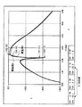
次に、実施例1と実施例2の平衡−不平衡変換回路に基づく周波数選択特性のシミュレーション結果について説明する。 Next, simulation results of frequency selection characteristics based on the balanced-unbalanced conversion circuit of the first and second embodiments will be described.
実施例1におけるLC並列共振回路7と実施例2におけるLC並列共振回路21のQ値を同じ値にするため、LC並列共振回路7におけるキャパシタ容量を4.05pF、インダクタンス値を0.85nHとし、LC並列共振回路21におけるキャパシタ容量を4.13pF(実施例1の1.02倍)、インダクタンス値を0.833nH(実施例1の1/1.02倍)とした。
In order to make the Q value of the LC parallel
図4は実施例1及び実施例2の周波数選択特性のシミュレーション結果を示す図である。
実施例1及び実施例2はそれぞれ2.4GHzの通過帯域を有すると共に、隣接する2.19GHzに減衰極が形成された周波数選択特性となっている。実施例1と実施例2を比較すると、コールド側にLC並列共振回路7を設けた実施例1は、ホット側にLC並列共振回路21を設けた実施例2よりも、2.19GHzにおける減衰量が3.1dB改善されていることが判る。これは、実施例2ではホット側にLC並列共振回路21を設けたので、ストレー容量によって回路構成が設計値からずれたことによるものと考えられる。
FIG. 4 is a diagram illustrating simulation results of frequency selection characteristics of the first and second embodiments.
Each of Example 1 and Example 2 has a passband of 2.4 GHz, and has frequency selection characteristics in which an attenuation pole is formed at the adjacent 2.19 GHz. Comparing Example 1 and Example 2, Example 1 in which the LC parallel
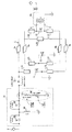
(実施例3)
図5は実施例3に係る平衡−不平衡変換回路の回路構成図である。
本実施例3に係る平衡−不平衡変換回路は、実施例1と同様にコールド側にLC並列共振回路7を設けると共に、不平衡端子2と第1の結合線路1との間にハイパスフィルタ31を設けたものである。
(Example 3)
FIG. 5 is a circuit configuration diagram of a balanced-unbalanced conversion circuit according to the third embodiment.
In the balanced-unbalanced conversion circuit according to the third embodiment, the LC parallel
ハイパスフィルタ31は、2つのLC並列共振回路32,33の中間接続点が、インダクタ34を介してグラウンドに接続されている。また、ハイパスフィルタ31の第1の結合線路側端部が、インダクタ35及びキャパシタ36からなるLC直列共振回路を介してグラウンドに接続されている。
In the high-
ここで、WLAN、WMAX等の無線通信では2.4〜3GHzが用いられる。一方、W-CDMA等の他の無線通信方式で使用する帯域(2.1GHz、1.9GHz等)が存在するので、それらを確実に減衰させる急峻なトラップ又はノッチフィルタを形成する必要がある。たとえば、2.17GHz付近を減衰させる要請がある。 Here, 2.4 to 3 GHz is used in wireless communication such as WLAN and WMAX. On the other hand, since there are bands (2.1 GHz, 1.9 GHz, etc.) used in other wireless communication systems such as W-CDMA, it is necessary to form a steep trap or notch filter that reliably attenuates them. For example, there is a request to attenuate around 2.17 GHz.
実施例3の平衡−不平衡変換回路では、2.4GHz以上を通過帯域とするハイパスフィルタ31を形成すると共に、2.17GHz及び1.9GHzでそれぞれ減衰極が形成されるように周波数選択特性に設計している。
なお、後段回路40はシミュレーションのために平衡端子5,6に接続したものである。
In the balanced-unbalanced conversion circuit of the third embodiment, the high-
The
(実施例4)
図6は実施例4に係る平衡−不平衡変換回路の回路構成図である。
本実施例4に係る平衡−不平衡変換回路は、実施例2と同様にホット側にLC並列共振回路21を設けると共に、不平衡端子2と第1の結合線路1との間にハイパスフィルタ31を設けたものである。ハイパスフィルタ31の周波数選択特性は基本的には実施例3と同様である。
Example 4
FIG. 6 is a circuit configuration diagram of a balanced-unbalanced conversion circuit according to the fourth embodiment.
In the balanced-unbalanced conversion circuit according to the fourth embodiment, an LC parallel
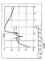
次に、実施例3と実施例4の平衡−不平衡変換回路に基づく周波数選択特性のシミュレーション結果について説明する。 Next, simulation results of frequency selection characteristics based on the balanced-unbalanced conversion circuit of the third and fourth embodiments will be described.
図7及び図8は実施例3及び実施例4の周波数選択特性のシミュレーション結果を示す図である。
図7に示すシミュレーションでは、実施例3におけるLC並列共振回路7と実施例4におけるLC並列共振回路21のQ値を同じ値にするため、LC並列共振回路7におけるキャパシタ容量を4.05pF、インダクタンス値を0.85nHとし、LC並列共振回路21におけるキャパシタ容量を4.13pF(1.02倍)、インダクタンス値を0.833nH(1/1.02倍)とした。また、実施例3の平衡−不平衡変換回路におけるハイパスフィルタ31のインダクタ35を2.7nH、キャパシタ36を3pFとし、実施例4の平衡−不平衡変換回路におけるハイパスフィルタ31のインダクタ35を4.05nH(実施例3の1.5倍)、キャパシタ36を2pF(実施例3の1/1.5倍)とした。
7 and 8 are diagrams showing simulation results of the frequency selection characteristics of the third and fourth embodiments.
In the simulation shown in FIG. 7, in order to make the Q values of the LC parallel
図7に示すように、通過帯域となっている2.4GHz帯に隣接する2.19GHzは実施例3及び実施例4ともに急峻に減衰しているが、コールド側にLC並列共振回路7を設けた実施例3の減衰量がホット側にLC並列共振回路21を設けた実施例4よりも3.8dB大きくなっている。また、インダクタ35及びキャパシタ36からなるLC直列共振回路により1.6GHzに減衰極が形成されている。
As shown in FIG. 7, although 2.19 GHz adjacent to the 2.4 GHz band which is the pass band is steeply attenuated in both the third and fourth embodiments, an LC
図8に示すシミュレーションでは、実施例3におけるLC並列共振回路7と実施例4におけるLC並列共振回路21は実施例3と同じ設定としている。また、実施例3及び実施例4の平衡−不平衡変換回路におけるハイパスフィルタ31のインダクタ35を2.7nH、キャパシタ36を3pFと同じ値に設定している。
In the simulation shown in FIG. 8, the LC
図8に示すように、実施例3では2.4GHzの通過帯域での減衰が−2.5dBであるのに対して、実施例4では2.4GHzの通過帯域での減衰が−5.1dBであり、実施例4は通過帯域のロスが実施例3よりも2.6dB増加していることが判る。
なお、本発明は上記実施の形態に限定されるものではない。例えば、必要性に応じて、通過帯域よりも高域側に減衰極を持たせるようにしても良い。
As shown in FIG. 8, in the third embodiment, the attenuation in the passband of 2.4 GHz is −2.5 dB, whereas in the fourth embodiment, the attenuation in the passband of 2.4 GHz is −5.1 dB. In Example 4, it can be seen that the loss of the passband is increased by 2.6 dB compared to Example 3.
The present invention is not limited to the above embodiment. For example, an attenuation pole may be provided on the higher frequency side than the pass band according to necessity.
1…第1の結合線路
2…不平衡端子
3…接地端子
4…第2の結合線路
5…第1の平衡端子
6…第2の平衡端子
7…帯域除去フィルタ
8、34、35…インダクタ
9、36…キャパシタ
11…第1のキャパシタ
12…第2のキャパシタ
13…後段回路
21…LC並列共振回路
31…ハイパスフィルタ
32、33…LC並列共振回路
DESCRIPTION OF
Claims (6)
前記第1の結合線路に接続された不平衡端子と、
前記第1の結合線路を介して前記不平衡端子に接続された接地端子と、
前記第1の結合線路に電磁結合した第2の結合線路と、
前記第2の結合線路に接続された第1の平衡端子と、
前記第2の結合線路を介して前記第1の平衡端子に接続された第2の平衡端子と、
前記第1の結合線路に対して直列に接続され当該第1の結合線路を伝搬する高周波信号中の所定帯域を除去する帯域除去フィルタと、
を具備したことを特徴とする平衡−不平衡変換回路。 A first coupled line;
An unbalanced terminal connected to the first coupled line;
A ground terminal connected to the unbalanced terminal via the first coupled line;
A second coupled line electromagnetically coupled to the first coupled line;
A first balanced terminal connected to the second coupled line;
A second balanced terminal connected to the first balanced terminal via the second coupled line;
A band elimination filter that is connected in series to the first coupling line and removes a predetermined band in a high-frequency signal propagating through the first coupling line;
A balanced-unbalanced conversion circuit comprising:
前記第2の結合線路における結合領域に対して並列に設けられた第2のキャパシタと、
を備え、
前記第1の結合線路と前記第1のキャパシタとが通過帯域で並列共振すると共に、前記第2の結合線路と前記第2のキャパシタとが前記通過帯域で並列共振することを特徴とする請求項1から請求項3のいずれかに記載の平衡−不平衡変換回路。 A first capacitor provided in parallel to a coupling region in the first coupling line;
A second capacitor provided in parallel to the coupling region in the second coupling line;
With
The first coupled line and the first capacitor resonate in parallel in a pass band, and the second coupled line and the second capacitor resonate in parallel in the pass band. The balanced-unbalanced conversion circuit according to any one of claims 1 to 3.
6. The inductor and capacitor constituting the band elimination filter, and the first and second coupled lines are formed in a multilayer substrate by a wiring pattern, according to any one of claims 3 to 5. Balance-unbalance conversion circuit.
Priority Applications (3)
| Application Number | Priority Date | Filing Date | Title |
|---|---|---|---|
| JP2008182565A JP4627791B2 (en) | 2008-07-14 | 2008-07-14 | Balance-unbalance conversion circuit |
| US12/492,504 US8018297B2 (en) | 2008-07-14 | 2009-06-26 | Balanced-unbalanced conversion circuit |
| TW098122639A TW201015851A (en) | 2008-07-14 | 2009-07-03 | Balanced-unbalanced conversion circuit |
Applications Claiming Priority (1)
| Application Number | Priority Date | Filing Date | Title |
|---|---|---|---|
| JP2008182565A JP4627791B2 (en) | 2008-07-14 | 2008-07-14 | Balance-unbalance conversion circuit |
Publications (2)
| Publication Number | Publication Date |
|---|---|
| JP2010021928A true JP2010021928A (en) | 2010-01-28 |
| JP4627791B2 JP4627791B2 (en) | 2011-02-09 |
Family
ID=41504631
Family Applications (1)
| Application Number | Title | Priority Date | Filing Date |
|---|---|---|---|
| JP2008182565A Expired - Fee Related JP4627791B2 (en) | 2008-07-14 | 2008-07-14 | Balance-unbalance conversion circuit |
Country Status (3)
| Country | Link |
|---|---|
| US (1) | US8018297B2 (en) |
| JP (1) | JP4627791B2 (en) |
| TW (1) | TW201015851A (en) |
Cited By (4)
| Publication number | Priority date | Publication date | Assignee | Title |
|---|---|---|---|---|
| CN103227616A (en) * | 2013-01-30 | 2013-07-31 | 王少夫 | Method for implementing bandstop filter with tunable bridge |
| KR20150135143A (en) * | 2014-05-23 | 2015-12-02 | 리니어 테크놀러지 코포레이션 | Broadband integrated rf/microwave/millimeter mixer with integrated balun(s) |
| WO2019003723A1 (en) * | 2017-06-30 | 2019-01-03 | 株式会社村田製作所 | Laminated balun |
| WO2019003722A1 (en) * | 2017-06-30 | 2019-01-03 | 株式会社村田製作所 | Balun |
Families Citing this family (4)
| Publication number | Priority date | Publication date | Assignee | Title |
|---|---|---|---|---|
| US8289085B2 (en) * | 2009-12-16 | 2012-10-16 | Auriga Measurement Systems, LLC | Amplifier circuit |
| US9166731B2 (en) * | 2013-05-23 | 2015-10-20 | Qualcomm Incorporated | Transformer with integrated notch filter |
| WO2018198602A1 (en) * | 2017-04-26 | 2018-11-01 | 株式会社村田製作所 | Balancing filter |
| WO2018198601A1 (en) * | 2017-04-26 | 2018-11-01 | 株式会社村田製作所 | Balance filter |
Citations (7)
| Publication number | Priority date | Publication date | Assignee | Title |
|---|---|---|---|---|
| JPS62222709A (en) * | 1986-03-25 | 1987-09-30 | Toyo Commun Equip Co Ltd | Antenna multicoupler circuit |
| JP2002217616A (en) * | 2001-01-15 | 2002-08-02 | Alps Electric Co Ltd | Balanced-to-unbalanced transformer |
| JP2002217670A (en) * | 2001-01-19 | 2002-08-02 | Toko Inc | Balun transformer |
| JP2003069360A (en) * | 2001-08-22 | 2003-03-07 | Kyocera Corp | Balun transformer |
| JP2005184245A (en) * | 2003-12-17 | 2005-07-07 | Mitsumi Electric Co Ltd | Coupler and high frequency module |
| JP2005333392A (en) * | 2004-05-19 | 2005-12-02 | Sony Corp | Resonator filter |
| JP2008061082A (en) * | 2006-09-01 | 2008-03-13 | Sony Corp | Balancing filter circuit and high frequency device fabricated thereby |
Family Cites Families (3)
| Publication number | Priority date | Publication date | Assignee | Title |
|---|---|---|---|---|
| JP2004274715A (en) | 2003-02-20 | 2004-09-30 | Murata Mfg Co Ltd | Balanced-to-unbalanced transformer circuit and multilayer balanced-to-unbalanced transformer |
| JP4433904B2 (en) * | 2004-07-01 | 2010-03-17 | ソニー株式会社 | Balun filter |
| US7683733B2 (en) * | 2008-02-04 | 2010-03-23 | Freescale Semiconductor, Inc. | Balun transformer with improved harmonic suppression |
-
2008
- 2008-07-14 JP JP2008182565A patent/JP4627791B2/en not_active Expired - Fee Related
-
2009
- 2009-06-26 US US12/492,504 patent/US8018297B2/en not_active Expired - Fee Related
- 2009-07-03 TW TW098122639A patent/TW201015851A/en unknown
Patent Citations (7)
| Publication number | Priority date | Publication date | Assignee | Title |
|---|---|---|---|---|
| JPS62222709A (en) * | 1986-03-25 | 1987-09-30 | Toyo Commun Equip Co Ltd | Antenna multicoupler circuit |
| JP2002217616A (en) * | 2001-01-15 | 2002-08-02 | Alps Electric Co Ltd | Balanced-to-unbalanced transformer |
| JP2002217670A (en) * | 2001-01-19 | 2002-08-02 | Toko Inc | Balun transformer |
| JP2003069360A (en) * | 2001-08-22 | 2003-03-07 | Kyocera Corp | Balun transformer |
| JP2005184245A (en) * | 2003-12-17 | 2005-07-07 | Mitsumi Electric Co Ltd | Coupler and high frequency module |
| JP2005333392A (en) * | 2004-05-19 | 2005-12-02 | Sony Corp | Resonator filter |
| JP2008061082A (en) * | 2006-09-01 | 2008-03-13 | Sony Corp | Balancing filter circuit and high frequency device fabricated thereby |
Cited By (9)
| Publication number | Priority date | Publication date | Assignee | Title |
|---|---|---|---|---|
| CN103227616A (en) * | 2013-01-30 | 2013-07-31 | 王少夫 | Method for implementing bandstop filter with tunable bridge |
| KR20150135143A (en) * | 2014-05-23 | 2015-12-02 | 리니어 테크놀러지 코포레이션 | Broadband integrated rf/microwave/millimeter mixer with integrated balun(s) |
| KR101688036B1 (en) | 2014-05-23 | 2016-12-20 | 리니어 테크놀러지 코포레이션 | Broadband integrated rf/microwave/millimeter mixer with integrated balun(s) |
| WO2019003723A1 (en) * | 2017-06-30 | 2019-01-03 | 株式会社村田製作所 | Laminated balun |
| WO2019003722A1 (en) * | 2017-06-30 | 2019-01-03 | 株式会社村田製作所 | Balun |
| JPWO2019003723A1 (en) * | 2017-06-30 | 2020-03-19 | 株式会社村田製作所 | Laminated balun |
| JPWO2019003722A1 (en) * | 2017-06-30 | 2020-04-09 | 株式会社村田製作所 | Balun |
| US10998876B2 (en) | 2017-06-30 | 2021-05-04 | Murata Manufacturing Co., Ltd. | Balun |
| US11005443B2 (en) | 2017-06-30 | 2021-05-11 | Murata Manufacturing Co., Ltd. | Multilayer balun |
Also Published As
| Publication number | Publication date |
|---|---|
| US8018297B2 (en) | 2011-09-13 |
| TW201015851A (en) | 2010-04-16 |
| JP4627791B2 (en) | 2011-02-09 |
| US20100007430A1 (en) | 2010-01-14 |
Similar Documents
| Publication | Publication Date | Title |
|---|---|---|
| JP4627791B2 (en) | Balance-unbalance conversion circuit | |
| JP3972810B2 (en) | Duplexer and communication device | |
| JP5322087B2 (en) | Frequency branch circuit | |
| JP6183461B2 (en) | High frequency module | |
| JP4697229B2 (en) | Elastic wave filter device | |
| US20160322956A1 (en) | High-frequency module | |
| JP2009033733A (en) | Antenna branching filter | |
| JP2004104799A (en) | Filter | |
| JP4428292B2 (en) | Triplexer circuit | |
| JP6822764B2 (en) | Demultiplexer | |
| KR20010051114A (en) | Integrated filter with improved i/o matching and method of fabrication | |
| JP2010141859A (en) | Diplexer and multiplexer | |
| TWI484753B (en) | High frequency module | |
| JP2008271187A (en) | Branch circuit | |
| WO2018012274A1 (en) | Ladder-type variable-frequency filter, multiplexer, high-frequency front end circuit, and communication terminal | |
| US20090167459A1 (en) | Duplexer | |
| JP6411288B2 (en) | Ladder filters, duplexers and modules | |
| JP2010154138A (en) | Layered multiplexer | |
| JP5804076B2 (en) | LC filter circuit and high frequency module | |
| JP2020028013A (en) | Filter and multiplexer | |
| JP2005286893A (en) | Passband flatness compensation circuit and filter | |
| JPH08274504A (en) | Filter device for high frequency | |
| JP5007499B2 (en) | Noise filter array | |
| JP2002217670A (en) | Balun transformer | |
| JP2008061082A (en) | Balancing filter circuit and high frequency device fabricated thereby |
Legal Events
| Date | Code | Title | Description |
|---|---|---|---|
| A131 | Notification of reasons for refusal |
Free format text: JAPANESE INTERMEDIATE CODE: A131 Effective date: 20100223 |
|
| A521 | Written amendment |
Free format text: JAPANESE INTERMEDIATE CODE: A523 Effective date: 20100413 |
|
| A131 | Notification of reasons for refusal |
Free format text: JAPANESE INTERMEDIATE CODE: A131 Effective date: 20100907 |
|
| A521 | Written amendment |
Free format text: JAPANESE INTERMEDIATE CODE: A523 Effective date: 20101018 |
|
| TRDD | Decision of grant or rejection written | ||
| A01 | Written decision to grant a patent or to grant a registration (utility model) |
Free format text: JAPANESE INTERMEDIATE CODE: A01 Effective date: 20101102 |
|
| A01 | Written decision to grant a patent or to grant a registration (utility model) |
Free format text: JAPANESE INTERMEDIATE CODE: A01 |
|
| A61 | First payment of annual fees (during grant procedure) |
Free format text: JAPANESE INTERMEDIATE CODE: A61 Effective date: 20101108 |
|
| FPAY | Renewal fee payment (event date is renewal date of database) |
Free format text: PAYMENT UNTIL: 20131119 Year of fee payment: 3 |
|
| R150 | Certificate of patent or registration of utility model |
Free format text: JAPANESE INTERMEDIATE CODE: R150 |
|
| LAPS | Cancellation because of no payment of annual fees |