JP2010016261A - Nitride semiconductor laser element - Google Patents
Nitride semiconductor laser element Download PDFInfo
- Publication number
- JP2010016261A JP2010016261A JP2008176167A JP2008176167A JP2010016261A JP 2010016261 A JP2010016261 A JP 2010016261A JP 2008176167 A JP2008176167 A JP 2008176167A JP 2008176167 A JP2008176167 A JP 2008176167A JP 2010016261 A JP2010016261 A JP 2010016261A
- Authority
- JP
- Japan
- Prior art keywords
- layer
- nitride semiconductor
- type
- semiconductor laser
- thickness
- Prior art date
- Legal status (The legal status is an assumption and is not a legal conclusion. Google has not performed a legal analysis and makes no representation as to the accuracy of the status listed.)
- Pending
Links
Images


Landscapes
- Semiconductor Lasers (AREA)
Abstract
Description
本発明は、光記憶メディア、照明およびディスプレイに用いられる窒化物半導体レーザ素子に関する。 The present invention relates to a nitride semiconductor laser device used for optical storage media, illumination, and displays.
近年、半導体レーザや発光ダイオード(LED:Light Emitting Diode)に用いられる発光素子として、青色または紫色の光を発する窒化物系半導体を発光層に用いた発光素子が検討されている。 In recent years, a light-emitting element using a nitride-based semiconductor that emits blue or violet light as a light-emitting layer has been studied as a light-emitting element used in a semiconductor laser or a light emitting diode (LED).
このうち半導体レーザに用いられる窒化物半導体レーザ素子は、製造プロセスおよび素子構造の両面から改善が進み、歩留りの改善等を通じて製造プロセス面での問題はほぼ解消されたものと考えられている。しかしながら、素子構造においては未だ改善途上にあり、より低出力で駆動でき、かつ高い発光効率を示す発光素子の開発が進められている。 Of these, nitride semiconductor laser elements used in semiconductor lasers are considered to have improved from both the manufacturing process and the element structure, and problems in the manufacturing process have been substantially solved through improvements in yield and the like. However, the device structure is still under improvement, and development of a light emitting device that can be driven at a lower output and that exhibits high light emission efficiency is underway.
従来の窒化物半導体レーザ素子は、n型GaN基板上にn型GaNバッファ層、n型AlGaNクラッド層、n型GaNガイド層、InGaN多重量子井戸活性層、p型AlGaN電流ブロック層、p型GaNガイド層、p型AlGaNクラッド層およびp型GaNコンタクト層をn型GaN基板側からこの順に形成され、上記InGaN多重量子井戸活性層を挟んで上下にn型AlGaNクラッド層およびp型AlGaNクラッド層を設けることによって、InGaN多重量子井戸活性層で発光した光を素子の外側に漏らさずに素子内に閉じ込め、素子内に光導波路を形成するという構造であった。 A conventional nitride semiconductor laser device includes an n-type GaN buffer layer, an n-type AlGaN cladding layer, an n-type GaN guide layer, an InGaN multiple quantum well active layer, a p-type AlGaN current blocking layer, and a p-type GaN on an n-type GaN substrate. A guide layer, a p-type AlGaN clad layer, and a p-type GaN contact layer are formed in this order from the n-type GaN substrate side, and an n-type AlGaN clad layer and a p-type AlGaN clad layer are arranged vertically above and below the InGaN multiple quantum well active layer. By providing, the light emitted from the InGaN multiple quantum well active layer was confined in the device without leaking outside the device, and an optical waveguide was formed in the device.
しかし、p型AlGaNクラッド層の屈折率がp型GaNコンタクト層の屈折率に比べて十分低くないために、InGaN多重量子井戸活性層で発光した光の一部がp型GaNコンタクト層側に漏れてしまい、発光素子内に十分に導波されずに発光効率(電流―光変換効率:SE Slope Efficiency)が低下するという問題があった。 However, since the refractive index of the p-type AlGaN cladding layer is not sufficiently lower than the refractive index of the p-type GaN contact layer, part of the light emitted from the InGaN multiple quantum well active layer leaks to the p-type GaN contact layer side. As a result, there is a problem in that light emission efficiency (current-light conversion efficiency: SE Slope Efficiency) is lowered without being sufficiently guided in the light emitting element.
そこで、上記問題を解決するため、特許文献1にはp型AlGaNクラッド層のドーパントにMgを用いることによって、p型AlGaNクラッド層の屈折率を低屈折率化し、もって光の漏れを防止する発光素子が提案されている。
Therefore, in order to solve the above problem,
特許文献1に記載されている窒化物半導体レーザ素子910の層構造は、図13に示されるように、厚さ400μmのn型GaN基板911上にn型GaN基板側から順に、厚さ2.5μmのn型Al0.05Ga0.95Nクラッド層913と、厚さ0.2μmのn型GaNガイド層914と、厚さ0.152μmのInGaN多重量子井戸活性層923と、厚さ0.012μmのp型Al0.15Ga0.85Nキャリアブロック層922と、厚さ0.2μmのp型GaNガイド層921と、厚さ0.6μmのp型Al0.05Ga0.95Nクラッド層924と、厚さ0.2μmのp型GaNコンタクト層924aと、p電極940とをこの順に含み、さらにp型Al0.05Ga0.95Nクラッド層924の表面は、誘導結合プラズマ(ICP:Inductive Coupled Plasma)エッチングによって、p型Al0.05Ga0.95Nクラッド層924の一部までエッチングされ、このエッチングされた部分に、厚さ200nmのSiO2層と厚さ50nmのTiO2層とからなるSiO2膜925とp電極940とが形成され、またn型GaN基板911の下面にn電極941が形成される。なお、p型Al0.15Ga0.85Nキャリアブロック層922、p型GaNガイド層921、p型Al0.05Ga0.95Nクラッド層924およびp型GaNコンタクト層924aのことをあわせてp型窒化物半導体層920という。
特許文献1に記載されている発明によれば、従来のp型AlGaNクラッド層を低屈折率化でき、光の漏れを効果的に防止することができる点で優れていたが、同時にこのMgでドープしたp型Al0.05Ga0.95Nクラッド層924を用いた素子は、発光効率を高効率に得るという点で以下のような2つの問題を有していた。
According to the invention described in
この素子の1つ目の問題は、p型窒化物半導体層920のドーパントに含まれるMgによってInGaN多重量子井戸活性層923で発光した光が強く吸収されてしまい、半導体レーザの発光効率が低下するという問題である。
The first problem of this element is that light emitted from the InGaN multiple quantum well
通常発光ダイオードに用いられる素子であれば、光を素子内に閉じ込める必要がないのでp型Al0.05Ga0.95Nクラッド層は含まれずp型窒化物半導体層も薄いため、たとえp型窒化物半導体層にMgが含まれていても、光吸収する層厚自体が薄くあまり問題とはならなかった。しかし、半導体レーザに用いられる素子は、素子内の導波路で光を共振させるためp型窒化物半導体層に含まれるMgの光吸収が非常に大きな問題となる。 In the case of an element normally used for a light emitting diode, it is not necessary to confine light in the element, and therefore, the p-type Al 0.05 Ga 0.95 N cladding layer is not included and the p-type nitride semiconductor layer is also thin. Even when Mg was contained in the layer, the thickness of the light-absorbing layer itself was small, and it was not a problem. However, since an element used in a semiconductor laser resonates light through a waveguide in the element, light absorption of Mg contained in the p-type nitride semiconductor layer becomes a very big problem.
さらに、もう1つの問題は、600〜800℃程度の比較的低温でp型窒化物半導体層920を形成すると、p型窒化物半導体層920が高抵抗化し、駆動電圧が高くなってしまい、もって半導体レーザの発光効率が低下するという問題である。
Furthermore, another problem is that when the p-type
つまり、p型窒化物半導体層920は1000℃以上の高温で成膜すれば、高抵抗化はされにくい傾向にあるが、1000℃以上の高温に熱するとInGaN多重量子井戸活性層923に含まれる結晶が熱によるダメージで結晶劣化を起こしてしまうため、600〜800℃程度で成膜する必要があった。このためp型窒化物半導体層920が高抵抗化してしまう問題を避けることができなかった。
That is, if the p-type
これは、440〜550nm程度の比較的長波長でレーザを発振させようとすると、InGaN多重量子井戸活性層923に含まれる井戸層のIn組成xを0.15以上0.3以下と比較的大きくする必要があるが、上記In組成xの場合、その後にp型窒化物半導体層920を作製する際の熱が大きく影響し、熱ダメージを受けやすくなる。このため、440〜550nm程度の比較的長波長でレーザを発振させようとすると、この熱ダメージが非常に問題であった。
This is because when the laser is oscillated at a relatively long wavelength of about 440 to 550 nm, the In composition x of the well layer included in the InGaN multiple quantum well
そこで、本発明は上記のような現状を鑑みてなされたものであって、より低出力で駆動でき、かつ発光効率のより高く、しかも440〜550nm程度の長波長の光を発光する窒化物半導体レーザ素子を提供することにある。 Therefore, the present invention has been made in view of the above situation, and is a nitride semiconductor that can be driven at a lower output, has higher luminous efficiency, and emits light having a long wavelength of about 440 to 550 nm. The object is to provide a laser element.
本発明者は、上記課題を解決すべく種々の検討を重ねた結果、p型窒化物半導体層を第二n型窒化物半導体層に代えることが上記目的に対して最も効果的であると考え、この知見の下、更に鋭意検討を重ねることによりついに本発明を完成したものである。 As a result of various studies to solve the above-mentioned problems, the present inventor considers that the replacement of the p-type nitride semiconductor layer with the second n-type nitride semiconductor layer is most effective for the above purpose. Based on this finding, the present invention was finally completed by further intensive studies.
本発明によれば、より低出力で駆動でき、かつ発光効率のより高く、しかも440〜550nm程度の長波長の光を発光する窒化物半導体レーザ素子を提供することができる。 According to the present invention, it is possible to provide a nitride semiconductor laser device that can be driven at a lower output, has higher luminous efficiency, and emits light having a long wavelength of about 440 to 550 nm.
すなわち、本発明の窒化物半導体レーザ素子は、基板上に、少なくとも、第一n型窒化物半導体層、p型窒化物半導体層、活性層および第二n型窒化物半導体層を基板側からこの順に含むことを特徴とする。 That is, the nitride semiconductor laser device of the present invention includes at least the first n-type nitride semiconductor layer, the p-type nitride semiconductor layer, the active layer, and the second n-type nitride semiconductor layer on the substrate from the substrate side. It is characterized by including in order.
上記基板または上記第一n型窒化物半導体層は、第一電極と接し、上記第二n型窒化物半導体層は、第二電極と接し、上記第一電極はアノード電極であり、第二電極はカソード電極であることが好ましい。 The substrate or the first n-type nitride semiconductor layer is in contact with the first electrode, the second n-type nitride semiconductor layer is in contact with the second electrode, the first electrode is an anode electrode, and the second electrode Is preferably a cathode electrode.
また、上記第二n型窒化物半導体層に対し上記活性層とは反対側に、導電性酸化物層を設けることが好ましい。また、基板または第一n型窒化物半導体層は、第一電極と接し、上記導電性酸化物層は、第二電極と接し、上記第一電極は、アノード電極であり、上記第二電極は、カソード電極であることが好ましい。また、上記活性層は、InxGa1-xN(0≦x≦1)からなる井戸層を含み、該井戸層のIn組成xは、0.15以上0.30以下であることが好ましい。 Moreover, it is preferable to provide a conductive oxide layer on the opposite side of the second n-type nitride semiconductor layer from the active layer. The substrate or the first n-type nitride semiconductor layer is in contact with the first electrode, the conductive oxide layer is in contact with the second electrode, the first electrode is an anode electrode, and the second electrode is A cathode electrode is preferable. The active layer includes a well layer made of In x Ga 1-x N (0 ≦ x ≦ 1), and the In composition x of the well layer is preferably 0.15 or more and 0.30 or less. .
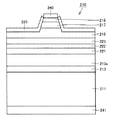
図1は本発明の代表的な窒化物半導体レーザ素子10の概略断面図である。図1に示されるように、本発明の窒化物半導体レーザ素子10は、基板11上に第一クラッド層13と第一n型ガイド層14とからなる第一n型窒化物半導体層12、AlyGa1-yN中間層30、p型ガイド層21とp型キャリアブロック層22とからなるp型窒化物半導体層20、活性層23、第二n型ガイド層16と第二クラッド層17とn型コンタクト層18とからなる第二n型窒化物半導体層15、電流狭窄絶縁膜25および第二電極40を有し、これらの層とは反対側の基板面には第一電極41を有する構造をしている。以下にこの構造に含まれる各層を説明する。
FIG. 1 is a schematic cross-sectional view of a typical nitride
<第一n型窒化物半導体層>
本発明の窒化物半導体レーザ素子10に含まれる第一n型窒化物半導体層12は、基板11上にある層であって、基板と接している、もしくは基板上にバッファ層や薄いアンドープ層(0.5μm以下)を挟んで形成されているn型の半導体層である。例えば第一クラッド層13と第一n型ガイド層14である。この第一n型窒化物半導体層12に用いられる材料は、ドーパントにSiを用いたAlxGayInzN(0≦x≦1;0≦y≦1;0≦z<1;x+y+z=1)を挙げることができる。また、第一n型窒化物半導体層12は、600〜800℃程度の比較的低温で形成することができる点、p型窒化物半導体層20と比べて低抵抗の層を形成することができる点、p型窒化物半導体層20と比べて結晶性の高い窒化物半導体を形成しやすい点等に特徴がある。
<First n-type nitride semiconductor layer>
The first n-type
また、第一n型窒化物半導体層12の基板11と接する面とは逆側の面の一部をp型クラッド層に代えることもできる。ただし、p型クラッド層を厚さ2μmよりも厚くすると、p型クラッド層に含まれるMgによる光吸収が大きくなるため好ましくなく、発光効率の観点からp型クラッド層に代える層厚は2μm以下が好ましい。以下に第一n型窒化物半導体層12に含まれる第一クラッド層13および第一n型ガイド層14を説明する。
Also, a part of the surface of the first n-type
(I)第一クラッド層
本発明の第一n型窒化物半導体層12に含まれる第一クラッド層13は、活性層23で発光した光のうち窒化物半導体成長面に対して垂直方向に広がる光を活性層周辺の素子内部に閉じ込める役割を果たす層であって、窒化物半導体層中を導波した光が分布している層である。活性層23で発光した光を素子内部に効果的に閉じ込めるためには、第一クラッド層13の屈折率は、活性層23および第一n型ガイド層14の屈折率より低い屈折率であることが望ましい。
(I) First Cladding Layer The
第一クラッド層13に用いられる材料としては、AlxGayInzN(0≦x<1;0≦y<1;0≦z<1;x+y+z=1)からなるn型窒化物半導体を挙げることができるが、第一クラッド層13をより低屈折率化するという観点から、特にAlyGa1-yN(0≦y≦0.1)を用いることが好ましい。一般にAlxGayInzNからなる窒化物半導体はInを含むほど屈折率は高くなり、Alを含むほど屈折率が低くなる傾向にあるからである。また、第一クラッド層13の層厚は、0.1μm以上10μm以下とすることができる。また、第一クラッド層の結晶構造は、AlGaNとGaNとの超格子構造であってもよいし、組成の異なるAlpGa1-pNとAlqGa1-qNとの超格子構造であってもよい。
As a material used for the
(II)第一n型ガイド層
本発明の第一n型窒化物半導体層12に含まれる第一n型ガイド層14に用いられる材料としては、AlyGa1-yN、AlxGayInzN、GaN等を挙げることができる。また、第一n型ガイド層14の層厚は、0.1μm以上10μm以下とすることができる。
(II) First n-type Guide Layer Materials used for the first n-
<p型窒化物半導体層>
本発明の窒化物半導体レーザ素子10に含まれるp型窒化物半導体層20は、p型ガイド層21とp型キャリアブロック層22とを含む層である。本発明の特徴は、活性層23の下側にp型窒化物半導体層が設けられ、第一n型窒化物半導体層とpn接合を有していることである。活性層23を成膜する前にp型窒化物半導体層20を設けることによって、活性層23成膜後の昇温を抑えることができ、活性層23の熱分解を効果的に防止することができる。このp型ガイド層21は0.01μm以上1μm以下の層厚であることが好ましく、p型キャリアブロック層22は1nm以上1000nm以下の層厚であることが好ましい。
<P-type nitride semiconductor layer>
The p-type
本発明のように活性層23を成膜する前にp型窒化物半導体層20を成膜すれば、活性層23の熱ダメージを気にすることなく、最適な成長温度および成膜条件でp型窒化物半導体層20を作製することができる。低抵抗のp型窒化物半導体層は高品質な結晶性が求められるが、従来の一般的な窒化物半導体レーザ、さらには、高In組成の活性層を有する長波長発光デバイスは、活性層成長後にp型窒化物半導体層を成膜するため、あまり高温で成膜することができなかった。しかしながら、本発明では1125℃程度の高温でp型窒化物半導体層を成膜することができるので、結晶性の高い非常に低抵抗なp型窒化物半導体層20を作製することができ、より高キャリア密度、光吸収の少ないp型窒化物半導体層20を作製することができる。このようにして良好に活性層に効率よくホールを注入することができるようになり、信頼性およびレーザ発振後の発光効率(スロープ効率)を改善する。
If the p-type
また、p型窒化物半導体層20のドーパントに用いられるMgは深いエネルギー準位を形成することから、p型窒化物半導体層20は高抵抗になりやすく、特にAlを含むp型窒化物半導体層20は特に高抵抗になりやすい。このため、p型窒化物半導体層20の厚みを厚くするほど、直列抵抗が大きくなるため駆動電圧が上がり、発光効率を低下させてしまう。したがって、p型窒化物半導体層20はなるべく薄膜で成膜することが好ましい。
Further, Mg used as the dopant of the p-type
<pn接合>
本発明の窒化物半導体レーザ素子10は、活性層23にpn接合が含まれている以外に、基板11と活性層23との間にもpn接合が含まれていることを特徴とする。たとえば図1において第一n型ガイド層14とp型ガイド層21の間にpn接合が含まれている。このpn接合の方向は、活性層のpn接合に順方向にバイアスしたとき、すなわち第一電極41に正のバイアス、第二電極40に負のバイアスを印加したときに、基板11と活性層23との間にあるpn接合に逆方向にバイアスする方向にpn接合が設けられる。ここで、レーザ発振させる場合には、第一電極41に正のバイアスを印加させ、第二電極40に負のバイアスを印加させることになる。
<Pn junction>
The nitride
ただし、基板11と活性層23との間にあるpn接合に逆方向にバイアスするようにpn接合が設けられている場合、pn接合界面の空乏層の幅が広がってしまうためトンネル電流が流れにくい。しかし、以下の(I)(II)に示す方法をとることによって、もってトンネル電流を流しやすくすることができる。
However, when a pn junction is provided so as to bias the pn junction between the
(I)1つ目の方法は、図2に示されるように、第一n型ガイド層14とp型ガイド層21との間にあるpn接合の界面近傍に、Siのドーピング量を多くしたn+ドープ層14aと、Mgのドーピング量を多くしたp+ドープ層21aとを設けるという方法である。このようにpn接合の界面近傍にn+ドープ層14aおよびp+ドープ層21aを設けることによって、第一n型ガイド層14とp型ガイド層21との間の空乏層の幅が狭くなり、トンネル電流が流れやすくなる。このようにn+ドープ層14aおよびp+ドープ層21aを設ける場合、n+ドープ層14aにおけるキャリア濃度およびp+ドープ層21aにおけるキャリア濃度は、いずれも5×10¹⁸/cm3以上であることが好ましい。また、このn+ドープ層14aおよびp+ドープ層21aの層厚は、pn接合界面の数原子程度であってもよいし、10〜30nm程度の厚さであってもよい。
(I) In the first method, as shown in FIG. 2, the Si doping amount is increased in the vicinity of the pn junction interface between the first n-
<AlyGa1-yN中間層>
(II)もう1つの方法は、図1に示されるように第一n型ガイド層14とp型ガイド層21との間にAlyGa1-yN中間層30を設けるという方法である。このようにpn接合の界面にAlyGa1-yN中間層30を設けることによって、c面の窒化物半導体で格子不整合による格子歪が起こり、この格子歪からピエゾ電界による自発分極が発生し、伝導帯のバンドエネルギー、価電子帯のバンドエネルギーを歪ませる効果がある。この歪みによって空乏層の幅が狭くなり、逆方向にバイアスしたときにトンネル電流が流れやすくなる。ここで、この格子不整合による格子歪には、圧縮応力の方向による歪みと引っ張り応力の方向による歪みとの2種類の歪みがあるが、この2種の歪みのうち、空乏層の幅を狭くするように歪ませる方の歪みを適宜選択する必要がある。本発明においては、たとえばAlNを用いることによって、格子不整合による格子歪から空乏層の幅を狭くでき、トンネル電流を流しやすくできる。
<Al y Ga 1-y N intermediate layer>
(II) Another method is to provide an Al y Ga 1-y N intermediate layer 30 between the first n-
また、AlyGa1-yN中間層30の層厚は、0.5〜100nmとすることができる。また、AlyGa1-yN中間層30には、AlyGa1-yN(0≦y≦1)を好適に用いることができ、AlNを用いることが特に好ましい。本発明においてpn接合には、上記に示したAlyGa1-yN中間層が形成されていても良いし、AlN、InGaN、InN、AlInGaN等の窒化物半導体が0.5〜100nmの厚さで形成されていても良い。AlyGa1-yN中間層は、n型伝導またはp型伝導を示すように不純物がドーピングされていてもよいし、アンドープであってもよい。 The layer thickness of the Al y Ga 1-y N intermediate layer 30 can be set to 0.5 to 100 nm. Further, Al y Ga 1-y N (0 ≦ y ≦ 1) can be suitably used for the Al y Ga 1-y N intermediate layer 30, and it is particularly preferable to use AlN. In the present invention, the above-described Al y Ga 1-y N intermediate layer may be formed in the pn junction, and nitride semiconductors such as AlN, InGaN, InN, and AlInGaN have a thickness of 0.5 to 100 nm. It may be formed. The Al y Ga 1-y N intermediate layer may be doped with impurities so as to exhibit n-type conduction or p-type conduction, or may be undoped.
<第二n型窒化物半導体層>
本発明の窒化物半導体レーザ素子10に含まれる第二n型窒化物半導体層15は、活性層23からみて基板11とは反対側に位置することを特徴とする。
<Second n-type nitride semiconductor layer>
The second n-type
従来の窒化物半導体レーザ素子は、活性層23を形成した後に1000℃を超える高温でp型窒化物半導体層を成膜すると、Inを含む活性層が分解するという問題があった。ところが、本発明によればInを含む活性層を形成した後にp型窒化物半導体層を成膜することなく、Inの熱分解が起こりにくい600〜800℃程度の比較的低温で第二n型窒化物半導体層を成膜できることから、In組成xが0.15〜0.4程度の活性層を含んでいても熱分解を生じることなく窒化物半導体レーザ素子を製造できる。
The conventional nitride semiconductor laser device has a problem that when the p-type nitride semiconductor layer is formed at a high temperature exceeding 1000 ° C. after the
また、従来の窒化物半導体レーザ素子910に用いられるp型窒化物半導体層920は、本質的に低抵抗となりにくいことから直列抵抗が高くなり窒化物半導体レーザ素子の駆動電圧が増大しやすいという問題もあった。しかし、本発明のように活性層23の上に低抵抗な第二n型窒化物半導体層15を用いれば第二n型窒化物半導体層15の導電性の高さから、窒化物半導体レーザ素子10の駆動電圧も低くすることができる。また、第二n型窒化物半導体層15の上に後述する導電性酸化物層をさらに設けた場合でも、電気抵抗はそれほど増大しないため窒化物半導体レーザ素子10の駆動電圧は導電性酸化物層を設けなかった場合とほとんど変わらない。
In addition, since the p-type
さらに、従来の窒化物半導体レーザ素子910は、p型窒化物半導体層920上にp電極940を作製していたため、1つの窒化物半導体レーザ素子の両端にp電極940とn電極941とを有していた。しかし、本発明によればp電極940を作製する必要がなく、窒化物半導体レーザ素子の両端をn電極のみで作製することができ、しかも2つのn電極は同一の材料でも成膜できることから、電極の蒸着する際の生産性を向上できるとともに、コストダウンも可能となる。なお、この2つのn電極に用いられる材料は、同一の材料に限られるものではなく、別々の材料を用いてもよい。
Further, since the conventional nitride
本発明の窒化物半導体レーザ素子10に用いられる第二n型窒化物半導体層15は、第二n型ガイド層16と第二クラッド層17とn型コンタクト層18とのうちのいずれか1層以上を含む層であり、このような第二n型窒化物半導体層15に用いられる材料としては、ドーパントにSiを用いたAlxGayInzN(0≦x≦1;0≦y≦1;0≦z≦1;x+y+z=1)、すなわちn型窒化物半導体を挙げることができる。
The second n-type
また、第二n型窒化物半導体層15はレーザーアブレーション(PLD:Pulsed Laser Deposition)によって成膜することもできる。PLD法は高エネルギー紫外線レーザによる原料の昇華を利用した成長手法であり、昇華した材料の作り出す局所的な強い非平衡場により窒素ガスが解離・反応するため、III族窒化物半導体の低温・窒素雰囲気中で成長させることができる。PLD法では、KrFエキシマレーザーをエネルギー密度3J/cm2、繰り返し周波数10〜15Hzで原料となるターゲット(Ga、Al、In、AlN、GaN、InNなど)に照射する。このレーザ照射によりターゲット原料は瞬間的に昇華し、プルームと呼ばれる一種のプラズマ状態となって雰囲気ガス分子(窒素ガス、酸素ガス等)との衝突を繰り返した後、基板上へ到達して薄膜を形成する。窒素源として窒素ガスを10-5〜10-1Torrの圧力で導入する。この方法によれば、室温で高品質な窒化物半導体を作製でき、熱による活性層のダメージを著しく低減することできる。
The second n-type
また、第二n型窒化物半導体層15は、パルススパッタ(PSD:Pulsed Sputter Deposition)法によって成膜することもできる。活性層を成膜した後、第二n型窒化物半導体層をPSD法で成膜することにより、第二n型窒化物半導体層15をよりいっそう低温で成膜することができ、もって活性層23への熱ダメージを著しく低減することができる。PSD法によって全ての第二n型窒化物半導体層を成膜してもよいし、一部のみを成膜してもよい。
The second n-type
(I)第二n型ガイド層
本発明の第二n型窒化物半導体層15に含まれる第二n型ガイド層16は、第二クラッド層17と接する層である。この第二n型ガイド層16に用いられる材料としては、AlxGayInzN(0≦x≦1;0≦y≦1;0≦z≦1;x+y+z=1)を挙げることができる。また、第二n型ガイド層16の層厚は、0.01μm以上1μm以下とすることができるが、後述するリッジストライプ部70の形成に際して一部がエッチング等の方法により取り除かれ、図1に示すように第二n型ガイド層のエッチングにより除去された部分の層厚はdとなる。
(I) Second n-type Guide Layer The second n-
(II)第二クラッド層
本発明の第二n型窒化物半導体層15に含まれる第二クラッド層17は、活性層23で発光した光のうち窒化物半導体成長面に対して垂直方向に広がる光を活性層23付近の半導体内部に閉じ込める役割を果たしている層である。この第二クラッド層17は、活性層23および第二n型ガイド層16の屈折率より低い屈折率を有していることが好ましい。本発明においては、高抵抗で知られるp型AlGaNクラッド層を用いずに、第二クラッド層17で光閉じ込めを行なうため、従来の窒化物半導体レーザ素子よりも駆動電圧を低減することができる。ここで、第二クラッド層17に用いられる材料としては、AlxGayInzN(0≦x≦1;0≦y≦1;0≦z<1;x+y+z=1)、AlyGa1-yN(0≦y≦0.1)、GaN等を挙げることができるが、第二クラッド層17をより低屈折率化するという観点から、AlyGa1-yN(0≦y≦0.1)を用いることがより好ましい。また第二クラッド層17にGaN材料を用いる場合、活性層23との屈折率差が十分でなく、光閉じ込め効果が弱くなることが懸念されるため、第二クラッド層17の代わりに後述する導電性酸化物層を用いることもできるし、第二クラッド層17の上にさらに導電性酸化物層を含むこともできる。
(II) Second Cladding Layer The
また、第二クラッド層17の結晶構造は、AlGaNとGaNとの超格子構造であってもよいし、組成の異なるAlpGa1-pNとAlqGa1-qNとの超格子構造であってもよい。また、第二クラッド層17の層厚は0.01μm以上10μm以下であることが好ましく、0.2μm以上8μm以下であることがより好ましい。
The crystal structure of the
(III)n型コンタクト層
本発明の第二n型窒化物半導体層15に含まれるn型コンタクト層18は、第二クラッド層17と第二電極40との間に位置する層である。このn型コンタクト層18の層厚は、0.01μm以上1μm以下とすることができる。
(III) n-type Contact Layer The n-
<基板>
本発明の窒化物半導体レーザ素子の基板11に用いられる材料としては、結晶構造が六方晶形の結晶構造を有する材料を特に好ましく用いることができ、このような材料としてたとえば、窒化物半導体基板、サファイア基板、SiC基板等を挙げることができる。また、基板11と基板11上に形成される窒化物半導体層との格子整合性を高めるという観点から、基板11には窒化物半導体基板を用いることが好ましく、特にn型の窒化物半導体基板を用いることが好ましい。
<Board>
As a material used for the
また、窒化物半導体基板を用いる場合、その窒化物半導体基板の組成は、AlxGayInzN(0≦x≦1;0≦y≦1;0≦z<1;x+y+z=1)を有するものを用いることができ、具体的にはGaN、AlGaN、AlN、InGaN等を用いることができる。また、この窒化物半導体基板の六方晶形が保たれる範囲であれば、窒化物半導体基板に含まれるN元素の一部を、As、PまたはSbからなる群より選択された少なくとも1種の元素に置換することもできる。ここで、「N元素の一部」とは、窒化物半導体基板AlxGayInzNに含まれるNのうち、10%以下のNのことをいう。 Further, when a nitride semiconductor substrate is used, the composition of the nitride semiconductor substrate is Al x Ga y In z N (0 ≦ x ≦ 1; 0 ≦ y ≦ 1; 0 ≦ z <1; x + y + z = 1). In particular, GaN, AlGaN, AlN, InGaN, or the like can be used. If the hexagonal crystal shape of the nitride semiconductor substrate is maintained, at least one element selected from the group consisting of As, P, or Sb may be used as a part of the N element contained in the nitride semiconductor substrate. Can also be substituted. Here, “a part of the N element” means 10% or less of N in N contained in the nitride semiconductor substrate Al x Ga y In z N.
このような基板の層厚は、10μm以上1000μm以下であることが好ましく、さらに好ましくは100μm以上800μm以下であり、理想的には200μm以上600μm以下である。 The layer thickness of such a substrate is preferably 10 μm or more and 1000 μm or less, more preferably 100 μm or more and 800 μm or less, and ideally 200 μm or more and 600 μm or less.
<活性層>
本発明の窒化物半導体レーザ素子10に用いられる活性層23は、バリア層と井戸層とを交互に積層した積層体を有し、さらにこの積層体を緩衝層によって、両側から挟んだ構造をした多重量子井戸活性層構造であり、600〜800℃の温度で成膜することが好ましい。バリア層には、InxGa1-xNが用いられ、井戸層はバリア層よりIn組成の高い、InxGa1-xNが用いられる。また、活性層23の層厚は、上述のバリア層と井戸層との層厚の合計で表すことができ、0.01μm以上1μm以下であることが好ましい。
<Active layer>
The
また、本発明の活性層とp型窒化物半導体層との間および活性層と第二n型窒化物半導体層との間に、AlxGayInzN(0≦x<1;0≦y≦1;0≦z<1;x+y+z=1)からなる緩衝層を設けることが好ましい。この緩衝層の組成は、InxGa1-xN(In組成x:0≦x≦0.1)であることが好ましい。また、In組成の多い(In組成0.15以上0.3以下)活性層23を成膜する際に緩衝層を形成すると、井戸層の結晶性を向上させることができる。これは、井戸層にかかる格子不整合から引き起こされる大きな歪を緩衝層によって軽減することができるためと考えられる。
Further, between the active layer and the p-type nitride semiconductor layer of the present invention and between the active layer and the second n-type nitride semiconductor layer, Al x Ga y In z N (0 ≦ x <1; 0 ≦ It is preferable to provide a buffer layer of y ≦ 1; 0 ≦ z <1; x + y + z = 1). The composition of the buffer layer is preferably In x Ga 1-x N (In composition x: 0 ≦ x ≦ 0.1). Further, when the buffer layer is formed when forming the
ここで、緩衝層の層厚は、1nm以上0.4μm以下が好ましい。また、活性層とp型窒化物半導体層の間に設けられる緩衝層は、ノンドープまたはp型ドーピングであることが好ましく、活性層と第二n型窒化物半導体層との間に設けられる緩衝層は、ノンドープまたはn型ドーピングであることが好ましい。ただし、緩衝層を設けなくても本発明の効果と同様の効果を得ることができる。 Here, the thickness of the buffer layer is preferably 1 nm or more and 0.4 μm or less. The buffer layer provided between the active layer and the p-type nitride semiconductor layer is preferably non-doped or p-type doped, and the buffer layer provided between the active layer and the second n-type nitride semiconductor layer. Is preferably non-doped or n-type doped. However, the same effects as those of the present invention can be obtained without providing a buffer layer.
また、活性層23に用いられる材料は、アルミニウム、インジウムおよびガリウムからなる群から選択された少なくとも1種の3族元素と5族元素である窒素との化合物を用いることが好ましく、組成式で表すとAlxGayInzN(0≦x≦1;0≦y≦1;0≦z≦1;x+y+z=1)となる。すなわち、後述する実施例には、InxGa1-xNを用いた活性層のみを説明しているが、これに限られるものではなく活性層にAlを含めた混晶を用いることもできる。
The material used for the
また、活性層23に含まれる、バリア層および井戸層は、いずれもノンドープInxGa1-xN(0<x≦1)からなる層である。このバリア層の層厚は1nm以上100nm以下であることが好ましく、1nm以上40nm以下が特に好ましい。1nmより薄いとキャリアのバリア層としての効果を得られないため好ましくなく、40nmより厚いと、井戸層間の距離が離れすぎてしまい、井戸層にキャリアが不均一に注入される可能性があるため好ましくない。
Further, the barrier layer and the well layer included in the
また、井戸層の層厚は0.5nm以上10nm以下が好ましい。0.5nmより薄いと、井戸層が均一に形成されないため好ましくなく、10nmより厚くなると、格子不整合による歪からInの凝集が起こりやすくなるため好ましくない。更に井戸層数は1層から3層程度を形成することが好ましい。また、本発明の窒化物半導体レーザ素子から発振されるレーザ光の波長は活性層23の井戸層の混晶比によって、たとえば440nm〜550nmの範囲で適宜調節することができる。また、活性層23に含まれる井戸層のIn組成xは、0.15〜0.3であることが好ましい。活性層のIn組成xが0.15の時、レーザの発振波長は440nm程度となり、In組成xが0.3の時、レーザの発振波長は550nm程度となる。なお、In組成が増加すると線形的に発振波長も長波長化する。
Further, the thickness of the well layer is preferably 0.5 nm or more and 10 nm or less. If it is thinner than 0.5 nm, the well layer is not formed uniformly, and it is not preferable. If it is thicker than 10 nm, it is not preferable because In aggregation is likely to occur due to strain due to lattice mismatch. Furthermore, it is preferable to form about 1 to 3 well layers. Further, the wavelength of the laser light oscillated from the nitride semiconductor laser element of the present invention can be appropriately adjusted within a range of 440 nm to 550 nm, for example, depending on the mixed crystal ratio of the well layer of the
本発明の窒化物半導体レーザ素子において、活性層23と第二n型ガイド層16との間に、キャリアブロック層(図示せず)を設けることが好ましい。活性層23を成膜した後に低温で第二n型ガイド層16を成膜すると、第二n型ガイド層16の結晶性が粗悪になるため活性層23(特にIn組成の大きい井戸層)を十分に保護できない場合がある。しかしながら、活性層23と第二n型ガイド層16との間にキャリアブロック層を設けることによって、活性層23からオーバーフローした電子のキャリアブロックを行なうことができるし、活性層23をより保護することもできる。このキャリアブロック層の層厚はたとえば10nmとすることができる。
In the nitride semiconductor laser device of the present invention, it is preferable to provide a carrier block layer (not shown) between the
このキャリアブロック層に用いられる材料としては、たとえばAlxGayInzN(0≦x≦1;0≦y≦1;0≦z<1;x+y+z=1)、AlpGa1-pN(0<p≦1)等を用いることができる。ここで、キャリアブロック層にAlpGa1-pNを用いる場合、Al組成pは0より大きいことが好ましいが、Al組成pを大きくしすぎると格子不整合によるクラックが生じることから好ましくない。このようなAl組成pとしてはたとえば0.18程度とすることができる。なお、キャリアブロック層は、n型にドーピングされていることが好ましいが、ノンドープであってもよい。 As a material used for this carrier block layer, for example, Al x Ga y In z N (0 ≦ x ≦ 1; 0 ≦ y ≦ 1; 0 ≦ z <1; x + y + z = 1), Al p Ga 1-p N (0 <p ≦ 1) or the like can be used. Here, when Al p Ga 1-p N is used for the carrier block layer, the Al composition p is preferably larger than 0. However, if the Al composition p is too large, cracks due to lattice mismatching are not preferable. Such an Al composition p can be set to about 0.18, for example. The carrier block layer is preferably n-type doped, but may be non-doped.
また、格子不整合から生じるクラックを緩和するという観点と、さらに低温で成膜できるという観点とからすれば、キャリアブロック層に用いられる材料にはAlxGayInzN(0<x<1;0<y<1;0<z<1;x+y+z=1)を用いることが好ましい。この場合、In組成zが0より大きく0.3より小さいことが好ましく、0.3より大きくなると層分離を起こしてしまうという問題、およびキャリアブロック層の再蒸発が起こるという問題があるため好ましくない。また、Al組成xは0より大きいことが好ましく、たとえば0.18程度とすることができる。 Further, from the viewpoint of alleviating cracks caused by lattice mismatch and from the viewpoint of being able to form a film at a lower temperature, the material used for the carrier block layer may be Al x Ga y In z N (0 <x <1). 0 <y <1; 0 <z <1; x + y + z = 1) is preferably used. In this case, it is preferable that the In composition z is larger than 0 and smaller than 0.3, and if it exceeds 0.3, there is a problem that layer separation occurs and a problem that re-evaporation of the carrier block layer occurs. . The Al composition x is preferably larger than 0, and can be about 0.18, for example.
また、緑色光や赤色光のような可視光の中では長波長領域の光を発する窒化物半導体レーザ素子を製造するためには、活性層のIn組成xが0.15〜0.3の高いIn含有量の活性層が必要とされる。しかし、In組成xが0.15〜0.3程度の高いIn組成の活性層は赤色や緑色の光を発光する活性層の熱分解温度はかなり低いため、従来の製造方法のように活性層を成膜した後に1000℃以上の高温状態でp型窒化物半導体層を成膜すると、活性層が熱によるダメージで結晶劣化を起こすことから、緑色光や赤色光を発する窒化物半導体レーザ素子の製造が困難であった。このInを含む窒化物半導体結晶の熱分解温度の低さを表す例として、たとえばInNは600〜700℃で熱分解が起こる程度にInを含む活性層の熱分解温度は低い。 Further, in order to manufacture a nitride semiconductor laser device that emits light in a long wavelength region in visible light such as green light and red light, the In composition x of the active layer is as high as 0.15 to 0.3. An active layer with an In content is required. However, an active layer having a high In composition with an In composition x of about 0.15 to 0.3 has a considerably low thermal decomposition temperature of the active layer emitting red or green light. When the p-type nitride semiconductor layer is formed at a high temperature of 1000 ° C. or higher after the film is formed, the active layer causes crystal degradation due to heat damage. Therefore, the nitride semiconductor laser element that emits green light or red light is used. Manufacturing was difficult. As an example showing the low thermal decomposition temperature of a nitride semiconductor crystal containing In, for example, the thermal decomposition temperature of an active layer containing In is so low that InN undergoes thermal decomposition at 600 to 700 ° C.
ところが、本発明で作製された窒化物半導体レーザ素子10は、活性層23を成膜した後、p型窒化物半導体層を成膜することなく、600〜900℃程度の比較的低温で第二n型窒化物半導体層15を成膜し、この後の製造過程においても900℃を超える温度に昇温することがないので、In組成xは、0.15以上を含む活性層を用いても熱分解することなく窒化物半導体レーザ素子を製造することができるし、In組成xは、0.2以上を含む活性層であっても熱分解することなく窒化物半導体レーザ素子を製造することもできる。
However, the nitride
<基板の主面>
本発明に用いられる基板11の主面には、c面{0001}、A面{11−20}、R面{1−102}、M面{1−100}、{1−101}面および{11−22}面から選択された少なくとも1つの面を用いることができる。この基板上に形成されるp型窒化物半導体層を低抵抗にするという観点から、c面を主面とする基板を用いることが好ましい。
<Main surface of substrate>
The principal surface of the
なお、結晶面を表わす場合に、本来であれば所要の数字の上にバーを付した表現をするべきであるが、表現手段に制約があるため、本明細書においては、所要の数字の上にバーを付す表現の代わりに、所要の数字の前に「−」を付して表現している。 In addition, when expressing a crystal plane, it should be expressed by adding a bar on a required number. However, because there are restrictions on expression means, in this specification, the required number Instead of the expression with a bar, the symbol “-” is added in front of the required number.
また、基板の主面に対するオフ角度が0.1〜2°であれば、その表面モフォロジーが良好であるため面内の層厚分布を小さくすることができる。したがって、たとえば基板の主面がM面{1−100}の場合、M面内のc軸方向のオフ角度が0.1〜2°に傾いていれば、表面モフォロジーが良好であるため面内の層厚分布を小さくすることができる。 Moreover, if the off angle with respect to the main surface of the substrate is 0.1 to 2 °, the surface morphology is good, so that the in-plane layer thickness distribution can be reduced. Therefore, for example, when the main surface of the substrate is the M plane {1-100}, if the off-angle in the c-axis direction in the M plane is inclined by 0.1 to 2 °, the surface morphology is good and the in-plane The layer thickness distribution can be reduced.
ここで、基板の主面に対するオフ角度が0.1°未満であれば、面内の層厚分布が大きくなる虞があり好ましくない。また、基板の主面に対するオフ角度が2°より大きくなると、表面のステップ形状が顕著になり、面内の層厚分布が大きくなる虞があり好ましくない。 Here, if the off angle with respect to the main surface of the substrate is less than 0.1 °, the in-plane layer thickness distribution may increase, which is not preferable. Further, when the off angle with respect to the main surface of the substrate is larger than 2 °, the step shape of the surface becomes remarkable, and the in-plane layer thickness distribution may be increased, which is not preferable.
<導電性酸化物層>
本発明の窒化物半導体レーザ素子に用いられる導電性酸化物層は、窒化物半導体層上に形成される層であって、高屈折率を有する材料からなる層である。また、導電性酸化物層に用いられる材料としては、錫ドープ酸化インジウム(ITO:Indium Tin Oxide)、アルミニウムドープ酸化亜鉛(ZnO:Al)、ガリウムドープ酸化亜鉛(ZnO:Ga)フッ素ドープ酸化錫(SnO2:F)、ニオビウム(Nb)がドープされた二酸化チタン、β−Ga2O3等の導電性酸化物もしくは分子線エピキタシー(MBE:Molecular Beam Epitaxy)法または有機金属気相成長(MOCVD:Metal Organic Chemical Vapor Deposition)法で作製されたn型の酸化亜鉛(ZnO)を挙げることができる。
<Conductive oxide layer>
The conductive oxide layer used in the nitride semiconductor laser device of the present invention is a layer formed on the nitride semiconductor layer and made of a material having a high refractive index. In addition, as a material used for the conductive oxide layer, tin-doped indium oxide (ITO), aluminum-doped zinc oxide (ZnO: Al), gallium-doped zinc oxide (ZnO: Ga) fluorine-doped tin oxide ( SnO 2 : F), titanium dioxide doped with niobium (Nb), conductive oxide such as β-Ga 2 O 3 or molecular beam epitaxy (MBE) method or metal organic chemical vapor deposition (MOCVD) An n-type zinc oxide (ZnO) produced by the Metal Organic Chemical Vapor Deposition method can be mentioned.
また、この導電性酸化物層は、EB蒸着法、スパッタ成膜法、MBE法、MOCVD法等によって成膜することができ、これらの方法を用いれば300℃以下の比較的低温で導電性酸化物層を成膜することができる。このことから活性層23の熱分解を避けつつ、導電性酸化物層を成膜することができるというメリットがある。
The conductive oxide layer can be formed by EB vapor deposition, sputter deposition, MBE, MOCVD, etc., and these methods can be used to conduct conductive oxidation at a relatively low temperature of 300 ° C. or lower. A physical layer can be formed. Therefore, there is an advantage that the conductive oxide layer can be formed while avoiding thermal decomposition of the
また、GaNを用いる第二クラッド層17は、AlGaNを用いる第二クラッド層の屈折率と比べて屈折率が高くなるため、第二クラッド層17の光閉じ込め効果が弱くなる。このような場合に、第二クラッド層17の上にさらに導電性酸化物層を設ければ、第二クラッド層17と導電性酸化物層との屈折率差がより大きくなり、第二クラッド層17の光閉じ込め効果を上げることができると考えられる。また、第二クラッド層17の代わりに導電性酸化物層を用いることもできる。
Moreover, since the refractive index of the
<電流狭窄絶縁膜>
本発明の窒化物半導体レーザ素子に用いられる電流狭窄絶縁膜25は、第二n型ガイド層16と第二クラッド層17とに接触するように設けられる膜であって、絶縁性を有する膜である。
<Current confinement insulating film>
The current
この電流狭窄絶縁膜25に用いられる材料としては、たとえば、シリコンの酸化物、アルミニウムの酸化物、ジルコニアの酸化物、チタンの酸化物、タンタルの酸化物、シリコンの酸窒化物、アルミニウムの酸窒化物、ジルコニアの酸窒化物、チタンの酸窒化物、タンタルの酸窒化物、シリコンの窒化物、アルミニウムの窒化物、ノンドープAlN、ノンドープAlGaN、ノンドープInAlN、p型AlN、p型AlGaN、p型InAlN等の材料のうちから選択された少なくとも1種を挙げることができる。ただし、p型AlN、p型AlGaNまたはp型InAlNを用いる場合、これらに含まれるMgが光吸収するため、Mgのドープ量が少ない方が好ましく、ノンドープであることがより好ましい。
Examples of the material used for the current
また、電流狭窄絶縁膜25は、従来より公知の方法で成膜することができ、たとえばEB蒸着法、スパッタ法、MOCVD法、MBE法等によって成膜することができる。また、電流狭窄絶縁膜25は、単層構造に限られるものではなく多層構造であってもよい。
The current
電流狭窄絶縁膜25の層厚は、6〜1000nmであることが好ましく、6〜500nmであることがより好ましい。層厚が6nm未満の場合は面内に均一な膜を形成しにくいため、電流がリークして電流狭窄絶縁膜25としての役目を果たさなくなる虞があることから好ましくなく、また層厚が1000nmより厚くなると、後述する実施の形態2の窒化物半導体レーザ素子2010の構成において、電流狭窄絶縁膜2025の後に形成される第二n型ガイド層2016、第二クラッド層2017およびn型コンタクト層2018を再成長させた際に電流狭窄絶縁膜2025のストライプ部が埋まりきらなくなるという問題があるため、好ましくない。
The layer thickness of the current
<第一電極>
本発明の窒化物半導体レーザ素子に用いられる第一電極41は、基板11に接触するように設けられる層であって、外部接続用のためのアノード電極である。第一電極41に用いられる材料としては、従来より公知のものを用いることができ、たとえばTi、Al、Mo、Pt、Au、Hf等を用いることができる。また、第一電極41は、単層構造に限られるものではなく多層構造であってもよい。
<First electrode>
The
<第二電極>
本発明の窒化物半導体レーザ素子10に用いられる第二電極40は、窒化物半導体レーザ素子の端面のうち、第一電極41とは反対側の面に設けられており、外部接続用のためのカソード電極である。第二電極40に用いられる材料としては、従来より公知のものを用いることができ、たとえばTi、Al、Mo、Pt、Au、Hf等を用いることができる。また第二電極40は、単層構造に限られるものではなく多層構造であってもよい。
<Second electrode>
The
<リッジストライプ部>
本発明の窒化物半導体レーザ素子10に形成されるリッジストライプ部70は、第二n型ガイド層16および第二クラッド層17の一部がエッチングにより除去されて、ストライプ状のリッジストライプ部70が共振器長方向に延伸するように形成されている。リッジストライプ部のストライプの幅は、用途によって異なるため明確に定義することはできないが、たとえば照明用途に用いられるブロードエリアに使用する場合、ストライプ幅は2〜100μm程度とすることができる。また窒化物半導体レーザ素子として使用する場合ストライプ幅は1.2〜2.4μmの範囲であることが好ましい。また、共振器長は300μmから1.8mmの範囲であることが好ましい。
<Ridge stripe part>
In the
従来の窒化物半導体レーザ素子のリッジストライプ部は、p型窒化物半導体層で形成されていたため、高抵抗になりやすく、駆動電圧が上がるという問題があった。しかし、本発明のリッジストライプ部70は、n型窒化物半導体層で電流狭窄部を形成することから、より低抵抗にすることができ、駆動電圧を下げることができる。また本構造をとることによって、第二n型窒化物半導体層と第二電極との間のコンタクト抵抗は、p型窒化物半導体層とp型電極とのコンタクト抵抗よりも低抵抗化が可能であるため、さらに駆動電圧を下げることができる。
Since the ridge stripe portion of the conventional nitride semiconductor laser element is formed of the p-type nitride semiconductor layer, there is a problem that the resistance tends to be high and the drive voltage increases. However, since the
本構造をとることによって、従来のようにp電極とp型窒化物半導体層とのコンタクトがなく、しかも窒化物半導体レーザ素子全体に占める、p型窒化物半導体層の割合を小さくできる構造が容易に作製できるというメリットがある。 By adopting this structure, there is no contact between the p-electrode and the p-type nitride semiconductor layer as in the prior art, and a structure that can reduce the proportion of the p-type nitride semiconductor layer in the entire nitride semiconductor laser device is easy. There is an advantage that it can be manufactured.
以下に本発明の好ましい実施の形態1を図3を用いて説明し、実施の形態2を図4を用いて説明するが、本発明は実施の形態1および2に示される窒化物半導体レーザ素子の構造に限られるものではない。
A
<実施の形態1>
図3に本発明の窒化物半導体レーザ素子の好ましい一例の模式的な断面図を示す。本発明の窒化物半導体レーザ素子1010は、窒化物半導体基板1011上に、n型AlyGa1-yNからなる第一クラッド層1013、n型GaNからなる第一n型ガイド層1014、p型GaNからなるp型ガイド層1021、p型AlyGa1-yNからなるp型キャリアブロック層1022、AlpInqGarN(0≦p≦1、0≦q<1、0≦r<1)からなる活性層1023、n型GaNからなる第二n型ガイド層1016およびn型AlyGa1-yNからなる第二クラッド層1017を、MOCVD成膜装置を用いてこの順に形成し、その後、リッジストライプ部1070を形成するために、フォトリソグラフィ工程等によってマスクが形成されていない部分を第二n型ガイド層1016の途中までエッチングにより除去し、リッジストライプ部1070を形成する。そして、電流狭窄絶縁膜1025をEB蒸着法により形成し、ストライプ状のマスクとマスク上の電流狭窄絶縁膜1025とをリフトオフ法により除去し、第二電極1040および第一電極1041を形成する。
<
FIG. 3 shows a schematic cross-sectional view of a preferred example of the nitride semiconductor laser device of the present invention. A nitride
上記のようにして得られた、窒化物半導体ウエハの窒化物半導体基板1011を研削、研磨工程して100μm程度に薄くして、ダイヤモンド針でスクライブし、バー状にへき開した。さらに、へき開されて形成された端面にたとえば厚さ30nm程度のAlOxN1-x(0≦x≦1)からなる端面コート膜を形成する。これは、高出力動作時の端面の光学的破壊を抑制するためである。また、この端面コート膜上に、シリコン酸化物、アルミニウム酸化物、ジルコニウム酸化物、タンタル酸化物、チタン酸化物、ニオブ酸化物、シリコン窒化物、アルミニウム窒化物、シリコン酸窒化物、アルミニウム酸窒化物等から選択された少なくとも1種からなる層を反射率調整用に形成する。このように実施の形態1の窒化物半導体レーザ素子は、端面光出射型の窒化物半導体レーザである。
The
また、上記エッチングによって残された第二n型ガイド層1016の層厚dは、0より大きく0.5μm以下であることが好ましい。この第二n型ガイド層1016の層厚dが0.5μmより大きいと電流がリッジストライプの外に広がってしまうため、好ましくない。
The layer thickness d of the second n-
<実施の形態2>
図4に本発明の窒化物半導体レーザ素子の好ましい一例の模式的な断面図を示す。この窒化物半導体レーザ素子2010の層構造は、窒化物半導体基板2011上に、第一クラッド層2013、第一n型ガイド層2014、p型ガイド層2021、p型キャリアブロック層2022、活性層2023までをMOCVD法により作製した後に、この窒化物半導体ウエハをMOCVD装置から取り出し、電流狭窄絶縁膜2025をスパッタ装置により成膜する。
<
FIG. 4 shows a schematic cross-sectional view of a preferred example of the nitride semiconductor laser device of the present invention. The nitride
その後、フォトリソプロセスによって電流狭窄絶縁膜2025上にレジストを塗り、幅1〜3μm程度のストライプ状にレジストを加工し、誘導結合プラズマ(ICP:Inductively Coupled Plasma)による気相エッチングを行ない、電流狭窄絶縁膜2025をストライプ状に除去してからレジストを除去して、再びMOCVD装置に導入し、第二n型ガイド層2016、第二クラッド層2017およびn型コンタクト層2018を窒化物半導体基板2011側からこの順にMOCVD法によって成膜し、さらに、第一電極2041、第二電極2040を形成する。
Thereafter, a resist is applied on the current
実施の形態2の窒化物半導体レーザ素子2010は、電流狭窄絶縁層を埋め込み式の形で備えているという点で実施の形態1と異なり、この点を特徴とする。活性層より上に形成された第二n型ガイド層2016、第二クラッド層2017およびn型コンタクト層2018は低抵抗であるため、キャリアが窒化物半導体層の表面に平行方向に容易に拡散しやすく、電流狭窄を行うことが難しい。このため、活性層2023の直上で電流狭窄絶縁膜2025を形成することにより、キャリアを有効に閉じ込めることができることから非常に好ましい構造である。電流狭窄絶縁膜2025は、活性層2023中の一番最後に形成された井戸層からの距離は、3nm以上0.5μm以下が好ましい。この距離が3nm未満では、電流狭窄絶縁膜2025を形成するプロセスを行う段階で、活性層2023の井戸層を保護できず、活性層にダメージが入ってしまうため好ましくない。また、この距離が0.5μmより大きくなると、電流狭窄を有効に行えなくなるため、好ましくない。
The nitride
このように埋め込み式の形で電流狭窄絶縁膜2025を形成することで、容易に電流狭窄絶縁構造を作製できるというメリットがある。電流狭窄絶縁膜2025は活性層の上に形成されていても良いし、活性層上に形成されるAlγGa1-γNからなるキャリアブロック層の上に電流狭窄絶縁膜2025を形成してもよい。
Thus, by forming the current
また、実施の形態1では、リッジストライプ部1070から注入された電子が第二n型ガイド層1016で拡散するのを防ぐために、第二n型ガイド層1016のエッチング量を調整し、第二n型ガイド層1016の層厚を正確に制御する必要がある。しかし、実施の形態2においては、活性層2023の直上に電流狭窄絶縁膜2025を設けていることから、このような層厚制御をしなくてもよく、この点に本実施の形態のメリットがある。
In the first embodiment, in order to prevent the electrons injected from the
以下、実施例を用いて本発明をより詳細に説明するが、本発明はこれに限定されるものではない。 EXAMPLES Hereinafter, although this invention is demonstrated in detail using an Example, this invention is not limited to this.
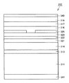
(実施例1)
図5に、実施例1の窒化物半導体レーザ素子110の好ましい一例の模式的な断面図を示す。実施例1の窒化物半導体レーザ素子110は、厚さ400μmで2インチのウエハのn型GaNからなる窒化物半導体基板111上に、厚さ2.5μmのn型Al0.05Ga0.95Nからなる第一クラッド層113、厚さ0.1μmのn型GaNからなる第一n型ガイド層114、厚さ0.2μmのp型GaNからなるp型ガイド層121、厚さ0.01μmのp型Al0.1Ga0.9Nからなるp型キャリアブロック層122、厚さ0.152μmのAlpInqGarN(0≦p≦1、0≦q≦1、0≦r≦1)からなる活性層123、厚さ0.2μmのn型GaNからなる第二n型ガイド層116および厚さ0.6μmのn型Al0.05Ga0.95Nからなる第二クラッド層117を、MOCVD成膜装置を用いてこの順に形成した。ここで、第二n型ガイド層116と第二クラッド層117とをあわせて第二n型窒化物半導体層115という。なお、第一クラッド層113から活性層123の窒化物半導体基板111に近い側のノンドープGaN層までを1125℃で成膜し、残りの層を850℃で成膜した。
Example 1
FIG. 5 shows a schematic cross-sectional view of a preferred example of the nitride
その後、リッジストライプ部170を形成するために、フォトリソグラフィ工程によって第二クラッド層117上にストライプ状のマスクを形成し、誘導結合プラズマ(ICP:Inductively Coupled Plasma)エッチング法を用いて、マスクが形成されていない部分を第二n型ガイド層116の途中までエッチングにより除去し、幅1.6μmのリッジストライプ部170を形成した。そして、厚さ200nmのSiO2と厚さ50nmのTiO2とからなる電流狭窄絶縁膜125をEB蒸着法により形成し、ストライプ状のマスクとマスク上の電流狭窄絶縁膜125をリフトオフ法により除去し、その後窒化物半導体基板111に接するように厚さ30nmのハフニウム層と厚さ200nmのアルミニウム層と厚さ30nmのモリブデン層と厚さ50nmの白金と厚さ200nmの金との5層からなる第一電極141を形成した。さらに、EB蒸着法によって第二電極140を形成した。
Thereafter, in order to form the
ここで、本実施例に用いられる活性層123は、厚さ60nmのノンドープGaN層、厚さ10nmのノンドープIn0.04Ga0.96Nからなるバリア層、厚さ4nmのノンドープIn0.25Ga0.75Nからなる井戸層、厚さ10nmのノンドープIn0.04Ga0.96Nからなるバリア層、厚さ4nmのノンドープIn0.25Ga0.75Nからなる井戸層および厚さ60nmのノンドープGaN層を窒化物半導体基板側からこの順に含むAlGaInN多重井戸活性層構造に作製したものであった。
Here, the
上記のようにして得られた、窒化物半導体ウエハの窒化物半導体基板111を研削、研磨工程して100μm程度に薄くして、ダイヤモンド針でスクライブし、バー状にへき開し、このへき開されて形成された端面に厚さ30nm程度のAlOxN1-x(0≦x≦1)からなる端面コート膜を形成し、この端面コート膜上にさらに酸化アルミニウム膜を反射率調整用に形成した。このような窒化物半導体レーザ素子の光出射側の端面の反射率は10%であり、光反射側の反射率は95%であった。このように実施例1のレーザは、端面光出射型の窒化物半導体レーザである。
The
このようにして作製した窒化物半導体レーザ素子の発振閾値と発振後の平均発光効率(スロープ効率)を求めたところ、実施例1の窒化物半導体レーザ素子20個の平均発振閾値は30mAであり、平均発光効率は1.65W/Aであった。ここで、発振閾値とは窒化物半導体レーザ素子の駆動電流の低さを表す値で、値が小さいほど駆動電流が小さい発光素子であることを示す。また、発光効率とは、窒化物半導体レーザ素子の電流注入量に対して素子外部に取り出すことができる光子の割合を表す値であって、値が大きいほど優れた発光素子であることを示す。 When the oscillation threshold value of the nitride semiconductor laser device thus fabricated and the average emission efficiency (slope efficiency) after oscillation were determined, the average oscillation threshold value of the 20 nitride semiconductor laser devices of Example 1 was 30 mA. The average luminous efficiency was 1.65 W / A. Here, the oscillation threshold is a value representing the low driving current of the nitride semiconductor laser device, and the smaller the value is, the light emitting device having a smaller driving current. The luminous efficiency is a value that represents the ratio of photons that can be extracted outside the element with respect to the current injection amount of the nitride semiconductor laser element, and the larger the value, the better the light emitting element.
また、比較のために特許文献1に示された窒化物半導体レーザ素子を同一の方法で作製し、上記と同様の方法で平均発振閾値と平均発光効率とを求めたところ、特許文献1の窒化物半導体レーザ素子20個の平均発振閾値は38mAであり、平均発光効率は1.35W/Aであった。以上のことから、実施例1で作製された窒化物半導体レーザ素子は特許文献1の窒化物半導体レーザ素子に比べ、平均発振閾値と平均発光効率の特性を大きく向上することができた。これは、実施例1においてはMgをドープしたp型AlGaNクラッドがなくなり、光吸収が抑制され内部ロス(αi)が低減したためと考えられる。
For comparison, the nitride semiconductor laser element disclosed in
(実施例2)
図6に本発明の実施例2で作製した窒化物半導体レーザ素子210の模式的な斜視図を示す。本実施例の窒化物半導体レーザ素子210は実施例1と類似の構造をしており、実施例1の窒化物半導体レーザ素子110における第一クラッド層113の一部と第一n型ガイド層114の全部とをp型クラッド層213aに置き代えている点と、第二クラッド層217と第二電極240との間に、n型コンタクト層218を設けた点とが異なっており、これらの点を特徴とする。また、実施例2の窒化物半導体レーザ素子210の活性層223の構造は実施例1のそれと同一の構造であるが、井戸層のIn組成を0.15とし、発振波長が450nmとなっている点で異なっている。
(Example 2)
FIG. 6 is a schematic perspective view of the nitride
実施例2の窒化物半導体レーザ素子210は、実施例1と同様のMOCVD装置によって、厚さ400μmのn型GaN基板からなる窒化物半導体基板211上に、厚さ2.3μmのn型Al0.05Ga0.95Nからなる第一クラッド層213、厚さ0.2μmのp型Al0.03Ga0.97Nからなるp型クラッド層213a、厚さ0.2μmのp型ガイド層221、厚さ0.01μmのp型キャリアブロック層222、厚さ0.152μmの活性層223、厚さ0.2μmの第二n型ガイド層216、厚さ0.6μmのn型Al0.05Ga0.95Nからなる第二クラッド層217および厚さ0.2μmのGaNからなるn型コンタクト層218をこの順に形成し、その後、実施例1と同様の方法によって、電流狭窄絶縁膜225、第一電極241および第二電極240を形成した。
The nitride
実施例2のように、第一クラッド層213の一部と第一n型ガイド層の全部とをp型クラッド層213aに代えることによっても、平均発振閾値と平均発光効率が良好であり、実施例1と同様の効果が得られた。
As in Example 2, the average oscillation threshold and the average luminous efficiency are good by replacing part of the
(実施例3)
図7に本発明の実施例3で作製した窒化物半導体レーザ素子310の模式的な斜視図を示す。本実施例の窒化物半導体レーザ素子310は、実施の形態2で示した窒化物半導体レーザ素子のように電流狭窄絶縁層を埋め込み式の形で備えている。また、実施例3の窒化物半導体レーザ素子310の活性層323の構造は実施例1のそれと同一の構造であるが、井戸層のIn組成を0.20としている点で異なっている。
(Example 3)
FIG. 7 is a schematic perspective view of the nitride
実施例3の窒化物半導体レーザ素子310の層構造は、図7に示されるように、厚さ400μmのn型GaNからなる窒化物半導体基板311上に、厚さ2.5μmのn型Al0.05Ga0.95Nからなる第一クラッド層313、厚さ0.1μmのn型GaNからなる第一n型ガイド層314、厚さ0.2μmのGaNからなるp型ガイド層321、厚さ0.01μmのAl0.1Ga0.9Nからなるp型キャリアブロック層322および厚さ0.152μmのAlxGa1-xInNからなる活性層323をMOCVD法により作製し、この窒化物半導体ウエハをMOCVD装置から取り出し、厚さ500nmのSiO2からなる電流狭窄絶縁膜325をスパッタ装置により成膜した。
As shown in FIG. 7, the layer structure of the nitride
その後、フォトリソプロセスによってSiO2上にレジストを塗り、幅2μm程度のストライプ状にレジストを加工し、誘導結合プラズマ(ICP:Inductively Coupled Plasma)による気相エッチングを行ない、SiO2をストライプ状に除去し、レジストを除去して、再びMOCVD装置に導入し、厚さ0.2μmのGaNからなる第二n型ガイド層316、厚さ0.6μmのn型Al0.05Ga0.95Nからなる第二クラッド層317、厚さ0.2μmのn型GaNからなるn型コンタクト層318を窒化物半導体基板311側からこの順にMOCVD法によって成膜し、さらに、第一電極341、第二電極340を形成した。
After that, a resist is applied onto SiO 2 by a photolithographic process, the resist is processed into a stripe shape having a width of about 2 μm, and gas phase etching by inductively coupled plasma (ICP) is performed to remove SiO 2 in a stripe shape. Then, the resist is removed and introduced into the MOCVD apparatus again, the second n-
実施例1で示された理由と同じ理由で、実施例3で作製された窒化物半導体レーザ素子310は、活性層323を成膜したあと、p型窒化物半導体層を1000℃以上の高温で成膜する必要がないため、活性層323の井戸層のIn組成xが0.15以上程度の高い組成を必要とする活性層を有する窒化物半導体レーザ素子も製造することができる。この実施例3で作製された窒化物半導体レーザ素子も従来例と比べ、平均発振閾値と平均発光効率が良好であり、実施例1と同様の効果が得られた。
For the same reason as described in the first embodiment, the nitride
(実施例4)
実施例4の窒化物半導体レーザ素子410の層構造は実施例3と類似の構造をしているが、実施例3の窒化物半導体レーザ素子における第二クラッド層およびn型コンタクト層の代わりにインジウムスズ酸化物(ITO:Indium Tin Oxide)からなる導電性酸化物層424を用いている点において異なり、この点を特徴としている。また、実施例4の窒化物半導体レーザ素子の活性層の構造は実施例1のそれと同一の構造であるが、井戸層のIn組成を0.27とし、発振波長は520nmとなっている点で異なっている。
Example 4
The layer structure of the nitride
実施例4の窒化物半導体レーザ素子410の層構造は、図8に示されるように、厚さ400μmのn型GaNからなる窒化物半導体基板411上に、厚さ2.5μmのn型Al0.05Ga0.95Nからなる第一クラッド層413、厚さ0.1μmのn型GaNからなる第一n型ガイド層414、厚さ0.2μmのGaNからなるp型ガイド層421、厚さ0.01μmのAl0.1Ga0.9Nからなるp型キャリアブロック層422および厚さ0.152μmのAlxGa1-xInNからなる活性層423までをMOCVD法により作製した後に、この窒化物半導体ウエハをMOCVD装置から取り出し、厚さ500nmのSiO2からなる電流狭窄絶縁膜425をスパッタ装置により成膜した。
As shown in FIG. 8, the layer structure of the nitride
その後、実施例3と同様の方法によってSiO2からなる電流狭窄絶縁膜425を形成した後に、再びMOCVD装置に導入し、厚さ0.2μmのGaNからなる第二n型ガイド層416をMOCVD法によって成膜し、厚さ0.3μmのインジウムスズ酸化物からなる導電性酸化物層424をスパッタ成膜法によって成膜し、最後に第一電極441、第二電極440を形成した。
Thereafter, a current
このように、第二クラッド層およびn型コンタクト層の代わりに導電性酸化物層424を用いることによって、活性層423上に第二クラッド層を形成する必要がなくなるため、さらに低抵抗化が可能となった。実施例4で作製された窒化物半導体レーザ素子も従来例と比べ、平均発振閾値と平均発光効率が良好であり、実施例1と同様の効果が得られた。
As described above, by using the
(実施例5)
本実施例では、電気伝導性のないサファイア基板上に実施例1で示した窒化物半導体基板を作製した。本実施例の窒化物半導体レーザ素子510は、サファイア基板から見て同一方向に第一電極541と第二電極540とが形成されており、第一n型窒化物半導体層上に第一電極541を設けていることを特徴とする。
(Example 5)
In this example, the nitride semiconductor substrate shown in Example 1 was fabricated on a sapphire substrate having no electrical conductivity. In the nitride
本実施例の窒化物半導体レーザ素子510は図9に示されるように、サファイア基板501上に、厚さ5μmのGaNからなるバッファ層502を成膜し、バッファ層502上にn型AlyGa1-yNからなる第一クラッド層513、n型GaNからなる第一n型ガイド層514、p型GaNからなるp型ガイド層521、p型AlyGa1-yNからなるp型キャリアブロック層522、AlpInqGarN(0≦p<1、0≦q<1、0≦r<1)からなる活性層523、n型GaNからなる第二n型ガイド層516およびn型AlyGa1-yNからなる第二クラッド層517を、MOCVD成膜装置を用いてこの順に形成し、その後、リッジストライプ部を形成するために、フォトリソグラフィ工程等によってマスクが形成されていない部分を第二n型ガイド層516の途中までエッチングにより除去し、リッジストライプ部を形成した。
As shown in FIG. 9, the nitride
そして、電流狭窄絶縁膜525をEB蒸着法により形成し、ストライプ状のマスクとマスク上の電流狭窄絶縁膜525をリフトオフ法により除去し、第二電極540を形成した。また、第一クラッド層513の途中まで上記で示したフォトリソグラフィ工程によりエッチングにより除去して、更に、エッチングにより露出した第一クラッド層513上に第一電極541を形成した。このように、第一n型窒化物半導体層上に第一電極541を設けることによっても、従来例と比べ、平均発振閾値と平均発光効率が良好であり、実施例1と同様の効果が得られた。なお、本実施例では基板にサファイア基板を用いているが、SiC、GaN、ZnO、Si等の基板を用いても同様の効果を得ることができる。
Then, the current
(実施例6)
図10に本発明の実施例6で作製した窒化物半導体レーザ素子の模式的な斜視図を示す。実施例6の窒化物半導体レーザ素子は、実施例1の窒化物半導体レーザ素子と類似の構造をしており、実施例1〜5は第一n型ガイド層および第二n型ガイド層の材料にGaNを用い、第一クラッド層および第二クラッド層の材料にInGaNを用いていたが、実施例6においては第一n型ガイド層および第二n型ガイド層の材料にInGaNを用い、第一クラッド層および第二クラッド層の材料にGaNを用いることを特徴としている。このように、第一n型ガイド層および第二n型ガイド層にInGaNを用い、第一クラッド層および第二クラッド層にGaNを用いることによっても、実施例1と同様の効果を得ることができる。また、実施例6の窒化物半導体レーザ素子の活性層の構造は実施例1のそれと同一の構造であるが、井戸層のIn組成を0.30とした。
(Example 6)
FIG. 10 is a schematic perspective view of the nitride semiconductor laser device manufactured in Example 6 of the present invention. The nitride semiconductor laser device of Example 6 has a similar structure to the nitride semiconductor laser device of Example 1, and Examples 1 to 5 are materials for the first n-type guide layer and the second n-type guide layer. GaN was used for the first clad layer and the second clad layer. In Example 6, InGaN was used for the first n-type guide layer and the second n-type guide layer. GaN is used as the material of the first cladding layer and the second cladding layer. Thus, the same effect as in Example 1 can be obtained by using InGaN for the first n-type guide layer and the second n-type guide layer and using GaN for the first cladding layer and the second cladding layer. it can. The structure of the active layer of the nitride semiconductor laser device of Example 6 is the same as that of Example 1, but the In composition of the well layer was set to 0.30.
実施例6の窒化物半導体レーザ素子610の層構造は、図10に示されるように、実施例1と同様のMOCVD装置によって、厚さ400μmのn型GaN基板からなる窒化物半導体基板611上に、厚さ4.5μmのn型GaNからなる第一クラッド層613、厚さ0.1μmのn型InGaNからなる第一n型ガイド層614、厚さ0.2μmのp型InGaNからなるp型ガイド層621、厚さ0.01μmのp型Al0.1Ga0.9Nからなるp型キャリアブロック層622、厚さ0.152μmのAlpInqGarN(0≦p≦1、0≦q≦1、0≦r≦1)からなる活性層623、厚さ0.2μmのn型InGaNからなる第二n型ガイド層616、厚さ1μmのn型GaNからなる第二クラッド層617および厚さ0.2μmのn型GaNからなるn型コンタクト層618をこの順に形成し、その後、実施例1と同様の方法によって、電流狭窄絶縁膜625、第一電極641および第二電極640を形成した。
As shown in FIG. 10, the layer structure of the nitride
このように第一クラッド層613および第二クラッド層617の材料にGaNを用い、第一n型ガイド層614および第二n型ガイド層616の材料にInGaNを用いる窒化物半導体レーザ素子であっても、従来例と比べ、平均発振閾値と平均発光効率が良好であり、実施例1と同様の効果が得られた。
Thus, a nitride semiconductor laser device using GaN as the material of the
(実施例7)
実施例1〜6によって製造された窒化物半導体レーザ素子はn型GaN基板の主面はc面{0001}を用いていたが、実施例7で作製した窒化物半導体レーザ素子は、n型GaN基板の主面にM面{1−100}の基板を用いることを特徴としている。また、実施例7の窒化物半導体レーザ素子の活性層の構造は実施例1のそれと同一の構造であるが、井戸層のIn組成を0.30とした。本実施例では、基板が主面に対してオフ角度を0.2°で作製したところ、面内の膜厚ばらつきは、50nm程度であり、従来例と比べ、平均発振閾値と平均発光効率が良好であり、実施例1と同様の効果が得られた。また、基板の主面に対するオフ角度は、0°より大きく2°以下の範囲であれば、面内の膜厚ばらつきが50nm程度と良好であった。
(Example 7)
The nitride semiconductor laser elements manufactured in Examples 1-6 used the c-plane {0001} as the main surface of the n-type GaN substrate, but the nitride semiconductor laser elements manufactured in Example 7 were n-type GaN. A feature is that a M-plane {1-100} substrate is used as the main surface of the substrate. Further, the structure of the active layer of the nitride semiconductor laser device of Example 7 is the same as that of Example 1, but the In composition of the well layer was set to 0.30. In this example, when the substrate was fabricated with an off angle of 0.2 ° with respect to the main surface, the in-plane film thickness variation was about 50 nm, and the average oscillation threshold and the average luminous efficiency were higher than in the conventional example. It was good and the same effect as Example 1 was acquired. In addition, when the off angle with respect to the main surface of the substrate is in the range of greater than 0 ° and less than or equal to 2 °, the in-plane film thickness variation was good at about 50 nm.
(実施例8)
図11に本発明の実施例8で作製した窒化物半導体レーザ素子の模式的な斜視図を示す。本実施例の窒化物半導体レーザ素子810の構造は実施例3の窒化物半導体レーザ素子の構造と類似しているが、n型GaN基板の主面にM面{1−100}を用いている点と、活性層823上に、n型Al0.12Ga0.88Nからなるn型キャリアブロック層816aが形成されている点とが実施例3と異なり、この点を本実施例の特徴としている。また、実施例8の窒化物半導体レーザ素子810の活性層823の構造は実施例1の構造と同一であるが、井戸層のIn組成を0.22としている点で異なっている。
(Example 8)
FIG. 11 is a schematic perspective view of the nitride semiconductor laser device manufactured in Example 8 of the present invention. The structure of the nitride
このように活性層823上にn型キャリアブロック層816aを作製することにより、キャリアの熱によるオーバーフローを低減でき、温度特性を改善できるだけでなく、活性層823上の面内平坦性が向上し、800℃程度の比較的低温で成膜を行ったときの結晶性が良くなるというメリットがある。
By forming the n-type
実施例8の窒化物半導体レーザ素子810の層構造は、図11に示されるように、厚さ400μmのn型GaNからなる窒化物半導体基板811上に、厚さ2.5μmのn型Al0.05Ga0.95Nからなる第一クラッド層813、厚さ0.1μmのn型GaNからなる第一n型ガイド層814、厚さ0.2μmのp型GaNからなるp型ガイド層821、厚さ0.01μmのp型Al0.1Ga0.9Nからなるp型キャリアブロック層822、厚さ0.152μmのAlxGa1-xInNからなる活性層823までをMOCVD法により作製した後に、このウエハをMOCVD装置から取り出し、厚さ500nmのSiO2からなる電流狭窄絶縁膜825をスパッタ装置により成膜した。その後、実施例3と同様の方法でSiO2をストライプ状に除去した。更に、レジストを除去して、再びMOCVD装置に導入し、厚さ0.2μmのn型Al0.12Ga0.88Nからなるn型キャリアブロック層816a、厚さ0.2μmのGaNからなる第二n型ガイド層816、厚さ0.6μmのn型Al0.05Ga0.95Nからなる第二クラッド層817および厚さ0.2μmのn型GaNからなるn型コンタクト層818を窒化物半導体基板811側からこの順にMOCVD法によって成膜し、さらに、第一電極840、第二電極841を形成した。
As shown in FIG. 11, the layer structure of the nitride
実施例8で作製した窒化物半導体レーザ素子も従来例と比べ、平均発振閾値と平均発光効率が良好であり、実施例1と同様の効果が得られた。 The nitride semiconductor laser device fabricated in Example 8 also had a better average oscillation threshold and average emission efficiency than the conventional example, and the same effects as in Example 1 were obtained.
(実施例9)
実施例9は実施例6の窒化物半導体レーザ素子においてn型コンタクト層の代わりに錫ドープ酸化インジウムからなる導電性酸化物層を用いることを特徴としている。なお、活性層は実施例6と同一のものを用いている。
Example 9
Example 9 is characterized in that a conductive oxide layer made of tin-doped indium oxide is used in place of the n-type contact layer in the nitride semiconductor laser element of Example 6. Note that the same active layer as in Example 6 is used.
すなわち、実施例6と同一の方法で第二クラッド層まで作製し、その後300℃程度の比較的低温で厚さ0.2μmの錫ドープ酸化インジウムからなる導電性酸化物層を形成した。導電性酸化物層を成膜することによって、実施例9の窒化物半導体発光素子を作製した。実施例9で作製した窒化物半導体レーザ素子も従来例と比べ、平均発振閾値と平均発光効率が良好であり、実施例1と同様の効果が得られた。 That is, the second clad layer was formed by the same method as in Example 6, and then a conductive oxide layer made of tin-doped indium oxide having a thickness of 0.2 μm was formed at a relatively low temperature of about 300 ° C. A nitride semiconductor light emitting device of Example 9 was fabricated by forming a conductive oxide layer. The nitride semiconductor laser element fabricated in Example 9 also had a better average oscillation threshold and average emission efficiency than the conventional example, and the same effects as in Example 1 were obtained.
(実施例10)
実施例10の窒化物半導体レーザ素子の層構造は実施例8と類似の構造をしているが、第一n型ガイド層とp型ガイド層との間にp+GaN層およびn+GaN層を設けている点において異なり、この点を特徴としている。
(Example 10)
The layered structure of the nitride semiconductor laser device of Example 10 is similar to that of Example 8, except that a p + GaN layer and an n + GaN layer are provided between the first n-type guide layer and the p-type guide layer. It is different in point and is characterized by this point.
このように、第一n型ガイド層とp型ガイド層との間にp+GaN層およびn+GaN層を設けることによって、第一n型ガイド層とp型ガイド層との間の空乏層が狭くなり、もってpn接合の抵抗値が小さくなりトンネル電流が流れやすくなるというメリットがある。このように実施例10で作製された窒化物半導体レーザ素子も従来例と比べ、平均発振閾値と平均発光効率が良好であり、実施例1と同様の効果が得られた。 Thus, by providing the p + GaN layer and the n + GaN layer between the first n-type guide layer and the p-type guide layer, the depletion layer between the first n-type guide layer and the p-type guide layer becomes narrower, Therefore, there is an advantage that the resistance value of the pn junction is reduced and the tunnel current easily flows. Thus, the nitride semiconductor laser device fabricated in Example 10 also had a better average oscillation threshold and average emission efficiency than the conventional example, and the same effects as in Example 1 were obtained.
(実施例11)
実施例11の窒化物半導体レーザ素子の層構造は実施例8と類似の構造をしているが、第一n型ガイド層とp型ガイド層との間にAlyGa1-yN中間層を設けている点において異なり、この点を特徴としている。
(Example 11)
The layer structure of the nitride semiconductor laser device of Example 11 is similar to that of Example 8, but the Al y Ga 1-y N intermediate layer is interposed between the first n-type guide layer and the p-type guide layer. It is different in that it is provided with this feature.
このように、第一n型ガイド層とp型ガイド層との間にAlyGa1-yN中間層を設けることによって、空乏層の幅が小さくなりトンネル電流が流れやすくなるというメリットがある。 Thus, by providing the Al y Ga 1-y N intermediate layer between the first n-type guide layer and the p-type guide layer, there is an advantage that the width of the depletion layer is reduced and the tunnel current can easily flow. .
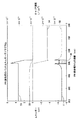
本実施例のpn接合付近のバンドエネルギーダイヤグラムを図12に示す。図12において、横軸はPN接合部からの距離を表しており、横軸の500の位置がAlyGa1-yN中間層とp型ガイド層との界面であり、2.5nmのAlyGa1-yN中間層が形成された場合を示している。なお、横軸の単位はnmである。左側の縦軸は、エネルギー(eV)を表しており、右側の縦軸はキャリア濃度(/cm3)の分布を表している。また、p型ガイド層からpn接合までのp型キャリア密度51の分布を表す曲線と、第一n型ガイド層からpn接合までのn型キャリア密度52の分布を表す曲線とから、窒化物半導体レーザ素子の空乏層の幅60を求めることができ、この空乏層の幅60が大きくなるほど、トンネル電流が流れにくいことを示している。
FIG. 12 shows a band energy diagram near the pn junction of this example. In FIG. 12, the horizontal axis represents the distance from the PN junction, and the
また、本実施例の窒化物半導体レーザ素子のpn接合付近のバンドエネルギーダイヤグラムにおいて、伝導帯バンドエネルギー53の変移と、価電子帯バンドエネルギー54の変移とが図12のように表され、このフェルミエネルギー55が一致した平衡状態を示している。この実施例11の窒化物半導体レーザ素子の空乏層の幅は、2.5nmとなり、これは実施例10の窒化物半導体レーザ素子の空乏層の幅の10分の1程度の幅となっていることがわかった。以上のことから、第一n型ガイド層とp型ガイド層との間にAlyGa1-yN中間層を設けることによって、空乏層の幅が大幅に狭くなり、素子を低抵抗化することができ、もって、トンネル電流が流れやすくなることがわかった。
Further, in the band energy diagram in the vicinity of the pn junction of the nitride semiconductor laser device of this example, the transition of the
このように実施例11で作製された窒化物半導体レーザ素子も従来例と比べ、平均発振閾値と平均発光効率が良好であり、実施例1と同様の効果が得られた。 Thus, the nitride semiconductor laser device fabricated in Example 11 also had better average oscillation threshold and average emission efficiency than the conventional example, and the same effects as in Example 1 were obtained.
(実施例12)
本実施例の窒化物半導体レーザ素子は、実施例1の窒化物半導体レーザの構造と同じであるが、基板にGaAs基板を用いたGaAs系半導体レーザであることを特徴とする。すなわち、GaAs基板上に厚さ0.5μmのn型GaAsバッファ層、厚さ2.0μmのIn0.49(Ga0.3Al0.7)0.51Pからなる第一クラッド層、厚さ50nmの(Al0.50Ga0.50)InPからなるp型ガイド層、GaInPからなる井戸層(4層、厚さ6nm)と(Al0.50Ga0.50)InPからなるバリア層(3層、厚さ5nm)とからなる活性層、厚さ50nmの(Al0.50Ga0.50)InPからなるn型ガイド層、n型のIn0.49(Ga0.3Al0.7)0.51Pからなる第二クラッド層、厚さ0.4μmのn型GaAsコンタクト層を形成した。
Example 12
The nitride semiconductor laser device of the present embodiment has the same structure as that of the nitride semiconductor laser of
その後に上述したような一般的なプロセスを用いて、InGaAlPからなるn型ガイド層までエッチングにより除去し、リッジストライプ形状の端面出射型のGaAs系赤色半導体レーザを作製した。リッジストライプ部の両脇には、電流狭窄絶縁膜が形成されている。p型のドーパント材料として、MgもしくはZn、Beが用いられる。このように、GaAs系半導体レーザにおいても好適に用いられる。また、n型ZnO、p型ZnOを用いた、若しくはGaNとZnOを組み合わせることで作製された半導体レーザを用いてもよい。 Thereafter, the n-type guide layer made of InGaAlP was removed by etching using a general process as described above, and a ridge-stripe edge-emitting GaAs red semiconductor laser was fabricated. A current confinement insulating film is formed on both sides of the ridge stripe portion. Mg, Zn, or Be is used as the p-type dopant material. Thus, it can be suitably used also in a GaAs semiconductor laser. A semiconductor laser using n-type ZnO, p-type ZnO, or a combination of GaN and ZnO may be used.
(実施例13)
本実施例の窒化物半導体レーザ素子の構造は、実施例4の窒化物半導体レーザ素子と活性層まで構造が同じで、活性層を成膜した後活性層上にキャリアブロック層が形成されていることを特徴とする。以下に実施例13の窒化物半導体レーザ素子の製造方法について説明する。
(Example 13)
The structure of the nitride semiconductor laser device of this example is the same as that of the nitride semiconductor laser device of Example 4 up to the active layer, and after forming the active layer, a carrier block layer is formed on the active layer. It is characterized by that. A method for manufacturing the nitride semiconductor laser element of Example 13 will be described below.
実施例4と同様の方法で活性層までを成膜した後、厚さ20nmのn型Al0.12Ga0.88Nからなるキャリアブロック層を形成し、その後、窒化物半導体ウエハをMOCVD装置から取り出し、厚さ500nmのSiO2からなる電流狭窄絶縁膜をスパッタ装置により成膜した。その後、実施例4と同様の方法によってSiO2からなる電流狭窄絶縁膜を形成した後に、再びMOCVD装置に導入し、キャリアブロック層上に厚さ0.2μmのn型ZnOからなる第二n型ガイド層を形成した。その後、厚さ0.3μmのインジウムスズ酸化物からなる導電性酸化物層をスパッタ成膜法によって成膜し、最後に第一電極、第二電極を形成した。 After forming up to the active layer by the same method as in Example 4, a carrier block layer made of n-type Al 0.12 Ga 0.88 N having a thickness of 20 nm is formed. Thereafter, the nitride semiconductor wafer is taken out from the MOCVD apparatus, and the thickness is increased. A current confinement insulating film made of SiO 2 having a thickness of 500 nm was formed by a sputtering apparatus. Thereafter, a current confinement insulating film made of SiO 2 is formed by the same method as in Example 4, and then introduced again into the MOCVD apparatus, and the second n-type made of n-type ZnO having a thickness of 0.2 μm is formed on the carrier block layer. A guide layer was formed. Thereafter, a conductive oxide layer made of indium tin oxide having a thickness of 0.3 μm was formed by sputtering, and finally a first electrode and a second electrode were formed.
本実施例のように、窒化物半導体層上にn型ZnOを、スパッタ法、MBE法、MOCVD法、PLD法等で形成しても、従来例と比べ、平均発振閾値と平均発光効率が良好であり、実施例1と同様の効果が得られた。 Even if n-type ZnO is formed on the nitride semiconductor layer by sputtering, MBE, MOCVD, PLD, etc. as in this embodiment, the average oscillation threshold and the average luminous efficiency are better than the conventional examples. Thus, the same effect as in Example 1 was obtained.
(比較例1)
比較例1の窒化物半導体レーザ素子は、実施例7で作製した窒化物半導体レーザ素子は、n型GaN基板の主面がM面{1−100}の基板を用い、基板が主面に対してオフ角度を0°で作製したところ、実施例7の窒化物系半導体レーザ素子は面内の膜厚ばらつきは50nm程度であったが、比較例1の窒化物系半導体レーザ素子の面内の膜厚ばらつきは、200〜300nm程度であり、実施例1と同様の効果は得られなかった。
(Comparative Example 1)
The nitride semiconductor laser element of Comparative Example 1 is the same as that of the nitride semiconductor laser element manufactured in Example 7, except that the main surface of the n-type GaN substrate is an M-plane {1-100} substrate. When the off-angle was manufactured at 0 °, the nitride semiconductor laser element of Example 7 had an in-plane film thickness variation of about 50 nm, but the nitride semiconductor laser element of Comparative Example 1 had an in-plane thickness variation of about 50 nm. The film thickness variation was about 200 to 300 nm, and the same effect as in Example 1 was not obtained.
なお、本明細書中で窒化物半導体レーザ素子と表現しているが、この窒化物半導体レーザ素子は半導体レーザに用いられる素子のみに限られず、発光ダイオードに用いられる窒化物半導体発光ダイオード素子も含まれる。 In addition, although expressed as a nitride semiconductor laser element in this specification, this nitride semiconductor laser element is not limited to an element used for a semiconductor laser, but also includes a nitride semiconductor light emitting diode element used for a light emitting diode. It is.
今回開示された実施の形態および実施例はすべての点で例示であって制限的なものではないと考えられるべきである。本発明の範囲は上記した説明ではなくて特許請求の範囲によって示され、特許請求の範囲と均等の意味および範囲内でのすべての変更が含まれることが意図される。 It should be understood that the embodiments and examples disclosed herein are illustrative and non-restrictive in every respect. The scope of the present invention is defined by the terms of the claims, rather than the description above, and is intended to include any modifications within the scope and meaning equivalent to the terms of the claims.
本発明によれば、より低出力で駆動でき、かつ発光効率のより高く、しかも440〜550nm程度の長波長の光を発光する窒化物半導体レーザ素子を提供することができる。 According to the present invention, it is possible to provide a nitride semiconductor laser device that can be driven at a lower output, has higher luminous efficiency, and emits light having a long wavelength of about 440 to 550 nm.
10,110,210,310,410,510,610,810,910,1010,2010 窒化物半導体レーザ素子、11 基板、501 サファイア基板、502 バッファ層、111,211,311,411,611,811,1011,2011 窒化物半導体基板、12 第一n型窒化物半導体層、13,113,213,313,413,513,613,813,1013,2013 第一クラッド層、14,114,314,414,514,614,814,1014,2014 第一n型ガイド層、14a n+ドープ層、15,115 第二n型窒化物半導体層、16,116,216,316,416,516,616,816,1016,2016 第二n型ガイド層、17,117,217,317,517,617,817,1017,2017 第二クラッド層、18,218,318,618,818,2018 n型コンタクト層、20 p型窒化物半導体層、21,121,221,321,421,521,621,821,1021,2021 p型ガイド層、21a p+ドープ層、22,122,222,322,422,522,622,822,1022,2022 p型キャリアブロック層、23,123,223,323,423,523,623,823,1023,2023 活性層、424 導電性酸化物層、25,125,225,325,425,525,625,825,1025,2025 電流狭窄絶縁膜、30 AlyGa1-yN中間層、40,140,240,340,440,540,640,840,1040,2040 第二電極、41,141,241,341,441,541,641,841,1041,2041 第一電極、51 p型キャリア密度、52 n型キャリア密度、53 伝導帯バンドエネルギー、54 価電子帯バンドエネルギー、55 フェルミエネルギー、60 空乏層の幅、70,170,1070 リッジストライプ部、213a p型クラッド層、816a n型キャリアブロック層、911 n型GaN基板、913 n型Al0.05Ga0.95Nクラッド層、914 n型GaNガイド層、920 p型窒化物半導体層、921 p型GaNガイド層、922 p型Al0.15Ga0.85Nキャリアブロック層、923 InGaN多重量子井戸活性層、924 p型Al0.05Ga0.95Nクラッド層、924a p型GaNコンタクト層、925 SiO2膜、940 p電極、941 n電極。 10, 110, 210, 310, 410, 510, 610, 810, 910, 1010, 2010 Nitride semiconductor laser element, 11 substrate, 501 sapphire substrate, 502 buffer layer, 111, 211, 311, 411, 611, 811 1011, 1011 nitride semiconductor substrate, 12 first n-type nitride semiconductor layer, 13, 113, 213, 313, 413, 513, 613, 813, 1013, 2013 first cladding layer, 14, 114, 314, 414 514, 614, 814, 1014, 2014 1st n-type guide layer, 14a n + doped layer, 15, 115 2nd n-type nitride semiconductor layer, 16, 116, 216, 316, 416, 516, 616, 816, 1016 , 2016 second n-type guide layer, 17, 117, 217, 317, 517, 617 817, 1017, 2017 Second clad layer, 18, 218, 318, 618, 818, 2018 n-type contact layer, 20 p-type nitride semiconductor layer, 21, 121, 221, 321, 421, 521, 621, 821, 1021, 2021 p-type guide layer, 21a p + doped layer, 22, 122, 222, 322, 422, 522, 622, 822, 1022, 2022 p-type carrier block layer, 23, 123, 223, 323, 423, 523 623,823,1023,2023 active layer, 424 a conductive oxide layer, 25,125,225,325,425,525,625,825,1025,2025 current narrowing insulating film, 30 Al y Ga 1-y N intermediate Layer, 40, 140, 240, 340, 440, 540, 640, 840, 1040, 204 0 second electrode, 41, 141, 241, 341, 441, 541, 641, 841, 1041, 2041 first electrode, 51 p-type carrier density, 52 n-type carrier density, 53 conduction band energy, 54 valence band Band energy, 55 Fermi energy, 60 depletion layer width, 70, 170, 1070 ridge stripe, 213a p-type cladding layer, 816a n-type carrier block layer, 911 n-type GaN substrate, 913 n-type Al 0.05 Ga 0.95 N cladding Layer, 914 n-type GaN guide layer, 920 p-type nitride semiconductor layer, 921 p-type GaN guide layer, 922 p-type Al 0.15 Ga 0.85 N carrier block layer, 923 InGaN multiple quantum well active layer, 924 p-type Al 0.05 Ga 0.95 N clad layer, 924a p-type GaN contact layer, 925 SiO 2 , 940 p electrode, 941 n electrode.
Claims (5)
前記第二n型窒化物半導体層は、第二電極と接し、
前記第一電極は、アノード電極であり、
前記第二電極は、カソード電極である、請求項1に記載の窒化物半導体レーザ素子。 The substrate or the first n-type nitride semiconductor layer is in contact with the first electrode;
The second n-type nitride semiconductor layer is in contact with the second electrode;
The first electrode is an anode electrode;
The nitride semiconductor laser element according to claim 1, wherein the second electrode is a cathode electrode.
前記導電性酸化物層は、第二電極と接し、
前記第一電極は、アノード電極であり、
前記第二電極は、カソード電極である、請求項3に記載の窒化物半導体レーザ素子。 The substrate or the first n-type nitride semiconductor layer is in contact with the first electrode;
The conductive oxide layer is in contact with the second electrode;
The first electrode is an anode electrode;
The nitride semiconductor laser element according to claim 3, wherein the second electrode is a cathode electrode.
前記井戸層のIn組成xは、0.15以上0.30以下である、請求項1〜4に記載の窒化物半導体レーザ素子。 The active layer includes a well layer made of In x Ga 1-x N;
The nitride semiconductor laser element according to claim 1, wherein an In composition x of the well layer is 0.15 or more and 0.30 or less.
Priority Applications (1)
| Application Number | Priority Date | Filing Date | Title |
|---|---|---|---|
| JP2008176167A JP2010016261A (en) | 2008-07-04 | 2008-07-04 | Nitride semiconductor laser element |
Applications Claiming Priority (1)
| Application Number | Priority Date | Filing Date | Title |
|---|---|---|---|
| JP2008176167A JP2010016261A (en) | 2008-07-04 | 2008-07-04 | Nitride semiconductor laser element |
Publications (2)
| Publication Number | Publication Date |
|---|---|
| JP2010016261A true JP2010016261A (en) | 2010-01-21 |
| JP2010016261A5 JP2010016261A5 (en) | 2011-01-20 |
Family
ID=41702070
Family Applications (1)
| Application Number | Title | Priority Date | Filing Date |
|---|---|---|---|
| JP2008176167A Pending JP2010016261A (en) | 2008-07-04 | 2008-07-04 | Nitride semiconductor laser element |
Country Status (1)
| Country | Link |
|---|---|
| JP (1) | JP2010016261A (en) |
Cited By (6)
| Publication number | Priority date | Publication date | Assignee | Title |
|---|---|---|---|---|
| JP2010080960A (en) * | 2008-09-24 | 2010-04-08 | Palo Alto Research Center Inc | Semiconductor light emitting device |
| WO2011105136A1 (en) * | 2010-02-25 | 2011-09-01 | 三洋電機株式会社 | Semiconductor laser device and optical device |
| WO2012127778A1 (en) * | 2011-03-24 | 2012-09-27 | パナソニック株式会社 | Nitride semiconductor light-emitting element |
| EP2369697A3 (en) * | 2010-03-25 | 2013-03-13 | Nichia Corporation | Semiconductor laser element and method of manufacturing thereof |
| JP2019201185A (en) * | 2018-05-18 | 2019-11-21 | 旭化成株式会社 | Laser diode |
| JP2020129653A (en) * | 2019-02-08 | 2020-08-27 | シャープ株式会社 | Light emitting device and manufacturing method thereof |
Citations (4)
| Publication number | Priority date | Publication date | Assignee | Title |
|---|---|---|---|---|
| JP2002319703A (en) * | 2001-04-20 | 2002-10-31 | Ricoh Co Ltd | Semiconductor device and its manufacturing method |
| JP2004128502A (en) * | 2002-09-30 | 2004-04-22 | Lumileds Lighting Us Llc | Light emitting device including tunnel junction |
| JP2004289157A (en) * | 2003-03-20 | 2004-10-14 | Xerox Corp | Laser diode structure and manufacturing method thereof |
| JP2006041491A (en) * | 2004-06-21 | 2006-02-09 | Matsushita Electric Ind Co Ltd | Semiconductor laser device and its manufacture |
-
2008
- 2008-07-04 JP JP2008176167A patent/JP2010016261A/en active Pending
Patent Citations (4)
| Publication number | Priority date | Publication date | Assignee | Title |
|---|---|---|---|---|
| JP2002319703A (en) * | 2001-04-20 | 2002-10-31 | Ricoh Co Ltd | Semiconductor device and its manufacturing method |
| JP2004128502A (en) * | 2002-09-30 | 2004-04-22 | Lumileds Lighting Us Llc | Light emitting device including tunnel junction |
| JP2004289157A (en) * | 2003-03-20 | 2004-10-14 | Xerox Corp | Laser diode structure and manufacturing method thereof |
| JP2006041491A (en) * | 2004-06-21 | 2006-02-09 | Matsushita Electric Ind Co Ltd | Semiconductor laser device and its manufacture |
Cited By (13)
| Publication number | Priority date | Publication date | Assignee | Title |
|---|---|---|---|---|
| JP2010080960A (en) * | 2008-09-24 | 2010-04-08 | Palo Alto Research Center Inc | Semiconductor light emitting device |
| JP2015099944A (en) * | 2008-09-24 | 2015-05-28 | パロ・アルト・リサーチ・センター・インコーポレーテッドPalo Alto Research Center Incorporated | Semiconductor light-emitting device |
| WO2011105136A1 (en) * | 2010-02-25 | 2011-09-01 | 三洋電機株式会社 | Semiconductor laser device and optical device |
| EP2369697A3 (en) * | 2010-03-25 | 2013-03-13 | Nichia Corporation | Semiconductor laser element and method of manufacturing thereof |
| US8942269B2 (en) | 2011-03-24 | 2015-01-27 | Panasonic Corporation | Nitride semiconductor light-emitting device |
| JPWO2012127778A1 (en) * | 2011-03-24 | 2014-07-24 | パナソニック株式会社 | Nitride semiconductor light emitting device |
| CN103444021A (en) * | 2011-03-24 | 2013-12-11 | 松下电器产业株式会社 | Nitride semiconductor light-emitting element |
| WO2012127778A1 (en) * | 2011-03-24 | 2012-09-27 | パナソニック株式会社 | Nitride semiconductor light-emitting element |
| CN103444021B (en) * | 2011-03-24 | 2016-04-27 | 松下知识产权经营株式会社 | Nitride semiconductor luminescent element |
| JP5963004B2 (en) * | 2011-03-24 | 2016-08-03 | パナソニックIpマネジメント株式会社 | Nitride semiconductor light emitting device |
| JP2019201185A (en) * | 2018-05-18 | 2019-11-21 | 旭化成株式会社 | Laser diode |
| JP7185867B2 (en) | 2018-05-18 | 2022-12-08 | 旭化成株式会社 | laser diode |
| JP2020129653A (en) * | 2019-02-08 | 2020-08-27 | シャープ株式会社 | Light emitting device and manufacturing method thereof |
Similar Documents
| Publication | Publication Date | Title |
|---|---|---|
| EP1453160B1 (en) | Semiconductor element | |
| US6724013B2 (en) | Edge-emitting nitride-based laser diode with p-n tunnel junction current injection | |
| US20100195687A1 (en) | Semiconductor laser device | |
| JP2008109066A (en) | Light emitting element | |
| WO2002080320A1 (en) | Nitride semiconductor element | |
| JP2008311640A (en) | Semiconductor laser diode | |
| US20110042646A1 (en) | Nitride semiconductor wafer, nitride semiconductor chip, method of manufacture thereof, and semiconductor device | |
| JP2008198952A (en) | Group iii nitride semiconductor light emitting device | |
| US8358674B2 (en) | Semiconductor laser element and method of manufacturing thereof | |
| JP2009094360A (en) | Semiconductor laser diode | |
| JP5444609B2 (en) | Semiconductor laser element | |
| JP3446660B2 (en) | Nitride semiconductor light emitting device | |
| JP2010016261A (en) | Nitride semiconductor laser element | |
| JP4291960B2 (en) | Nitride semiconductor device | |
| JP2001068786A (en) | Nitride compound semiconductor light-emitting device and its manufacture | |
| US20130105762A1 (en) | Nitride semiconductor light emitting device, method of fabricating nitride semiconductor light emitting device | |
| JP4877294B2 (en) | Manufacturing method of semiconductor light emitting device | |
| JP2003086903A (en) | Semiconductor light emitting device and its manufacturing method | |
| JP2008226865A (en) | Semiconductor laser diode | |
| JP2011119374A (en) | Nitride semiconductor element and method of manufacturing the same, and semiconductor device | |
| JP2011138891A (en) | Nitride semiconductor element | |
| JP5223531B2 (en) | Semiconductor laser element | |
| JP2000077783A (en) | Growth method of indium-containing nitride semiconductor crystal | |
| JP2008066550A (en) | Semiconductor light emitting device and manufacturing method of semiconductor light emitting device | |
| JP4628651B2 (en) | Manufacturing method of nitride semiconductor light emitting device |
Legal Events
| Date | Code | Title | Description |
|---|---|---|---|
| A521 | Written amendment |
Free format text: JAPANESE INTERMEDIATE CODE: A523 Effective date: 20101125 |
|
| A621 | Written request for application examination |
Free format text: JAPANESE INTERMEDIATE CODE: A621 Effective date: 20101125 |
|
| A977 | Report on retrieval |
Free format text: JAPANESE INTERMEDIATE CODE: A971007 Effective date: 20120120 |
|
| A131 | Notification of reasons for refusal |
Free format text: JAPANESE INTERMEDIATE CODE: A131 Effective date: 20120131 |
|
| A521 | Written amendment |
Free format text: JAPANESE INTERMEDIATE CODE: A523 Effective date: 20120328 |
|
| A02 | Decision of refusal |
Free format text: JAPANESE INTERMEDIATE CODE: A02 Effective date: 20120807 |