JP2010015663A - 相変化デバイスを用いた高密度コンテンツ・アドレス可能メモリ - Google Patents
相変化デバイスを用いた高密度コンテンツ・アドレス可能メモリ Download PDFInfo
- Publication number
- JP2010015663A JP2010015663A JP2008270695A JP2008270695A JP2010015663A JP 2010015663 A JP2010015663 A JP 2010015663A JP 2008270695 A JP2008270695 A JP 2008270695A JP 2008270695 A JP2008270695 A JP 2008270695A JP 2010015663 A JP2010015663 A JP 2010015663A
- Authority
- JP
- Japan
- Prior art keywords
- memory
- search
- resistance
- access device
- word
- Prior art date
- Legal status (The legal status is an assumption and is not a legal conclusion. Google has not performed a legal analysis and makes no representation as to the accuracy of the status listed.)
- Granted
Links
Images


Classifications
-
- G—PHYSICS
- G11—INFORMATION STORAGE
- G11C—STATIC STORES
- G11C15/00—Digital stores in which information comprising one or more characteristic parts is written into the store and in which information is read-out by searching for one or more of these characteristic parts, i.e. associative or content-addressed stores
- G11C15/02—Digital stores in which information comprising one or more characteristic parts is written into the store and in which information is read-out by searching for one or more of these characteristic parts, i.e. associative or content-addressed stores using magnetic elements
-
- G—PHYSICS
- G11—INFORMATION STORAGE
- G11C—STATIC STORES
- G11C11/00—Digital stores characterised by the use of particular electric or magnetic storage elements; Storage elements therefor
- G11C11/02—Digital stores characterised by the use of particular electric or magnetic storage elements; Storage elements therefor using magnetic elements
- G11C11/16—Digital stores characterised by the use of particular electric or magnetic storage elements; Storage elements therefor using magnetic elements using elements in which the storage effect is based on magnetic spin effect
-
- G—PHYSICS
- G11—INFORMATION STORAGE
- G11C—STATIC STORES
- G11C15/00—Digital stores in which information comprising one or more characteristic parts is written into the store and in which information is read-out by searching for one or more of these characteristic parts, i.e. associative or content-addressed stores
- G11C15/04—Digital stores in which information comprising one or more characteristic parts is written into the store and in which information is read-out by searching for one or more of these characteristic parts, i.e. associative or content-addressed stores using semiconductor elements
- G11C15/046—Digital stores in which information comprising one or more characteristic parts is written into the store and in which information is read-out by searching for one or more of these characteristic parts, i.e. associative or content-addressed stores using semiconductor elements using non-volatile storage elements
-
- G—PHYSICS
- G11—INFORMATION STORAGE
- G11C—STATIC STORES
- G11C13/00—Digital stores characterised by the use of storage elements not covered by groups G11C11/00, G11C23/00, or G11C25/00
- G11C13/0002—Digital stores characterised by the use of storage elements not covered by groups G11C11/00, G11C23/00, or G11C25/00 using resistive RAM [RRAM] elements
- G11C13/0004—Digital stores characterised by the use of storage elements not covered by groups G11C11/00, G11C23/00, or G11C25/00 using resistive RAM [RRAM] elements comprising amorphous/crystalline phase transition cells
Landscapes
- Engineering & Computer Science (AREA)
- Computer Hardware Design (AREA)
- Semiconductor Memories (AREA)
- Read Only Memory (AREA)
- Digital Transmission Methods That Use Modulated Carrier Waves (AREA)
Abstract
【解決手段】 ストアド・ワードをメモリ素子にストアするコンテンツ・アドレス可能メモリ・アレイを提供する。各メモリ素子は、少なくとも2つの相補的バイナリ・ビットのうちの1つを、少なくとも2つの相補的抵抗のうちの1つとしてストアする。各メモリ素子はアクセス・デバイスに電気的に結合される。コンテンツ・アドレス可能メモリ・アレイの一態様は、バイアス回路を用いて検索動作中にアクセス・デバイスにバイアスをかけることである。検索動作中、ビット・ストリングを含む検索ワードが受信される。各アクセス・デバイスはバイアスをかけられて、検索ワード内の対応する検索ビットの相補的な抵抗値になる。メモリ素子内にストアされたビットがアクセス・デバイス内の抵抗により表されるビットに対して相補的である場合に、検索ワードとストアド・ワードの間のマッチが指示される。
【選択図】 図4
Description
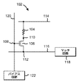
104、104a、104b、104c、104d:メモリ素子
106、106a、106b、106c、106d:アクセス・デバイス(アクセス・トランジスタ)
108:共通端子
110:第1端子
112:第2端子
114、406、406a、406b:ビットライン
116、408、408a、408b:マッチライン
118:マッチ回路
120、404、404a、404b:サーチライン
122:バイアス回路
202:マッチ抵抗の表
204:アクセス・トランジスタの抵抗
206:メモリ素子の抵抗
208:マッチラインの値
302:メモリ・アレイ
304:受信ユニット
306:バイアス・ユニット
308:マッチ・ユニット
310:中央処理装置(CPU)
312:メモリ・デバイス
402:コンテンツ・アドレス可能メモリ・アレイ
Claims (22)
- コンテンツ・アドレス可能メモリ・アレイを操作する方法であって、
前記コンテンツ・アドレス可能メモリ・アレイは、情報のビットの集合をストアド・ワードとしてストアするように配列された複数のメモリ・セルを含み、
各々の前記メモリ・セルは、直列回路内のアクセス・デバイスに電気的に結合されたメモリ素子を含み、
前記メモリ素子は、少なくとも2つの相補的抵抗のうちの1つとしてバイナリ・データをストアするように構成されていて、
前記コンテンツ・アドレス可能メモリ・アレイを通して検索する検索ワードを受信するステップと、
各ストアド・ワードの各メモリ・セルの前記アクセス・デバイスにバイアスをかけて、前記アクセス・デバイスの実効抵抗を前記検索ワードの対応するビットの相補的抵抗にする、バイアスをかけるステップと、
各ストアド・ワードの前記メモリ・セルの集合抵抗を計測するステップと、
前記集合抵抗が所定の値の範囲にある場合に、各ストアド・ワードに対して検索マッチを指示するステップとを含む
方法。 - 前記メモリ素子は、相変化素子、抵抗メモリ素子、浮遊ゲートFET、磁気抵抗ランダム・アクセス・メモリ(MRAM)、及び電荷トラップ・デバイスのうちの1つを含む、請求項1に記載の方法。
- 前記集合抵抗が所定の値の範囲内にある場合に、少なくとも1つのストアド・ワードのメモリ位置を指示するステップをさらに含む、請求項1に記載の方法。
- 前記アクセス・デバイスは金属酸化物半導体電界効果トランジスタ(MOSFET)である、請求項1に記載の方法。
- 前記アクセス・デバイスは、複数の前記アクセス・デバイスが単一のサーチライン導電体に電気的に結合されるように、サーチラインに電気的に結合される、請求項1に記載の方法。
- 前記コンテンツ・アドレス可能メモリ・アレイ内に記憶するストア・ワードを受信するステップであって、前記ストア・ワードの各々のビットが個々のメモリ・セルにストアされる、前記受信するステップと、
前記サーチライン内に所定の信号を加え、その結果、前記ストア・ワードを記憶するために用いられる所望のメモリ・セルの前記アクセス・デバイスを通過する電流パルスが前記メモリ素子を所望の抵抗値にプログラムすることにより、前記ストア・ワードを前記コンテンツ・アドレス可能メモリ・アレイ内にストアするステップと
をさらに含む、請求項5に記載の方法。 - 前記電気的に結合されたアクセス・デバイス及びメモリ素子は、複数の前記電気的に結合されたアクセス・デバイス及びメモリ素子が単一のビットライン及び単一のマッチラインに電気的に結合されるように、ビットライン及びマッチラインに電気的に結合される、請求項1に記載の方法。
- コンテンツ・アドレス可能メモリ・アレイであって、
ストアド・ワードをストアするように組み合された複数のメモリ・セルであって、該メモリ・セルの各々は直列回路内のアクセス・デバイスに電気的に結合されたメモリ素子を含み、該メモリ素子は少なくとも2つの相補的抵抗のうちの1つとしてバイナリ・データをストアするように構成される、複数のメモリ・セルと、
前記コンテンツ・アドレス可能メモリ・アレイを通して検索する検索ワードを受信するように構成された、受信ユニットと、
前記各メモリ・セルの前記アクセス・デバイスにバイアスをかけて、前記アクセス・デバイスの実効抵抗を前記検索ワードの対応するビットの相補的抵抗にするように構成された、バイアス・ユニットと、
前記ストアド・ワードの各々に関する前記メモリ・セルの集合抵抗を計測し、前記集合抵抗が所定の値の範囲内にある場合に、前記各ストアド・ワードに対して検索マッチを指示するように構成された、マッチ・ユニットとを備える、
コンテンツ・アドレス可能メモリ・アレイ。 - 前記メモリ素子は、相変化素子、抵抗メモリ素子、浮遊ゲートFET、磁気抵抗ランダム・アクセス・メモリ(MRAM)、及び電荷トラップ・デバイスのうちの1つを含む、請求項8に記載のコンテンツ・アドレス可能メモリ・アレイ。
- 前記マッチ・ユニットは、前記集合抵抗が前記所定の値の範囲内にある場合に、少なくとも1つのストアド・ワードのメモリ位置を指示するようにさらに構成される、請求項9に記載のコンテンツ・アドレス可能メモリ・アレイ。
- 前記アクセス・デバイスは金属酸化物半導体電界効果トランジスタ(MOSFET)である、請求項8に記載のコンテンツ・アドレス可能メモリ・アレイ。
- 前記アクセス・デバイスは、複数の前記アクセス・デバイスが単一のサーチラインに電気的に結合されるように、サーチラインに電気的に結合される、請求項8に記載のコンテンツ・アドレス可能メモリ・アレイ。
- 前記受信ユニットは、前記コンテンツ・アドレス可能メモリ・アレイ内に記憶するためのストア・ワードを受信するようにさらに構成され、
前記ストア・ワード内の各ビットは個々のメモリ・セルにストアされる、
請求項12に記載のコンテンツ・アドレス可能メモリ・アレイ。 - 前記バイアス・ユニットは、前記サーチラインに電圧パルスを印加して、前記ストア・ワードを記憶するために用いられる所望のメモリ・セルの前記アクセス・デバイスを通過する電流パルスが前記メモリ素子を所望の抵抗値にプログラムするようにさらに構成される、請求項13に記載のコンテンツ・アドレス可能メモリ・アレイ。
- 前記電気的に結合されたアクセス・デバイス及びメモリ素子は、複数の前記電気的に結合されたアクセス・デバイス及びメモリ素子が単一のビットライン及び単一のマッチラインに電気的に結合されるように、ビットライン及びマッチラインに電気的に結合される、請求項8に記載のコンテンツ・アドレス可能メモリ・アレイ。
- ストアド抵抗に設定可能なメモリ素子であって、前記ストアド抵抗は、少なくとも2つの相補的バイナリ値のうちの1つに関連する少なくとも2つの相補的抵抗のうちの1つである、メモリ素子と、
前記メモリ素子に電気的に結合された第1端子と、第2端子との間の電流を制御する共通端子を含む、アクセス・デバイスと、
前記共通端子に電気的に結合され、前記アクセス・デバイスにバイアスをかけて検索ビットに関連する前記抵抗に対して相補的な実効抵抗にするように構成された、バイアス回路とを備える
メモリ・デバイス。 - 前記第2端子に電気的に結合されたマッチ回路をさらに含み、
前記マッチ回路は、前記アクセス・デバイスの前記実効抵抗と前記メモリ素子の前記ストアド抵抗とが互いに相補的である場合にだけ、検索マッチを指示するように構成される、
請求項16に記載のメモリ・デバイス。 - 前記マッチ回路は、前記メモリ素子及び前記アクセス・デバイスを通して流れるサーチ電流が所定の値の範囲内にあるかどうか計測するようにさらに構成される、請求項17に記載のメモリ・デバイス。
- 前記マッチ回路は、前記アクセス・デバイスの前記実効抵抗と前記メモリ素子の前記ストアド抵抗とが互いに相補的である場合にだけ、前記メモリ素子の位置を指示するようにさらに構成される、請求項17に記載のメモリ・デバイス。
- 前記メモリ素子は、相変化素子、抵抗メモリ素子、浮遊ゲートFET、磁気抵抗ランダム・アクセス・メモリ(MRAM)、及び電荷トラップ・デバイスのうちの1つを含む、請求項16に記載のメモリ・デバイス。
- 前記アクセス・デバイスは金属酸化物半導体電界効果トランジスタ(MOSFET)で構成される、請求項16に記載のメモリ・デバイス。
- 前記アクセス・デバイスはバイポーラ接合トランジスタ(BJT)で構成される、請求項16に記載のメモリ・デバイス。
Applications Claiming Priority (2)
| Application Number | Priority Date | Filing Date | Title |
|---|---|---|---|
| US12/165,530 US7782646B2 (en) | 2008-06-30 | 2008-06-30 | High density content addressable memory using phase change devices |
| US12/165530 | 2008-06-30 |
Publications (2)
| Publication Number | Publication Date |
|---|---|
| JP2010015663A true JP2010015663A (ja) | 2010-01-21 |
| JP4848409B2 JP4848409B2 (ja) | 2011-12-28 |
Family
ID=40416948
Family Applications (1)
| Application Number | Title | Priority Date | Filing Date |
|---|---|---|---|
| JP2008270695A Expired - Fee Related JP4848409B2 (ja) | 2008-06-30 | 2008-10-21 | 相変化デバイスを用いた高密度コンテンツ・アドレス可能メモリ |
Country Status (6)
| Country | Link |
|---|---|
| US (1) | US7782646B2 (ja) |
| EP (1) | EP2141707B1 (ja) |
| JP (1) | JP4848409B2 (ja) |
| CN (1) | CN101620884B (ja) |
| AT (1) | ATE544156T1 (ja) |
| TW (1) | TWI497493B (ja) |
Families Citing this family (17)
| Publication number | Priority date | Publication date | Assignee | Title |
|---|---|---|---|---|
| US8650355B2 (en) * | 2008-10-15 | 2014-02-11 | Seagate Technology Llc | Non-volatile resistive sense memory on-chip cache |
| US8489801B2 (en) * | 2009-03-04 | 2013-07-16 | Henry F. Huang | Non-volatile memory with hybrid index tag array |
| US8120937B2 (en) * | 2009-03-06 | 2012-02-21 | International Business Machines Corporation | Ternary content addressable memory using phase change devices |
| US7982488B2 (en) * | 2009-05-29 | 2011-07-19 | Infineon Technologies Ag | Phase-change memory security device |
| US8908407B1 (en) * | 2011-07-30 | 2014-12-09 | Rambus Inc. | Content addressable memory (“CAM”) |
| JP5686698B2 (ja) * | 2011-08-05 | 2015-03-18 | ルネサスエレクトロニクス株式会社 | 半導体装置 |
| US9214231B2 (en) | 2013-01-31 | 2015-12-15 | Hewlett-Packard Development Company, L.P. | Crossbar memory to provide content addressable functionality |
| US9230647B2 (en) | 2013-12-27 | 2016-01-05 | Taiwan Semiconductor Manufacturing Co., Ltd. | Metal line connection for improved RRAM reliability, semiconductor arrangement comprising the same, and manufacture thereof |
| US9336860B1 (en) | 2015-05-20 | 2016-05-10 | International Business Machines Corporation | Complementary bipolar SRAM |
| US9431106B1 (en) | 2015-06-09 | 2016-08-30 | Freescale Semiconductor, Inc. | Ternary content addressable memory (TCAM) with magnetic tunnel junction (MTJ) devices |
| CN106409335B (zh) * | 2015-07-31 | 2019-01-08 | 华为技术有限公司 | 内容寻址存储单元电路及其搜索和写操作方法、存储器 |
| US9613701B2 (en) | 2015-08-24 | 2017-04-04 | Freescale Semiconductor, Inc. | Ternary content addressable memory (TCAM) with programmable resistive elements |
| US10622064B2 (en) | 2018-01-25 | 2020-04-14 | University Of Dayton | Memristor crossbar configuration |
| US10741244B1 (en) * | 2019-06-21 | 2020-08-11 | Macronix International Co., Ltd. | Memory and operating method thereof |
| TWI741691B (zh) * | 2020-07-23 | 2021-10-01 | 旺宏電子股份有限公司 | 三維結構三態內容可定址記憶體 |
| US11289166B2 (en) * | 2020-08-04 | 2022-03-29 | Micron Technology, Inc. | Acceleration of data queries in memory |
| US11797531B2 (en) * | 2020-08-04 | 2023-10-24 | Micron Technology, Inc. | Acceleration of data queries in memory |
Citations (2)
| Publication number | Priority date | Publication date | Assignee | Title |
|---|---|---|---|---|
| JPS5698791A (en) * | 1980-01-09 | 1981-08-08 | Nippon Telegr & Teleph Corp <Ntt> | Associative memory |
| WO2007005067A1 (en) * | 2005-06-30 | 2007-01-11 | International Business Machines Corporation | Non-volatile content addressable memory using phase-change-material memory elements |
Family Cites Families (19)
| Publication number | Priority date | Publication date | Assignee | Title |
|---|---|---|---|---|
| IT1246350B (it) * | 1990-07-11 | 1994-11-17 | Eurand Int | Metodo per ottenere una rapida sospensione in acqua di farmaci insolubili |
| US5260074A (en) * | 1992-06-22 | 1993-11-09 | Digestive Care Inc. | Compositions of digestive enzymes and salts of bile acids and process for preparation thereof |
| JPH10242432A (ja) | 1997-02-27 | 1998-09-11 | Sony Corp | 不揮発性半導体記憶装置 |
| TW409253B (en) | 1997-09-29 | 2000-10-21 | Siemens Ag | Associative memory and its operation method |
| US7201923B1 (en) * | 1998-03-23 | 2007-04-10 | General Mills, Inc. | Encapsulation of sensitive liquid components into a matrix to obtain discrete shelf-stable particles |
| IL151866A0 (en) * | 2001-01-30 | 2003-04-10 | Memcall Inc | Combined content addressable memories |
| US6751110B2 (en) * | 2002-03-08 | 2004-06-15 | Micron Technology, Inc. | Static content addressable memory cell |
| EP2261928B1 (en) | 2003-10-22 | 2012-09-05 | STMicroelectronics Srl | A content addressable memory cell |
| JP4631090B2 (ja) | 2004-02-19 | 2011-02-16 | 株式会社 東北テクノアーチ | 磁気抵抗効果素子を用いたロジックインメモリ回路 |
| US7050316B1 (en) | 2004-03-09 | 2006-05-23 | Silicon Storage Technology, Inc. | Differential non-volatile content addressable memory cell and array using phase changing resistor storage elements |
| JP4367281B2 (ja) * | 2004-08-03 | 2009-11-18 | ソニー株式会社 | 演算回路 |
| US7499303B2 (en) * | 2004-09-24 | 2009-03-03 | Integrated Device Technology, Inc. | Binary and ternary non-volatile CAM |
| US8071089B2 (en) * | 2005-11-01 | 2011-12-06 | Bio-Cat, Inc. | Composition with a fungal (yeast) lipase and method for treating lipid malabsorption in cystic fibrosis as well as people suffering from pancreatic lipase insufficiency |
| US7675765B2 (en) | 2005-11-03 | 2010-03-09 | Agate Logic, Inc. | Phase-change memory (PCM) based universal content-addressable memory (CAM) configured as binary/ternary CAM |
| US7626858B2 (en) | 2006-06-09 | 2009-12-01 | Qimonda North America Corp. | Integrated circuit having a precharging circuit |
| KR100900199B1 (ko) | 2006-09-19 | 2009-06-02 | 삼성전자주식회사 | 상변화 메모리를 이용하는 캠(ContentAddressable Memory ; CAM) 셀 및 캠 |
| US20080199448A1 (en) * | 2007-02-16 | 2008-08-21 | Ross Mairi R | Enzyme composition for improving food digestion |
| WO2008102264A2 (en) * | 2007-02-20 | 2008-08-28 | Eurand Pharmaceuticals Limited | Stable digestive enzyme compositions |
| US8658163B2 (en) * | 2008-03-13 | 2014-02-25 | Curemark Llc | Compositions and use thereof for treating symptoms of preeclampsia |
-
2008
- 2008-06-30 US US12/165,530 patent/US7782646B2/en active Active
- 2008-10-21 JP JP2008270695A patent/JP4848409B2/ja not_active Expired - Fee Related
- 2008-10-24 AT AT08167470T patent/ATE544156T1/de active
- 2008-10-24 EP EP08167470A patent/EP2141707B1/en not_active Not-in-force
-
2009
- 2009-06-23 CN CN200910150841XA patent/CN101620884B/zh not_active Expired - Fee Related
- 2009-06-25 TW TW098121421A patent/TWI497493B/zh not_active IP Right Cessation
Patent Citations (2)
| Publication number | Priority date | Publication date | Assignee | Title |
|---|---|---|---|---|
| JPS5698791A (en) * | 1980-01-09 | 1981-08-08 | Nippon Telegr & Teleph Corp <Ntt> | Associative memory |
| WO2007005067A1 (en) * | 2005-06-30 | 2007-01-11 | International Business Machines Corporation | Non-volatile content addressable memory using phase-change-material memory elements |
Also Published As
| Publication number | Publication date |
|---|---|
| JP4848409B2 (ja) | 2011-12-28 |
| CN101620884A (zh) | 2010-01-06 |
| ATE544156T1 (de) | 2012-02-15 |
| EP2141707A1 (en) | 2010-01-06 |
| TW201015551A (en) | 2010-04-16 |
| EP2141707B1 (en) | 2012-02-01 |
| US20090323384A1 (en) | 2009-12-31 |
| CN101620884B (zh) | 2013-04-03 |
| US7782646B2 (en) | 2010-08-24 |
| TWI497493B (zh) | 2015-08-21 |
Similar Documents
| Publication | Publication Date | Title |
|---|---|---|
| JP4848409B2 (ja) | 相変化デバイスを用いた高密度コンテンツ・アドレス可能メモリ | |
| US7813167B2 (en) | Memory cell | |
| KR101369049B1 (ko) | 상변화 디바이스들을 이용하는 3진수 내용 주소화 메모리 | |
| US9064565B2 (en) | Phase change memory device | |
| CN101231884B (zh) | 用于多阶相变化存储器的电流顺从感测架构 | |
| US20070236987A1 (en) | Phase change memory devices and systems, and related programming methods | |
| KR101895393B1 (ko) | 상 변화 메모리 및 스위치(pcms) 메모리 디바이스에서의 드리프트 관리 | |
| US20190214079A1 (en) | Device for switching between different reading modes of a non-volatile memory and method for reading a non-volatile memory | |
| US7872889B2 (en) | High density ternary content addressable memory | |
| EP1947652A1 (en) | Phase-change memory device with error correction capability | |
| US8625362B2 (en) | Data sensing device non-volatile memory | |
| US8374024B2 (en) | System for handling data in a semiconductor memory apparatus | |
| US7864566B2 (en) | Phase change memory programming method without reset over-write | |
| US7751217B2 (en) | Content addressable memory using phase change devices | |
| CN113724755B (zh) | 具有程序驱动器电路的非易失性存储器设备 | |
| US20070047160A1 (en) | Reprogrammable switch using phase change material | |
| US7965537B2 (en) | Phase change memory with finite annular conductive path | |
| US20060164896A1 (en) | Memory cell array biasing method and a semiconductor memory device | |
| TWI750715B (zh) | 在記憶體裝置中儲存熔絲資料之實施方案 |
Legal Events
| Date | Code | Title | Description |
|---|---|---|---|
| A131 | Notification of reasons for refusal |
Free format text: JAPANESE INTERMEDIATE CODE: A131 Effective date: 20091110 |
|
| A02 | Decision of refusal |
Free format text: JAPANESE INTERMEDIATE CODE: A02 Effective date: 20100302 |
|
| A521 | Request for written amendment filed |
Free format text: JAPANESE INTERMEDIATE CODE: A523 Effective date: 20100630 |
|
| A911 | Transfer to examiner for re-examination before appeal (zenchi) |
Free format text: JAPANESE INTERMEDIATE CODE: A911 Effective date: 20100709 |
|
| A912 | Re-examination (zenchi) completed and case transferred to appeal board |
Free format text: JAPANESE INTERMEDIATE CODE: A912 Effective date: 20100730 |
|
| RD14 | Notification of resignation of power of sub attorney |
Free format text: JAPANESE INTERMEDIATE CODE: A7434 Effective date: 20110831 |
|
| A521 | Request for written amendment filed |
Free format text: JAPANESE INTERMEDIATE CODE: A523 Effective date: 20110906 |
|
| A01 | Written decision to grant a patent or to grant a registration (utility model) |
Free format text: JAPANESE INTERMEDIATE CODE: A01 |
|
| A61 | First payment of annual fees (during grant procedure) |
Free format text: JAPANESE INTERMEDIATE CODE: A61 Effective date: 20111017 |
|
| FPAY | Renewal fee payment (event date is renewal date of database) |
Free format text: PAYMENT UNTIL: 20141021 Year of fee payment: 3 |
|
| R150 | Certificate of patent or registration of utility model |
Free format text: JAPANESE INTERMEDIATE CODE: R150 |
|
| R250 | Receipt of annual fees |
Free format text: JAPANESE INTERMEDIATE CODE: R250 |
|
| R250 | Receipt of annual fees |
Free format text: JAPANESE INTERMEDIATE CODE: R250 |
|
| R250 | Receipt of annual fees |
Free format text: JAPANESE INTERMEDIATE CODE: R250 |
|
| LAPS | Cancellation because of no payment of annual fees |