JP2010013330A - Seed crystal for growth of silicon carbide single crystal, method for producing the same, silicon carbide single crystal, and method for producing the same - Google Patents
Seed crystal for growth of silicon carbide single crystal, method for producing the same, silicon carbide single crystal, and method for producing the same Download PDFInfo
- Publication number
- JP2010013330A JP2010013330A JP2008176255A JP2008176255A JP2010013330A JP 2010013330 A JP2010013330 A JP 2010013330A JP 2008176255 A JP2008176255 A JP 2008176255A JP 2008176255 A JP2008176255 A JP 2008176255A JP 2010013330 A JP2010013330 A JP 2010013330A
- Authority
- JP
- Japan
- Prior art keywords
- silicon carbide
- single crystal
- carbide single
- seed crystal
- crystal
- Prior art date
- Legal status (The legal status is an assumption and is not a legal conclusion. Google has not performed a legal analysis and makes no representation as to the accuracy of the status listed.)
- Granted
Links
- 239000013078 crystal Substances 0.000 title claims abstract description 422
- 229910010271 silicon carbide Inorganic materials 0.000 title claims abstract description 252
- HBMJWWWQQXIZIP-UHFFFAOYSA-N silicon carbide Chemical compound [Si+]#[C-] HBMJWWWQQXIZIP-UHFFFAOYSA-N 0.000 title claims abstract description 250
- 238000004519 manufacturing process Methods 0.000 title claims description 44
- OKTJSMMVPCPJKN-UHFFFAOYSA-N Carbon Chemical compound [C] OKTJSMMVPCPJKN-UHFFFAOYSA-N 0.000 claims abstract description 189
- 229910052799 carbon Inorganic materials 0.000 claims abstract description 117
- 229910002804 graphite Inorganic materials 0.000 claims abstract description 75
- 239000010439 graphite Substances 0.000 claims abstract description 75
- 239000002994 raw material Substances 0.000 claims abstract description 27
- 239000000843 powder Substances 0.000 claims abstract description 23
- 238000005092 sublimation method Methods 0.000 claims abstract description 11
- 238000004544 sputter deposition Methods 0.000 claims description 32
- 238000000034 method Methods 0.000 claims description 27
- 239000011261 inert gas Substances 0.000 claims description 12
- MYMOFIZGZYHOMD-UHFFFAOYSA-N Dioxygen Chemical compound O=O MYMOFIZGZYHOMD-UHFFFAOYSA-N 0.000 claims description 9
- UFHFLCQGNIYNRP-UHFFFAOYSA-N Hydrogen Chemical compound [H][H] UFHFLCQGNIYNRP-UHFFFAOYSA-N 0.000 claims description 9
- 229910001882 dioxygen Inorganic materials 0.000 claims description 9
- 238000005229 chemical vapour deposition Methods 0.000 claims description 7
- 238000010884 ion-beam technique Methods 0.000 claims description 7
- 238000005268 plasma chemical vapour deposition Methods 0.000 claims description 7
- 238000005240 physical vapour deposition Methods 0.000 claims description 6
- 230000007547 defect Effects 0.000 abstract description 59
- 239000010408 film Substances 0.000 description 156
- 239000007789 gas Substances 0.000 description 58
- 238000000859 sublimation Methods 0.000 description 27
- 230000008022 sublimation Effects 0.000 description 27
- 230000004888 barrier function Effects 0.000 description 26
- XKRFYHLGVUSROY-UHFFFAOYSA-N Argon Chemical compound [Ar] XKRFYHLGVUSROY-UHFFFAOYSA-N 0.000 description 16
- 238000010438 heat treatment Methods 0.000 description 15
- 239000011810 insulating material Substances 0.000 description 12
- 230000001681 protective effect Effects 0.000 description 12
- 239000000853 adhesive Substances 0.000 description 11
- 230000001070 adhesive effect Effects 0.000 description 11
- 239000000758 substrate Substances 0.000 description 11
- 229910052786 argon Inorganic materials 0.000 description 8
- 239000012298 atmosphere Substances 0.000 description 8
- 239000000463 material Substances 0.000 description 8
- 238000003763 carbonization Methods 0.000 description 7
- 230000000694 effects Effects 0.000 description 7
- VNWKTOKETHGBQD-UHFFFAOYSA-N methane Chemical compound C VNWKTOKETHGBQD-UHFFFAOYSA-N 0.000 description 7
- 230000005855 radiation Effects 0.000 description 6
- 229910052710 silicon Inorganic materials 0.000 description 6
- 238000005406 washing Methods 0.000 description 5
- 229910003481 amorphous carbon Inorganic materials 0.000 description 4
- 229910021397 glassy carbon Inorganic materials 0.000 description 4
- 239000012535 impurity Substances 0.000 description 4
- 229910052751 metal Inorganic materials 0.000 description 4
- 239000002184 metal Substances 0.000 description 4
- 238000005498 polishing Methods 0.000 description 4
- 229920000049 Carbon (fiber) Polymers 0.000 description 3
- 238000002441 X-ray diffraction Methods 0.000 description 3
- 238000000560 X-ray reflectometry Methods 0.000 description 3
- 230000015572 biosynthetic process Effects 0.000 description 3
- 150000001721 carbon Chemical class 0.000 description 3
- 239000004917 carbon fiber Substances 0.000 description 3
- 239000013626 chemical specie Substances 0.000 description 3
- 238000000354 decomposition reaction Methods 0.000 description 3
- 238000011049 filling Methods 0.000 description 3
- 239000011259 mixed solution Substances 0.000 description 3
- 239000010409 thin film Substances 0.000 description 3
- IJGRMHOSHXDMSA-UHFFFAOYSA-N Atomic nitrogen Chemical compound N#N IJGRMHOSHXDMSA-UHFFFAOYSA-N 0.000 description 2
- XUIMIQQOPSSXEZ-UHFFFAOYSA-N Silicon Chemical compound [Si] XUIMIQQOPSSXEZ-UHFFFAOYSA-N 0.000 description 2
- 238000010000 carbonizing Methods 0.000 description 2
- 238000006243 chemical reaction Methods 0.000 description 2
- 230000000052 comparative effect Effects 0.000 description 2
- 229930195733 hydrocarbon Natural products 0.000 description 2
- 150000002430 hydrocarbons Chemical class 0.000 description 2
- 238000000691 measurement method Methods 0.000 description 2
- 150000002736 metal compounds Chemical class 0.000 description 2
- 230000035699 permeability Effects 0.000 description 2
- 239000010703 silicon Substances 0.000 description 2
- 229910052715 tantalum Inorganic materials 0.000 description 2
- GUVRBAGPIYLISA-UHFFFAOYSA-N tantalum atom Chemical compound [Ta] GUVRBAGPIYLISA-UHFFFAOYSA-N 0.000 description 2
- 229910021642 ultra pure water Inorganic materials 0.000 description 2
- 239000012498 ultrapure water Substances 0.000 description 2
- KXGFMDJXCMQABM-UHFFFAOYSA-N 2-methoxy-6-methylphenol Chemical compound [CH]OC1=CC=CC([CH])=C1O KXGFMDJXCMQABM-UHFFFAOYSA-N 0.000 description 1
- 239000004215 Carbon black (E152) Substances 0.000 description 1
- VGGSQFUCUMXWEO-UHFFFAOYSA-N Ethene Chemical compound C=C VGGSQFUCUMXWEO-UHFFFAOYSA-N 0.000 description 1
- 239000005977 Ethylene Substances 0.000 description 1
- 239000003929 acidic solution Substances 0.000 description 1
- 239000012670 alkaline solution Substances 0.000 description 1
- 229910052782 aluminium Inorganic materials 0.000 description 1
- XAGFODPZIPBFFR-UHFFFAOYSA-N aluminium Chemical compound [Al] XAGFODPZIPBFFR-UHFFFAOYSA-N 0.000 description 1
- 239000012300 argon atmosphere Substances 0.000 description 1
- SWXQKHHHCFXQJF-UHFFFAOYSA-N azane;hydrogen peroxide Chemical compound [NH4+].[O-]O SWXQKHHHCFXQJF-UHFFFAOYSA-N 0.000 description 1
- 239000003575 carbonaceous material Substances 0.000 description 1
- 230000015556 catabolic process Effects 0.000 description 1
- 239000011797 cavity material Substances 0.000 description 1
- 238000004140 cleaning Methods 0.000 description 1
- 238000001816 cooling Methods 0.000 description 1
- 238000000151 deposition Methods 0.000 description 1
- 238000010586 diagram Methods 0.000 description 1
- 238000010894 electron beam technology Methods 0.000 description 1
- 229910052736 halogen Inorganic materials 0.000 description 1
- 150000002367 halogens Chemical class 0.000 description 1
- 238000004050 hot filament vapor deposition Methods 0.000 description 1
- 239000001257 hydrogen Substances 0.000 description 1
- 229910052739 hydrogen Inorganic materials 0.000 description 1
- CABDFQZZWFMZOD-UHFFFAOYSA-N hydrogen peroxide;hydrochloride Chemical compound Cl.OO CABDFQZZWFMZOD-UHFFFAOYSA-N 0.000 description 1
- XEMZLVDIUVCKGL-UHFFFAOYSA-N hydrogen peroxide;sulfuric acid Chemical compound OO.OS(O)(=O)=O XEMZLVDIUVCKGL-UHFFFAOYSA-N 0.000 description 1
- 238000007733 ion plating Methods 0.000 description 1
- 238000000608 laser ablation Methods 0.000 description 1
- 239000012528 membrane Substances 0.000 description 1
- 150000001247 metal acetylides Chemical class 0.000 description 1
- 229910052757 nitrogen Inorganic materials 0.000 description 1
- 230000003287 optical effect Effects 0.000 description 1
- 239000003960 organic solvent Substances 0.000 description 1
- 230000003647 oxidation Effects 0.000 description 1
- 238000007254 oxidation reaction Methods 0.000 description 1
- 230000001590 oxidative effect Effects 0.000 description 1
- 239000005011 phenolic resin Substances 0.000 description 1
- 229920001568 phenolic resin Polymers 0.000 description 1
- 238000001020 plasma etching Methods 0.000 description 1
- 238000000746 purification Methods 0.000 description 1
- 239000010453 quartz Substances 0.000 description 1
- 238000001953 recrystallisation Methods 0.000 description 1
- 239000004065 semiconductor Substances 0.000 description 1
- VYPSYNLAJGMNEJ-UHFFFAOYSA-N silicon dioxide Inorganic materials O=[Si]=O VYPSYNLAJGMNEJ-UHFFFAOYSA-N 0.000 description 1
- 239000000243 solution Substances 0.000 description 1
- 229910001220 stainless steel Inorganic materials 0.000 description 1
- 239000010935 stainless steel Substances 0.000 description 1
- 239000000126 substance Substances 0.000 description 1
- 230000003746 surface roughness Effects 0.000 description 1
- 238000004381 surface treatment Methods 0.000 description 1
- 230000008646 thermal stress Effects 0.000 description 1
- 238000007740 vapor deposition Methods 0.000 description 1
- 239000003039 volatile agent Substances 0.000 description 1
- XLYOFNOQVPJJNP-UHFFFAOYSA-N water Substances O XLYOFNOQVPJJNP-UHFFFAOYSA-N 0.000 description 1
- 238000004804 winding Methods 0.000 description 1
Images


Classifications
-
- C—CHEMISTRY; METALLURGY
- C30—CRYSTAL GROWTH
- C30B—SINGLE-CRYSTAL GROWTH; UNIDIRECTIONAL SOLIDIFICATION OF EUTECTIC MATERIAL OR UNIDIRECTIONAL DEMIXING OF EUTECTOID MATERIAL; REFINING BY ZONE-MELTING OF MATERIAL; PRODUCTION OF A HOMOGENEOUS POLYCRYSTALLINE MATERIAL WITH DEFINED STRUCTURE; SINGLE CRYSTALS OR HOMOGENEOUS POLYCRYSTALLINE MATERIAL WITH DEFINED STRUCTURE; AFTER-TREATMENT OF SINGLE CRYSTALS OR A HOMOGENEOUS POLYCRYSTALLINE MATERIAL WITH DEFINED STRUCTURE; APPARATUS THEREFOR
- C30B29/00—Single crystals or homogeneous polycrystalline material with defined structure characterised by the material or by their shape
- C30B29/10—Inorganic compounds or compositions
- C30B29/36—Carbides
-
- C—CHEMISTRY; METALLURGY
- C30—CRYSTAL GROWTH
- C30B—SINGLE-CRYSTAL GROWTH; UNIDIRECTIONAL SOLIDIFICATION OF EUTECTIC MATERIAL OR UNIDIRECTIONAL DEMIXING OF EUTECTOID MATERIAL; REFINING BY ZONE-MELTING OF MATERIAL; PRODUCTION OF A HOMOGENEOUS POLYCRYSTALLINE MATERIAL WITH DEFINED STRUCTURE; SINGLE CRYSTALS OR HOMOGENEOUS POLYCRYSTALLINE MATERIAL WITH DEFINED STRUCTURE; AFTER-TREATMENT OF SINGLE CRYSTALS OR A HOMOGENEOUS POLYCRYSTALLINE MATERIAL WITH DEFINED STRUCTURE; APPARATUS THEREFOR
- C30B23/00—Single-crystal growth by condensing evaporated or sublimed materials
- C30B23/02—Epitaxial-layer growth
- C30B23/025—Epitaxial-layer growth characterised by the substrate
-
- Y—GENERAL TAGGING OF NEW TECHNOLOGICAL DEVELOPMENTS; GENERAL TAGGING OF CROSS-SECTIONAL TECHNOLOGIES SPANNING OVER SEVERAL SECTIONS OF THE IPC; TECHNICAL SUBJECTS COVERED BY FORMER USPC CROSS-REFERENCE ART COLLECTIONS [XRACs] AND DIGESTS
- Y10—TECHNICAL SUBJECTS COVERED BY FORMER USPC
- Y10T—TECHNICAL SUBJECTS COVERED BY FORMER US CLASSIFICATION
- Y10T428/00—Stock material or miscellaneous articles
- Y10T428/24—Structurally defined web or sheet [e.g., overall dimension, etc.]
- Y10T428/24273—Structurally defined web or sheet [e.g., overall dimension, etc.] including aperture
-
- Y—GENERAL TAGGING OF NEW TECHNOLOGICAL DEVELOPMENTS; GENERAL TAGGING OF CROSS-SECTIONAL TECHNOLOGIES SPANNING OVER SEVERAL SECTIONS OF THE IPC; TECHNICAL SUBJECTS COVERED BY FORMER USPC CROSS-REFERENCE ART COLLECTIONS [XRACs] AND DIGESTS
- Y10—TECHNICAL SUBJECTS COVERED BY FORMER USPC
- Y10T—TECHNICAL SUBJECTS COVERED BY FORMER US CLASSIFICATION
- Y10T428/00—Stock material or miscellaneous articles
- Y10T428/26—Web or sheet containing structurally defined element or component, the element or component having a specified physical dimension
- Y10T428/263—Coating layer not in excess of 5 mils thick or equivalent
- Y10T428/264—Up to 3 mils
- Y10T428/265—1 mil or less
Landscapes
- Chemical & Material Sciences (AREA)
- Engineering & Computer Science (AREA)
- Crystallography & Structural Chemistry (AREA)
- Materials Engineering (AREA)
- Metallurgy (AREA)
- Organic Chemistry (AREA)
- Inorganic Chemistry (AREA)
- Crystals, And After-Treatments Of Crystals (AREA)
Abstract
Description
本発明は、炭化珪素単結晶成長用種結晶およびその製造方法並びに炭化珪素単結晶およびその製造方法に関するものである。 The present invention relates to a seed crystal for growing a silicon carbide single crystal and a manufacturing method thereof, and a silicon carbide single crystal and a manufacturing method thereof.
炭化珪素は、熱伝導度が高い材料である。また、一般に、物理的、化学的に安定であり、耐熱性および機械的強度に優れ、耐放射線性も高い。そのため、炭化珪素は、高耐圧低損失な整流素子やスイッチング素子の材料として利用されている。また、炭化珪素はエネルギーバンドギャップ(禁制帯幅)が広く、特に4H型の炭化珪素単結晶では室温で約3eVの禁制帯幅を有する。以上の特性により、炭化珪素は、高温下でも使用可能な耐環境素子や耐放射線素子の材料などとして利用可能性がある。 Silicon carbide is a material having high thermal conductivity. In general, it is physically and chemically stable, has excellent heat resistance and mechanical strength, and has high radiation resistance. For this reason, silicon carbide is used as a material for rectifiers and switching elements with high breakdown voltage and low loss. Silicon carbide has a wide energy band gap (forbidden band width). In particular, 4H-type silicon carbide single crystal has a forbidden band width of about 3 eV at room temperature. Due to the above characteristics, silicon carbide can be used as a material for environment-resistant elements and radiation-resistant elements that can be used even at high temperatures.
炭化珪素単結晶を製造する方法としては、通常、原料である炭化珪素粉末を高温下で昇華させる昇華法が用いられている(例えば、特許文献1参照)。
昇華法による炭化珪素単結晶の製造方法においては、不活性ガス雰囲気中で炭化珪素原料粉末を充填し、炭化珪素からなる種結晶の基板を設置したるつぼを減圧し、装置全体を1800〜2400℃に昇温する。加熱により炭化珪素粉末が分解、昇華することにより発生したガス(昇華化学種)は成長温度域に保持された種結晶の基板表面に到達し、単結晶としてエピタキシャルに成長する。
この方法により、現在では直径3インチ程度のウェーハも市販されている。
As a method for producing a silicon carbide single crystal, a sublimation method is generally used in which a silicon carbide powder as a raw material is sublimated at a high temperature (see, for example, Patent Document 1).
In the method for producing a silicon carbide single crystal by the sublimation method, the silicon carbide raw material powder is filled in an inert gas atmosphere, the crucible on which the seed crystal substrate made of silicon carbide is placed is decompressed, and the entire apparatus is heated to 1800 to 2400 ° C. The temperature rises to Gas (sublimation chemical species) generated by decomposition and sublimation of the silicon carbide powder by heating reaches the substrate surface of the seed crystal held in the growth temperature range, and grows epitaxially as a single crystal.
By this method, a wafer having a diameter of about 3 inches is also commercially available.
昇華法では、原料炭化珪素を2000℃超の高温に保持してSi、Si2C、SiC2、SiCなどのガス(昇華化学種)を発生させる一方、るつぼ内で原料炭化珪素の温度よりも50℃から200℃程度低温となる位置に種結晶を配置する。これにより、これらのガス(昇華化学種)が、炭化珪素からなる種結晶の上に堆積して、炭化珪素単結晶を成長させる。 In the sublimation method, the raw material silicon carbide is kept at a high temperature of over 2000 ° C. to generate gas (sublimation chemical species) such as Si, Si 2 C, SiC 2 , SiC, etc. A seed crystal is arranged at a position where the temperature is as low as about 50 ° C. to 200 ° C. Thereby, these gases (sublimation chemical species) are deposited on the seed crystal made of silicon carbide to grow a silicon carbide single crystal.
この時、炭化珪素からなる種結晶は一部が局所的に2000℃程度以上の高温に保持される場合があり、その部分が昇華して昇華ガスを発生させ、これがマイクロパイプなどの結晶内空洞欠陥を発生させる場合がある。
さらに、この炭化珪素からなる種結晶は、通常、黒鉛等からなる部材に接着剤などで取り付けられるが、2000℃近い高温では、黒鉛と種結晶の間の接着剤が気化して不純物ガスなどを発生させる。この不純物ガスに関連して種結晶で昇華ガスが発生し、これがマイクロパイプなどの結晶内空洞欠陥を発生させる場合がある。
At this time, a part of the seed crystal made of silicon carbide may be locally held at a high temperature of about 2000 ° C. or more, and the part is sublimated to generate sublimation gas, which is a cavity in the crystal such as a micropipe. May cause defects.
Furthermore, the seed crystal made of silicon carbide is usually attached to a member made of graphite or the like with an adhesive or the like. However, at a high temperature close to 2000 ° C., the adhesive between the graphite and the seed crystal is vaporized to cause impurity gas and the like. generate. In connection with this impurity gas, a sublimation gas is generated in the seed crystal, which may cause a cavity defect in the crystal such as a micropipe.
このような種結晶の昇華による結晶欠陥の発生の抑制方法としては、たとえば、種結晶の裏面(黒鉛と種結晶の間)に保護膜を設けることにより、種結晶の界面側で昇華により発生された昇華ガスをガスバリヤして、種結晶の昇華を抑制して結晶欠陥の発生を抑制するという方法がある。
特許文献1は、単結晶の製造方法及び種結晶に関するものであり、単結晶が成長する面以外の表面を炭素層(保護膜)などで被覆することにより、居所的な温度勾配を緩和するとともに、再結晶化を抑制して、成長結晶の品質を向上させることについて開示されている。
しかし、特許文献1において主として推奨されているSiCの炭化(炭化工程)により形成した炭素保護膜では、高温においてSi系の揮発物が発生して炭素保護膜が多孔質になりやすく、種結晶の昇華を抑制するために必要十分なガスバリヤ性を得ることができない。そのため、黒鉛と種結晶の間の接触部分の気密性を保つことが難しく、種結晶の界面側で昇華による結晶欠陥が著しく発生する。
また、特許文献1では、上記保護膜をタンタルなどの金属膜で形成することについても開示しているが、このような金属膜は、黒鉛と種結晶の間で高温環境に曝されると結果的に炭化物に変化することにより体積変化して、ひびが発生し、密着性に問題がある。そのため、金属膜のガスバリヤ性が低下して、種結晶の昇華を抑制する効果が低下する。
さらに、特許文献1では、上記保護膜をタンタルなどの金属の炭化物(金属化合物)で形成することについても開示しているが、前記金属化合物は、黒鉛と熱膨張差が大きいので、高温環境下では、これに起因する熱応力が発生し、保護膜にひびが発生し、密着性に問題がある。そのため、保護膜のガスバリヤ性が低下して、種結晶の昇華を抑制する効果が低下する。
As a method for suppressing the generation of crystal defects due to such sublimation of the seed crystal, for example, a protective film is provided on the back surface of the seed crystal (between the graphite and the seed crystal), so that it is generated by sublimation on the interface side of the seed crystal. There is a method in which the sublimation gas is gas-barrier to suppress the sublimation of the seed crystal to suppress the generation of crystal defects.
Patent Document 1 relates to a method for producing a single crystal and a seed crystal. By covering the surface other than the surface on which the single crystal grows with a carbon layer (protective film) or the like, the local temperature gradient is eased. In other words, it is disclosed that the quality of a grown crystal is improved by suppressing recrystallization.
However, in the carbon protective film formed by SiC carbonization (carbonization process) mainly recommended in Patent Document 1, Si-based volatiles are easily generated at a high temperature, and the carbon protective film tends to be porous. A gas barrier property necessary and sufficient for suppressing sublimation cannot be obtained. For this reason, it is difficult to maintain the airtightness of the contact portion between the graphite and the seed crystal, and crystal defects due to sublimation occur remarkably on the interface side of the seed crystal.
Patent Document 1 also discloses that the protective film is formed of a metal film such as tantalum. However, when such a metal film is exposed to a high temperature environment between graphite and a seed crystal, the result is as follows. In particular, the volume changes by changing to carbides, cracks occur, and there is a problem in adhesion. Therefore, the gas barrier property of the metal film is lowered, and the effect of suppressing the sublimation of the seed crystal is lowered.
Furthermore, Patent Document 1 discloses that the protective film is formed of a metal carbide (metal compound) such as tantalum. However, since the metal compound has a large thermal expansion difference from graphite, Then, the thermal stress resulting from this will generate | occur | produce, a crack will generate | occur | produce in a protective film, and there exists a problem in adhesiveness. Therefore, the gas barrier property of the protective film is lowered, and the effect of suppressing the sublimation of the seed crystal is lowered.
また、特許文献2は、炭化珪素単結晶育成用種結晶と炭化珪素単結晶インゴット及びこれらの製造方法に関するものであり、種結晶の成長面裏面に所定範囲内の厚さの有機薄膜を形成することで、構造結果の極めて少ない高品質な炭化珪素単結晶インゴットを得ることについて開示されている。
しかし、特許文献2に示されるように、有機薄膜を炭化処理して保護膜を得る場合には、有機薄膜を炭化することにより、それ自身が熱分解してメタンやエチレンといった炭化水素系の分解生成ガスを発生する。この分解生成ガスが前記保護膜を多孔質にして、ガスバリヤ性を低下させる。これにより、種結晶の昇華を抑制する効果が低下する。
However, as disclosed in
本発明は、上記事情を鑑みてなされたもので、種結晶と黒鉛との界面から発生する結晶欠陥を抑制し、再現性良く、結晶欠陥密度の低い高品質な炭化珪素単結晶を製造することができる炭化珪素単結晶成長用種結晶を提供することを目的とする。 The present invention has been made in view of the above circumstances, and suppresses crystal defects generated from the interface between the seed crystal and graphite, and produces a high-quality silicon carbide single crystal with good reproducibility and low crystal defect density. It is an object to provide a seed crystal for growing a silicon carbide single crystal.
本発明者らは、種結晶の裏面に成膜するカーボン膜について鋭意検討を重ねた結果、炭化珪素あるいは炭化水素膜を炭化する際(炭化工程)には、炭化により分解生成ガスが発生することにより、カーボン膜が多孔質になり、通気率が高くなり、そのためガスバリヤ性を低下させるという知見を得た。
これに基づき、前記のような炭化工程を用いることなく、種結晶の裏面に緻密で通気率の小さいカーボン膜を高い付着強度で炭化珪素基材表面に直接形成することにより、種結晶の昇華による結晶欠陥の発生を抑制する構成に想到した。
つまり、上記の目的を達成するために、本発明は以下の構成を採用した。すなわち、
As a result of intensive studies on the carbon film formed on the back surface of the seed crystal, the present inventors have found that when carbonizing a silicon carbide or hydrocarbon film (carbonization step), a decomposition product gas is generated by carbonization. As a result, it has been found that the carbon film becomes porous and the air permeability becomes high, thereby reducing the gas barrier property.
Based on this, by using the carbonization process as described above, by forming a dense carbon film having a low air permeability on the back surface of the seed crystal directly on the surface of the silicon carbide substrate with high adhesion strength, The inventors came up with a configuration that suppresses the generation of crystal defects.
That is, in order to achieve the above object, the present invention employs the following configuration. That is,
(1) 炭化珪素原料粉末が充填された黒鉛製るつぼの蓋に取り付けられる炭化珪素単結晶成長用種結晶であって、一面が昇華法により炭化珪素単結晶を成長させる成長面とされた炭化珪素からなる種結晶と、前記種結晶の前記成長面の反対側の面に形成されたカーボン膜とからなり、前記カーボン膜の膜密度が1.2〜3.3g/cm3であることを特徴とする炭化珪素単結晶成長用種結晶。 (1) Silicon carbide single crystal growth seed crystal attached to a graphite crucible lid filled with silicon carbide raw material powder, one surface of which is a growth surface on which a silicon carbide single crystal is grown by a sublimation method And a carbon film formed on the surface opposite to the growth surface of the seed crystal, and the film density of the carbon film is 1.2 to 3.3 g / cm 3. A seed crystal for growing a silicon carbide single crystal.
(2) 前記カーボン膜が非晶質膜であることを特徴とする(1)に記載の炭化珪素単結晶成長用種結晶。
(3) 前記カーボン膜の厚さが0.1μm以上100μm以下であることを特徴とする(1)または(2)に記載の炭化珪素単結晶成長用種結晶。
(4) 前記カーボン膜の厚さが0.1μm以上20μm以下であることを特徴とする(3)に記載の炭化珪素単結晶成長用種結晶。
(2) The seed crystal for silicon carbide single crystal growth according to (1), wherein the carbon film is an amorphous film.
(3) The silicon carbide single crystal growth seed crystal according to (1) or (2), wherein a thickness of the carbon film is 0.1 μm or more and 100 μm or less.
(4) The silicon carbide single crystal growth seed crystal according to (3), wherein a thickness of the carbon film is 0.1 μm or more and 20 μm or less.
(5) 請求項1〜4のいずれかに記載の炭化珪素単結晶成長用種結晶の製造方法であって、炭化珪素からなる種結晶の一面に、物理蒸着法または化学蒸着法により膜密度が1.2〜3.3g/cm3のカーボン膜を形成するカーボン膜形成工程を有することを特徴とする炭化珪素単結晶成長用種結晶の製造方法。
(6) 前記カーボン膜を、スパッタ法、イオンビーム法又はプラズマCVD法のいずれかにより形成することを特徴とする(5)に記載の炭化珪素単結晶成長用種結晶の製造方法。
(7) 前記スパッタ法の前に逆スパッタを行うことを特徴とする(6)に記載の炭化珪素単結晶成長用種結晶の製造方法。
(5) The method for producing a seed crystal for growing a silicon carbide single crystal according to any one of claims 1 to 4, wherein a film density is formed on one surface of the seed crystal made of silicon carbide by physical vapor deposition or chemical vapor deposition. A method for producing a seed crystal for growing a silicon carbide single crystal, comprising a carbon film forming step of forming a carbon film of 1.2 to 3.3 g / cm 3 .
(6) The method for producing a seed crystal for silicon carbide single crystal growth according to (5), wherein the carbon film is formed by any one of a sputtering method, an ion beam method, and a plasma CVD method.
(7) The method for producing a seed crystal for growing a silicon carbide single crystal according to (6), wherein reverse sputtering is performed before the sputtering method.
(8) 前記逆スパッタを、水素ガスまたは酸素ガスを添加した不活性ガスを用いて行うことを特徴とする(7)に記載の炭化珪素単結晶成長用種結晶の製造方法。
(9) 前記水素ガスまたは前記酸素ガスが、前記不活性ガスに対して10%以上の濃度であることを特徴とする(8)に記載の炭化珪素単結晶成長用種結晶の製造方法。
(10) 炭化珪素原料粉末が充填される黒鉛製るつぼの蓋に、(1)〜(4)のいずれかに記載の炭化珪素単結晶成長用種結晶を取り付け、前記黒鉛製るつぼを加熱して前記炭化珪素原料粉末を昇華させて、炭化珪素単結晶成長用種結晶上に炭化珪素単結晶の結晶成長を行うことを特徴とする炭化珪素単結晶の製造方法。
(11) (10)に記載の炭化珪素単結晶の製造方法を用いて形成され、マイクロパイプ密度が10個/cm2以下であることを特徴とする炭化珪素単結晶。
(8) The method for producing a seed crystal for silicon carbide single crystal growth according to (7), wherein the reverse sputtering is performed using an inert gas to which hydrogen gas or oxygen gas is added.
(9) The method for producing a seed crystal for silicon carbide single crystal growth according to (8), wherein the hydrogen gas or the oxygen gas has a concentration of 10% or more with respect to the inert gas.
(10) The silicon carbide single crystal growth seed crystal according to any one of (1) to (4) is attached to a graphite crucible lid filled with silicon carbide raw material powder, and the graphite crucible is heated. A method for producing a silicon carbide single crystal, wherein the silicon carbide raw material powder is sublimated to grow a silicon carbide single crystal on a seed crystal for silicon carbide single crystal growth.
(11) A silicon carbide single crystal formed using the method for producing a silicon carbide single crystal according to (10), and having a micropipe density of 10 pieces / cm 2 or less.
上記の構成によれば、種結晶と黒鉛との界面から発生する結晶欠陥を抑制し、再現性良く、結晶欠陥密度の低い高品質な炭化珪素単結晶を製造することができる炭化珪素単結晶成長用種結晶を提供することができる。 According to the above configuration, a silicon carbide single crystal growth capable of producing a high-quality silicon carbide single crystal with a low reproducibility and a low crystal defect density by suppressing crystal defects generated from the interface between the seed crystal and graphite. Seed crystals can be provided.
本発明の炭化珪素単結晶成長用種結晶は、一面が昇華法により炭化珪素単結晶を成長させる成長面とされた炭化珪素からなる種結晶と、前記種結晶の前記成長面の反対側の面に形成されたカーボン膜とからなり、前記カーボン膜の膜密度が1.2〜3.3g/cm3である構成なので、カーボン膜の強度を高めて、十分に硬質な膜とすることができるとともに、緻密で、ガスバリヤ性に優れた膜とすることができる。カーボン膜は、ガスバリア性に優れ、かつ炭化珪素と密着性がたかい、非晶質カーボン膜であることが望ましい。非晶質カーボン膜は、炭素の結合状態により、DLC(ダイヤモンドライクカーボン)と呼ばれるものや、グラッシーカーボンと呼ばれるものがあるが、いずれもその非晶質性により、優れたガスバリア性と炭化珪素との高い密着性を有する。その密度は、代表的には、DLCが1.2〜3.3g/cm3程度、グラッシーカーボンが1.2〜3.3g/cm3程度である。この緻密でガスバリア性が高く、かつ炭化珪素との密着性の高い保護膜を種結晶の裏面に設けることにより、種結晶と黒鉛との界面から発生する結晶欠陥を抑制し、再現性良く、結晶欠陥密度の低い高品質な炭化珪素単結晶を製造することができる。 The seed crystal for growing a silicon carbide single crystal of the present invention includes a seed crystal made of silicon carbide, one surface of which is a growth surface on which a silicon carbide single crystal is grown by a sublimation method, and a surface opposite to the growth surface of the seed crystal. Since the carbon film has a density of 1.2 to 3.3 g / cm 3 , the strength of the carbon film can be increased and a sufficiently hard film can be obtained. At the same time, the film can be made dense and excellent in gas barrier properties. The carbon film is preferably an amorphous carbon film having excellent gas barrier properties and high adhesion to silicon carbide. There are amorphous carbon films called DLC (diamond-like carbon) and glassy carbon depending on the bonding state of carbon. Both of them have excellent gas barrier properties and silicon carbide due to their amorphous nature. High adhesion. Its density is typically, DLC is 1.2~3.3g / cm 3 or so, glassy carbon is about 1.2~3.3g / cm 3. By providing this dense and highly protective film with high gas barrier properties and high adhesion to silicon carbide on the backside of the seed crystal, crystal defects generated from the interface between the seed crystal and graphite are suppressed, and the crystal has good reproducibility. A high-quality silicon carbide single crystal having a low defect density can be produced.
本発明の炭化珪素単結晶成長用種結晶の製造方法は、カーボン膜を、スパッタ法、イオンビーム法又はプラズマCVD法のいずれかにより形成する構成なので、均一性に優れ、緻密で、ガスバリヤ性に優れたカーボン膜を形成して、種結晶と黒鉛との界面から発生する結晶欠陥を抑制し、再現性良く、結晶欠陥密度の低い高品質な炭化珪素単結晶を製造することができる。 The method for producing a seed crystal for growing a silicon carbide single crystal according to the present invention is a structure in which a carbon film is formed by any one of a sputtering method, an ion beam method, and a plasma CVD method. By forming an excellent carbon film, crystal defects generated from the interface between the seed crystal and graphite can be suppressed, and a high-quality silicon carbide single crystal with low reproducibility and low crystal defect density can be manufactured.
本発明の炭化珪素単結晶の製造方法は、炭化珪素原料粉末が充填される黒鉛製るつぼの蓋に、請求項1〜4のいずれかに記載の炭化珪素単結晶成長用種結晶を取り付け、前記黒鉛製るつぼを加熱して前記炭化珪素原料粉末を昇華させて、炭化珪素単結晶成長用種結晶上に炭化珪素単結晶の結晶成長を行う構成なので、均一性に優れ、緻密で、ガスバリヤ性に優れ炭化珪素と密着性の高いカーボン膜を形成して、種結晶と黒鉛との界面から発生する結晶欠陥を抑制し、再現性良く、結晶欠陥密度の低い高品質な炭化珪素単結晶を製造することができる。 A method for producing a silicon carbide single crystal according to the present invention includes attaching a seed crystal for growing a silicon carbide single crystal according to any one of claims 1 to 4 to a lid of a graphite crucible filled with silicon carbide raw material powder, The graphite carbide crucible is heated to sublimate the silicon carbide raw material powder, and the silicon carbide single crystal is grown on the silicon carbide single crystal growth seed crystal. Therefore, it is excellent in uniformity, denseness, and gas barrier properties. Forms a carbon film with excellent silicon carbide and high adhesion, suppresses crystal defects generated from the interface between the seed crystal and graphite, and produces high-quality silicon carbide single crystals with good reproducibility and low crystal defect density be able to.
本発明の炭化珪素単結晶の製造方法は、先に記載の炭化珪素単結晶の製造方法を用いて形成され、マイクロパイプ密度が10個/cm2以下である構成なので、均一性に優れ、緻密で、ガスバリヤ性に優れ炭化珪素と密着性の高いカーボン膜を形成して、種結晶と黒鉛との界面から発生する結晶欠陥を抑制し、再現性良く、結晶欠陥密度の低い高品質な炭化珪素単結晶を製造することができる。 The method for producing a silicon carbide single crystal of the present invention is formed using the above-described method for producing a silicon carbide single crystal, and has a micropipe density of 10 pieces / cm 2 or less. High quality silicon carbide with excellent gas barrier properties and high adhesion to silicon carbide to suppress crystal defects generated from the interface between the seed crystal and graphite, with good reproducibility and low crystal defect density Single crystals can be produced.
以下、本発明を実施するための形態について説明する。
(実施形態1)
図1は、本発明の実施形態である炭化珪素単結晶成長用種結晶の一例を説明するための図であって、本発明の実施形態である炭化珪素単結晶成長用種結晶を配置した結晶成長装置の一例を示した断面模式図である。
図1に示すように、結晶成長装置100は、真空容器1の内部に、断熱材2に覆われた黒鉛製るつぼ6が配置されて概略構成されており、蓋22と本体部21とからなる黒鉛製るつぼ6の蓋22の突出部10の一面10aに本発明の実施形態である炭化珪素単結晶成長用種結晶13が接合されている。
Hereinafter, modes for carrying out the present invention will be described.
(Embodiment 1)
FIG. 1 is a view for explaining an example of a seed crystal for growing a silicon carbide single crystal according to an embodiment of the present invention, in which a seed crystal for growing a silicon carbide single crystal according to an embodiment of the present invention is arranged. It is the cross-sectional schematic diagram which showed an example of the growth apparatus.
As shown in FIG. 1, the crystal growth apparatus 100 is generally configured by disposing a
真空容器1の材料としては、高真空を保つことができる材料を用いることが好ましく、たとえば、石英、ステンレスなどを挙げることができる。
また、黒鉛製るつぼ6および断熱材2の材料としては、高温で安定で不純物ガスの発生の少ない材料を用いることが好ましく、たとえば、ハロゲンガスによる精製処理を行った炭素材料などを挙げることができる。
As a material of the vacuum vessel 1, it is preferable to use a material capable of maintaining a high vacuum, and examples thereof include quartz and stainless steel.
Further, as the material for the
黒鉛製るつぼ6は、蓋22と本体部21とから構成されており、本体部21内部に空洞部20を備えている。空洞部20の内部上部には、炭化珪素単結晶成長用種結晶13が固定されている。また、空洞部20の内部下部には、炭化珪素単結晶成長用種結晶13上に炭化珪素単結晶を結晶成長させるのに十分な量の炭化珪素原料粉末5が充填されている。
空洞部20は、内部下部に十分な量の炭化珪素原料5を備えるとともに、炭化珪素単結晶を結晶成長させるのに必要な空間を内部上部に確保している。そのため、昇華法によって、炭化珪素単結晶成長用種結晶13の成長面4aの上に、内底面20b側に向けて炭化珪素単結晶を結晶成長させることができる。
The
真空容器1の周囲には加熱用コイル3が巻かれている。これにより、真空容器1を加熱することができ、さらには、黒鉛製るつぼ6を加熱することができる構成とされている。
真空容器1は排出管8に接続された真空ポンプ(図示略)を介して空気が排気され、真空容器1の内部を減圧することができる構成とされている。また、導入管7より任意のガスを真空容器1の内部に供給することができる構成とされている。
たとえば、排出管8から内部の空気を排気して減圧状態とした後、高純度のアルゴン(Ar)ガスを導入管7から真空容器1の内部に供給し、再び減圧状態とすることにより、真空容器1の内部をアルゴン(Ar)雰囲気の減圧状態とすることができる。
A
The vacuum container 1 is configured such that air is exhausted through a vacuum pump (not shown) connected to the
For example, after exhausting the internal air from the
黒鉛製るつぼ6の外側には、黒鉛製るつぼ6を取り囲むように加熱コイル3が設置されている。この加熱コイル3は、高周波加熱コイルであり、電流を流すことにより高周波を発生させて、真空容器1を、たとえば、1900℃以上の温度に加熱することができる。これにより、真空容器1の内部中央に設置された黒鉛製るつぼ6を加熱して、黒鉛製るつぼ6内の炭化珪素原料粉末5を加熱して、炭化珪素原料粉末5から昇華ガスを発生させる。
なお、加熱コイル3としては、抵抗加熱方式のコイルを用いても良い。
A
As the
図1に示すように、蓋22の一面には、突出部10が設けられている。本体部21が蓋22により蓋をされたとき、突出部10は、蓋22から内底面20b側へ向けて突出された円柱状の突出部分とされている。また、突出部10は、内底面20b側に炭化珪素単結晶成長用種結晶13を配置するための一面10aを有している。
As shown in FIG. 1, a
図2は、本発明の実施形態である炭化珪素単結晶成長用種結晶の配置の一例を説明する断面模式図である。
図2に示すように、炭化珪素単結晶成長用種結晶13は、炭化珪素からなる種結晶4とカーボン膜12とからなり、炭化珪素からなる種結晶4の一面が炭化珪素単結晶を結晶成長させる成長面4aとされており、成長面の反対側の面4bにはカーボン膜12が形成されている。
カーボン膜12の炭化珪素からなる種結晶4と反対側の面12bは、接着剤11により黒鉛部材からなる突出部10の一面10aに貼り付けられる接合面12bとされている。
FIG. 2 is a schematic cross-sectional view illustrating an example of the arrangement of the seed crystal for growing a silicon carbide single crystal according to the embodiment of the present invention.
As shown in FIG. 2,
The
<種結晶>
炭化珪素からなる種結晶4としては、炭化珪素からなる単結晶(炭化珪素単結晶)を用いる。この炭化珪素単結晶としては、アチソン法、レーリー法、昇華法などで作られた円柱状の炭化珪素単結晶を短手方向に、厚さ0.3〜2mm程度で円板状に切断した後、切断面の研磨を行って成型したものを用いる。なお、炭化珪素単結晶成長用種結晶4の最終仕上げとして、この研磨の後に研磨ダメージを取り除くために、犠牲酸化、リアクティブイオンエッチング、化学機械研磨などを行う事が望ましい。さらに、その後、有機溶剤、酸性溶液またはアルカリ溶液などを用いて、炭化珪素からなる種結晶4の表面を清浄化する。
<Seed crystal>
As
<カーボン膜>
炭化珪素からなる種結晶4の接合面4bには、カーボン膜12が形成されている。
カーボン膜12は、非晶質な膜であることが好ましい。これにより、均一性に優れ、緻密で、ガスバリヤ性に優れ炭化珪素と密着性の高い膜とすることができる。なお、カーボン膜12のX線回折を測定することによりカーボン膜12が非晶質であるか否かを判断することができる。
非晶質なカーボン膜12としては、たとえば、グラッシーカーボンまたはダイアモンドライクカーボンの膜を挙げることができる。どちらの膜でも、均一性に優れ、緻密で、ガスバリヤ性に優れ炭化珪素と密着性の高いカーボン膜となる。
<Carbon film>
A
The
Examples of the
カーボン膜の膜密度としては、1.2〜3.3g/cm3が好ましく、1.8〜2.5g/cm3がより好ましい。これにより、カーボン膜の強度を高めて、十分に硬質な膜とすることができるとともに、緻密で、ガスバリヤ性に優れた膜とすることができる。カーボン膜の膜密度が1.2g/cm3未満の場合には、緻密性が不足して、ガスバリヤ性も劣る。逆に、カーボン膜の膜密度が3.3g/cm3を超える場合には、カーボン膜の強度が足りなくなり、たとえば、加熱した場合炭化珪素結晶とカーボン膜の剥離が起きやすくなる問題が発生し、好ましくない。
なお、カーボン膜12の膜密度は、成膜時のガス雰囲気圧力を調節することによって調整することができる。さらにまた、カーボン膜12の膜密度は、X線反射率測定法を用いて測定することができる。
The film density of the carbon film is preferably 1.2~3.3g / cm 3, 1.8~2.5g / cm 3 is more preferable. Thereby, the strength of the carbon film can be increased and a sufficiently hard film can be obtained, and a dense and excellent gas barrier property can be obtained. When the film density of the carbon film is less than 1.2 g / cm 3 , the denseness is insufficient and the gas barrier property is also inferior. On the other hand, when the film density of the carbon film exceeds 3.3 g / cm 3 , the strength of the carbon film becomes insufficient. For example, when heated, there is a problem in that the silicon carbide crystal and the carbon film are easily separated. It is not preferable.
The film density of the
カーボン膜12の膜厚は、炭化珪素からなる種結晶4の昇華を抑制できる膜厚であれば得に限定されないが、0.1μm以上100μm以下が好ましく、0.1μm以上20μm以下であることがより好ましい。
カーボン膜12の膜厚が薄すぎる場合には、炭化珪素からなる種結晶4の昇華を抑制することができない場合が発生するので好ましくない。たとえば、カーボン膜12の膜厚が0.1μm未満の場合には、炭化珪素からなる種結晶4の他面4b全面で一様な膜を得ることが困難となり、膜厚の薄い部分から炭化珪素からなる種結晶4が昇華する場合が発生する。逆に、カーボン膜12の膜厚が100μmを超える場合には、成膜速度が遅いので生産性が極端に悪化して好ましくない。カーボン膜12の膜厚を0.1μm以上20μm以下に制限することにより、炭化珪素からなる種結晶4の昇華を抑制するとともに、カーボン膜12の強度及び付着強度をより安定的に高く保つことができる。
The film thickness of the
If the film thickness of the
次に、本発明の実施形態である炭化珪素単結晶成長用種結晶の製造方法について説明する。
本発明の実施形態である炭化珪素単結晶成長用種結晶の製造方法は、炭化珪素からなる種結晶4の他面4bに、物理蒸着法または化学蒸着法により膜密度が1.2〜3.3g/cm3のカーボン膜を形成するカーボン膜形成工程を有する。
Next, the manufacturing method of the seed crystal for silicon carbide single crystal growth which is embodiment of this invention is demonstrated.
In the method for producing a seed crystal for growing a silicon carbide single crystal according to an embodiment of the present invention, the film density is 1.2-3. 3 on the
<カーボン膜形成工程>
非晶質のカーボン膜12は硬質の膜であるため、2000℃程度以上の高温環境下で炭化珪素からなる種結晶4とカーボン膜12との間で剥離が生じないよう密着性を高く保つために、炭化珪素からなる種結晶4に対するカーボン膜12の付着強度を高めてカーボン膜12を形成する必要がある。
<Carbon film formation process>
Since the
このようなカーボン膜12の形成方法としては、スパッタ法、イオンビーム法、レーザーアブレーション法、イオンプレーティング法、電子線蒸着法などの物理蒸着法(Physical Vapor Deposition:PVD)や、マイクロ波CVD法、RFプラズマCVD法、DCプラズマCVD法、熱フィラメントCVD法などの化学蒸着法(Chemical Vapor Deposition:CVD)を用いることができる。
膜の品質、コストの面及び付着強度を向上させるための逆スパッタによる作製前の表面処理を行い易いという点から、スパッタ法がより好ましい。
特に、グラッシーカーボンからなるカーボン膜12を形成する場合はスパッタ法が適している。また、ダイアモンドライクカーボンからなるカーボン膜12を形成する場合はイオンビーム法やプラズマCVD法が適している。
Examples of a method for forming such a
The sputtering method is more preferable because the surface treatment prior to fabrication by reverse sputtering for improving film quality, cost, and adhesion strength is easy to perform.
In particular, the sputtering method is suitable for forming the
<逆スパッタ>
スパッタ法によりカーボン膜12を形成する場合には、スパッタ法によりカーボン膜を形成する前に、逆スパッタを行うことが好ましい。
逆スパッタとは、通常のスパッタリング法におけるターゲット側の電極と基板側の電極とに印加する電圧の大きさを逆にしてスパッタすることをいう。これにより、高電圧印加でイオン化された不活性ガスを基板に衝突させて、基板表面を洗浄したり、スパッタエッチングしたりすることができる。そのため、逆スパッタを行うことにより、種結晶4の表面の特性を変化させ、カーボン膜12との密着性を高め、カーボン膜12による炭化珪素からなる種結晶4の保護効果を安定的に保つことができる。
<Reverse sputtering>
When the
Reverse sputtering refers to sputtering by reversing the magnitude of the voltage applied to the target-side electrode and the substrate-side electrode in a normal sputtering method. Thereby, the inert gas ionized by the high voltage application can collide with a board | substrate, and a substrate surface can be wash | cleaned or sputter-etched. Therefore, by performing reverse sputtering, the surface characteristics of the
逆スパッタは、水素ガスまたは酸素ガスを添加したAr(アルゴン)ガスなどの不活性ガスを用いて行うことが好ましい。不活性ガスに水素または酸素ガスを添加して逆スパッタを行うと、カーボン膜12と炭化珪素からなる種結晶4の密着性をより向上させることができ、結晶欠陥の発生の抑制効果を向上させることができる。
逆スパッタの条件は、例えば、温度;90〜120℃、Arガス圧(Arガス雰囲気圧力);20sccm、Power;40〜60kwとする。
The reverse sputtering is preferably performed using an inert gas such as Ar (argon) gas to which hydrogen gas or oxygen gas is added. When reverse sputtering is performed by adding hydrogen or oxygen gas to an inert gas, the adhesion between the
The reverse sputtering conditions are, for example, temperature; 90 to 120 ° C., Ar gas pressure (Ar gas atmosphere pressure); 20 sccm, Power; 40 to 60 kW.
前記水素ガスまたは前記酸素ガスは、不活性ガスに対して10%以上の濃度であることが好ましい。本実施形態においては、Ar(アルゴン)ガスに対して、10%以上の濃度とする。10%未満の場合には、カーボン膜12と炭化珪素からなる種結晶4の密着性を向上させる効果が小さく、結晶欠陥の発生の抑制効果を発現させることができない。
The hydrogen gas or the oxygen gas preferably has a concentration of 10% or more with respect to the inert gas. In the present embodiment, the concentration is 10% or more with respect to Ar (argon) gas. If it is less than 10%, the effect of improving the adhesion between the
以上の条件で、炭化珪素からなる種結晶4の他面4bに膜密度が1.2〜3.3g/cm3のカーボン膜12を形成することにより、カーボン膜12を均一性に優れ、緻密で、ガスバリヤ性に優れたものとすることができる。
Under the above conditions, the
次に、本発明の実施形態である炭化珪素単結晶の製造方法について説明する。
本発明の実施形態である炭化珪素単結晶の製造方法は、種結晶取付工程と、結晶成長工程と、を有する。
<種結晶取付工程>
種結晶取付工程は、本発明の実施形態である炭化珪素単結晶成長用種結晶を、開口部と連通された空洞部を備えた本体容器と、前記開口部の蓋と、からなる黒鉛製るつぼの前記蓋に取り付ける工程である。
Next, the manufacturing method of the silicon carbide single crystal which is embodiment of this invention is demonstrated.
A method for manufacturing a silicon carbide single crystal according to an embodiment of the present invention includes a seed crystal attachment step and a crystal growth step.
<Seed crystal attachment process>
The seed crystal attaching step is a graphite crucible comprising a silicon carbide single crystal growth seed crystal according to an embodiment of the present invention, a main body container having a cavity portion communicated with an opening portion, and a lid of the opening portion. It is the process of attaching to the said lid | cover.
炭化珪素からなる種結晶4の成長面と反対側の面4bに形成されたカーボン膜12の接合面12bに接着剤11を塗布して黒鉛部材からなる突出部10に貼り付けて、炭化珪素単結晶成長用種結晶13を蓋22に取り付ける。このとき、本体部21に蓋22をしたとき、炭化珪素単結晶成長用種結晶13の成長面4aが、炭化珪素原料粉末5の開口部側の面5bに対して対向するように蓋22に取り付ける。なお、昇華法により炭化珪素単結晶を結晶成長させる成長面4aとしては(0001)Si面あるいは(000−1)C面を用いるが、成長面(結晶面)4aを{0001}から30°程度まで傾いている面としても差し支えない。
An adhesive 11 is applied to the
接着剤11としては、公知の一般に用いられているものを用いることができ、たとえば、フェノール系樹脂などを挙げることができる。
カーボン膜12が設けられていない場合には、結晶成長時の加熱により接着剤11が熱分解して炭素化されて多孔質カーボン層を形成する。この時、種結晶4である炭化珪素の裏面で発生した昇華ガスが多孔質カーボン層から抜けていき、種結晶裏面側から大小の様々な空洞が形成される。
しかし、カーボン膜12を設けた場合は、接着剤11が多孔質カーボン層に変化してもガスバリヤ性に優れたカーボン膜12によって種結晶からの昇華ガスが遮られ、炭化珪素からなる種結晶4に空洞を形成することはない。そのため、炭化珪素単結晶にマイクロパイプ等の結晶内空洞欠陥を発生させることもない。
As the adhesive 11, a known and generally used one can be used, and examples thereof include a phenolic resin.
When the
However, when the
<結晶成長工程>
結晶成長工程は、前記空洞部に炭化珪素原料粉末を充填し、前記蓋で前記開口部の蓋をした後、前記黒鉛製るつぼを加熱して前記炭化珪素原料粉末から発生させた昇華ガスを用いて、炭化珪素単結晶成長用種結晶上に炭化珪素単結晶の結晶成長を行う工程である。
<Crystal growth process>
The crystal growth step uses the sublimation gas generated from the silicon carbide raw material powder by heating the graphite crucible after filling the cavity with the silicon carbide raw material powder and covering the opening with the lid. In this step, the silicon carbide single crystal is grown on the silicon carbide single crystal growth seed crystal.
まず、炭化珪素原料粉末5を空洞部20の内底面20b側に充填する。このとき、炭化珪素原料粉末5の開口部側の面5bが、本体部21に蓋22をしたとき蓋22に取り付けられた炭化珪素単結晶成長用種結晶13の成長面4aに対して対向するようにする。
次に、炭化珪素からなる種結晶4を取り付けた蓋22を、炭化珪素単結晶成長用種結晶13が空洞部20に挿入されるように、本体部21に取り付けて、蓋22で開口部20aの蓋をする。
First, the silicon carbide
Next, the
次に、炭化珪素単結晶成長用種結晶13を取り付けた蓋22と、蓋22が取り付けられた本体部21とからなる黒鉛製るつぼ6全体を覆うように断熱材2を巻きつける。このとき、黒鉛製るつぼ6の下部表面および上部表面の一部が露出するように孔部2c、2dを形成する。
断熱材2は、黒鉛製るつぼ6を安定的に高温状態に維持するためのものであり、例えば、炭素繊維製の材料を用いることができる。黒鉛製るつぼ6を必要とする程度で安定的に高温状態に維持することができる場合には、断熱材2は取り付けなくてもよい。
Next, the
The
その後、断熱材2を巻き付けた黒鉛製るつぼ6を真空容器1の内部中央の支持棒30上に設置する。
支持棒30は筒状とされており、この支持棒30の孔部30cを断熱材2に設けた孔部2cと合わせるようにする。これにより、真空容器1の下に配置された放射温度計9により、この支持棒30の孔部30cおよび断熱材2の下側の孔部2cを通して、黒鉛製るつぼ6の下部表面の温度を観測できる構成とされている。同様に、真空容器1の上に配置された別の放射温度計9により、断熱材2の上側の孔部2dを通して、黒鉛製るつぼ6の上部表面の温度を観測できる構成とされている。
Thereafter, the
The
次に、真空容器1の内部のガス交換を行う。まず、排出管8に接続した真空ポンプ(図示略)を用いて、真空容器1の内部の空気を排気して、たとえば、4×10⁻³Pa以下の減圧状態とする。真空ポンプとしては、たとえば、ターボ分子ポンプなどを用いることができる。
その後、導入管7から真空容器1の内部に高純度Arガスを十分間導入して、真空容器1の内部をAr雰囲気で9.3×10⁴Paという環境とする。
Next, gas exchange inside the vacuum vessel 1 is performed. First, using a vacuum pump (not shown) connected to the
Thereafter, high-purity Ar gas is sufficiently introduced into the vacuum vessel 1 from the
次に、真空容器1の内部をAr雰囲気で9.3×10⁴Paという環境に維持したまま、加熱コイル3により、真空容器1を徐々に加熱して、真空容器1の内部の温度を室温から1800℃程度まで徐々に上げる。
その後、黒鉛製るつぼ6内の炭化珪素原料粉末5の温度を昇華温度である2000℃〜2400℃として、炭化珪素単結晶の結晶成長を開始する。この状態で、たとえば、50時間程度保持することにより、Si、Si2C、SiC2、SiCなどの昇華ガスを成長面4a上に徐々に堆積させて、炭化珪素単結晶を成長させることができる。
なお、この時、炭化珪素単結晶成長用種結晶13の成長面4aの温度は、炭化珪素原料5の温度より50℃〜200℃低い温度、すなわち、1800〜2300℃となるように調整する。これにより、炭化珪素からなる種結晶4の昇華を抑制させることができる。
このように黒鉛製るつぼ6の上部より下部の温度を高くするような温度勾配をつけた加熱は、加熱コイル3の位置、巻き方および巻き数などを調節して調整する。
Next, the vacuum vessel 1 is gradually heated by the
Thereafter, the temperature of the silicon carbide
At this time, the temperature of the
Heating with a temperature gradient that raises the temperature below the upper portion of the
その後、真空容器1を室温まで冷却して、炭化珪素単結晶を取り出す。これにより、通常、炭化珪素単結晶の結晶成長過程で、種結晶と黒鉛との界面から発生するマイクロパイプなどの結晶内空洞欠陥や板状空洞欠陥等の発生を抑制して、再現性良く、結晶欠陥密度の低い高品質な炭化珪素単結晶を製造することができる。たとえば、マイクロパイプ密度が10個/cm2以下である炭化珪素単結晶を製造することができる。
なお、結晶成長時において、必要に応じて、窒素やアルミニウムといった不純物を加えることにより、電気伝導性を調節した炭化珪素単結晶を形成することもできる。
Thereafter, the vacuum vessel 1 is cooled to room temperature, and the silicon carbide single crystal is taken out. As a result, in the process of crystal growth of a silicon carbide single crystal, it is possible to suppress the occurrence of intracavity defects such as micropipes and plate-like cavity defects such as micropipes generated from the interface between the seed crystal and graphite. A high-quality silicon carbide single crystal having a low crystal defect density can be produced. For example, a silicon carbide single crystal having a micropipe density of 10 pieces / cm 2 or less can be produced.
During crystal growth, a silicon carbide single crystal with controlled electrical conductivity can be formed by adding impurities such as nitrogen and aluminum as necessary.
本発明の実施形態である炭化珪素単結晶成長用種結晶13は、一面が昇華法により炭化珪素単結晶を成長させる成長面4aとされた炭化珪素からなる種結晶4と、種結晶4の成長面の反対側の面4bに形成されたカーボン膜12とからなり、カーボン膜12の膜密度が1.2〜3.3g/cm3である構成なので、カーボン膜12の強度を高めて、十分に硬質な膜とすることができるとともに、緻密で、ガスバリヤ性に優れ密着性の高い膜とすることができる。これにより、種結晶と黒鉛との界面から発生する結晶欠陥を抑制し、再現性良く、結晶欠陥密度の低い高品質な炭化珪素単結晶を製造することができる。
A
本発明の実施形態である炭化珪素単結晶成長用種結晶13は、カーボン膜12が非晶質膜である構成なので、カーボン膜12を、均一性に優れ、緻密で、ガスバリヤ性に優れ密着性の高い膜とすることができる。これにより、種結晶と黒鉛との界面から発生する結晶欠陥を抑制し、再現性良く、結晶欠陥密度の低い高品質な炭化珪素単結晶を製造することができる。
The
本発明の実施形態である炭化珪素単結晶成長用種結晶13は、カーボン膜12の厚さが0.1μm以上100μm以下である構成なので、炭化珪素からなる種結晶4の昇華を抑制することができる。これにより、種結晶と黒鉛との界面から発生する結晶欠陥を抑制し、再現性良く、結晶欠陥密度の低い高品質な炭化珪素単結晶を製造することができる。
本発明の実施形態である炭化珪素単結晶成長用種結晶13は、カーボン膜12の厚さが0.1μm以上20μm以下である構成なので、炭化珪素からなる種結晶4の昇華を抑制するとともに、カーボン膜12の強度及び付着強度をより安定的に高く保つことができる。これにより、種結晶と黒鉛との界面から発生する結晶欠陥を抑制し、再現性良く、結晶欠陥密度の低い高品質な炭化珪素単結晶を製造することができる。
Since the silicon carbide single crystal
Since the silicon carbide single crystal
本発明の実施形態である炭化珪素単結晶成長用種結晶13の製造方法は、炭化珪素からなる種結晶4の一面4bに、物理蒸着法または化学蒸着法により膜密度が1.2〜3.3g/cm3のカーボン膜12を形成するカーボン膜形成工程を有する構成なので、均一性に優れ、緻密で、ガスバリヤ性に優れ密着性の高いカーボン膜12を形成して、種結晶と黒鉛との界面から発生する結晶欠陥を抑制し、再現性良く、結晶欠陥密度の低い高品質な炭化珪素単結晶を製造することができる。
In the method for producing a
本発明の実施形態である炭化珪素単結晶成長用種結晶13の製造方法は、カーボン膜12を、スパッタ法、イオンビーム法又はプラズマCVD法のいずれかにより形成する構成なので、均一性に優れ、緻密で、ガスバリヤ性に優れ密着性の高いカーボン膜12を形成して、種結晶と黒鉛との界面から発生する結晶欠陥を抑制し、再現性良く、結晶欠陥密度の低い高品質な炭化珪素単結晶を製造することができる。
本発明の実施形態である炭化珪素単結晶成長用種結晶13の製造方法は、スパッタ法の前に逆スパッタを行う構成なので、均一性に優れ、緻密で、ガスバリヤ性に優れ密着性の高いカーボン膜12を形成して、種結晶と黒鉛との界面から発生する結晶欠陥を抑制し、再現性良く、結晶欠陥密度の低い高品質な炭化珪素単結晶を製造することができる。
本発明の実施形態である炭化珪素単結晶成長用種結晶13の製造方法は、逆スパッタを、水素ガスまたは酸素ガスを添加した不活性ガスを用いて行う構成なので、均一性に優れ、緻密で、ガスバリヤ性に優れ密着性の高いカーボン膜12を形成して、種結晶と黒鉛との界面から発生する結晶欠陥を抑制し、再現性良く、結晶欠陥密度の低い高品質な炭化珪素単結晶を製造することができる。
The method for producing the
The manufacturing method of the
The method for manufacturing the
本発明の実施形態である炭化珪素単結晶成長用種結晶13の製造方法は、前記水素ガスまたは前記酸素ガスが、前記不活性ガスに対して10%以上の濃度である構成なので、均一性に優れ、緻密で、ガスバリヤ性に優れ密着性の高いカーボン膜12を形成して、種結晶と黒鉛との界面から発生する結晶欠陥を抑制し、再現性良く、結晶欠陥密度の低い高品質な炭化珪素単結晶を製造することができる。
本発明の実施形態である炭化珪素単結晶の製造方法は、炭化珪素原料粉末5が充填される黒鉛製るつぼ6の蓋22に、先に記載の炭化珪素単結晶成長用種結晶13を取り付け、黒鉛製るつぼ6を加熱して炭化珪素原料粉末5を昇華させて、炭化珪素単結晶成長用種結晶13上に炭化珪素単結晶の結晶成長を行う構成なので、均一性に優れ、緻密で、ガスバリヤ性に優れ密着性の高いカーボン膜12を形成して、種結晶と黒鉛との界面から発生する結晶欠陥を抑制し、再現性良く、結晶欠陥密度の低い高品質な炭化珪素単結晶を製造することができる。
The method for manufacturing the
In the method for producing a silicon carbide single crystal according to the embodiment of the present invention, the silicon carbide single crystal
本発明の実施形態である炭化珪素単結晶の製造方法は、先に記載の炭化珪素単結晶の製造方法を用いて形成され、マイクロパイプ密度が10個/cm2以下である構成なので、均一性に優れ、緻密で、ガスバリヤ性に優れ密着性の高いカーボン膜12を形成して、種結晶と黒鉛との界面から発生する結晶欠陥を抑制し、再現性良く、結晶欠陥密度の低い高品質な炭化珪素単結晶を製造することができる。
以下、本発明を実施例に基づいて具体的に説明する。しかし、本発明はこれらの実施例にのみ限定されるものではない。
The method for manufacturing a silicon carbide single crystal according to an embodiment of the present invention is formed using the above-described method for manufacturing a silicon carbide single crystal, and has a micropipe density of 10 pieces / cm 2 or less. The
Hereinafter, the present invention will be specifically described based on examples. However, the present invention is not limited only to these examples.
(実施例1)
まず、基板面積約1.5cm2、厚さ0.3mmの4H−炭化珪素単結晶からなる炭化珪素種結晶基板を用意し、これを硫酸−過酸化水素混合溶液で110℃、10分、超純水による流水洗浄5分、アンモニア−過酸化水素混合溶液にて10分、洗浄超純水による流水洗浄5分、塩酸−過酸化水素混合溶液にて10分、洗浄超純水による流水洗浄5分、さらにHF溶液にて洗浄した。その後、1200℃で表面を酸化した後再度HF洗浄を行なった。
Example 1
First, a silicon carbide seed crystal substrate made of 4H-silicon carbide single crystal having a substrate area of about 1.5 cm 2 and a thickness of 0.3 mm was prepared, and this was treated with a sulfuric acid-hydrogen peroxide mixed solution at 110 ° C. for 10 minutes. Washing with pure water for 5 minutes, washing with ammonia-hydrogen peroxide mixed solution for 10 minutes, washing with running ultrapure water for 5 minutes, washing with hydrochloric acid-hydrogen peroxide mixed solution for 10 minutes, washing with running
次に、この種結晶基板の(000−1)面にカーボン膜を成膜して、炭化珪素単結晶成長用種結晶を形成した。カーボン膜の成膜方法としては直流放電スパッタ法を用いた。アルゴン雰囲気で5Paの環境下、投入電力量1.25kW、ターゲット基板距離110mm 基板温度100℃の条件で、70分間スパッタすることにより成膜した。
カーボン膜の膜厚を触針式表面粗さ計(アルバック社製)で測定したところ0.5μmであった。また、X線反射率法を用いて膜密度を測定したところ1.8g/cm3であった。さらにまた、カーボン膜のX線回折を試みたところ、結晶構造に起因するピークが明確には現れなかった。そのため、このカーボン膜は非晶質であると判断した。
次に、このカーボン膜を形成した種結晶基板(炭化珪素単結晶成長用種結晶)を、接着剤を用いて黒鉛製るつぼの蓋の下面に貼り付けた。
Next, a carbon film was formed on the (000-1) plane of the seed crystal substrate to form a silicon carbide single crystal growth seed crystal. A direct current discharge sputtering method was used as a method for forming the carbon film. A film was formed by sputtering for 70 minutes under conditions of an input power of 1.25 kW, a target substrate distance of 110 mm, and a substrate temperature of 100 ° C. in an argon atmosphere of 5 Pa.
When the film thickness of the carbon film was measured with a stylus type surface roughness meter (manufactured by ULVAC, Inc.), it was 0.5 μm. Moreover, it was 1.8 g / cm < 3 > when the film density was measured using the X-ray reflectivity method. Furthermore, when X-ray diffraction of the carbon film was attempted, a peak due to the crystal structure did not appear clearly. Therefore, this carbon film was judged to be amorphous.
Next, the seed crystal substrate (seed crystal for silicon carbide single crystal growth) on which this carbon film was formed was attached to the lower surface of the lid of the graphite crucible using an adhesive.
次に、内径50mm、深さ95mmの黒鉛製るつぼの本体部に、炭化珪素原料粉末(昭和電工製、#240)を深さ60mmになるように充填した。
その後、炭化珪素単結晶成長用種結晶を接着剤を用いて取り付けた黒鉛製るつぼの蓋を黒鉛製るつぼの本体部の開口部に塞ぐように配置した。
次に、この黒鉛製るつぼ全体を炭素繊維製断熱材で包んだ。そして、炭素繊維製断熱材で包んだ黒鉛製るつぼを高周波加熱炉内の真空容器の内部にセットした。
高周波加熱炉内の真空容器に取り付けられた排出管から排気して、真空容器の内部を4×10⁻³Paに減圧後、導入管からアルゴンガス(不活性ガス)を充填して常圧とした。
その後、再度、排出管から4×10⁻³Paまで減圧して反応容器の内部の空気を排気し、導入管からアルゴンガスを充填する操作を再度行って、反応容器の内部をアルゴンガス雰囲気で9.3×10⁴Paとした。
Next, the main body of a graphite crucible having an inner diameter of 50 mm and a depth of 95 mm was filled with silicon carbide raw material powder (Showa Denko, # 240) to a depth of 60 mm.
Thereafter, the lid of the graphite crucible to which the silicon carbide single crystal growth seed crystal was attached using an adhesive was placed so as to close the opening of the main body of the graphite crucible.
Next, the entire graphite crucible was wrapped with a carbon fiber heat insulating material. Then, a graphite crucible wrapped with a carbon fiber heat insulating material was set inside a vacuum vessel in a high-frequency heating furnace.
After exhausting from the discharge pipe attached to the vacuum vessel in the high-frequency heating furnace, the inside of the vacuum vessel is depressurized to 4 × 10 −3 Pa, and then filled with argon gas (inert gas) from the introduction tube. did.
Thereafter, the pressure in the discharge tube is reduced to 4 × 10 −3 Pa again, the air inside the reaction vessel is exhausted, and the operation of filling the argon gas from the introduction tube is performed again, and the inside of the reaction vessel is filled with an argon gas atmosphere. It was set to 9.3 × 10 4 Pa.
次に、高周波コイルに電流を流すことにより、これを加熱して黒鉛製るつぼを昇温した。黒鉛製るつぼの上部の温度を2200℃、下部の温度を2250〜2300℃とした。
その後、排出管からアルゴンガスを排出して、7〜40×102Paの減圧状態として炭化珪素単結晶の結晶成長を行った。この時の結晶成長速度は0.05〜0.5mm/hであった。
Next, by passing an electric current through the high-frequency coil, this was heated to raise the temperature of the graphite crucible. The upper temperature of the graphite crucible was 2200 ° C., and the lower temperature was 2250-2300 ° C.
Then, argon gas was discharged | emitted from the discharge pipe, and the crystal growth of the silicon carbide single crystal was performed by making it the reduced pressure state of 7-40 * 10 < 2 > Pa. The crystal growth rate at this time was 0.05 to 0.5 mm / h.
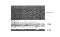
その後、黒鉛製るつぼの温度を常温まで冷却した後、黒鉛製るつぼから炭化珪素単結晶を取り出した。
得られた炭化珪素単結晶を成長方向に対して平行に切断し、その切断面を顕微鏡観察した。図3(a)はその切断面を示す顕微鏡写真であり、種結晶と炭化珪素単結晶との境界部分を示すものである。図3(a)に示すように、炭化珪素単結晶には空洞状欠陥がほとんど発生しなかった。
Then, after cooling the temperature of the graphite crucible to room temperature, the silicon carbide single crystal was taken out from the graphite crucible.
The obtained silicon carbide single crystal was cut in parallel to the growth direction, and the cut surface was observed with a microscope. FIG. 3A is a photomicrograph showing the cut surface, and shows a boundary portion between the seed crystal and the silicon carbide single crystal. As shown in FIG. 3A, almost no cavity defects occurred in the silicon carbide single crystal.
(比較例1)
種結晶にカーボン膜を形成しないほかは実施例1と同様にして、炭化珪素単結晶を形成した。
実施例1と同様に、得られた炭化珪素単結晶を成長方向に対して平行に切断し、その切断面を顕微鏡観察した。図3(b)はその切断面を示す顕微鏡写真であり、黒鉛蓋と種結晶と炭化珪素単結晶との境界部分を示すものである。図3(b)に示すように、種結晶には空洞状欠陥が数多く発生し、炭化珪素単結晶に複数の長く伸びたマイクロパイプなどの結晶内空洞欠陥を形成した。これらの空洞状欠陥およびマイクロパイプなどの結晶内空洞欠陥は、連続して続いており、種結晶と黒鉛蓋との界面から伸びていた。
(Comparative Example 1)
A silicon carbide single crystal was formed in the same manner as in Example 1 except that no carbon film was formed on the seed crystal.
In the same manner as in Example 1, the obtained silicon carbide single crystal was cut in parallel to the growth direction, and the cut surface was observed with a microscope. FIG. 3B is a photomicrograph showing the cut surface, and shows a boundary portion between the graphite lid, the seed crystal, and the silicon carbide single crystal. As shown in FIG. 3B, a large number of cavity defects were generated in the seed crystal, and a plurality of elongated cavity pipe defects such as micropipes were formed in the silicon carbide single crystal. These cavity defects and intracavity defects such as micropipes continued continuously and extended from the interface between the seed crystal and the graphite lid.
実施例1と比較例1とを比較して、種結晶と黒鉛と界面に本発明のカーボン膜を設けることにより、種結晶中の空洞状欠陥を抑制し、さらに、炭化珪素単結晶中の空洞状欠陥を抑制することができることを確認できた。 Example 1 and Comparative Example 1 are compared, and by providing the carbon film of the present invention at the interface between the seed crystal and graphite, cavity defects in the seed crystal are suppressed, and furthermore, the cavity in the silicon carbide single crystal It was confirmed that the shape defects can be suppressed.
(実施例2)
厚さ0.8mmの4H−炭化珪素単結晶の(000−1)面を成長面、(0001)面を黒鉛と接する側の面として、(0001)面にカーボン膜を形成した炭化珪素単結晶からなる成長用種結晶を用いたほかは実施例1と同様にして、炭化珪素単結晶を形成した。
得られた炭化珪素単結晶を成長方向に対して平行に切断し、その切断面を顕微鏡観察した。実施例1と同様に、炭化珪素単結晶には空洞状欠陥がほとんど発生しなかった。
これにより、炭化珪素からなる種結晶の2つの面の極性が異なる場合でも、欠陥を抑制する効果が発揮できていることを確認した。
(Example 2)
A silicon carbide single crystal in which a carbon film is formed on the (0001) plane, with the (000-1) plane of the 4H-silicon carbide single crystal having a thickness of 0.8 mm as the growth plane and the (0001) plane as the plane in contact with the graphite A silicon carbide single crystal was formed in the same manner as in Example 1 except that the seed crystal for growth consisting of was used.
The obtained silicon carbide single crystal was cut in parallel to the growth direction, and the cut surface was observed with a microscope. As in Example 1, almost no cavity defects occurred in the silicon carbide single crystal.
Thereby, even when the polarities of the two faces of the seed crystal made of silicon carbide were different, it was confirmed that the effect of suppressing defects could be exhibited.
(実施例3)
4H−炭化珪素単結晶を種結晶として用い、スパッタ前処理としてAr雰囲気、高周波電力50kWで逆スパッタを行ったほかは、実施例1と同様にして、炭化珪素単結晶を形成した。
得られた炭化珪素単結晶を成長方向に対して平行に切断し、その切断面を顕微鏡観察した。図4に示すように、炭化珪素単結晶には空洞状欠陥がほとんど発生しなかった。
(Example 3)
A silicon carbide single crystal was formed in the same manner as in Example 1 except that 4H-silicon carbide single crystal was used as a seed crystal and reverse sputtering was performed in an Ar atmosphere and high-frequency power of 50 kW as a pretreatment for sputtering.
The obtained silicon carbide single crystal was cut in parallel to the growth direction, and the cut surface was observed with a microscope. As shown in FIG. 4, almost no cavity defects occurred in the silicon carbide single crystal.
(実施例4)
4H−炭化珪素結晶を種結晶として用い、(0001)面を黒鉛と接する側の面として、この面にイオンビーム法を用いてカーボン膜を成膜した他は実施例1と同様にして、炭化珪素単結晶を形成した。なお、カーボン膜の成膜条件は、原料ガスをメタン、雰囲気圧力を1.3x10⁻²Pa、アノード電圧100Vで1時間成膜とした。
カーボン膜の膜厚は、0.4μmであった。また、X線反射率測定法を用いてカーボン膜の膜密度を測定したところ、カーボン膜の膜密度は2.5g/cm3であった。さらにまた、カーボン膜のX線回折を試みたところ、結晶構造に起因するピークが明確には現れなかった。そのため、このカーボン膜は非晶質であると判断した。
得られた炭化珪素単結晶を成長方向に対して平行に切断し、その切断面を顕微鏡観察した。炭化珪素単結晶には空洞状欠陥がほとんど発生しなかった。
Example 4
Carbonization was performed in the same manner as in Example 1 except that a 4H-silicon carbide crystal was used as a seed crystal and the (0001) plane was used as a surface in contact with graphite, and a carbon film was formed on this plane using an ion beam method. A silicon single crystal was formed. The carbon film was formed under the conditions of a source gas of methane, an atmospheric pressure of 1.3 × 10 −2 Pa, and an anode voltage of 100 V for 1 hour.
The film thickness of the carbon film was 0.4 μm. Moreover, when the film density of the carbon film was measured using the X-ray reflectivity measurement method, the film density of the carbon film was 2.5 g / cm 3 . Furthermore, when X-ray diffraction of the carbon film was attempted, a peak due to the crystal structure did not appear clearly. Therefore, this carbon film was judged to be amorphous.
The obtained silicon carbide single crystal was cut in parallel to the growth direction, and the cut surface was observed with a microscope. There were almost no cavity defects in the silicon carbide single crystal.
本発明は、炭化珪素単結晶成長用種結晶およびその製造方法並びに炭化珪素単結晶およびその製造方法に関するものであって、特に、光デバイス、高耐圧大電力用半導体素子、大電力パワーデバイス、耐高温素子、耐放射線素子、高周波素子等に使用可能な高品質な炭化珪素単結晶を製造・利用する産業において利用可能性がある。 The present invention relates to a seed crystal for silicon carbide single crystal growth and a method for producing the same, and a silicon carbide single crystal and a method for producing the same, and more particularly, to an optical device, a semiconductor device for high voltage and high power, a high power power device, The present invention is applicable to industries that manufacture and use high-quality silicon carbide single crystals that can be used for high-temperature elements, radiation-resistant elements, high-frequency elements, and the like.
1…真空容器、2…断熱材、3…加熱コイル、4…種結晶、4a…成長面、5…炭化珪素原料粉末、6…黒鉛製るつぼ、7…導入管、8…排出管、9…放射温度計、10…突出部、11…接着剤、12…カーボン膜、12b…接合面、13…炭化珪素単結晶成長用種結晶、20…空洞部、20b…内底面、20a…開口部、21…本体部、22…蓋、30…支持棒、30c…孔部。 DESCRIPTION OF SYMBOLS 1 ... Vacuum container, 2 ... Heat insulating material, 3 ... Heating coil, 4 ... Seed crystal, 4a ... Growth surface, 5 ... Silicon carbide raw material powder, 6 ... Graphite crucible, 7 ... Introducing pipe, 8 ... Discharge pipe, 9 ... Radiation thermometer, 10 ... projection, 11 ... adhesive, 12 ... carbon film, 12b ... bonding surface, 13 ... seed crystal for silicon carbide single crystal growth, 20 ... cavity, 20b ... inner bottom, 20a ... opening, 21 ... Main body, 22 ... Lid, 30 ... Support rod, 30c ... Hole.
Claims (11)
一面が昇華法により炭化珪素単結晶を成長させる成長面とされた炭化珪素からなる種結晶と、前記種結晶の前記成長面の反対側の面に形成されたカーボン膜とからなり、前記カーボン膜の膜密度が1.2〜3.3g/cm3であることを特徴とする炭化珪素単結晶成長用種結晶。 A silicon carbide single crystal growth seed crystal attached to a graphite crucible lid filled with silicon carbide raw material powder,
The carbon film is composed of a seed crystal made of silicon carbide, one surface of which is a growth surface for growing a silicon carbide single crystal by a sublimation method, and a carbon film formed on a surface opposite to the growth surface of the seed crystal. A silicon carbide single crystal growth seed crystal characterized by having a film density of 1.2 to 3.3 g / cm 3 .
A silicon carbide single crystal formed using the method for producing a silicon carbide single crystal according to claim 10 and having a micropipe density of 10 pieces / cm 2 or less.
Priority Applications (6)
| Application Number | Priority Date | Filing Date | Title |
|---|---|---|---|
| JP2008176255A JP5250321B2 (en) | 2008-07-04 | 2008-07-04 | Method for producing seed crystal for silicon carbide single crystal growth and method for producing silicon carbide single crystal |
| PCT/JP2009/060788 WO2010001709A1 (en) | 2008-07-04 | 2009-06-12 | Seed crystal for growth of silicon carbide single crystal, process for producing the same, and silicone carbide single crystal and process for producing the same |
| KR1020107027115A KR101267135B1 (en) | 2008-07-04 | 2009-06-12 | Seed crystal for growth of silicon carbide single crystal, process for producing the same, and silicone carbide single crystal and process for producing the same |
| US13/000,975 US20110111171A1 (en) | 2008-07-04 | 2009-06-12 | Seed crystal for silicon carbide single crystal growth, method for producing the seed crystal, silicon carbide single crystal, and method for producing the single crystal |
| CN200980120925.7A CN102057084B (en) | 2008-07-04 | 2009-06-12 | Seed crystal for growth of silicon carbide single crystal, process for producing the same, and silicone carbide single crystal and process for producing the same |
| EP09773287.9A EP2309039B1 (en) | 2008-07-04 | 2009-06-12 | Seed crystal for growth of silicon carbide single crystal, process for producing the same, and process for producing silicon carbide single crystal by sublimation |
Applications Claiming Priority (1)
| Application Number | Priority Date | Filing Date | Title |
|---|---|---|---|
| JP2008176255A JP5250321B2 (en) | 2008-07-04 | 2008-07-04 | Method for producing seed crystal for silicon carbide single crystal growth and method for producing silicon carbide single crystal |
Publications (2)
| Publication Number | Publication Date |
|---|---|
| JP2010013330A true JP2010013330A (en) | 2010-01-21 |
| JP5250321B2 JP5250321B2 (en) | 2013-07-31 |
Family
ID=41465812
Family Applications (1)
| Application Number | Title | Priority Date | Filing Date |
|---|---|---|---|
| JP2008176255A Active JP5250321B2 (en) | 2008-07-04 | 2008-07-04 | Method for producing seed crystal for silicon carbide single crystal growth and method for producing silicon carbide single crystal |
Country Status (6)
| Country | Link |
|---|---|
| US (1) | US20110111171A1 (en) |
| EP (1) | EP2309039B1 (en) |
| JP (1) | JP5250321B2 (en) |
| KR (1) | KR101267135B1 (en) |
| CN (1) | CN102057084B (en) |
| WO (1) | WO2010001709A1 (en) |
Cited By (7)
| Publication number | Priority date | Publication date | Assignee | Title |
|---|---|---|---|---|
| JP2011121815A (en) * | 2009-12-10 | 2011-06-23 | Sumitomo Electric Ind Ltd | Single crystal production method |
| JP2011190154A (en) * | 2010-03-16 | 2011-09-29 | Sumitomo Electric Ind Ltd | Method and apparatus for producing crystal and multilayer film |
| JP2014040333A (en) * | 2012-08-21 | 2014-03-06 | Sumitomo Electric Ind Ltd | Method for producing silicon carbide substrate |
| JP2015160750A (en) * | 2014-02-26 | 2015-09-07 | 三菱電機株式会社 | Method for manufacturing silicon carbide epitaxial wafer |
| JP2020169361A (en) * | 2019-04-03 | 2020-10-15 | 上原ネームプレート工業株式会社 | Resin member, and manufacturing method thereof |
| JP2021075427A (en) * | 2019-11-11 | 2021-05-20 | 昭和電工株式会社 | SiC SEED AND METHOD FOR MANUFACTURING SiC SINGLE CRYSTAL INGOT |
| JP2021103720A (en) * | 2019-12-25 | 2021-07-15 | 住友金属鉱山株式会社 | Epitaxial film growth wafer, epitaxial film growth method, removal method, and epitaxial wafer manufacturing method |
Families Citing this family (40)
| Publication number | Priority date | Publication date | Assignee | Title |
|---|---|---|---|---|
| WO2011065060A1 (en) | 2009-11-30 | 2011-06-03 | 住友電気工業株式会社 | Method for manufacturing single crystal |
| CN102021653B (en) * | 2010-12-30 | 2013-06-12 | 北京华进创威电子有限公司 | Method for growing silicon carbide single crystal by using high-density material block |
| US8927329B2 (en) * | 2011-03-30 | 2015-01-06 | Semiconductor Energy Laboratory Co., Ltd. | Method for manufacturing oxide semiconductor device with improved electronic properties |
| KR20120128506A (en) * | 2011-05-17 | 2012-11-27 | 엘지이노텍 주식회사 | Apparatus for attaching seed |
| KR20120131016A (en) * | 2011-05-24 | 2012-12-04 | 엘지이노텍 주식회사 | Apparatus for fabricating ingot |
| KR101897078B1 (en) * | 2011-06-01 | 2018-09-10 | 엘지이노텍 주식회사 | Apparatus and method for fabricating ingot |
| CN103088411A (en) * | 2013-01-23 | 2013-05-08 | 保定科瑞晶体有限公司 | Seed crystal fixing method for growth of silicon carbide crystals |
| CN103088426A (en) * | 2013-01-23 | 2013-05-08 | 保定科瑞晶体有限公司 | Method for reducing seed crystal growth face defects of silicon carbide crystals |
| CN104120493A (en) * | 2013-04-24 | 2014-10-29 | 梅咬清 | Method for synthesizing monocrystal silicon carbide by utilizing resistance furnace |
| CN103978746B (en) * | 2014-05-06 | 2016-06-08 | 上海天马有机发光显示技术有限公司 | A kind of film and preparation method thereof, display floater and display device |
| KR101445846B1 (en) * | 2014-05-27 | 2014-10-01 | 주식회사 케이씨엔지니어링 | A joint connector of extension electrical construction in apartment house |
| US10724151B2 (en) * | 2014-10-31 | 2020-07-28 | Sumitomo Electric Industries, Ltd. | Device of manufacturing silicon carbide single crystal |
| CN104593865A (en) * | 2014-12-25 | 2015-05-06 | 廖奇泊 | Manufacturing method of silicon carbide base crystal layer |
| KR101660032B1 (en) * | 2015-04-08 | 2016-09-27 | 한국철도기술연구원 | Carbon fiber layer with carbon coating |
| JP7333172B2 (en) * | 2015-08-20 | 2023-08-24 | インテグリス・インコーポレーテッド | Silicon carbide/graphite composites and articles and assemblies containing same |
| KR200484921Y1 (en) | 2015-09-30 | 2017-11-08 | 이호준 | Chair for combinning table |
| CN105420813A (en) * | 2015-12-22 | 2016-03-23 | 中国电子科技集团公司第二研究所 | Doping-element-free high-purity semi-insulating silicon carbide crystal growing device |
| CN105463575B (en) * | 2016-01-15 | 2019-02-19 | 北京天科合达半导体股份有限公司 | A kind of seed crystal processing method for growing silicon carbide crystal with high quality |
| CN106894089B (en) * | 2017-03-09 | 2018-03-09 | 中科钢研节能科技有限公司 | The preparation method of single-crystal silicon carbide |
| CN107190322B (en) * | 2017-04-01 | 2019-06-11 | 中国科学院上海硅酸盐研究所 | A kind of growing method of the adjustable silicon carbide polycrystalline ceramics of large scale resistivity |
| CN108048911A (en) * | 2017-12-20 | 2018-05-18 | 中国科学院上海硅酸盐研究所 | A kind of method using physical gas phase deposition technology growing large-size carborundum crystals |
| JP7258272B2 (en) * | 2018-09-06 | 2023-04-17 | 株式会社レゾナック | Thermal conductivity measuring device, heating device, thermal conductivity measuring method, and quality assurance method |
| CN111074338B (en) * | 2018-10-22 | 2022-09-20 | 赛尼克公司 | Seed crystal with protective film, method of manufacturing the same, method of attaching the same, and method of manufacturing ingot using the same |
| JP7170521B2 (en) * | 2018-12-05 | 2022-11-14 | 昭和電工株式会社 | Method for obtaining sample for evaluation of SiC single crystal |
| CN109913943A (en) * | 2019-03-05 | 2019-06-21 | 扬州港信光电科技有限公司 | A kind of manufacturing method of SiC substrate |
| TWI723415B (en) * | 2019-06-05 | 2021-04-01 | 環球晶圓股份有限公司 | Silicon carbide crystal and silicon carbide seed sheet |
| CN110306239A (en) * | 2019-07-16 | 2019-10-08 | 中国科学院上海硅酸盐研究所 | A kind of silicon carbide material seed crystal support |
| KR102268424B1 (en) * | 2019-10-22 | 2021-06-22 | 에스케이씨 주식회사 | Adhesive layer for seed crystal, method of manufacturing a laminate applied the same and method of manufacturing a wafer |
| KR102235858B1 (en) * | 2020-04-09 | 2021-04-02 | 에스케이씨 주식회사 | Manufacturing method for silicon carbide ingot and system for manufacturing silicon carbide ingot |
| CN111411395A (en) * | 2020-05-15 | 2020-07-14 | 南通大学 | Graphite crucible device for silicon carbide crystal growth and single crystal growth method thereof |
| CN113897684B (en) * | 2020-06-22 | 2023-08-08 | 比亚迪股份有限公司 | Silicon carbide seed crystal, silicon carbide seed crystal assembly, preparation method of silicon carbide seed crystal assembly and preparation method of silicon carbide crystal |
| CN113897685B (en) * | 2020-06-22 | 2023-04-07 | 比亚迪股份有限公司 | Silicon carbide seed crystal and silicon carbide seed crystal assembly |
| CN112593289A (en) * | 2021-01-29 | 2021-04-02 | 芯璨半导体科技(山东)有限公司 | Device and method for improving quality of growing silicon carbide single crystal |
| CN115467016B (en) * | 2021-06-11 | 2023-11-07 | 中电化合物半导体有限公司 | Growth assembly, apparatus and method for releasing growth stress of silicon carbide single crystal |
| CN113683964B (en) * | 2021-08-26 | 2023-03-24 | 哈尔滨科友半导体产业装备与技术研究院有限公司 | Preparation method of silicon carbide seed crystal adhesive |
| CN114059155B (en) * | 2021-11-19 | 2023-11-17 | 北京天科合达半导体股份有限公司 | Preparation method of silicon carbide crystal |
| CN114384051A (en) * | 2021-12-17 | 2022-04-22 | 山东大学 | Method for distinguishing defects in silicon carbide wafer on carbon surface of wafer |
| CN114457425B (en) * | 2022-04-12 | 2022-08-23 | 杭州乾晶半导体有限公司 | Method and device for recycling silicon carbide seed crystals |
| CN116334749B (en) * | 2023-04-18 | 2023-10-24 | 通威微电子有限公司 | Silicon carbide seed crystal bonding device and method |
| CN116837456B (en) * | 2023-07-17 | 2024-02-23 | 江苏超芯星半导体有限公司 | Seed crystal treatment method and silicon carbide crystal growth method |
Citations (5)
| Publication number | Priority date | Publication date | Assignee | Title |
|---|---|---|---|---|
| JPS6446221A (en) * | 1987-08-14 | 1989-02-20 | Hitachi Ltd | Magnetic disk |
| JPH09268096A (en) * | 1996-03-29 | 1997-10-14 | Toyota Central Res & Dev Lab Inc | Production of single crystal and seed crystal |
| JPH11189433A (en) * | 1997-12-26 | 1999-07-13 | Asahi Glass Co Ltd | Production of stain-proof glass substrate |
| JP2002201097A (en) * | 2000-12-28 | 2002-07-16 | Denso Corp | Method and apparatus of manufacturing silicon carbide, substrate for silicon carbide single crystal growing and method of heat treatment of single crystal |
| JP2003137694A (en) * | 2001-10-26 | 2003-05-14 | Nippon Steel Corp | Seed crystal for growing silicon carbide single crystal, silicon carbide single crystal ingot and method of producing the same |
Family Cites Families (11)
| Publication number | Priority date | Publication date | Assignee | Title |
|---|---|---|---|---|
| JPS5779169A (en) * | 1980-11-06 | 1982-05-18 | Sumitomo Electric Ind Ltd | Physical vapor deposition method |
| JPS60174873A (en) * | 1984-02-20 | 1985-09-09 | Hitachi Cable Ltd | Pretreatment of metallic substrate for vapor deposition |
| US5944890A (en) * | 1996-03-29 | 1999-08-31 | Denso Corporation | Method of producing single crystals and a seed crystal used in the method |
| DE19644153A1 (en) * | 1996-10-24 | 1998-04-30 | Roland Dr Gesche | Multistage low pressure plasma cleaning process |
| FR2894990B1 (en) * | 2005-12-21 | 2008-02-22 | Soitec Silicon On Insulator | PROCESS FOR PRODUCING SUBSTRATES, IN PARTICULAR FOR OPTICS, ELECTRONICS OR OPTOELECTRONICS AND SUBSTRATE OBTAINED BY SAID PROCESS |
| JP2005504885A (en) * | 2001-07-25 | 2005-02-17 | アプライド マテリアルズ インコーポレイテッド | Barrier formation using a novel sputter deposition method |
| JP2003192488A (en) * | 2001-12-20 | 2003-07-09 | Wacker Nsce Corp | Seed crystal and method for manufacturing silicon single crystal |
| JP4054197B2 (en) | 2002-02-05 | 2008-02-27 | 新日本製鐵株式会社 | Seed crystal for growing silicon carbide single crystal, method for producing the same, and method for producing silicon carbide single crystal ingot |
| JP4480349B2 (en) * | 2003-05-30 | 2010-06-16 | 株式会社ブリヂストン | Method and apparatus for producing silicon carbide single crystal |
| US7314521B2 (en) * | 2004-10-04 | 2008-01-01 | Cree, Inc. | Low micropipe 100 mm silicon carbide wafer |
| JP2008176255A (en) | 2007-01-18 | 2008-07-31 | Seiji Kiyozumi | Slide type scale table of guitar |
-
2008
- 2008-07-04 JP JP2008176255A patent/JP5250321B2/en active Active
-
2009
- 2009-06-12 EP EP09773287.9A patent/EP2309039B1/en active Active
- 2009-06-12 KR KR1020107027115A patent/KR101267135B1/en active IP Right Grant
- 2009-06-12 US US13/000,975 patent/US20110111171A1/en not_active Abandoned
- 2009-06-12 WO PCT/JP2009/060788 patent/WO2010001709A1/en active Application Filing
- 2009-06-12 CN CN200980120925.7A patent/CN102057084B/en active Active
Patent Citations (5)
| Publication number | Priority date | Publication date | Assignee | Title |
|---|---|---|---|---|
| JPS6446221A (en) * | 1987-08-14 | 1989-02-20 | Hitachi Ltd | Magnetic disk |
| JPH09268096A (en) * | 1996-03-29 | 1997-10-14 | Toyota Central Res & Dev Lab Inc | Production of single crystal and seed crystal |
| JPH11189433A (en) * | 1997-12-26 | 1999-07-13 | Asahi Glass Co Ltd | Production of stain-proof glass substrate |
| JP2002201097A (en) * | 2000-12-28 | 2002-07-16 | Denso Corp | Method and apparatus of manufacturing silicon carbide, substrate for silicon carbide single crystal growing and method of heat treatment of single crystal |
| JP2003137694A (en) * | 2001-10-26 | 2003-05-14 | Nippon Steel Corp | Seed crystal for growing silicon carbide single crystal, silicon carbide single crystal ingot and method of producing the same |
Cited By (9)
| Publication number | Priority date | Publication date | Assignee | Title |
|---|---|---|---|---|
| JP2011121815A (en) * | 2009-12-10 | 2011-06-23 | Sumitomo Electric Ind Ltd | Single crystal production method |
| JP2011190154A (en) * | 2010-03-16 | 2011-09-29 | Sumitomo Electric Ind Ltd | Method and apparatus for producing crystal and multilayer film |
| JP2014040333A (en) * | 2012-08-21 | 2014-03-06 | Sumitomo Electric Ind Ltd | Method for producing silicon carbide substrate |
| JP2015160750A (en) * | 2014-02-26 | 2015-09-07 | 三菱電機株式会社 | Method for manufacturing silicon carbide epitaxial wafer |
| JP2020169361A (en) * | 2019-04-03 | 2020-10-15 | 上原ネームプレート工業株式会社 | Resin member, and manufacturing method thereof |
| JP7352238B2 (en) | 2019-04-03 | 2023-09-28 | 上原ネームプレート工業株式会社 | Resin member and its manufacturing method |
| JP2021075427A (en) * | 2019-11-11 | 2021-05-20 | 昭和電工株式会社 | SiC SEED AND METHOD FOR MANUFACTURING SiC SINGLE CRYSTAL INGOT |
| JP7463699B2 (en) | 2019-11-11 | 2024-04-09 | 株式会社レゾナック | Method for producing SiC seed and SiC single crystal ingot |
| JP2021103720A (en) * | 2019-12-25 | 2021-07-15 | 住友金属鉱山株式会社 | Epitaxial film growth wafer, epitaxial film growth method, removal method, and epitaxial wafer manufacturing method |
Also Published As
| Publication number | Publication date |
|---|---|
| EP2309039A4 (en) | 2011-11-16 |
| US20110111171A1 (en) | 2011-05-12 |
| EP2309039A1 (en) | 2011-04-13 |
| KR101267135B1 (en) | 2013-05-24 |
| JP5250321B2 (en) | 2013-07-31 |
| CN102057084B (en) | 2013-03-27 |
| EP2309039B1 (en) | 2015-04-01 |
| WO2010001709A1 (en) | 2010-01-07 |
| CN102057084A (en) | 2011-05-11 |
| KR20110006701A (en) | 2011-01-20 |
Similar Documents
| Publication | Publication Date | Title |
|---|---|---|
| JP5250321B2 (en) | Method for producing seed crystal for silicon carbide single crystal growth and method for producing silicon carbide single crystal | |
| JP5275567B2 (en) | Tantalum carbide-coated carbon material and method for producing the same | |
| JP5377212B2 (en) | Method for producing single crystal diamond substrate | |
| US7056383B2 (en) | Tantalum based crucible | |
| WO2010024390A1 (en) | METHOD AND APPARATUS FOR MANUFACTURING SiC SINGLE CRYSTAL FILM | |
| JP2010111540A (en) | Method for growing silicon carbide single crystal, seed crystal, and silicon carbide single crystal | |
| JP2010064918A (en) | Method for producing silicon carbide single crystal, silicon carbide single crystal wafer, and silicon carbide single crystal semiconductor power device | |
| CN103160928A (en) | Seed crystal processing method for growing SiC monocrystal with high quality | |
| JP5124402B2 (en) | Method of annealing silicon carbide single crystal material | |
| JP4641536B2 (en) | Carbon composite material for reducing atmosphere furnace and method for producing the same | |
| JP4498476B2 (en) | Carbon composite material for reducing atmosphere furnace and method for producing the same | |
| JP4641533B2 (en) | Carbon composite material for reducing atmosphere furnace and method for producing the same | |
| JP4641535B2 (en) | Carbon composite material for reducing atmosphere furnace and method for producing the same | |
| KR101081598B1 (en) | Treatment method for seed and growing mehtod for single crystal | |
| JP4690367B2 (en) | Carbon composite material for reducing atmosphere furnace | |
| KR101154416B1 (en) | Single crystal method | |
| KR100782998B1 (en) | Method for growth of silicon carbide single crystal, silicon carbide seed crystal, and silicon carbide single crystal | |
| JP4641534B2 (en) | Method for producing carbon composite material for reducing atmosphere furnace | |
| KR20100032044A (en) | Treatment method for seed and growing method for single crystal | |
| JP2012001394A (en) | Substrate for growing single crystal diamond, and method for producing the single crystal diamond | |
| JP2005029459A (en) | Method for growing silicon carbide single crystal, silicon carbide seed crystal, and silicon carbide single crystal | |
| JP2013256401A (en) | Production apparatus of single crystal | |
| JP4073652B2 (en) | Silicon carbide single crystal and method for producing the same | |
| TW202432916A (en) | Base substrate and single crystal diamond laminate substrate and manufacturing method thereof | |
| CN118660994A (en) | Substrate, single crystal diamond laminate substrate, and method for producing same |
Legal Events
| Date | Code | Title | Description |
|---|---|---|---|
| A621 | Written request for application examination |
Free format text: JAPANESE INTERMEDIATE CODE: A621 Effective date: 20110405 |
|
| A131 | Notification of reasons for refusal |
Free format text: JAPANESE INTERMEDIATE CODE: A131 Effective date: 20121218 |
|
| A521 | Request for written amendment filed |
Free format text: JAPANESE INTERMEDIATE CODE: A523 Effective date: 20130213 |
|
| TRDD | Decision of grant or rejection written | ||
| A01 | Written decision to grant a patent or to grant a registration (utility model) |
Free format text: JAPANESE INTERMEDIATE CODE: A01 Effective date: 20130319 |
|
| A61 | First payment of annual fees (during grant procedure) |
Free format text: JAPANESE INTERMEDIATE CODE: A61 Effective date: 20130415 |
|
| R150 | Certificate of patent or registration of utility model |
Ref document number: 5250321 Country of ref document: JP Free format text: JAPANESE INTERMEDIATE CODE: R150 Free format text: JAPANESE INTERMEDIATE CODE: R150 |
|
| FPAY | Renewal fee payment (event date is renewal date of database) |
Free format text: PAYMENT UNTIL: 20160419 Year of fee payment: 3 |
|
| S111 | Request for change of ownership or part of ownership |
Free format text: JAPANESE INTERMEDIATE CODE: R313111 |
|
| R350 | Written notification of registration of transfer |
Free format text: JAPANESE INTERMEDIATE CODE: R350 |
|
| S531 | Written request for registration of change of domicile |
Free format text: JAPANESE INTERMEDIATE CODE: R313531 |
|
| R350 | Written notification of registration of transfer |
Free format text: JAPANESE INTERMEDIATE CODE: R350 |