JP2009518872A - 基板を処理する方法及び装置 - Google Patents
基板を処理する方法及び装置 Download PDFInfo
- Publication number
- JP2009518872A JP2009518872A JP2008544516A JP2008544516A JP2009518872A JP 2009518872 A JP2009518872 A JP 2009518872A JP 2008544516 A JP2008544516 A JP 2008544516A JP 2008544516 A JP2008544516 A JP 2008544516A JP 2009518872 A JP2009518872 A JP 2009518872A
- Authority
- JP
- Japan
- Prior art keywords
- substrate
- edge
- polishing film
- polishing
- pad
- Prior art date
- Legal status (The legal status is an assumption and is not a legal conclusion. Google has not performed a legal analysis and makes no representation as to the accuracy of the status listed.)
- Pending
Links
- 239000000758 substrate Substances 0.000 title claims abstract description 221
- 238000000034 method Methods 0.000 title claims abstract description 30
- 238000012545 processing Methods 0.000 title description 5
- 238000005498 polishing Methods 0.000 claims abstract description 204
- 239000012530 fluid Substances 0.000 claims description 68
- 238000004140 cleaning Methods 0.000 claims description 28
- 239000000126 substance Substances 0.000 claims description 12
- XLYOFNOQVPJJNP-UHFFFAOYSA-N water Substances O XLYOFNOQVPJJNP-UHFFFAOYSA-N 0.000 claims description 12
- 230000007717 exclusion Effects 0.000 claims description 11
- 239000003082 abrasive agent Substances 0.000 claims 1
- 239000000463 material Substances 0.000 description 17
- 239000012528 membrane Substances 0.000 description 8
- 239000002245 particle Substances 0.000 description 6
- 229920002635 polyurethane Polymers 0.000 description 3
- 239000004814 polyurethane Substances 0.000 description 3
- 239000004372 Polyvinyl alcohol Substances 0.000 description 2
- 230000000694 effects Effects 0.000 description 2
- 239000007788 liquid Substances 0.000 description 2
- 230000033001 locomotion Effects 0.000 description 2
- 238000005461 lubrication Methods 0.000 description 2
- 229920002451 polyvinyl alcohol Polymers 0.000 description 2
- 229920002379 silicone rubber Polymers 0.000 description 2
- 238000013519 translation Methods 0.000 description 2
- 229920002554 vinyl polymer Polymers 0.000 description 2
- DHKHKXVYLBGOIT-UHFFFAOYSA-N 1,1-Diethoxyethane Chemical compound CCOC(C)OCC DHKHKXVYLBGOIT-UHFFFAOYSA-N 0.000 description 1
- 229920004943 Delrin® Polymers 0.000 description 1
- VYPSYNLAJGMNEJ-UHFFFAOYSA-N Silicium dioxide Chemical compound O=[Si]=O VYPSYNLAJGMNEJ-UHFFFAOYSA-N 0.000 description 1
- 239000011354 acetal resin Substances 0.000 description 1
- XAGFODPZIPBFFR-UHFFFAOYSA-N aluminium Chemical compound [Al] XAGFODPZIPBFFR-UHFFFAOYSA-N 0.000 description 1
- 229910052782 aluminium Inorganic materials 0.000 description 1
- 239000008367 deionised water Substances 0.000 description 1
- 229910021641 deionized water Inorganic materials 0.000 description 1
- 238000013461 design Methods 0.000 description 1
- 239000013536 elastomeric material Substances 0.000 description 1
- 239000006260 foam Substances 0.000 description 1
- 239000011521 glass Substances 0.000 description 1
- 230000005484 gravity Effects 0.000 description 1
- 239000000314 lubricant Substances 0.000 description 1
- 238000004519 manufacturing process Methods 0.000 description 1
- TWNQGVIAIRXVLR-UHFFFAOYSA-N oxo(oxoalumanyloxy)alumane Chemical compound O=[Al]O[Al]=O TWNQGVIAIRXVLR-UHFFFAOYSA-N 0.000 description 1
- 238000007517 polishing process Methods 0.000 description 1
- 229920000642 polymer Polymers 0.000 description 1
- 229920006324 polyoxymethylene Polymers 0.000 description 1
- 238000006748 scratching Methods 0.000 description 1
- 230000002393 scratching effect Effects 0.000 description 1
- 239000004065 semiconductor Substances 0.000 description 1
- 238000007493 shaping process Methods 0.000 description 1
- HBMJWWWQQXIZIP-UHFFFAOYSA-N silicon carbide Chemical compound [Si+]#[C-] HBMJWWWQQXIZIP-UHFFFAOYSA-N 0.000 description 1
- 229910010271 silicon carbide Inorganic materials 0.000 description 1
- 229910052814 silicon oxide Inorganic materials 0.000 description 1
- 239000004945 silicone rubber Substances 0.000 description 1
- 239000007921 spray Substances 0.000 description 1
- 238000005507 spraying Methods 0.000 description 1
- 229910001220 stainless steel Inorganic materials 0.000 description 1
- 239000010935 stainless steel Substances 0.000 description 1
- 239000013589 supplement Substances 0.000 description 1
- 239000004094 surface-active agent Substances 0.000 description 1
- 238000012546 transfer Methods 0.000 description 1
Images


Classifications
-
- H—ELECTRICITY
- H01—ELECTRIC ELEMENTS
- H01L—SEMICONDUCTOR DEVICES NOT COVERED BY CLASS H10
- H01L21/00—Processes or apparatus adapted for the manufacture or treatment of semiconductor or solid state devices or of parts thereof
- H01L21/02—Manufacture or treatment of semiconductor devices or of parts thereof
- H01L21/04—Manufacture or treatment of semiconductor devices or of parts thereof the devices having potential barriers, e.g. a PN junction, depletion layer or carrier concentration layer
- H01L21/18—Manufacture or treatment of semiconductor devices or of parts thereof the devices having potential barriers, e.g. a PN junction, depletion layer or carrier concentration layer the devices having semiconductor bodies comprising elements of Group IV of the Periodic Table or AIIIBV compounds with or without impurities, e.g. doping materials
- H01L21/30—Treatment of semiconductor bodies using processes or apparatus not provided for in groups H01L21/20 - H01L21/26
- H01L21/302—Treatment of semiconductor bodies using processes or apparatus not provided for in groups H01L21/20 - H01L21/26 to change their surface-physical characteristics or shape, e.g. etching, polishing, cutting
- H01L21/304—Mechanical treatment, e.g. grinding, polishing, cutting
-
- H—ELECTRICITY
- H01—ELECTRIC ELEMENTS
- H01L—SEMICONDUCTOR DEVICES NOT COVERED BY CLASS H10
- H01L21/00—Processes or apparatus adapted for the manufacture or treatment of semiconductor or solid state devices or of parts thereof
- H01L21/02—Manufacture or treatment of semiconductor devices or of parts thereof
- H01L21/02002—Preparing wafers
- H01L21/02005—Preparing bulk and homogeneous wafers
- H01L21/02008—Multistep processes
- H01L21/0201—Specific process step
- H01L21/02021—Edge treatment, chamfering
-
- B—PERFORMING OPERATIONS; TRANSPORTING
- B24—GRINDING; POLISHING
- B24B—MACHINES, DEVICES, OR PROCESSES FOR GRINDING OR POLISHING; DRESSING OR CONDITIONING OF ABRADING SURFACES; FEEDING OF GRINDING, POLISHING, OR LAPPING AGENTS
- B24B21/00—Machines or devices using grinding or polishing belts; Accessories therefor
- B24B21/004—Machines or devices using grinding or polishing belts; Accessories therefor using abrasive rolled strips
-
- B—PERFORMING OPERATIONS; TRANSPORTING
- B24—GRINDING; POLISHING
- B24B—MACHINES, DEVICES, OR PROCESSES FOR GRINDING OR POLISHING; DRESSING OR CONDITIONING OF ABRADING SURFACES; FEEDING OF GRINDING, POLISHING, OR LAPPING AGENTS
- B24B9/00—Machines or devices designed for grinding edges or bevels on work or for removing burrs; Accessories therefor
- B24B9/02—Machines or devices designed for grinding edges or bevels on work or for removing burrs; Accessories therefor characterised by a special design with respect to properties of materials specific to articles to be ground
- B24B9/06—Machines or devices designed for grinding edges or bevels on work or for removing burrs; Accessories therefor characterised by a special design with respect to properties of materials specific to articles to be ground of non-metallic inorganic material, e.g. stone, ceramics, porcelain
- B24B9/065—Machines or devices designed for grinding edges or bevels on work or for removing burrs; Accessories therefor characterised by a special design with respect to properties of materials specific to articles to be ground of non-metallic inorganic material, e.g. stone, ceramics, porcelain of thin, brittle parts, e.g. semiconductors, wafers
Landscapes
- Engineering & Computer Science (AREA)
- Manufacturing & Machinery (AREA)
- Computer Hardware Design (AREA)
- Power Engineering (AREA)
- Mechanical Engineering (AREA)
- Physics & Mathematics (AREA)
- Condensed Matter Physics & Semiconductors (AREA)
- Microelectronics & Electronic Packaging (AREA)
- General Physics & Mathematics (AREA)
- Chemical & Material Sciences (AREA)
- Ceramic Engineering (AREA)
- Inorganic Chemistry (AREA)
- Mechanical Treatment Of Semiconductor (AREA)
- Grinding And Polishing Of Tertiary Curved Surfaces And Surfaces With Complex Shapes (AREA)
- Finish Polishing, Edge Sharpening, And Grinding By Specific Grinding Devices (AREA)
- Cleaning Or Drying Semiconductors (AREA)
Abstract
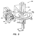
【選択図】 図5
Description
Claims (65)
- 基板の縁を研磨するように適応される装置において、
研磨膜と、
上記研磨膜の少なくとも第1の長さに張力をかけるように適応されるフレームと、
上記第1の長さの一部分に沿って上記研磨膜に対して上記基板を回転するように適応される基板回転駆動装置であって、上記研磨膜が、
上記基板に張力を付与し、
少なくとも外縁及び第1斜面を含む上記基板の縁に輪郭合わせし、
上記基板が回転されるときに上記外縁及び第1斜面を研磨する、
ように適応される基板回転駆動装置と、
を備えた装置。 - 上記フレームは、上記研磨膜のための供給スプールと巻き取りスプールを含み、更に、上記フレームは、上記基板に接触する上記研磨膜の部分を交換できるように適応される、請求項1に記載の装置。
- 上記研磨膜は、上記供給スプールと巻き取りスプールとの間で長手方向に延び、更に、上記基板回転駆動装置は、上記研磨膜の長手方向に上記基板の縁を移動する、請求項2に記載の装置。
- 上記研磨膜及び上記フレームは、交換可能なカセットに収容される、請求項1に記載の装置。
- 上記フレームは、上記研磨膜を上記基板の外縁、第1斜面及び第2斜面に接触させるために、上記基板の外縁に接する軸の周りで上記研磨膜を角度的に並進移動するよう適応される、請求項1に記載の装置。
- 上記フレームは、更に、上記基板に対し、上記基板の縁の周りで上記研磨膜を周囲方向に回転するように適応される、請求項1に記載の装置。
- 流体供給チャンネルを更に備え、該流体供給チャンネルは、上記基板の縁へ流体を送出するように適応される、請求項1に記載の装置。
- 上記流体供給チャンネルは、更に、上記研磨膜を経て上記基板の縁に流体を送出するように適応される、請求項7に記載の装置。
- 上記流体供給チャンネルは、上記基板の縁に音波エネルギーを送出するように適応される、請求項7に記載の装置。
- 前記流体は、水及び洗浄化学物質の少なくとも1つを含む、請求項7に記載の装置。
- 基板の縁を研磨するように適応される装置において、
複数の研磨膜と、
各研磨膜の少なくとも第1の長さに沿って各研磨膜に張力をかけるよう適応される少なくとも1つのフレームと、
少なくとも1つの上記研磨膜の第1の長さの一部分に対して基板を回転して、基板に接触する研磨膜が、基板に圧力を付与し、基板の縁に輪郭合わせし、更に、基板が回転されるときに縁を研磨するように適応された基板回転駆動装置と、
を備えた装置。 - 上記複数の研磨膜は、異なる研磨材を有する膜を含む、請求項11に記載の装置。
- 上記フレームは、複数のヘッドを備え、各ヘッドは、少なくとも1つの研磨膜を支持するように適応され、更に、上記ヘッドは、支持された研磨膜を基板の縁にほぼ同時に接触させるよう適応される、請求項11に記載の装置。
- 上記フレームは、複数のヘッドを備え、各ヘッドは、少なくとも1つの研磨膜を支持するように適応され、更に、各ヘッドは、支持された研磨膜を異なる時間に基板の縁に接触保持するように適応されるパッドを含む、請求項11に記載の装置。
- 上記各ヘッドのパッドは、アクチュエータがそのパッドを押すのに応答して、回転する基板に対してヘッドの研磨膜を押し付けるように適応される、請求項14に記載の装置。
- 各研磨膜及び各ヘッドは交換可能なカセットに収容される、請求項14に記載の装置。
- 上記フレームは、更に、上記研磨膜を上記基板の外縁、第1斜面、及び第2斜面に接触させるために、上記基板の外縁に接する各軸の周りで各ヘッドの研磨膜を角度的に(angularly)並進移動するよう適応される、請求項14に記載の装置。
- 上記フレームは、更に、上記基板に対して、上記基板の縁の周りで各ヘッドの研磨膜を周囲方向に回転するように適応される、請求項14に記載の装置。
- 流体供給チャンネルを更に備え、該流体供給チャンネルは、上記基板の縁へ流体を送出するように適応される、請求項11に記載の装置。
- 流体供給チャンネルを更に備え、該流体供給チャンネルは、更に、各ヘッドの研磨膜を経て上記基板の縁へ流体を送出するように適応される、請求項14に記載の装置。
- 上記流体供給チャンネルは、上記基板の縁に音波エネルギーを送出するように適応される、請求項19に記載の装置。
- 前記流体は、水及び洗浄化学物質の少なくとも1つを含む、請求項19に記載の装置。
- 基板の縁を洗浄する方法において、
フレームで研磨膜に張力をかけるステップと、
上記研磨膜を基板の縁に対して接触させるステップと、
外縁及び少なくとも1つの斜面を含む上記基板の縁に上記研磨膜を適合させるステップと、
上記研磨膜を上記基板と接触したまま上記基板を回転するステップと、
を備えた方法。 - 水及び洗浄化学物質の少なくとも1つを、膨張可能なパッドを経て上記基板の縁に付与するステップを更に備えた、請求項23に記載の方法。
- 水及び洗浄化学物質の少なくとも1つを、上記研磨膜を経て上記基板の縁に付与するステップを更に備えた、請求項23に記載の方法。
- 付加的な研磨膜を上記基板の縁に適合させるステップを更に備えた、請求項23に記載の方法。
- 音波エネルギーを含む流体を上記基板の縁に送出するステップを更に備えた、請求項23に記載の方法。
- 上記基板の外縁に接する軸の周りで上記研磨膜を角度的に並進移動するステップを更に備えた、請求項23に記載の方法。
- 上記基板に対し、上記基板の縁の周りで上記研磨膜を周囲方向に回転するステップを更に備えた、請求項23に記載の方法。
- 基板の縁を研磨するよう適応される装置において、
研磨側及び第2の側部を有する研磨膜と、
上記研磨膜の第2の側部に隣接して配置された膨張可能なパッドと、
上記研磨膜及び膨張可能なパッドを支持するように適応されるフレームと、
上記研磨膜の研磨側に対して上記基板を回転するよう適応される基板回転駆動装置と、
を備え、上記研磨膜は、上記基板の縁と上記膨張可能なパッドとの間に配置されて、上記研磨膜が上記基板の縁に接触した状態で上記膨張可能なパッド及び上記研磨膜が上記基板の縁に輪郭合わせするようにした装置。 - 上記膨張可能なパッドは、選択的に膨張可能である、請求項30に記載の装置。
- 上記基板の縁は、外縁及び少なくとも1つの斜面を含み、更に、上記膨張可能なパッドは、これが膨張して、この膨張可能なパッド及び上記研磨膜が上記外縁及び上記少なくとも1つの斜面に輪郭合わせするように適応される、請求項31に記載の装置。
- 上記基板の縁は、外縁、第1斜面及び第2斜面を含み、
上記基板は、デバイス領域及び除外領域を含み、
上記膨張可能なパッドは、これが選択的に膨張して、この膨張可能なパッド及び上記研磨膜が、上記外縁、第1斜面、第2斜面及び除外領域の1つ以上に選択的に輪郭合わせするように適応される、請求項31に記載の装置。 - 上記膨張可能なパッド及び上記研磨膜は、上記デバイス領域に接触することが阻止される、請求項33に記載の装置。
- 上記研磨膜、上記膨張可能なパッド、及び上記フレームは、交換可能なカセットに収容される、請求項30に記載の装置。
- 上記フレームは、更に、上記基板の縁に接する軸の周りで上記研磨膜を角度的に並進移動するように適応される、請求項30に記載の装置。
- 上記フレームは、更に、上記基板に対し、上記基板の縁の周りで上記研磨膜を周囲方向に回転するように適応される、請求項30に記載の装置。
- 流体供給チャンネルを更に備え、該流体供給チャンネルは、水及び洗浄化学物質の少なくとも1つを上記基板の縁へ送出するように適応される、請求項30に記載の装置。
- 上記流体供給チャンネルは、更に、上記研磨膜を経て上記基板の縁に流体を送出するように適応される、請求項38に記載の装置。
- 上記流体供給チャンネルは、更に、上記膨張可能なパッドを経て上記基板の縁に流体を送出するように適応される、請求項38に記載の装置。
- 上記膨張可能なパッドは、浸透性があり、流体で膨張できる、請求項40に記載の装置。
- 上記流体供給チャンネルは、上記基板の縁に音波エネルギーを送出するように適応される、請求項38に記載の装置。
- 基板の縁を洗浄する方法において、
研磨膜を支持するステップと、
上記研磨膜を基板の縁に対して接触させるステップと、
外縁及び少なくとも1つの斜面を含む上記基板の縁に上記研磨膜を適合させるステップと、
上記研磨膜を上記基板に接触したままで上記基板を回転するステップと、
を備えた方法。 - 研磨膜を適合させる上記ステップは、フレームにおいて上記研磨膜に張力をかけることを含む、請求項43に記載の方法。
- 研磨膜を適合させる上記ステップは、膨張可能なパッドで上記基板の縁に対して上記研磨膜を押し付けることを含む、請求項43に記載の方法。
- 上記膨張可能なパッドを調整することによって上記基板の縁に対する上記研磨膜の適合具合を調整するステップを更に備えた、請求項45に記載の方法。
- 上記膨張可能なパッドを経て上記基板の縁に水及び洗浄化学物質の少なくとも1つを付与するステップを更に備えた、請求項45に記載の方法。
- 上記研磨膜を経て上記基板の縁に水及び洗浄化学物質の少なくとも1つを付与するステップを更に備えた、請求項45に記載の方法。
- 上記基板の縁に付加的な研磨膜を適合させるステップを更に備えた、請求項45に記載の方法。
- 音波エネルギーを含む流体を上記基板の縁に配布するステップを更に備えた、請求項45に記載の方法。
- 上記基板の外縁に接する軸の周りで上記研磨膜を角度的に並進移動するステップを更に備えた、請求項45に記載の方法。
- 上記基板に対し、上記基板の縁の周りで上記研磨膜を周囲方向に回転するステップを更に備えた、請求項45に記載の方法。
- 基板の縁を研磨するように適応される装置において、
研磨材側及び後ろ側を有する研磨膜と、
上記研磨膜の後ろ側に隣接して配置された輪郭合わせされたパッドと、
上記研磨膜及び上記輪郭合わせされたパッドを支持するように適応されるフレームと、
上記研磨膜の上記研磨側に対して上記基板を回転するように適応される基板回転駆動装置と、
を備え、
上記研磨膜は、上記基板の縁と上記輪郭合わせされたパッドとの間に配置され、上記研磨膜が上記基板の縁に接触した状態で上記輪郭合わせされたパッド及び上記研磨膜が上記基板の縁に輪郭合わせするようにした装置。 - 上記基板の縁は、外縁及び少なくとも1つの斜面を含み、
上記輪郭合わせされたパッドは、上記外縁及び少なくとも1つの斜面に対して上記研磨膜を輪郭合わせするように適応される、請求項53に記載の装置。 - 上記基板の縁は、外縁、第1斜面及び第2斜面を含み、
上記基板は、デバイス領域及び除外領域を含み、
上記輪郭合わせされたパッドは、上記研磨膜を、上記外縁、第1斜面、第2斜面、及び除外領域の1つ以上に輪郭合わせするように適応される、請求項53に記載の装置。 - 上記輪郭合わせされたパッド及び上記研磨膜は、上記デバイス領域に接触することが阻止される、請求項55に記載の装置。
- 上記研磨膜、上記輪郭合わせされたパッド及び上記フレームは、交換可能なカセットに収容される、請求項53に記載の装置。
- 上記フレームは、更に、上記基板の縁に接する軸の周りで上記研磨膜を角度的に並進移動するように適応される、請求項53に記載の装置。
- 上記フレームは、更に、上記基板に対し、上記基板の縁の周りで上記研磨膜を周囲方向に回転するように適応される、請求項53に記載の装置。
- 流体供給チャンネルを更に備え、該流体供給チャンネルは、水及び洗浄化学物質の少なくとも1つを上記基板の縁へ送出するように適応される、請求項53に記載の装置。
- 上記流体供給チャンネルは、更に、上記研磨膜を経て上記基板の縁に流体を送出するように適応される、請求項60に記載の装置。
- 上記流体供給チャンネルは、更に、上記輪郭合わせされたパッドを経て上記基板の縁に流体を送出するように適応される、請求項60に記載の装置。
- 上記輪郭合わせされたパッドは、浸透性のものであり、流体で膨張できる、請求項62に記載の装置。
- 上記流体供給チャンネルは、上記基板の縁に音波エネルギーを送出するように適応される、請求項60に記載の装置。
- 上記輪郭合わせされたパッドは、流体を受け取り、その流体を上記研磨膜に付与するように適応される、請求項53に記載の装置。
Applications Claiming Priority (3)
| Application Number | Priority Date | Filing Date | Title |
|---|---|---|---|
| US11/298,555 US20070131653A1 (en) | 2005-12-09 | 2005-12-09 | Methods and apparatus for processing a substrate |
| US11/299,295 US7993485B2 (en) | 2005-12-09 | 2005-12-09 | Methods and apparatus for processing a substrate |
| PCT/US2006/046765 WO2007070353A2 (en) | 2005-12-09 | 2006-12-07 | Methods and apparatus for processing a substrate |
Related Child Applications (1)
| Application Number | Title | Priority Date | Filing Date |
|---|---|---|---|
| JP2012100094A Division JP2012183637A (ja) | 2005-12-09 | 2012-04-25 | 基板を処理する方法及び装置 |
Publications (2)
| Publication Number | Publication Date |
|---|---|
| JP2009518872A true JP2009518872A (ja) | 2009-05-07 |
| JP2009518872A5 JP2009518872A5 (ja) | 2011-10-20 |
Family
ID=38163413
Family Applications (2)
| Application Number | Title | Priority Date | Filing Date |
|---|---|---|---|
| JP2008544516A Pending JP2009518872A (ja) | 2005-12-09 | 2006-12-07 | 基板を処理する方法及び装置 |
| JP2012100094A Pending JP2012183637A (ja) | 2005-12-09 | 2012-04-25 | 基板を処理する方法及び装置 |
Family Applications After (1)
| Application Number | Title | Priority Date | Filing Date |
|---|---|---|---|
| JP2012100094A Pending JP2012183637A (ja) | 2005-12-09 | 2012-04-25 | 基板を処理する方法及び装置 |
Country Status (5)
| Country | Link |
|---|---|
| EP (1) | EP1976806A4 (ja) |
| JP (2) | JP2009518872A (ja) |
| KR (1) | KR101236855B1 (ja) |
| TW (1) | TWI362697B (ja) |
| WO (1) | WO2007070353A2 (ja) |
Cited By (3)
| Publication number | Priority date | Publication date | Assignee | Title |
|---|---|---|---|---|
| JP2012231191A (ja) * | 2007-12-03 | 2012-11-22 | Ebara Corp | 研磨装置および研磨方法 |
| JP2017087305A (ja) * | 2015-11-02 | 2017-05-25 | 日本電気硝子株式会社 | 円板状ワークの研磨加工方法及び研磨加工装置 |
| JP6414353B1 (ja) * | 2018-03-27 | 2018-10-31 | 株式会社不二越 | フィルムラップ加工装置 |
Families Citing this family (7)
| Publication number | Priority date | Publication date | Assignee | Title |
|---|---|---|---|---|
| US7993485B2 (en) | 2005-12-09 | 2011-08-09 | Applied Materials, Inc. | Methods and apparatus for processing a substrate |
| US7976361B2 (en) | 2007-06-29 | 2011-07-12 | Ebara Corporation | Polishing apparatus and polishing method |
| JP2014083647A (ja) * | 2012-10-25 | 2014-05-12 | Avanstrate Inc | ガラス基板研磨用磁性流動体 |
| TWI620240B (zh) * | 2013-01-31 | 2018-04-01 | 應用材料股份有限公司 | 用於化學機械平坦化後的基板清潔之方法及設備 |
| KR102229920B1 (ko) | 2013-10-25 | 2021-03-19 | 어플라이드 머티어리얼스, 인코포레이티드 | 화학 기계적 평탄화 후의 기판 버프 사전 세정을 위한 시스템, 방법 및 장치 |
| DE102015008814A1 (de) * | 2015-07-10 | 2017-01-12 | Thielenhaus Technologies Gmbh | Andrückschuh mit Expansionskammer |
| JP6920849B2 (ja) * | 2017-03-27 | 2021-08-18 | 株式会社荏原製作所 | 基板処理方法および装置 |
Citations (6)
| Publication number | Priority date | Publication date | Assignee | Title |
|---|---|---|---|---|
| JPH081494A (ja) * | 1994-06-27 | 1996-01-09 | Sanshin:Kk | ウエハー材縁端部研磨装置 |
| JP2002154041A (ja) * | 2000-11-17 | 2002-05-28 | I M T Kk | 研磨装置 |
| JP2002208572A (ja) * | 2001-01-09 | 2002-07-26 | Ebara Corp | 研磨装置 |
| JP2004241434A (ja) * | 2003-02-03 | 2004-08-26 | Ebara Corp | 基板処理装置 |
| JP2005186176A (ja) * | 2003-12-24 | 2005-07-14 | Shinko Electric Ind Co Ltd | ウエハ端面研磨装置 |
| WO2005081301A1 (en) * | 2004-02-25 | 2005-09-01 | Ebara Corporation | Polishing apparatus and substrate processing apparatus |
Family Cites Families (4)
| Publication number | Priority date | Publication date | Assignee | Title |
|---|---|---|---|---|
| US4533399A (en) * | 1983-04-12 | 1985-08-06 | Minnesota Mining And Manufacturing Company | Contact lens cleaning method |
| JP2924890B2 (ja) * | 1998-04-20 | 1999-07-26 | トヨタ自動車株式会社 | 研摩方法 |
| US6629875B2 (en) * | 2000-01-28 | 2003-10-07 | Accretech Usa, Inc. | Machine for grinding-polishing of a water edge |
| US6622334B1 (en) * | 2000-03-29 | 2003-09-23 | International Business Machines Corporation | Wafer edge cleaning utilizing polish pad material |
-
2006
- 2006-12-07 EP EP06844980A patent/EP1976806A4/en not_active Withdrawn
- 2006-12-07 WO PCT/US2006/046765 patent/WO2007070353A2/en active Application Filing
- 2006-12-07 KR KR1020087015337A patent/KR101236855B1/ko not_active IP Right Cessation
- 2006-12-07 JP JP2008544516A patent/JP2009518872A/ja active Pending
- 2006-12-08 TW TW095146154A patent/TWI362697B/zh not_active IP Right Cessation
-
2012
- 2012-04-25 JP JP2012100094A patent/JP2012183637A/ja active Pending
Patent Citations (6)
| Publication number | Priority date | Publication date | Assignee | Title |
|---|---|---|---|---|
| JPH081494A (ja) * | 1994-06-27 | 1996-01-09 | Sanshin:Kk | ウエハー材縁端部研磨装置 |
| JP2002154041A (ja) * | 2000-11-17 | 2002-05-28 | I M T Kk | 研磨装置 |
| JP2002208572A (ja) * | 2001-01-09 | 2002-07-26 | Ebara Corp | 研磨装置 |
| JP2004241434A (ja) * | 2003-02-03 | 2004-08-26 | Ebara Corp | 基板処理装置 |
| JP2005186176A (ja) * | 2003-12-24 | 2005-07-14 | Shinko Electric Ind Co Ltd | ウエハ端面研磨装置 |
| WO2005081301A1 (en) * | 2004-02-25 | 2005-09-01 | Ebara Corporation | Polishing apparatus and substrate processing apparatus |
Cited By (3)
| Publication number | Priority date | Publication date | Assignee | Title |
|---|---|---|---|---|
| JP2012231191A (ja) * | 2007-12-03 | 2012-11-22 | Ebara Corp | 研磨装置および研磨方法 |
| JP2017087305A (ja) * | 2015-11-02 | 2017-05-25 | 日本電気硝子株式会社 | 円板状ワークの研磨加工方法及び研磨加工装置 |
| JP6414353B1 (ja) * | 2018-03-27 | 2018-10-31 | 株式会社不二越 | フィルムラップ加工装置 |
Also Published As
| Publication number | Publication date |
|---|---|
| EP1976806A2 (en) | 2008-10-08 |
| TW200735200A (en) | 2007-09-16 |
| EP1976806A4 (en) | 2011-08-10 |
| WO2007070353A3 (en) | 2007-11-29 |
| KR20080075001A (ko) | 2008-08-13 |
| WO2007070353A2 (en) | 2007-06-21 |
| JP2012183637A (ja) | 2012-09-27 |
| KR101236855B1 (ko) | 2013-02-26 |
| TWI362697B (en) | 2012-04-21 |
Similar Documents
| Publication | Publication Date | Title |
|---|---|---|
| US7993485B2 (en) | Methods and apparatus for processing a substrate | |
| US20070131653A1 (en) | Methods and apparatus for processing a substrate | |
| JP2012183637A (ja) | 基板を処理する方法及び装置 | |
| US20090036042A1 (en) | Methods and apparatus for polishing an edge of a substrate | |
| US20080293335A1 (en) | Methods and apparatus for substrate edge polishing using a polishing arm | |
| US6358127B1 (en) | Method and apparatus for planarizing and cleaning microelectronic substrates | |
| US20080293331A1 (en) | Methods and apparatus for low cost and high performance polishing tape for substrate bevel and edge polishing in seminconductor manufacturing | |
| US20080293344A1 (en) | Methods and apparatus for polishing a notch of a substrate using a polishing pad | |
| US20080293334A1 (en) | Methods and apparatus for using a bevel polishing head with an efficient tape routing arrangement | |
| US20080293341A1 (en) | Methods and apparatus for using a rolling backing pad for substrate polishing | |
| US8506362B2 (en) | Polishing apparatus and polishing method | |
| JP2007075943A (ja) | 角形状基板の両面研磨装置および両面研磨方法 | |
| US10665480B2 (en) | Planarizing processing method and planarizing processing device | |
| US6419559B1 (en) | Using a purge gas in a chemical mechanical polishing apparatus with an incrementally advanceable polishing sheet | |
| JP4257017B2 (ja) | ウェーハの研磨装置 | |
| US20100105291A1 (en) | Methods and apparatus for polishing a notch of a substrate |
Legal Events
| Date | Code | Title | Description |
|---|---|---|---|
| A521 | Written amendment |
Free format text: JAPANESE INTERMEDIATE CODE: A523 Effective date: 20090826 |
|
| A621 | Written request for application examination |
Free format text: JAPANESE INTERMEDIATE CODE: A621 Effective date: 20090826 |
|
| RD03 | Notification of appointment of power of attorney |
Free format text: JAPANESE INTERMEDIATE CODE: A7423 Effective date: 20101130 |
|
| RD04 | Notification of resignation of power of attorney |
Free format text: JAPANESE INTERMEDIATE CODE: A7424 Effective date: 20101210 |
|
| A521 | Written amendment |
Free format text: JAPANESE INTERMEDIATE CODE: A523 Effective date: 20110905 |
|
| A871 | Explanation of circumstances concerning accelerated examination |
Free format text: JAPANESE INTERMEDIATE CODE: A871 Effective date: 20110905 |
|
| A975 | Report on accelerated examination |
Free format text: JAPANESE INTERMEDIATE CODE: A971005 Effective date: 20110927 |
|
| A131 | Notification of reasons for refusal |
Free format text: JAPANESE INTERMEDIATE CODE: A131 Effective date: 20111025 |
|
| A601 | Written request for extension of time |
Free format text: JAPANESE INTERMEDIATE CODE: A601 Effective date: 20120123 |
|
| A602 | Written permission of extension of time |
Free format text: JAPANESE INTERMEDIATE CODE: A602 Effective date: 20120130 |
|
| A521 | Written amendment |
Free format text: JAPANESE INTERMEDIATE CODE: A523 Effective date: 20120425 |
|
| A131 | Notification of reasons for refusal |
Free format text: JAPANESE INTERMEDIATE CODE: A131 Effective date: 20120703 |
|
| RD04 | Notification of resignation of power of attorney |
Free format text: JAPANESE INTERMEDIATE CODE: A7424 Effective date: 20120925 |
|
| A02 | Decision of refusal |
Free format text: JAPANESE INTERMEDIATE CODE: A02 Effective date: 20121127 |