JP2009295274A - Semiconductor device - Google Patents
Semiconductor device Download PDFInfo
- Publication number
- JP2009295274A JP2009295274A JP2009214762A JP2009214762A JP2009295274A JP 2009295274 A JP2009295274 A JP 2009295274A JP 2009214762 A JP2009214762 A JP 2009214762A JP 2009214762 A JP2009214762 A JP 2009214762A JP 2009295274 A JP2009295274 A JP 2009295274A
- Authority
- JP
- Japan
- Prior art keywords
- refresh
- circuit
- address
- power supply
- voltage
- Prior art date
- Legal status (The legal status is an assumption and is not a legal conclusion. Google has not performed a legal analysis and makes no representation as to the accuracy of the status listed.)
- Pending
Links
Images


Abstract
Description
この発明は、半導体装置に関し、特に、保持データのリフレッシュが必要なダイナミック型半導体装置においてスリープモードまたはパワーダウンモードなどのデータ保持を行なうリフレッシュモード時における消費電流を誤動作を生じさせることなく低減するための構成に関する。より特定的には、ロジックとダイナミック・ランダム・アクセス・メモリとが同一半導体チップ上に集積化されたロジック混載メモリのリフレッシュモード時の消費電流を低減するための構成に関する。 The present invention relates to a semiconductor device, and more particularly to reducing current consumption without causing malfunction in a refresh mode in which data is retained in a sleep mode or a power-down mode in a dynamic semiconductor device that requires refresh of retained data. Concerning the configuration of More specifically, the present invention relates to a configuration for reducing current consumption in a refresh mode of a logic embedded memory in which a logic and a dynamic random access memory are integrated on the same semiconductor chip.
従来のCMOS半導体装置においては、高密度高集積化のために、トランジスタサイズ、特にMOSトランジスタ(絶縁ゲート型電界効果トランジスタ)のゲート長が短くされる。このような微細化されたトランジスタの信頼性の確保および消費電力の低減のために、電源電圧が低下される。一方、高速動作のためには、MOSトランジスタのしきい値電圧Vthの絶対値を、動作電源電圧の低下に応じて小さくする必要がある。 In a conventional CMOS semiconductor device, the transistor size, particularly the gate length of a MOS transistor (insulated gate field effect transistor), is shortened for high density and high integration. In order to ensure the reliability of such miniaturized transistors and reduce power consumption, the power supply voltage is lowered. On the other hand, for high-speed operation, it is necessary to reduce the absolute value of the threshold voltage Vth of the MOS transistor as the operating power supply voltage decreases.
しかしながら、MOSトランジスタは、オフ時においてもソース−ドレイン間にサブスレッショルド・リーク電流(以下、オフリーク電流と称す)と呼ばれる電流が流れる。しきい値電圧の絶対値を小さくした場合、このオフリーク電流が増加する。しきい値電圧の絶対値は、負の温度依存性を有しており、温度上昇とともに、その絶対値が小さくなるため、動作温度が高くなると、このオフリーク電流が増大し、大規模集積回路全体の直流電流を増加させる。特に、ダイナミック型半導体記憶装置において、スタンバイ状態時における電流(スタンバイ電流)を増大させるという問題が生じる。 However, even when the MOS transistor is off, a current called a subthreshold leakage current (hereinafter referred to as off-leakage current) flows between the source and drain. When the absolute value of the threshold voltage is reduced, this off-leakage current increases. The absolute value of the threshold voltage has a negative temperature dependency, and the absolute value decreases as the temperature rises. Therefore, when the operating temperature increases, this off-leakage current increases, and the entire large-scale integrated circuit Increase the direct current. In particular, the dynamic semiconductor memory device has a problem of increasing the current (standby current) in the standby state.
高速動作性を損なうことなくスタンバイ時の消費電流を低減するために、従来からたとえば特許文献1(特開平6−237164号公報)および非特許文献1(伊藤著、「超LSIメモリ」、1994、培風館発行)などに示されるように、階層電源構成またはMT−CMOS(マルチスレッショルド−CMOS)構成が提案されている。 In order to reduce current consumption during standby without impairing high-speed operability, for example, Patent Document 1 (Japanese Patent Laid-Open No. 6-237164) and Non-Patent Document 1 (written by Ito, “VLSI LSI”, 1994, A hierarchical power supply configuration or an MT-CMOS (multi-threshold-CMOS) configuration has been proposed, as shown in (published by Baifukan).
図60は、従来のMT−CMOS構成の一例を示す図である。図60においては、内部回路として、5段の縦列接続されるCMOSインバータIV1−IV5を示す。初段のインバータIV1へ与えられる入力信号INは、スタンバイサイクル時においては、Lレベルである。CMOSインバータIV1〜IV5は、それぞれ同一構成を有し、PチャネルMOSトランジスタPTとNチャネルMOSトランジスタNTを含む。これらのMOSトランジスタPTおよびNTは、しきい値電圧の絶対値が小さな低しきい値電圧(L−Vth)MOSトランジスタである。 FIG. 60 is a diagram showing an example of a conventional MT-CMOS configuration. In FIG. 60, CMOS inverters IV1-IV5 connected in five stages in cascade are shown as internal circuits. Input signal IN applied to first-stage inverter IV1 is at the L level in the standby cycle. CMOS inverters IV1 to IV5 have the same configuration, and include P channel MOS transistor PT and N channel MOS transistor NT. These MOS transistors PT and NT are low threshold voltage (L-Vth) MOS transistors having a small absolute value of the threshold voltage.
これらのインバータIV1〜IV5に対し、電源電圧Vccを受ける主電源線1と、この主電源線1にリークカット用のPチャネルMOSトランジスタPQを介して結合されるサブ電源線3と、接地電圧Vssを伝達する主接地線2と、主接地線2に、リークカット用NチャネルMOSトランジスタNQを介して接続されるサブ接地線4が設けられる。リークカット用MOSトランジスタPQおよびNQは、そのしきい値電圧の絶対値が、MOSトランジスタPTおよびNTのしきい値電圧の絶対値よりも大きく設定されるM−VthMOSトランジスタで構成される。
For these inverters IV1-IV5, main
MOSトランジスタPQは、そのゲートに制御信号/φを受け、MOSトランジスタNQはゲートに、制御信号φを受ける。制御信号φは、内部回路が動作するアクティブサイクル時においてはHレベルとなり、内部回路が待機状態となるスタンバイサイクル時においてはLレベルとなる。一方、制御信号/φは、アクティブサイクル時にLレベルとなり、スタンバイサイクル時にHレベルとなる。 MOS transistor PQ receives control signal / φ at its gate, and MOS transistor NQ receives control signal φ at its gate. Control signal φ is at the H level during an active cycle in which the internal circuit operates, and is at the L level during a standby cycle in which the internal circuit is in a standby state. On the other hand, control signal / φ is at the L level during the active cycle and at the H level during the standby cycle.
内部回路において奇数段のインバータIV1、IV3、およびIV5…は、PチャネルMOSトランジスタPTのソースが主電源線1に接続され、NチャネルMOSトランジスタNTのソースがサブ接地線4に接続される。偶数段のインバータIV2、IV4、…は、PチャネルMOSトランジスタPTのソースがサブ電源線3に接続され、NチャネルMOSトランジスタNTのソースが主接地線2に接続される。次に、この図60に示すMT−CMOS構成の動作について図61に示す信号波形図を参照して簡単に説明する。
In the internal circuit, odd-numbered inverters IV1, IV3, IV5... Have the source of P channel MOS transistor PT connected to main
スタンバイサイクル時においては、制御信号φはLレベルであり、また制御信号/φはHレベルである。また、入力信号INは、Lレベルである。この状態においては、リークカット用MOSトランジスタPQおよびNQがオフ状態となる。一方、奇数段のインバータIV1、IV3およびIV5は、その入力信号INがLレベルであるため、内部においてPチャネルMOSトランジスタPTがオン状態、NチャネルMOSトランジスタNTがオフ状態となる。PチャネルMOSトランジスタPTは、主電源線1にそのソースが接続されており、一方NチャネルMOSトランジスタNTは、サブ接地線4にそのソースが接続されている。PチャネルMOSトランジスタPTは、対応の出力ノード(ドレイン)へ主電源線1上の電源電圧Vccレベルの電圧を伝達すると、ソースおよびドレイン間電圧が等しくなり、非導通状態となる。一方、NチャネルMOSトランジスタNTは、ゲートにLレベルの信号を受けており、オフリーク電流を生じさせる。このサブ接地線4は、比較的高いしきい値電圧M−Vthを有するリークカット用MOSトランジスタNQを介して主接地線2に接続されている。したがって、インバータIV1、IV3およびIV5…からのオフリーク電流がサブ接地線4に電流が流れても、このリークカット用MOSトランジスタNQはこれらのオフリーク電流をすべて放電することができず、サブ接地線4上の電圧レベルSVssが接地電圧Vssよりも高くなる。このサブ接地線4上の電圧SVssは、リークカット用MOSトランジスタNQの放電するリーク電流量と、内部回路に含まれるインバータ段からのオフリーク電流の総和との関係により最終的に決定される。サブ接地線4上の電圧SVssが接地電圧Vssよりも高くなると、奇数段のインバータIV1、IV3、IV5、…においてNチャネルMOSトランジスタNTのゲート−ソース間が逆バイアス状態に設定され、オフリーク電流がさらに低減される。
In the standby cycle, control signal φ is at L level and control signal / φ is at H level. The input signal IN is at L level. In this state, leak cut MOS transistors PQ and NQ are turned off. On the other hand, since odd number of inverters IV1, IV3 and IV5 have an input signal IN at L level, P channel MOS transistor PT is turned on and N channel MOS transistor NT is turned off. P channel MOS transistor PT has its source connected to main
一方、偶数段のインバータIV2、IV4、…においては、入力信号がHレベルである。これらの偶数段のインバータIV2、IV4、…においては、PチャネルMOSトランジスタPTのソースがサブ電源線3に接続され、NチャネルMOSトランジスタNTのソースが主接地線2に接続される。したがって、偶数段のインバータIV2、IV4、…においては、NチャネルMOSトランジスタはソースおよびドレインが接地電圧Vssレベルとなって非導通状態となり、オフリーク電流は生じない。一方、PチャネルMOSトランジスタPTが、オフリーク電流を生じさせる。主電源線1とサブ電源線3の間には、比較的しきい値電圧の絶対値(M−Vth)大きいリークカット用MOSトランジスタPQが設けられている。したがって、この主電源線1からサブ電源線3へのリーク電流量がリークカット用MOSトランジスタPQにより決定され、サブ電源線3上の電圧SVccは、電源電圧Vccレベルよりも低下する。このサブ電源線3上の電圧SVccの電圧レベルは、最終的にリークカット用MOSトランジスタPQの供給するリーク電流と偶数段のインバータIV2、IV4、…におけるオフリーク電流の総和との関係により決定される。電圧SVccが電源電圧Vccよりも低くなると、偶数段のインバータIV2、IV4…において、PチャネルMOSトランジスタPTのゲート−ソース間が逆バイアス状態に設定され、オフリーク電流がさらに低減される。
On the other hand, in the even-numbered inverters IV2, IV4,..., The input signal is at the H level. In these even-stage inverters IV2, IV4,..., The source of P channel MOS transistor PT is connected to sub
アクティブサイクル時においては、制御信号φがHレベルとなり、一方、制御信号/φがLレベルとなり、リークカット用MOSトランジスタPQおよびNQがオン状態となり、主電源線1がサブ電源線3に接続され、主接地線2がサブ接地線4に接続される。これにより、サブ電源線3上の電圧SVccが電源電圧Vccレベルとなり、またサブ接地線4上の電圧SVssが接地電圧Vssレベルとなる。このアクティブサイクル時において、入力信号INが動作状態に応じて適当に変化する。内部回路を構成するインバータIV1〜IV5、…のMOSトランジスタは低しきい値電圧MOSトランジスタであり、高速で動作する。このとき、リークカット用MOSトランジスタPQおよびNQは、その電流供給能力は、この内部回路の動作を十分に保証することができるように大きい値に設定される。
In the active cycle, control signal φ is at H level, while control signal / φ is at L level, leakage cut MOS transistors PQ and NQ are turned on, and main
電源線を主電源線およびサブ電源線および接地線を主接地線、サブ接地線との階層構造とすることにより、スタンバイサイクル時において、電源線/接地線のインピーダンスを高くしてリーク電流を低減し、一方、アクティブサイクル時においては、この電源線/接地線のインピーダンスを小さくして、内部回路の低しきい値電圧MOSトランジスタにより高速動作を実現する。これにより、スタンバイサイクル時の消費電流を低減しかつ高速動作する半導体回路装置を実現することを図る。 The power supply line has a hierarchical structure with the main power supply line, sub power supply line, and ground line as the main ground line and sub ground line, thereby increasing the impedance of the power supply line / ground line and reducing leakage current during the standby cycle. On the other hand, during the active cycle, the impedance of the power line / ground line is reduced, and high speed operation is realized by the low threshold voltage MOS transistor of the internal circuit. Thus, it is intended to realize a semiconductor circuit device that reduces current consumption during a standby cycle and operates at high speed.
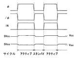
従来のMT−CMOS構成の場合、アクティブサイクルが始まるときに、制御信号φおよび/φがそれぞれHレベルおよびLレベルへ駆動され、応じて図60に示すリークカット用MOSトランジスタPQおよびNQがオン状態となる。したがって、アクティブサイクルが始まってから、サブ電源線3およびサブ接地線4上の電圧SVccおよびSVssが、それぞれ電源電圧Vccおよび接地電圧Vssに到達して安定化するまでにある時間が必要となる。サブ電源線3およびサブ接地線4上の電圧SVccおよびSVssが不安定な状態においては、内部回路は動作することができない。したがって、図62に示すように、アクティブサイクルが始まってから実際に内部回路が動作するまでにある時間が必要とされ、高速動作を実現することができなくなるという問題があった。電圧SVccおよびSVssが不安定な状態で内部回路を動作させた場合、誤動作が生じる可能性があり、この電圧SVccおよびSVssが安定化に要する時間にあるマージンをもって内部回路動作開始タイミングを決定する必要がある。
In the case of the conventional MT-CMOS configuration, when the active cycle starts, control signals φ and / φ are driven to H level and L level, respectively, and accordingly, leak-cut MOS transistors PQ and NQ shown in FIG. 60 are turned on. It becomes. Therefore, after the active cycle starts, a certain time is required until voltages SVcc and SVss on sub
また、図60に示すように、従来のMT−CMOS構成においては、スタンバイサイクル時における入力信号INの論理レベルが予め決定されている必要がある。スタンバイサイクル時の入力信号INの論理レベルに合せて、内部回路の電源線および接地線の接続先を決定する必要がある。しかしながら、ランダムロジックおよび動作条件を示すデータを格納するレジスタ回路などにおいては、スタンバイサイクル時の入力信号の論理レベルを予め決定することができず、したがって、図60に示すようなMT−CMOS構成を利用することができない。 As shown in FIG. 60, in the conventional MT-CMOS configuration, the logic level of the input signal IN in the standby cycle needs to be determined in advance. It is necessary to determine the connection destination of the power supply line and the ground line of the internal circuit in accordance with the logic level of the input signal IN during the standby cycle. However, in a register circuit or the like for storing data indicating random logic and operating conditions, the logic level of the input signal in the standby cycle cannot be determined in advance, and therefore, an MT-CMOS configuration as shown in FIG. It cannot be used.
また、半導体装置が、ダイナミック型半導体記憶装置(DRAMと以下称す)の場合、比較的長い期間にわたってアクセスがされない場合、スリープモードが設定されると、このDRAMはセルフリフレッシュモードに設定される。このセルフリフレッシュモード時においては、DRAMは、内部で、所定の周期でメモリセルデータのリフレッシュを実行する。 In the case where the semiconductor device is a dynamic semiconductor memory device (hereinafter referred to as DRAM), when access is not performed for a relatively long period, when the sleep mode is set, the DRAM is set to the self-refresh mode. In this self-refresh mode, the DRAM internally refreshes the memory cell data at a predetermined cycle.
実際にセルフリフレッシュが行なわれるときには、このDRAMは、アクティブサイクルに入り、リフレッシュが完了すると、スタンバイサイクルに入る。すなわち、DRAMは、セルフリフレッシュモードにおいて、所定の周期でアクティブサイクルに入る。したがって、このセルフリフレッシュモード時においては、単にデータ保持を行なうために、内部でメモリセルのデータのリフレッシュが行なわれており、電流が消費されるという問題が生じる。消費電流を低減するためには、このリフレッシュ間隔を長くする必要があるものの、リフレッシュ間隔を不必要に長くすると、メモリセルデータがリフレッシュ動作前に破壊され、データ保持を行なうことができなくなる。 When self-refreshing is actually performed, this DRAM enters an active cycle, and enters a standby cycle when refreshing is completed. That is, the DRAM enters an active cycle at a predetermined period in the self-refresh mode. Therefore, in the self-refresh mode, the data in the memory cell is refreshed internally in order to simply hold the data, resulting in a problem that current is consumed. In order to reduce the current consumption, it is necessary to lengthen the refresh interval. However, if the refresh interval is unnecessarily increased, the memory cell data is destroyed before the refresh operation, and data cannot be retained.
それゆえ、この発明の目的は、高速動作性を損なうことなく待機状態時の消費電流を低減することのできる半導体装置を提供することである。 Therefore, an object of the present invention is to provide a semiconductor device capable of reducing current consumption in a standby state without impairing high-speed operability.
この発明の他の目的は、セルフリフレッシュモード時の消費電流を低減することのできる半導体装置を提供することである。 Another object of the present invention is to provide a semiconductor device capable of reducing current consumption in the self-refresh mode.
この発明のさらに他の目的は通常動作およびデータ保持性能に悪影響を及ぼすことなく待機モード時の消費電流を低減することのできる半導体装置を提供することである。 Still another object of the present invention is to provide a semiconductor device capable of reducing current consumption in the standby mode without adversely affecting normal operation and data retention performance.
請求項1に係る半導体装置は、記憶データを一定期間内にリフレッシュする必要のある複数のメモリセルと、リフレッシュモード時複数のメモリセルの記憶データのリフレッシュ動作を行なうためのリフレッシュ系回路と、このリフレッシュ系回路と異なり、複数のメモリセルへのアクセスに関連する動作を少なくとも行なうための周辺回路と、リフレッシュ系回路へ動作電源電圧を供給するための第1の電源回路と、この第1の電源回路と別に設けられ、周辺回路へ動作電源電圧を供給するための第2の電源回路と、動作モード指示信号に応答して、少なくとも第2の電源回路のインピーダンスを調整するための電源制御回路を備える。この電源制御回路は、動作モード指示信号がリフレッシュモードを指定するとき第1および第2の電源回路を互いに異なる電圧供給状態に設定し、かつ動作モード指示信号がリフレッシュモードと異なるノーマルモードを指定するとき第1および第2の電源回路を同一電圧供給状態に設定するための手段を含む。
A semiconductor device according to
請求項2に係る半導体装置は、請求項1の装置において、第1の電源回路が第1の電源供給ノードと第1の電源供給線の間に接続される第1の絶縁ゲート型電界効果トランジスタを備え、第2の電源回路が第2の電源供給ノードと第2の電源供給線の間に設けられる第2の絶縁ゲート型電界効果トランジスタを備える。電源制御回路は、動作モード指示信号がリフレッシュモードを指定するとき第1の絶縁ゲート型電界効果トランジスタをオン状態に設定しかつ第2の絶縁ゲート型電界効果トランジスタをオフ状態に設定する手段を含む。
A semiconductor device according to
請求項3に係る半導体装置は、請求項1の装置において、第2の電源回路が、電源供給ノードと電源供給線との間に接続されかつ周辺回路の構成要素である絶縁ゲート型電界効果トランジスタのしきい値電圧よりも絶対値の大きなリークカット用絶縁ゲート型電界効果トランジスタを備える。電源制御回路は、動作モード指示信号がリフレッシュモードを指定するときリークカット用絶縁ゲート型電界効果トランジスタをオフ状態に設定する手段を含む。
The semiconductor device according to
請求項4に係る半導体装置は、請求項1の装置において、第2の電源回路が、電源供給ノードと電源供給線との間に接続され、周辺回路の構成要素である絶縁ゲート型電界効果トランジスタと同じしきい値電圧を有するリークカット用絶縁ゲート型電界効果トランジスタを備える。このリークカット用絶縁ゲート型電界効果トランジスタはオフ状態時のリーク電流が周辺回路の総リーク電流量よりも小さくなるようにそのサイズが調整される。また、電源制御回路は、動作モード指示信号がリフレッシュモードを指定するとき、リークカット用絶縁ゲート型電界効果トランジスタをオフ状態に設定する手段を含む。 According to a fourth aspect of the present invention, there is provided the semiconductor device according to the first aspect, wherein the second power supply circuit is connected between the power supply node and the power supply line, and is an insulated gate field effect transistor as a component of the peripheral circuit. And a leak-cut insulated gate field effect transistor having the same threshold voltage as the above. The size of the leak-cut insulated gate field effect transistor is adjusted so that the leak current in the off state is smaller than the total leak current amount of the peripheral circuit. The power supply control circuit includes means for setting the leak-cut insulated gate field effect transistor to an OFF state when the operation mode instruction signal specifies the refresh mode.
請求項5に係る半導体装置は、請求項1の装置において、第2の電源回路が、電源供給ノードと電源供給線との間に接続されるリークカット用絶縁ゲート型電界効果トランジスタを備える。周辺回路は、構成要素として絶縁ゲート型電界効果トランジスタを含む。電源制御回路が、動作モード指示信号がリフレッシュモードを指定するとき、リークカット用絶縁ゲート型電界効果トランジスタを周辺回路の絶縁ゲート型電界効果トランジスタのオフ状態よりも深いオフ状態に設定する手段を含む。 According to a fifth aspect of the present invention, in the semiconductor device according to the first aspect, the second power supply circuit includes a leak-cut insulated gate field effect transistor connected between the power supply node and the power supply line. The peripheral circuit includes an insulated gate field effect transistor as a component. The power supply control circuit includes means for setting the leak-cut insulated gate field effect transistor in an off state deeper than the off state of the peripheral gate insulated gate field effect transistor when the operation mode instruction signal specifies the refresh mode. .
請求項6に係る半導体装置は、請求項5の装置において、電源制御回路が、動作モード指示信号がリフレッシュモードを指定するとき、リークカット用絶縁ゲート型電界効果トランジスタのゲートへ電源供給ノード上の電圧よりも絶対値の大きな電圧を印加するための手段を含む。 According to a sixth aspect of the present invention, there is provided the semiconductor device according to the fifth aspect, wherein when the operation mode instruction signal designates the refresh mode, the power supply control circuit is on the power supply node to the gate of the leak-cut insulated gate field effect transistor. Means for applying a voltage having an absolute value larger than the voltage is included.
請求項7に係る半導体装置は、請求項5の装置において、電源制御回路が、ノーマルモード時よりもリフレッシュモード時リークカット用絶縁ゲート型電界効果トランジスタのバックゲートへ印加される電圧の絶対値を大きくするための手段を含む。 According to a seventh aspect of the present invention, in the semiconductor device according to the fifth aspect, the power supply control circuit determines the absolute value of the voltage applied to the back gate of the leak-cut insulated gate field effect transistor in the refresh mode rather than in the normal mode. Includes means to enlarge.
請求項8に係る半導体装置は、請求項1の装置において、第1の電源回路が、外部からの第1の電源電圧を受ける第1の電源供給ノードを備え、第2の電源回路が、外部からの第2の電源電圧を受ける第2の電源ノードと、第2の電源ノードと周辺回路に結合される電源供給線との間に設けられるリークカット用絶縁ゲート型電界効果トランジスタを備える。電源制御回路は、動作モード指示信号がリフレッシュモードを指定するとき、リークカット用絶縁ゲート型電界効果トランジスタをオフ状態に設定するための手段を含む。 According to an eighth aspect of the present invention, there is provided the semiconductor device according to the first aspect, wherein the first power supply circuit includes a first power supply node that receives a first power supply voltage from the outside, and the second power supply circuit is externally provided. A second power supply node that receives the second power supply voltage from the first power supply voltage, and a leak-cut insulated gate field effect transistor provided between the second power supply node and a power supply line coupled to the peripheral circuit. The power supply control circuit includes means for setting the leak-cut insulated gate field effect transistor to an off state when the operation mode instruction signal specifies the refresh mode.
請求項9に係る半導体装置は、請求項1の装置において、第2の電源回路が外部からの電源電圧と基準電圧とを比較し、該比較結果に従って内部電源電圧を生成して周辺回路へ印加する内部電源回路を備える。電源制御回路は、動作モード指示信号がリフレッシュモードを指定するとき、この基準電圧を外部電源電圧と異なる極性の電圧レベルに設定する手段を含む。
The semiconductor device according to
請求項10に係る半導体装置は、請求項1または8の装置がさらに、動作モード指示信号に応答して、リフレッシュ系回路が形成される半導体基板領域の電位を調整するためのウェル電位制御回路を備える。このウェル電位制御回路が、動作モード指示信号がリフレッシュモードを指定するとき、この半導体基板領域の電位の絶対値をノーマルモード時よりも大きくするための手段を含む。 According to a tenth aspect of the present invention, there is provided a semiconductor device according to the first or eighth aspect, further comprising a well potential control circuit for adjusting the potential of the semiconductor substrate region in which the refresh circuit is formed in response to the operation mode instruction signal. Prepare. The well potential control circuit includes means for making the absolute value of the potential of the semiconductor substrate region larger than that in the normal mode when the operation mode instruction signal specifies the refresh mode.
請求項11に係る半導体装置は、請求項10の装置がさらに、複数のメモリセルへアクセスして受けたデータの処理または処理後のデータの格納を行なうためのロジック回路を備える。ウェル電位制御回路は、このロジック回路が形成される半導体基板領域の電位をリフレッシュモード時、ノーマルモード時のそれよりも絶対値を大きくするための手段をさらに備える。 The semiconductor device according to an eleventh aspect of the present invention further includes a logic circuit for processing the data received by accessing the plurality of memory cells or storing the data after the processing. The well potential control circuit further includes means for increasing the absolute value of the potential of the semiconductor substrate region where the logic circuit is formed in the refresh mode and in the normal mode.
請求項12に係る半導体装置は、請求項1の装置がさらに、複数のメモリセルとデータの授受を行なうためのロジック回路と、このロジック回路へ動作電源電圧を供給するための第3の電源回路を備える。電源制御回路は、動作モード指示信号がリフレッシュモードを指定するとき、ロジック回路への動作電源電圧の供給を停止するように第3の電源回路を制御する手段を備える。 According to a twelfth aspect of the present invention, the semiconductor device according to the first aspect further includes a logic circuit for exchanging data with a plurality of memory cells, and a third power supply circuit for supplying an operating power supply voltage to the logic circuit. Is provided. The power supply control circuit includes means for controlling the third power supply circuit to stop supplying the operation power supply voltage to the logic circuit when the operation mode instruction signal specifies the refresh mode.
請求項13に係る半導体装置は、請求項10の装置において、電源制御回路が、動作モード指示信号がリフレッシュモードを示すとき、周辺回路への動作電源電圧の供給を停止するように第2の電源回路のインピーダンスを大きくするための手段を備える。 According to a thirteenth aspect of the present invention, there is provided the semiconductor device according to the tenth aspect, wherein the power supply control circuit is configured to stop the supply of the operation power supply voltage to the peripheral circuit when the operation mode instruction signal indicates the refresh mode. Means are provided for increasing the impedance of the circuit.
請求項14に係る半導体装置は、一定期間内に記憶データがリフレッシュされる複数のメモリセルと、電源供給ノードの電源電圧を受け、複数のメモリセルへのアクセス動作に関連する情報を格納するためのレジスタ回路と、このレジスタ回路に対応して設けられ、レジスタ回路の記憶情報を保持するためのレジスタキャパシタと、動作モード指示信号がリフレッシュモードを指定するとき、レジスタキャパシタの記憶情報を所定の周期でリフレッシュするための制御回路を備える。
The semiconductor device according to
請求項15に係る半導体装置は、請求項14の装置において、制御回路が、動作モード指示信号がリフレッシュモードを指定するとき、所定周期で電源供給ノードからレジスタ回路へ電源電圧を供給しかつレジスタ回路をレジスタキャパシタと結合するための手段を含む。 According to a fifteenth aspect of the present invention, there is provided the semiconductor device according to the fourteenth aspect, wherein the control circuit supplies the power supply voltage from the power supply node to the register circuit at a predetermined cycle when the operation mode instruction signal specifies the refresh mode. Means for coupling to the resistor capacitor.
請求項16に係る半導体装置は、請求項15の所定周期が、複数のメモリセルの記憶データのリフレッシュを行なう一定の周期と同じである。 In the semiconductor device according to a sixteenth aspect, the predetermined period of the fifteenth aspect is the same as a constant period for refreshing stored data of a plurality of memory cells.
請求項17に係る半導体装置は、請求項16の装置において、制御回路が、複数のメモリセルの選択されたメモリセルの記憶データのリフレッシュが行なわれている間、電源ノードからレジスタ回路へ電源電圧を供給する手段を含む。 According to a seventeenth aspect of the present invention, there is provided the semiconductor device according to the sixteenth aspect, wherein the power supply voltage is supplied from the power supply node to the register circuit while the control circuit is refreshing the data stored in the selected memory cell of the plurality of memory cells. Means for supplying.
請求項18に係る半導体装置は、請求項14の装置において、複数のメモリセルの各々が、情報を記憶するためのメモリキャパシタを含む。レジスタキャパシタは、このメモリキャパシタと、絶縁膜およびセルプレート電極が、材料および膜厚の少なくとも一方において同じである。 A semiconductor device according to an eighteenth aspect is the device according to the fourteenth aspect, wherein each of the plurality of memory cells includes a memory capacitor for storing information. In the resistor capacitor, the memory capacitor, the insulating film, and the cell plate electrode are the same in at least one of material and film thickness.
請求項19に係る半導体装置は、一定期間内に記憶データがリフレッシュされかつ所定の記憶容量を有する複数のメモリセルのメモリセルアレイと、動作モード指示信号に応答してリフレッシュを行なうリフレッシュモードが指定されたときにリフレッシュを行なうリフレッシュ領域を指定するアドレスを受けて格納するための手段と、動作モード指示信号がリフレッシュモードを指定するとき、リフレッシュ領域指定アドレスが指定する領域内のメモリセルのリフレッシュを行なうようにリフレッシュアドレスを発生するためのリフレッシュアドレス発生回路と、リフレッシュモード時、所定の周期でメモリセルデータのリフレッシュを要求するリフレッシュ要求を出力するリフレッシュタイマと、リフレッシュタイマからのリフレッシュ要求に従って、リフレッシュアドレスのメモリセルの記憶データのリフレッシュを行なうためのリフレッシュ系回路とを備える。 In the semiconductor device according to claim 19, a memory cell array of a plurality of memory cells in which stored data is refreshed within a predetermined period and having a predetermined storage capacity, and a refresh mode for performing refresh in response to an operation mode instruction signal are designated. Means for receiving and storing an address designating a refresh area to be refreshed, and when the operation mode instruction signal designates the refresh mode, the memory cells in the area designated by the refresh area designating address are refreshed. A refresh address generating circuit for generating a refresh address, a refresh timer for outputting a refresh request for refreshing memory cell data in a predetermined cycle in the refresh mode, and a refresh from the refresh timer According determined, and a refresh-related circuitry for performing a refresh of the stored data of the memory cells of the refresh address.
請求項20に係る半導体装置は、請求項19の装置において複数のメモリセルは行列状に配列され、かつメモリセル行のうちデータ保持特性が劣るメモリセルが接続される特定の行に関連する特定アドレスを格納するアドレス格納手段をさらに備える。リフレッシュ系回路は、特定アドレス格納手段の格納する特定アドレスに従って、特定の行のメモリセルのリフレッシュを他の行のメモリセルのリフレッシュの回数よりも多くするリフレッシュ調整手段を備える。
A semiconductor device according to
請求項21に係る半導体装置は、請求項20の装置において、リフレッシュ調整手段が、リフレッシュタイマからのリフレッシュ要求が発生される所定の周期よりも短い周期で特定の行に対するアドレスを選択状態に設定する手段を含む。
The semiconductor device according to
請求項22に係る半導体装置は、請求項20の装置において、リフレッシュ調整手段が、リフレッシュアドレス発生回路からのリフレッシュアドレスと特定アドレス格納手段からの特定アドレスとに従って特定アドレスがリフレッシュアドレスにより指定されるとき、このリフレッシュアドレスの行および特定行をともにアドレス指定するアドレス変換手段を含む。 According to a twenty-second aspect of the present invention, in the semiconductor device according to the twenty-first aspect, when the refresh adjusting unit specifies the specific address by the refresh address according to the refresh address from the refresh address generating circuit and the specific address from the specific address storing unit. Address conversion means for addressing both the refresh address row and the specific row.
請求項23に係る半導体装置は、請求項19の装置がさらに、リフレッシュ領域アドレスに従ってリフレッシュタイマの所定の周期を調整するための手段を備える。 According to a twenty-third aspect of the present invention, there is provided the semiconductor device according to the nineteenth aspect, further comprising means for adjusting a predetermined cycle of the refresh timer in accordance with the refresh area address.
請求項24に係る半導体装置は、請求項10の装置が、さらに、動作モード指示信号に応答してリフレッシュ系回路の動作タイミングをリフレッシュモード時とノーマルモード時とで異ならせるための制御回路をさらに備える。 A semiconductor device according to a twenty-fourth aspect is the semiconductor device according to the tenth aspect, further comprising a control circuit for making the operation timing of the refresh circuit different between the refresh mode and the normal mode in response to the operation mode instruction signal. Prepare.
請求項25に係る半導体装置は、請求項24の装置において複数のメモリセルが行列状に配列される。リフレッシュ系回路は、複数のメモリセルの列に対応して設けられ、活性化時対応の列のメモリセルデータの検知および増幅を行なうためのセンスアンプ回路を備える。制御回路は動作モード指示信号がリフレッシュモードを指定するとき、センスアンプ回路の活性化タイミングをノーマルモード時の活性化タイミングよりも遅らせるための手段を含む。 A semiconductor device according to a twenty-fifth aspect is the device according to the twenty-fourth aspect, wherein a plurality of memory cells are arranged in a matrix. The refresh circuit is provided corresponding to a plurality of memory cell columns, and includes a sense amplifier circuit for detecting and amplifying memory cell data in a column corresponding to activation. The control circuit includes means for delaying the activation timing of the sense amplifier circuit from the activation timing in the normal mode when the operation mode instruction signal designates the refresh mode.
リフレッシュモード時に、周辺回路への電源供給電圧の供給を停止することにより、リフレッシュモード時における周辺回路の消費電流を低減することができる。また、ノーマルモード時においては、リフレッシュ系回路および周辺回路ともに電源電圧を供給することによりアクティブサイクルおよびスタンバイサイクルの切換時においても、電源電圧の変動は生じず、速いタイミングで内部回路動作を開始することができる。 By stopping the supply of the power supply voltage to the peripheral circuit in the refresh mode, the current consumption of the peripheral circuit in the refresh mode can be reduced. In the normal mode, the power supply voltage is supplied to both the refresh circuit and the peripheral circuit so that the power supply voltage does not fluctuate even when switching between the active cycle and the standby cycle, and the internal circuit operation is started at a fast timing. be able to.
リフレッシュモード時、レジスタ回路のデータを保持するレジスタキャパシタの記憶情報を所定周期でリフレッシュすることにより、このレジスタ回路への電源供給をリフレッシュモード時間欠的に停止させることができ、リフレッシュモード時における消費電流を低減することができる。 In the refresh mode, the storage information of the register capacitor that holds the data of the register circuit is refreshed at a predetermined cycle, so that the power supply to the register circuit can be stopped in the refresh mode time, and the consumption in the refresh mode The current can be reduced.
また、リフレッシュモード時、所定のアドレス領域のメモリセルのみリフレッシュを行なうことにより、リフレッシュされるメモリセル行の数を低減でき、応じてリフレッシュ回数を低減でき、消費電流を低減することができる。 In the refresh mode, by refreshing only memory cells in a predetermined address area, the number of memory cell rows to be refreshed can be reduced, and the number of refreshes can be reduced accordingly, thereby reducing current consumption.
以上のように、この発明に従えば、セルフリフレッシュモード(スリープモード)時における消費電流をその通常モード時のアクセス動作に悪影響を及ぼすことなく大幅に低減することができる。 As described above, according to the present invention, the current consumption in the self-refresh mode (sleep mode) can be significantly reduced without adversely affecting the access operation in the normal mode.
すなわち、請求項1に係る発明に従えば、スリープモードおよびパワーダウンモードなどの低消費電流モード時、リフレッシュ動作を行なうリフレッシュ系回路と、それ以外の周辺回路とに対し通常動作モード時には、電源線を同じ電源供給状態に設定し、かつ低消費電流モード時には、互いに異なる電源供給状態に設定しているため、低消費電流モード時、リフレッシュ系回路にのみ動作電源電圧を供給することができ、低消費電流モード時の消費電流を低減することができる。また、通常動作モード時には、動作電源電圧をともに周辺回路およびリフレッシュ系回路に供給しているため、通常動作モードのスタンバイサイクルからアクセスサイクルへの移行時動作電源電圧の変動がアクセス時間に影響を及ぼすのを防止することができ、通常動作モード時の高速アクセスを保証することができる。 In other words, according to the first aspect of the present invention, in the low power consumption mode such as the sleep mode and the power down mode, the power supply line is operated in the normal operation mode with respect to the refresh circuit for performing the refresh operation and other peripheral circuits. Are set to the same power supply state and in the low current consumption mode, they are set to different power supply states. Therefore, in the low current consumption mode, the operation power supply voltage can be supplied only to the refresh circuit. Current consumption in the current consumption mode can be reduced. In the normal operation mode, both the operation power supply voltage is supplied to the peripheral circuit and the refresh circuit, and therefore the fluctuation of the operation power supply voltage during the transition from the standby cycle to the access cycle in the normal operation mode affects the access time. Can be prevented, and high-speed access in the normal operation mode can be ensured.
請求項2に係る発明に従えば、リフレッシュ系回路および周辺回路に対する電源回路の可変インピーダンス手段をMOSトランジスタで構成し、低消費電流モード時、このリフレッシュ系回路に対するMOSトランジスタをオン状態、周辺回路に対するMOSトランジスタをオフ状態に設定しているため、周辺回路における低消費電流モード時の消費電流を抑制することができる。 According to the second aspect of the present invention, the variable impedance means of the power supply circuit for the refresh circuit and the peripheral circuit is formed of a MOS transistor, and the MOS transistor for the refresh circuit is turned on in the low current consumption mode. Since the MOS transistor is set to the off state, the current consumption in the low current consumption mode in the peripheral circuit can be suppressed.
請求項3に係る発明に従えば、周辺回路用電源回路のMOSトランジスタのしきい値電圧の絶対値を、この周辺回路のMOSトランジスタのそれよりも大きくし、低消費電流モード時この周辺回路用電源回路のMOSトランジスタをオフ状態に設定しており、確実に、低消費電流モード時のリーク電流を抑制して、消費電流を低減することができる。
According to the invention of
請求項4に係る発明に従えば、周辺回路用電源回路のMOSトランジスタを周辺回路用MOSトランジスタと同一しきい値電圧を有するように構成し、この周辺回路用電源回路のMOSトランジスタのオフ状態時のリーク電流が、周辺回路の総リーク電流量よりも小さくなるようにサイズを調整しており、低消費電流モード時、周辺回路用電源回路のMOSトランジスタをオフ状態とすることにより、周辺回路部のリーク電流が電源回路のMOSトランジスタのオフリーク電流で決定され、消費電流をより低減することができる。
According to the invention of
また、周辺回路用電源回路のMOSトランジスタおよび周辺回路のMOSトランジスタが同一しきい値電圧を有しており、サイズが異なるだけであり、同一製造工程でこれらのMOSトランジスタを形成することができる。 Further, the MOS transistors of the peripheral circuit power supply circuit and the MOS transistors of the peripheral circuit have the same threshold voltage, and are different in size, and these MOS transistors can be formed in the same manufacturing process.
請求項5に係る発明に従えば、周辺回路用電源回路のリークカットMOSトランジスタを、周辺回路のMOSトランジスタのオフ状態よりもより深いオフ状態に設定するように構成しており、この電源回路のリークカットMOSトランジスタのオフリーク電流を低減でき、低消費電流モード時の消費電流を低減することができる。
According to the invention of
請求項6に係る発明に従えば、この請求項5のリークカットMOSトランジスタのゲートへ、電源供給ノードの電圧よりも絶対値の大きな電圧を低消費電流モード時印加するように構成しており、確実に、より深いオフ状態に容易に設定することができる。
According to the invention of
請求項7に係る発明に従えば、請求項5のリークカットMOSトランジスタのバックゲート電圧を低消費電流モード時通常動作モード時によりもその絶対値を大きくしており、確実にそのしきい値電圧の絶対値をリークカットMOSトランジスタにおいて大きくでき、低しきい値電圧MOSトランジスタをリークカットMOSトランジスタとして用いても、その実効的なしきい値電圧の絶対値の増大により、確実にオフリーク電流を防止することができる。
According to the invention of
請求項8に係る発明に従えば、リフレッシュ系回路へは、外部からの電源電圧を直接供給し、一方、周辺系回路へは、リークカットMOSトランジスタを介して動作電源電圧を供給し、低消費電流モード時、このリークカットMOSトランジスタをオフ状態に設定しているため、容易に、低消費電流モード時の消費電流を低減することができる。また、リフレッシュ系回路へは、直接外部からの電源電圧が供給され、回路構成が簡略化される。 According to the eighth aspect of the present invention, the power supply voltage from the outside is directly supplied to the refresh system circuit, while the operation power supply voltage is supplied to the peripheral system circuit via the leak cut MOS transistor to reduce the consumption. Since the leak cut MOS transistor is set in the off state in the current mode, the current consumption in the low current consumption mode can be easily reduced. Further, the power supply voltage from the outside is directly supplied to the refresh system circuit, and the circuit configuration is simplified.
請求項9に係る発明に従えば、周辺系回路の電源回路が、基準電圧との比較に基づいて内部電源電圧を生成する内部電源回路で構成され、この低消費電流モード時には、基準電圧を外部電源電圧と異なる極性の電圧レベルに設定しており、内部電源回路を有する場合においても、低消費電流モード時、消費電流を低減することができる。
According to the invention of
請求項10に係る発明に従えば、リフレッシュ系回路が形成される基板領域の電位の絶対値を低消費電流モード時通常動作モード時のそれよりも大きくしており、低消費電流モード時において、リフレッシュ系回路のMOSトランジスタのしきい値電圧の絶対値を大きくでき、オフリーク電流を低減できる。
According to the invention of
請求項11に係る発明に従えば、ロジック回路が形成される基板領域の電位を低消費電流モード時通常動作モード時のそれよりも絶対値を大きくしており、ロジック回路が形成される場合においても、そのウェル電位の絶対値を大きくすることにより、確実に、オフリーク電流を低減することができる。
According to the invention of
請求項12に係る発明に従えば、ロジック回路へは、低消費電流モード時、動作電源電圧の供給を停止するように構成しているため、容易に、このロジック回路部の消費電流を低消費電流モード時抑制することができる。 According to the twelfth aspect of the present invention, since the logic circuit is configured to stop the supply of the operation power supply voltage in the low current consumption mode, the current consumption of the logic circuit portion can be easily reduced. It can be suppressed in the current mode.
請求項13に係る発明に従えば、請求項10の周辺回路系電源回路は、低消費電流モード時、この周辺回路への動作電源電圧供給を停止するように電源回路インピーダンスを大きくするように構成しており、低消費電流モード時、容易にかつ確実に消費電流を抑制することができる。
According to the invention of
請求項14に係る発明に従えば、レジスタ回路の記憶データをレジスタキャパシタに退避させ、低消費電流モード時、このレジスタキャパシタの記憶情報を所定の周期でリフレッシュするように構成されており、レジスタ回路の電源遮断時においても、正確にレジスタ回路の記憶情報を保持することができ、消費電流を低減することができる。
According to the invention of
請求項15に係る発明に従えば、請求項14の発明において、低消費電流モード時、レジスタ回路へ電源ノードから電源電圧を供給しかつレジスタ回路とレジスタキャパシタとを結合しており、容易に、レジスタキャパシタの記憶情報のリフレッシュを行なうことができる。
According to the invention of
請求項16に係る発明に従えば、レジスタ回路とレジスタキャパシタとの結合をリフレッシュサイクル周期で実行しており、リフレッシュ制御回路からのリフレッシュ活性化信号に従ってレジスタキャパシタの記憶情報をリフレッシュでき、制御が容易となり、余分にレジスタキャパシタのデータリフレッシュ用の制御回路を設ける必要がなく、回路占有面積が低減される。 According to the sixteenth aspect of the present invention, the coupling between the register circuit and the register capacitor is executed in the refresh cycle period, the stored information in the register capacitor can be refreshed in accordance with the refresh activation signal from the refresh control circuit, and control is easy Therefore, it is not necessary to provide an extra control circuit for data refresh of the register capacitor, and the area occupied by the circuit is reduced.
請求項17に係る発明に従えば、リフレッシュ期間中レジスタ回路へ電源電圧を供給しており、その間レジスタ回路とレジスタキャパシタとが結合されており、正確にレジスタキャパシタの記憶情報をリフレッシュすることができる。 According to the seventeenth aspect of the present invention, the power supply voltage is supplied to the register circuit during the refresh period, and the register circuit and the register capacitor are coupled during the refresh period, so that the stored information of the register capacitor can be refreshed accurately. .
請求項18に係る発明に従えば、レジスタキャパシタをメモリセルキャパシタと材料または膜厚が同じ絶縁膜および電極層を用いて形成しており、メモリセルキャパシタとレジスタキャパシタとを同一製造工程で形成することができ、またレジスタキャパシタを面積利用効率の高いキャパシタにより実現することができる。 According to the invention of claim 18, the resistor capacitor is formed using the insulating film and the electrode layer having the same material or film thickness as the memory cell capacitor, and the memory cell capacitor and the resistor capacitor are formed in the same manufacturing process. In addition, the resistor capacitor can be realized by a capacitor with high area use efficiency.
請求項19に係る発明に従えば、メモリセルアレイの所定の領域のみリフレッシュモード時リフレッシュするように構成しており、不必要な領域のリフレッシュを行なう必要がなく、応じてリフレッシュインタバルを長くでき、リフレッシュモード時の平均消費電流を低減することができる。 According to the nineteenth aspect of the present invention, only a predetermined area of the memory cell array is refreshed in the refresh mode, so that it is not necessary to refresh unnecessary areas, and the refresh interval can be lengthened accordingly. The average current consumption during the mode can be reduced.
請求項20に係る発明に従えば、このメモリセルアレイの特定のアドレスのリフレッシュ回数を他のアドレスのリフレッシュ回数よりも多くしており、確実に、特定アドレスの記憶情報のリフレッシュを行なうことができる。 According to the twentieth aspect of the invention, the number of refreshes of a specific address in the memory cell array is made larger than the number of refreshes of other addresses, and the stored information at the specific address can be reliably refreshed.
請求項21に係る発明に従えば、この特定アドレスのリフレッシュインタバルを他のアドレスのリフレッシュインタバルより短くしているだけであり、容易に特定アドレスのリフレッシュ回数を他のアドレスのリフレッシュ回数よりも多くすることができる。 According to the twenty-first aspect of the present invention, the refresh interval of the specific address is only made shorter than the refresh interval of the other address, and the refresh frequency of the specific address is easily increased from the refresh frequency of the other address. be able to.
請求項22に係る発明に従えば、特定アドレスと所定の関係のアドレスが指定されたとき、その所定の関係のアドレスとともに特定アドレスをも同時に選択状態へ駆動しており、容易に特定アドレスのリフレッシュ回数を他のアドレスのリフレッシュ回数よりも多くすることができる。 According to the invention of claim 22, when an address having a predetermined relationship with a specific address is designated, the specific address is simultaneously driven to the selected state together with the address having the predetermined relationship, and the specific address is easily refreshed. The number of times can be made larger than the number of refreshes of other addresses.
請求項23に係る発明に従えば、請求項19の装置がさらに、リフレッシュ領域指定アドレスに従ってリフレッシュタイマのリフレッシュ要求を発生する周期を調整しており、リフレッシュされる領域のサイズに応じてリフレッシュインタバルを最適値に設定することができ、このリフレッシュインタバルをメモリセルアレイ全体をリフレッシュするときよりも長くでき、リフレッシュモード時の平均消費電流を低減することができる。 According to the invention of claim 23, the apparatus of claim 19 further adjusts the cycle of generating the refresh request of the refresh timer according to the refresh area designation address, and sets the refresh interval according to the size of the refreshed area. The refresh interval can be set longer than when the entire memory cell array is refreshed, and the average current consumption in the refresh mode can be reduced.
請求項24に係る発明に従えば、請求項10の装置において、リフレッシュ系回路の動作タイミングをリフレッシュモード時と通常動作モード時とで異ならせており、容易にMOSトランジスタの動作パラメータが変動した場合においても、正確にメモリセルデータのリフレッシュを行なうことができる。
According to the invention of
請求項25に係る発明に従えば、請求項24の装置において、センスアンプ回路の活性化タイミングをリフレッシュモード時遅らせているため、MOSトランジスタの動作パラメータが変動する場合においても、正確にメモリセルデータのリフレッシュを行なうことができる。
According to the invention of
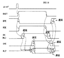
[実施の形態1]
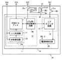
図1は、この発明が適用される半導体装置の全体の構成を概略的に示す図である。図1において、この発明に従う半導体装置10は、1トランジスタ/1キャパシタ型のダイナミック型メモリセルを含むDRAMマクロ11と、このDRAMマクロ11とデータの授受を行なうロジック回路12を含む。これらのDRAMマクロ11およびロジック回路12は、同一半導体チップ上に集積化される。
[Embodiment 1]
FIG. 1 schematically shows an entire configuration of a semiconductor device to which the present invention is applied. Referring to FIG. 1, a
DRAMマクロ11は、ダイナミック型メモリセルを有するDRAMセルアレイ13と、基本的にこのDRAMセルアレイ13に含まれるメモリセルの選択およびデータの書込/読出を行なうためのDRAM周辺回路14を含む。
The
ロジック回路12は、このDRAMマクロ11からのデータを読出して所定の処理を行ないかつ処理後のデータをDRAMマクロ11のメモリセルへ書込むコアロジック回路15を含む。ロジック回路12と外部との信号を授受する周辺回路部は、この半導体装置10のチップ上に、延在して配置される(ピン端子が、この半導体装置10のチップ4辺に沿って配置される)が、ここではロジック回路の中心機能を実現するコアロジック回路15を代表的に示す。
The
DRAM周辺回路14はCMOS回路で構成され、またコアロジック回路15も、CMOS回路で構成される。これらのDRAM周辺回路14およびコアロジック回路15は、しきい値電圧およびゲート絶縁膜膜厚が同じMOSトランジスタを基本的に使用する。
The DRAM
この半導体装置10において、比較的長い期間にわたって処理が行なわれないとき、コアロジック回路15はスリープモードに入り、クロック信号の発生を停止させ、内部回路動作を停止する。コアロジック回路15は、スリープモードに入ると、DRAMマクロ11をセルフリフレッシュモードに設定する。DRAMマクロ11は、セルフリフレッシュモードに入ると、内蔵のタイマを利用して、所定の時間間隔で、メモリセルデータのリフレッシュを実行する。
In the
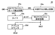
図2は、この発明の実施の形態1に従う半導体装置の要部の構成をより詳細に示す図である。図2において、DRAMマクロ11は、セルフリフレッシュモードが指定されたときDRAMセルアレイ13のメモリセルのデータのリフレッシュを行なうためのリフレッシュ系回路14aと、DRAMセルアレイ13のメモリセルの列選択、データの書込/読出およびノーマルモード時の動作制御を行なうコラム系/周辺制御回路14bを含む。このコラム系/周辺制御回路14bおよびリフレッシュ系回路14aは、図1に示すDRAM周辺回路14に含まれる。セルフリフレッシュモード時においては、コラム系周辺制御回路14bは、リフレッシュ系回路14aの制御の下に動作が停止される。
FIG. 2 shows in more detail the structure of the main part of the semiconductor device according to the first embodiment of the present invention. In FIG. 2, a
リフレッシュ系回路14aは、セルフリフレッシュモード時、セルフリフレッシュ動作に必要な制御動作を行なうセルフリフレッシュ制御回路(SR制御回路)20と、セルフリフレッシュモード時、SR制御回路20の制御の下にDRAMセルアレイ13のメモリセル行の選択および選択行のメモリセルデータの読出/再書込(リストア)を行なうロウ系回路21を含む。このロウ系回路21は、通常動作モード時においては、コラム系/周辺制御回路14bに含まれる周辺制御回路の制御の下に、DRAMセルアレイ13の行選択に関連する動作を行なう。SR制御回路20は、セルフリフレッシュモード検出回路、リフレッシュアドレスを発生するリフレッシュアドレスカウンタ、セルフリフレッシュ期間をカウントするタイマおよびリフレッシュアドレスカウンタからのリフレッシュアドレスを外部からのロウアドレスに代えてロウ系回路21へ与えるマルチプレクサを含む。
The
ロウ系回路21は、ロウアドレスおよびリフレッシュアドレスをデコードするロウデコーダ、ロウデコーダの出力信号に従ってDRAMセルアレイ13のワード線を選択状態へ駆動するワード線ドライブ回路、およびDRAMセルアレイ13の各列に設けられ、各列上のメモリセルデータの検知および増幅を行なうセンスアンプ回路、各列(ビット線対)のプリチャージ/イコライズを行なうビット線プリチャージ/イコライズ回路を含む。
Row-related
この半導体装置10は、さらに、外部からの電源電圧EV1を受け、内部電源電圧VC1を生成してロジック回路12に対する動作電源電圧を与える電源回路22aと、外部電源電圧EV2を受けて内部電源電圧VC2を生成してコラム系/周辺制御回路14bに対する動作電源電圧を与える電源回路22bと、外部電源電圧EV3を受けて内部電源電圧VC3およびVC4を生成して、DRAMセルアレイ13およびリフレッシュ系回路14aへ与える電源回路22cと、ロジック回路12に含まれるコアロジック回路15の制御の下に、電源回路22aおよび22bに対する電源制御信号φ1およびφ2を生成する電源制御回路25を含む。この電源制御回路25は、ロジック回路12がスリープモードに入り、DRAMマクロがセルフリフレッシュモードに設定されるとき、電源回路22aおよび22bの内部電源電圧VC1およびVC2発生動作を停止させる。
The
ここで、電源回路22cから内部電源電圧VC3がDRAMセルアレイ13へ与えられているのは、この内部電源電圧VC3は、DRAMセルアレイ13におけるビット線プリチャージ/イコライズ電圧およびメモリセルのセルプレート電圧を発生するために利用されており、またロウ系回路21に含まれるセンスアンプ回路においてこの内部電源電圧VC3が利用されることを示すためである。内部電源電圧VC4は、ロウ系回路21に含まれるワード線ドライブ回路およびロウデコーダおよびSR制御回路20へ与えられる。
Here, the internal power supply voltage VC3 is applied to the
この図2に示す構成において、電源回路22a−22cは、外部電源電圧EV1、EV2およびEV3をそれぞれ受けて、内部電源電圧VC1〜VC3を生成している。しかしながら、これらの電源回路22a−22cは、以下に詳細に説明するように、それぞれ接地電圧をも発生する。以下、単に電源電圧と称すときには、ハイレベル電源電圧Vccを示し、「電源供給電圧」と称すときには、電源電圧および接地電圧両者を参照するものとする。
In the configuration shown in FIG. 2,
電源制御回路25は、常時、電源供給電圧を受けて動作する。この電源制御回路25は、電源回路22aおよび22bに共通に設けられるように示すが、電源制御回路25は、電源回路22aおよび22bそれぞれに対応して別々に設けられてもよい。また、電源回路22aがロジック回路12内に設けられ、また電源回路22bおよび22cは、DRAMマクロ11内に設けられてもよい。
The power
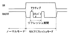
この発明の実施の形態1においては、電源回路22aおよび22bは、セルフリフレッシュモード時その内部電源供給電圧発生動作を停止させる。一方通常モード(ノーマルモード)においては、電源回路22a、22bおよび22cをすべて動作させる。半導体装置の動作モードは、DRAMマクロ11およびロジック回路15が動作する通常モード(ノーマルモード)時と、スリープモードと呼ばれる低消費電流スタンバイ状態がある。通常モード時においては、DRAMマクロ11の状態としては、実際にメモリセルの選択およびアクセスが行なわれるアクティブサイクルおよび次のアクセスを待つスタンバイサイクルが存在する。スリープモード時においては、DRAMマクロ11はセルフリフレッシュモードに設定される。このセルフリフレッシュモード時においても、DRAMマクロ11は、内部に設けられるタイマの出力信号に従ってリフレッシュサイクルが形成されてリフレッシュ動作が実行される。
In the first embodiment of the present invention,
通常モード時においては、ロジック回路15およびDRAMマクロ11は、内部スタンバイサイクル時であっても、数十mAの電流消費は許容される。一方、スリープモード時においては、消費電流は、DRAMマクロ11のデータ保持を行なうための電流であり、できるだけ小さくする必要がある。リフレッシュサイクル時においては、DRAMマクロの内部でのリフレッシュ動作が行なわれるだけであり、このDRAMマクロへのアクセスは行なわれないため、アクセス時間およびサイクル時間の遅延は何ら問題は生じない。したがって、図2に示すように、セルフリフレッシュ動作に関連するリフレッシュ系回路14aに対する電源回路22cのみをセルフリフレッシュモード時動作させ、電源回路22aおよび22bからの内部電源供給電圧発生動作は停止させ、消費電流を低減する。
In the normal mode, the
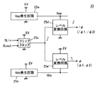
図3は、図2に示すコラム系/周辺制御回路14bに対する電源回路22bの構成を示す図である。この電源回路22bは、外部電源電圧EV2を伝達する主電源線1と、接地電圧Vssを伝達する主接地線2と、主電源線1に対応して設けられるサブ電源線3と、主接地線2に対応して設けられるサブ接地線4と、制御信号/φ2に応答して導通し、主電源線1およびサブ電源線3を接続するPチャネルMOSトランジスタPQ1と、制御信号φ2の活性化に応答して導通し、主接地線2をサブ接地線4に接続するNチャネルMOSトランジスタNQ1を含む。
FIG. 3 shows a configuration of
コラム系/周辺制御回路14bは、その内部構成は、実現する機能により異なるが、図3においては、5段のインバータIV1−IV5を一例として示す。これらのインバータIV1−IV5は、CMOS構成であり、PチャネルMOSトランジスタPTおよびNチャネルMOSトランジスタNTを含む。コラム系/周辺制御回路14bは、ロジック回路12に含まれるMOSトランジスタと同じ(ゲート絶縁膜およびしきい値電圧について)であり、低しきい値電圧(L−Vth)MOSトランジスタで構成される。
Although the column system /
リークカット用のMOSトランジスタPQ1およびNQ1は、この低しきい値電圧MOSトランジスタPTおよびNTのしきい値電圧の絶対値よりも大きな絶対値のしきい値電圧を有するMOSトランジスタ(M−VthMOSトランジスタ)で構成される。制御信号φ2および/φ2は、図2に示す電源制御回路25から与えられ、通常モード(ノーマルモード)およびセルフリフレッシュモードでその論理レベルが切換えられる。
Leakage cut MOS transistors PQ1 and NQ1 are MOS transistors (M-VthMOS transistors) having a threshold voltage having an absolute value larger than the absolute value of the threshold voltage of low threshold voltage MOS transistors PT and NT. Consists of. Control signals .phi.2 and /.phi.2 are applied from power
コラム系/周辺制御回路14bは、DRAMマクロ11がダイナミック動作を行なっており、スタンバイ状態時において、入力信号INの論理レベルは予め知ることができる。この入力信号INのスタンバイ状態時における論理レベルに応じて、内部回路のインバータIV1−IV5の電源供給ノードの接続先が決定される。図3においては、インバータIV1、IV3およびIV5が主電源線1とサブ接地線4に結合され、インバータIV2およびIV4がサブ電源線3と主接地線2に結合される。この状態においては、入力信号INはスタンバイ状態においては、Lレベルに設定される。次に、この図3に示す電源回路22bの動作を、図4に示す信号波形図を参照して説明する。
In the column /
DRAMマクロへのアクセスを行なうノーマルモード時(スタンバイサイクルおよびアクティブサイクルを含む)においては、制御信号φ2がHレベルおよび制御信号/φ2がLレベルに設定され、リークカット用MOSトランジスタPQ1およびNQ1がともにオン状態に設定される。この状態においては、主電源線1上の電源電圧EV2がサブ電源線3上に伝達され、また主接地線2上の接地電圧Vssがサブ接地線4上に伝達される。したがって、この状態においては、サブ電源線3上の電源電圧SVcc(VC2)およびサブ接地線4上の電源電圧SVssはそれぞれ外部電源電圧EV2および接地電圧Vssと等しく、コラム系/周辺制御回路14bは、その低しきい値電圧MOSトランジスタにより高速で動作する。
In a normal mode (including a standby cycle and an active cycle) for accessing the DRAM macro, control signal φ2 is set to H level and control signal / φ2 is set to L level, and leakage cut MOS transistors PQ1 and NQ1 are both set. Set to the on state. In this state, power supply voltage EV2 on main
ノーマルモード時におけるスタンバイサイクル時において、入力信号INの論理レベルがLレベルに固定されても、制御信号φ2および/φ2はともにそれぞれ、HレベルおよびLレベルに設定され、主電源線1はサブ電源線3に接続され、またサブ接地線4は主接地線2に接続される。通常モード時においては、スタンバイサイクル時でも、数十mAの電流消費は許容されているため、このスタンバイサイクル時において、コラム系/周辺制御回路14bおよびリフレッシュ系回路14aにおいて電流が消費されても、許容範囲内であり、問題は生じない。これは、ロジック回路12においても同様である。
In the standby cycle in the normal mode, even if the logic level of input signal IN is fixed at L level, control signals φ2 and / φ2 are both set to H level and L level, respectively, and main
ロジック回路12は、所定時間以上処理を行なわない場合、スリープモードに入り、DRAMマクロ11は、セルフリフレッシュモードに設定される。この状態において、電源制御回路25からの制御信号φ2および/φ2がそれぞれLレベルおよびHレベルに設定され、リークカット用MOSトランジスタPQ1およびNQ1がオフ状態となる。これにより、サブ電源線3およびサブ接地線4がハイインピーダンス状態となり、コラム系/周辺制御回路14bにおける消費電流は、リークカット用MOSトランジスタPQ1およびNQ1のリーク電流により決定される値となり、低消費電流モードが実現される。特に、リークカット用MOSトランジスタPQ1およびNQ1のしきい値電圧の絶対値は、このコラム系/周辺制御回路14bに含まれるMOSトランジスタのしきい値電圧よりも絶対値が大きいため、これらのリークカット用MOSトランジスタPQ1およびNQ1は、深いオフ状態となり、リーク電流を確実に抑制する。
When the
セルフリフレッシュモードからノーマルモードに移行すると、制御信号φ2および/φ2がそれぞれHレベルおよびLレベルに変化する。サブ電源線3およびサブ接地線4上の電圧SVcc(VC2)およびSVssが、所定の電圧レベルに復帰するまでにある時間が必要である。しかしながら、セルフリフレッシュモードからノーマルモードに移行する場合、セルフリフレッシュサイクルを確実に完了させて内部回路が確実にスタンバイ状態にあることを保証する必要がある。このため、セルフリフレッシュモードからノーマルモードへの移行時、またはスリープモードからノーマルモードへの移行時、実際の回路動作は、ある所定の時間経過後に行なうように仕様で定められている。したがって、セルフリフレッシュモードからノーマルモードへの移行時、サブ電源線3およびサブ接地線4上の電源電圧の元の電圧レベルへの復帰までに時間を要しても、何らその間、回路動作は実行されないため、問題は生じない。
When shifting from the self-refresh mode to the normal mode, control signals φ2 and / φ2 change to H level and L level, respectively. A certain time is required until voltages SVcc (VC2) and SVss on sub
セルフリフレッシュモードにおいては、この図2に示す電源回路22cは常時内部電源電圧VC3およびVC4を発生しており(動作電流をも供給する)、リフレッシュ系回路14aが動作し、所定の周期でDRAMセルアレイ13内のメモリセルのリフレッシュを実行する。したがって、アクセス動作に何ら悪影響を及ぼすことなく消費電流を低減することができる。
In the self-refresh mode, the
図5は、図2に示すロジック回路用電源回路22aの構成を示す図である。図5において、電源回路22aは、外部電源電圧EV1を伝達する主電源線1aと、主電源線1aに対応して設けられるサブ電源線3aと、制御信号/φ1がLレベルのとき導通して、主電源線1aとサブ電源線3aとを接続するリークカット用PチャネルMOSトランジスタPQaと、接地電圧Vssを伝達する主接地線2aと、主接地線2aに対応して設けられるサブ接地線4aと、制御信号φ1がHレベルのとき導通して、主接地線2aとサブ接地線4aを接続するNチャネルMOSトランジスタNQaを含む。これらのリークカット用MOSトランジスタPQaおよびNQaは、そのしきい値電圧の絶対値は比較的大きくされる(ロジック回路の構成要素のMOSトランジスタに比べて)。
FIG. 5 is a diagram showing a configuration of the logic circuit
ロジック回路12は、その実現する論理により、その内部構成は異なるが、図5においては、5段のインバータIVa−IVeを示す。これらのインバータIVa−IVeは、それぞれ、CMOSインバータであり、低しきい値電圧MOSトランジスタPTおよびNTを含む。これらのインバータIVa−IVeは、サブ電源線3a上の電圧SVcc(VC1)およびサブ接地線4a上の電圧SVsSを両動作電源電圧として動作する。
Although the internal configuration of the
ロジック回路12は、所定の論理処理を行なっており、この入力信号INの電圧レベルを予測することができない。したがって、このサブ電源線3aおよびサブ接地線4a上の電圧SVccおよびSVssを利用することにより、スリープモード時の消費電流を、入力信号INの電圧レベルにかかわらず低減する。次に、この図5に示す電源回路22aの動作を図6に示す信号波形図を参照して説明する。
The
ノーマルモード時においては、制御信号/φ1およびφ1がそれぞれLレベルおよびHレベルに設定され、リークカット用MOSトランジスタPQaおよびNQaはオン状態となり、低インピーダンスで主電源線1aおよび主接地線2aをそれぞれ、サブ電源線3aおよびサブ接地線4aに接続する。この状態においては、ロジック回路12は、その低しきい値電圧MOSトランジスタにより、高速で動作し、所定の論理処理を実行する。
In the normal mode, control signals / φ1 and φ1 are set to L level and H level, respectively, leak-cut MOS transistors PQa and NQa are turned on, and main power supply line 1a and
スリープモードが設定されると、制御信号/φ1がHレベル、制御信号φ1がLレベルとなり、リークカット用MOSトランジスタPQaおよびNQaはオフ状態となり、これらのサブ電源線3aおよびサブ接地線4aはハイインピーダンスで主電源線1aおよび主接地線2aにそれぞれ接続される。リークカット用MOSトランジスタPQaおよびNQaのリーク電流は小さいため、ロジック回路12におけるスリープモード時の消費電流を低減することができる。特に、ロジック回路12においては、スリープモード時、保持データのリフレッシュ動作は何ら実行されないため、その消費電流は単なるリーク電流のみである。
When the sleep mode is set, control signal / φ1 is at H level and control signal φ1 is at L level, leakage cut MOS transistors PQa and NQa are turned off, and sub
スリープモードからノーマルモードに移行すると、制御信号φ1および/φ1はそれぞれHレベルおよびLレベルに駆動され、サブ電源線3aおよびサブ接地線4aがそれぞれ主電源線1aおよび主接地線2aに低インピーダンスで接続される。これらのサブ電源線3a上の電圧SVcc(VC1)およびサブ接地線4a上の電圧SVssが、所定の電圧レベルに復帰するまでに時間が必要とされる(サブ電源線3aおよびサブ接地線4aの寄生容量の充放電のため)。しかしながら、スリープモードからノーマルモードに移行時、このロジック回路の動作開始は、スリープモード解除後ある時間が経過してからのみ許容される。したがって、この場合においても、サブ電源線3aおよびサブ接地線4a上の電圧SVccおよびSVssの復帰に時間を要しても、何らロジック回路12の動作開始タイミングが遅れることはなく、何ら問題は生じず、高速動作性能は低下しない。
When shifting from the sleep mode to the normal mode, the control signals φ1 and / φ1 are driven to the H level and the L level, respectively, and the sub
なお、図5に示す構成においては、ロジック回路12は、スリープモード時、内部信号INの論理レベルが予め予測できないとして説明している。しかしながら、このロジック回路12が、スリープモードが設定された場合、内部状態を初期状態にリセットし、各内部信号の状態が予め予測することができる場合には、図3に示すように、内部信号(入力信号)INの論理レベルに応じて、各回路(インバータ)の電源ノードと電源供給線との接続が決定されればよい(図3に示す電源構成と同様の構成)。
In the configuration shown in FIG. 5, the
図7は、ロジック回路12の電源回路の他の構成を示す図である。この図7に示す構成においては、ロジック回路12は、外部からの電源電圧EV1をその電源ノードに受ける。外部電源電圧EV1は、ノーマルモード時においては、所定の電圧レベルに設定され、一方スリープモード時には、電源供給が遮断される(外部のプロセサの制御の下に)。したがって、ロジック回路12は、スリープモード時この外部電源電圧EV1供給が遮断されるため、内部回路の電流消費経路は存在せず、その消費電流を、0とすることができる。この図7に示す構成においては、電源回路は特に設けられない(単なる電源線のみであり、制御信号φ1は使用されない)。
FIG. 7 is a diagram illustrating another configuration of the power supply circuit of the
リフレッシュ系回路に対する電源回路22cは、常時リフレッシュ系回路およびDRAMセルアレイに電源電圧VC3およびVC4を伝達する。したがって、この電源回路は、必要な電圧(ビット線プリチャージ電圧およびセルプレート電圧)を発生する回路および必要ならば内部降圧回路を、電源供給電圧を伝達する電源線で構成され、ノーマルモード時およびスリープモード時、内部電源電圧VC3およびVC4を発生する。
The
このリフレッシュ系回路に対する電源回路22cは、階層電源構成を有していてもよい(ただしリークカット用MOSトランジスタはセルフリフレッシュモード時のリフレッシュサイクル時オン状態)。
The
なお、上述の説明において、サブ電源線3aおよび3bの電圧SVccは、スリープモード時およびセルフリフレッシュモード時、電源電圧よりも少し低下した電圧レベルに設定されている。しかしながら、このサブ電源線の放電により、サブ電源線3aおよび3bの電圧レベルが、接地電圧レベルにまで低下するように構成されてもよい。
In the above description, voltage SVcc of sub
[変更例1]
図8は、この発明の実施の形態1の変更例1の構成を示す図である。この図8においては、コラム系/周辺制御回路14bに対する電源回路22bの構成を示す。図8に示す電源回路22bは、リークカット用MOSトランジスタとして、低しきい値電圧(L−Vth)のMOSトランジスタPQbおよびNQbが用いられる。PチャネルMOSトランジスタPQbは、主電源線1bとサブ電源線3bの間に接続され、NチャネルMOSトランジスタNQbが、主接地線2bとサブ接地線4bの間に接続される。リークカット用MOSトランジスタPQbおよびNQbは、コラム系/周辺制御回路14bのMOSトランジスタPTおよびNTと同一のしきい値電圧(L−Vth)を有する。リークカット用MOSトランジスタPQbおよびNQbのゲートへ与えられる制御信号/φ2およびφ2は、上で説明した実施例と同じであり、セルフリフレッシュモード時に非活性化され、リークカット用MOSトランジスタPQbおよびNQbをオフ状態に設定する。
[Modification 1]
FIG. 8 is a diagram showing a configuration of a first modification of the first embodiment of the present invention. FIG. 8 shows a configuration of
これらのリークカット用MOSトランジスタPQbおよびNQbのオフ状態時に流れるオフリーク電流Ioffは、サブ電源線3bおよびサブ接地線4bを流れるリーク電流の総和Ioff(14b)よりも小さくなるように、そのゲート幅が調整される。コラム系/周辺制御回路14bにおけるサブ電源線3bを流れるオフリーク電流は、PチャネルMOSトランジスタPQbのオフリーク電流に等しく、コラム系/周辺制御回路14bがMOSトランジスタPQbのオフリーク電流よりも大きなオフリーク電流を生じさせるとき、サブ電源線3bの電圧SVccの電圧レベルが低下し、コラム系/周辺制御回路14bのMOSトランジスタPTのゲート−ソース間がより強い逆バイアス状態となり、オフリーク電流が低減され、結果的に、このMOSトランジスタPQbのオフリーク電流により回路のリーク電流が決定される。これは、リークカット用のNチャネルMOSトランジスタNQbについても同様である。
The gate width of the off-leakage current Ioff flowing when these leak-cut MOS transistors PQb and NQb are off is smaller than the total Ioff (14b) of the leakage currents flowing through the sub
通常モードにおいては、リークカット用MOSトランジスタPQbおよびNQbがともにオン状態となる。この場合、図8に示すコラム系/周辺制御回路14bにおいてインバータIV1−IV5は、すべて同時に充放電するのではなく、ある一定の遅延時間をもって動作しており、したがって、このMOSトランジスタPQbおよびNQbのオフリーク電流を低減するためにゲート幅が小さくされても、通常モード時における回路動作に何ら悪影響は及ぼさない。
In the normal mode, leak cut MOS transistors PQb and NQb are both turned on. In this case, in the column-related /
図9は、ロジック回路12に対する電源回路22aの構成を示す図である。この図9に示す電源回路22aにおいては、制御信号/φ1のLレベルのとき導通し、外部電源電圧EV1をロジック回路12へ動作電源電圧として伝達するPチャネルMOSトランジスタPQcと、制御信号φ1がHレベルのとき導通し、接地電圧Vssをロジック回路12の他方動作電源電圧として、供給するNチャネルMOSトランジスタNQcを含む。ロジック回路12は、低しきい値電圧(L−Vth)のMOSトランジスタを構成要素として含んでおり、これらのリークカット用MOSトランジスタPQcおよびNQcも、ロジック回路12に含まれるMOSトランジスタと同様低しきい値電圧(L−Vth)MOSトランジスタである。
FIG. 9 is a diagram illustrating a configuration of the
この図9に示す構成において、これらのMOSトランジスタPQcおよびNQcのオフリーク電流は、ロジック回路12におけるオフリーク電流の総和よりも小さくされる。したがって、この図9に示す電源回路22aの構成においても、スリープモード時、ロジック回路12の動作が停止されるとき、そのオフリーク電流が、リークカット用MOSトランジスタPQcおよびNQcにより決定され、スリープモード時のオフリーク電流を低減でき、低消費電流を実現することができる。
In the configuration shown in FIG. 9, the off leak currents of these MOS transistors PQc and NQc are made smaller than the sum of the off leak currents in
通常モード時においては、これらのリークカット用MOSトランジスタPQcおよびNQcはオン状態となり、ロジック回路12に対し安定に動作電流を供給する。
In the normal mode, these leak-cutting MOS transistors PQc and NQc are turned on to supply an operating current to the
なお、ロジック回路12も、このスリープモード時、内部回路ノードが初期状態にセットされ、その各内部回路のノードのスリープモード時の電圧レベルが編め確定することができる場合には、図8に示す構成と同じ電源回路を利用することができる。
When the
[変更例2]
図10は、この発明の実施の形態1の変更例2の構成を示す図である。この図10においては、コラム系/周辺回路に対する電源回路22bの構成を示す。この電源回路22bにおいて、主電源線1bとサブ電源線3bの間に、リークカット用のPチャネルMOSトランジスタPQdが接続され、主接地線2bとサブ接地線4bの間にリークカット用のNチャネルMOSトランジスタNQdが設けられる。これらのリークカット用のMOSトランジスタPQdおよびNQdは、低しきい値電圧(L−Vth)MOSトランジスタであってもよく、それより大きなしきい値電圧の絶対値を有する中間しきい値電圧(M−Vth)MOSトランジスタであってもよい。リークカット用MOSトランジスタPQdのゲートへ与えられる制御信号/φ2は、接地電圧Vssと外部電源電圧EV2よりも高い昇圧電圧Vppとの間で変化する。また、リークカット用NチャネルMOSトランジスタNQdのゲートへ与えられる制御信号φ2は、電源電圧Vccおよび接地電圧Vssよりも低い負電圧Vbbの間で変化する。電源電圧Vccは、外部電源電圧EV2の電圧レベルと等しくてもよい。
[Modification 2]
FIG. 10 is a diagram showing a configuration of a second modification of the first embodiment of the present invention. FIG. 10 shows a configuration of
セルフリフレッシュモード時においては、制御信号/φ2が昇圧電圧Vppのレベルに設定され、また制御信号φ2が負電圧Vbbの電圧レベルに設定される。したがって、リークカット用MOSトランジスタPQdおよびNQdは、ゲート−ソース間が深い逆バイアス状態に設定され、より深いオフ状態となり、オフリーク電流をより低減することができる。 In the self-refresh mode, control signal / φ2 is set to the level of boosted voltage Vpp, and control signal φ2 is set to the voltage level of negative voltage Vbb. Therefore, leak-cut MOS transistors PQd and NQd are set in a deep reverse bias state between the gate and the source, become deeper in an off state, and can further reduce off-leakage current.
通常モード時においては、制御信号/φ2は接地電圧Vssレベルに設定され、制御信号φ2は電源電圧Vcc(または外部電源電圧EV2)の電圧レベルに設定される。したがって、通常モード時においては、サブ電源線3bおよびサブ接地線4bは、低インピーダンスで主電源線1bおよび主接地線2bに接続され、コラム系/周辺制御回路14bは高速で動作する。
In the normal mode, control signal / φ2 is set to the level of ground voltage Vss, and control signal φ2 is set to the voltage level of power supply voltage Vcc (or external power supply voltage EV2). Therefore, in the normal mode, sub
なお、ロジック回路に対する電源回路22aについても、この図10に示す構成と同様の構成または図9に示す構成と同様の構成が利用されればよい。制御信号φ1および/φ1の振幅を大きくすることにより、スリープモード時リークカット用MOSトランジスタをより深いオフ状態に設定する。
As for the
図11は、この変更例2における電源制御回路25の構成を概略的に示す図である。図11において、電源制御回路25は、外部電源電圧EV(EV1,EV2)を受けて外部電源電圧EVよりも高い昇圧電圧Vppを発生するVpp発生回路25aと、外部電源電圧EVを受け、接地電圧Vssよりも低い負電圧Vbbを発生するVbb発生回路25bと、ロジック回路からのスリープモード開始指示信号SLinに従ってセットされかつスリープモード終了指示信号SLoutに従ってリセットされるフリップフロップ25cと、フリップフロップ25cの出力信号をレベル変換して制御信号/φ(/φ1,/φ2)を出力するレベル変換回路25dと、フリップフロップ25cの出力信号のレベル変換を行なって制御信号φ(φ1,φ2)を生成するレベル変換回路25eを含む。
FIG. 11 is a diagram schematically showing the configuration of the power
フリップフロップ25cは外部電源電圧EVを一方動作電源電圧として動作する。レベル変換回路25dは、このフリップフロップ25cの出力信号がHレベルとなると、そのHレベルを昇圧電圧Vppレベルに変換して出力する。レベル変換回路25eは、フリップフロップ25cからの出力信号のHレベルを負電圧Vbbレベルに変換して制御信号φを生成する。制御信号/φのLレベルは接地電圧Vssレベルであり、制御信号φのHレベルは外部電源電圧EVレベルである。
The flip-
この図11に示す電源制御回路25において、DRAMマクロに対する電源回路に対する制御信号φ2,/φ2を発生する部分と、ロジック回路の電源回路に対する制御信号/φ1およびφ1を発生する回路が別々に設けられ、それぞれの外部電源電圧のレベルが調整されてもよい。
In power
また、電源制御回路25が、DRAMマクロおよびロジック回路に対し別々に設けられる場合、DRAMマクロに対して設けられる電源制御回路は、DRAMマクロ内において用いられるワード線昇圧用の高電圧Vppおよびアレイ基板領域をバイアスするためのバックゲートバイアスVbbを利用するように構成されてもよい。次に、この図11に示す電源制御回路25の動作を図12に示す信号波形図を参照して説明する。
When power
スリープモードに入ると、スリープモード開始指示信号SLinがワンショットパルスの形で与えられ、フリップフロップ25cがセットされ、その出力信号がHレベルとなる。応じてレベル変換回路25dからの制御信号/φ(/φ1,/φ2)が外部電源電圧EVよりも高い昇圧電圧Vppレベルに駆動される。一方、レベル変換回路25eはこのフリップフロップ25cの出力信号の立上がりに応答して制御信号φを負電圧Vbbレベルに駆動する。
When the sleep mode is entered, the sleep mode start instruction signal SLin is given in the form of a one-shot pulse, the flip-
フリップフロップ25cは、外部電源電圧EVを受けており、その状態を維持する。スリープモードが完了すると、スリープモード終了指示信号SLoutがワンショットパルスの形で与えられ、フリップフロップ25cの出力信号がLレベルとなる。応じてレベル変換回路25dからの制御信号/φ(/φ1,/φ2)が接地電圧VssレベルのLレベルとなる。また、レベル変換回路25eがこのフリップフロップ25cの出力信号の立上がりに応答して制御信号φを外部電源電圧EVレベルに駆動する。
Flip-
したがって、このスリープモード時(セルフリフレッシュモード時)、リークカット用MOSトランジスタをより深いオフ状態に設定することができ、よりオフリーク電流を低減でき消費電流を低減することができる。 Therefore, in this sleep mode (in the self-refresh mode), the leak-cut MOS transistor can be set to a deeper off state, and the off-leak current can be further reduced and the current consumption can be reduced.
なお、実施の形態1において、レベル変換を行なわない場合、このフリップフロップ25cから相補な制御信号を取出すことにより、リークカット用MOSトランジスタに対する制御信号φ(φ1,φ2)および/φ(/φ1,/φ2)を生成することができる。
In the first embodiment, when level conversion is not performed, control signals φ (φ1, φ2) and / φ (/ φ1,) for the leakage cut MOS transistors are obtained by taking out complementary control signals from flip-
レベル変換回路25dおよび25eは、たとえば周知のラッチ型のCMOS変換回路で構成される。
[変更例3]
図13は、この発明の実施の形態1の変更例3の構成を概略的に示す図である。この図13に示す構成においては、主電源線1bとサブ電源線3bの間に設けられるリークカット用PチャネルMOSトランジスタPQbのバックゲート(Nウェル)へ電圧φwnが与えられ、また主接地線2bとサブ接地線4bの間に設けられるリークカット用NチャネルMOSトランジスタNQbのバックゲート(Pウェル)へウェル電圧φwpが与えられる。これらのリークカット用MOSトランジスタPQbおよびNQbは、低しきい値電圧(L−Vth)MOSトランジスタである。
[Modification 3]
FIG. 13 schematically shows a configuration of a third modification of the first embodiment of the present invention. In the configuration shown in FIG. 13, voltage φwn is applied to the back gate (N well) of leakage cut P-channel MOS transistor PQb provided between main
これらのリークカット用MOSトランジスタPQbおよびNQbのウェル電圧φwnおよびφwpを、動作モードに応じて変更する。すなわち、スリープモード(セルフリフレッシュモード)においては、リークカット用MOSトランジスタPQbのバックゲート(Nウェル)へ与えられるウェル電圧φwnを外部電源電圧EV2よりも高い昇圧電圧Vppレベルに設定し、またリークカット用NチャネルMOSトランジスタNQbのバックゲート(Pウェル)へ与えられるウェル電圧φwpを負電圧Vbbレベルに設定する。したがって、これらのリークカット用MOSトランジスタPQbおよびNQbは、バックゲートバイアスが深くなり、そのしきい値電圧の絶対値が大きくなり、リーク電流を抑制する。 Well voltages φwn and φwp of leak cutting MOS transistors PQb and NQb are changed according to the operation mode. That is, in the sleep mode (self-refresh mode), well voltage φwn applied to the back gate (N well) of leak cut MOS transistor PQb is set to boosted voltage Vpp level higher than external power supply voltage EV2, and leak cut is also performed. Well voltage φwp applied to the back gate (P well) of N channel MOS transistor NQb for use is set to negative voltage Vbb level. Therefore, these leak cut MOS transistors PQb and NQb have a deep back gate bias, an absolute value of the threshold voltage thereof, and suppress a leak current.
通常モード時においては、ウェル電圧φwnは外部電源電圧EV2の電圧レベルに設定され、ウェル電圧φwpが、接地電圧Vssレベルに設定される。したがって、通常モード時においては、これらのリークカット用MOSトランジスタPQbおよびNQbは、低しきい値電圧MOSトランジスタとして動作し、深いオン状態となって動作電流を十分に供給することができる。 In the normal mode, well voltage φwn is set to the voltage level of external power supply voltage EV2, and well voltage φwp is set to the level of ground voltage Vss. Therefore, in the normal mode, these leak-cut MOS transistors PQb and NQb operate as low threshold voltage MOS transistors and are in a deep ON state and can sufficiently supply an operating current.
図14は、この発明の実施の形態1の変更例3の電源制御回路25の構成を概略的に示す図である。図14において、電源制御回路25は、外部電源電圧EVと接地電圧Vssを受けて、この外部電源電圧EVよりも高い昇圧電圧Vppを発生するVpp発生回路25aと、外部電源電圧EVと接地電圧Vssとを受け、接地電圧Vssよりも低い負電圧Vbbを発生するVbb発生回路25bと、ロジック回路からのスリープモード開始指示信号SLinに応答してセットされかつロジック回路からのスリープモード終了指示信号SLoutに従ってリセットされて、外部電源電圧EVの振幅を有する制御信号/φおよびφを発生するフリップフロップ25cと、Vpp発生回路25aからの昇圧電圧Vppと接地電圧とを動作電源電圧として受け、フリップフロップ25cからの制御信号/φのレベルを変換して互いに相補な切換制御信号φpおよび/φpを発生するレベル変換回路25fと、外部電源電圧EVとVbb発生回路25bからの負電圧Vbbとを動作電源電圧として受け、フリップフロップ25cからの制御信号φのレベルを変換して互いに相補な切換制御信号φnおよび/φnを生成するレベル変換回路25gと、レベル変換回路25fからの切換制御信号φpおよび/φpに従って昇圧電圧Vppおよび外部電源電圧EVの一方を選択してウェル電位φwnを生成する切換回路25hと、レベル変換回路25eからの制御信号φnおよび/φnに従って接地電圧Vssおよび負電圧Vbbの一方を選択してウェル電圧φwpを生成する切換回路25iを含む。
FIG. 14 schematically shows a structure of power
レベル変換回路25fは、フリップフロップ25cからの制御信号/φがHレベルとなると、切換制御信号φpを接地電圧レベル、切換制御信号/φpを昇圧電圧Vppレベルに設定する。レベル変換回路25gは、フリップフロップ25cからの制御信号φがLレベルに立下がると、切換制御信号φnを負電圧Vbbレベルに設定し、一方、切換制御信号/φnを外部電源電圧EVレベルに設定する。
切換回路25hは、切換制御信号φp2がLレベルのとき導通し、昇圧電圧Vppを伝達するPチャネルMOSトランジスタPT1と、レベル変換回路からの切換制御信号/φpがLレベルのとき導通し、外部電源電圧EVを伝達するPチャネルMOSトランジスタPT2を含む。
切換回路25iは、レベル変換回路25eからの制御信号φnがHレベルとなると導通して接地電圧Vssを伝達するNチャネルMOSトランジスタNT1と、レベル変換回路25eからの切換制御信号/φnがHレベルとなると導通して、負電圧Vbbを伝達するNチャネルMOSトランジスタNT2を含む。次に、この図14に示す電源制御回路25の動作を、図15に示す信号波形図を参照して説明する。
Switching circuit 25i is turned on when control signal φn from
セルフリフレッシュモード(スリープモード)に入るとき、スリープモード開始指示信号SLinがワンショットパルスの形で活性化される。応じて、フリップフロップ25cからの制御信号/φが接地電圧Vssレベルから外部電源電圧EVレベルに立上がり、また制御信号φが外部電源電圧EVレベルから接地電圧Vssレベルに低下する。レベル変換回路25fは、この制御信号/φがHレベルに立上がると、切換制御信号φpを昇圧電圧Vppレベルから接地電圧Vssレベルに駆動する。また、レベル変換回路25eは、このフリップフロップ25cからの制御信号φの立下がりに応答して、切換制御信号φnを外部電源電圧EVレベルから負電圧Vbbレベルに立下げる。
When entering the self-refresh mode (sleep mode), the sleep mode start instruction signal SLin is activated in the form of a one-shot pulse. Accordingly, control signal / φ from flip-
応じて、切換回路25hにおいては、MOSトランジスタPT1がオン状態、MOSトランジスタPT2がオフ状態となり、ウェル電圧φwnとして、昇圧電圧VppがPチャネルMOSトランジスタPT1を介して伝達される。昇圧電圧Vppがウェル電圧φwnとして出力される場合においても、MOSトランジスタPT2は、そのゲートおよびソースが同一電圧であり、オフ状態を維持する。
Accordingly, in switching
また、切換回路25iにおいては、MOSトランジスタNT1がオフ状態、MOSトランジスタNT2がオン状態となり、負電圧Vbbがウェル電圧φwpとして出力される。この状態は、セルフリフレッシュモード(スリープモード)が維持されている間保持される。 In switching circuit 25i, MOS transistor NT1 is turned off, MOS transistor NT2 is turned on, and negative voltage Vbb is output as well voltage φwp. This state is maintained while the self-refresh mode (sleep mode) is maintained.
セルフリフレッシュモードすなわちスリープモードが完了すると、スリープモード終了指示信号SLoutがワンショットパルスの形でHレベルに駆動され、フリップフロップ25cからの制御信号φが外部電源電圧EVレベル、制御信号/φが接地電圧Vssレベルに変化する。応じて、レベル変換回路25fにおいては、切換制御信号φpが昇圧電圧Vppレベルとなり、補の切換制御信号/φpが接地電圧Vssレベルとなる。したがって、切換回路25hにおいては、MOSトランジスタPT1がオフ状態、MOSトランジスタPT2がオン状態となり、ウェル電圧φw2として、外部電源電圧EVがMOSトランジスタPT2を介して出力される。この状態において、MOSトランジスタPT1はソースおよびゲートが同一電圧であり、オフ状態を維持する。
When the self refresh mode, that is, the sleep mode is completed, the sleep mode end instruction signal SLout is driven to the H level in the form of a one-shot pulse, the control signal φ from the flip-
レベル変換回路25gは、制御信号φの立上がりに応答して切換制御信号φnを負電圧Vbbから外部電源電圧EVレベルに立上げ、補の切換制御信号/φnを外部電源電圧EVから負電圧Vbbレベルに立下げる。したがって、切換回路25iにおいては、MOSトランジスタNT1がオン状態、MOSトランジスタNT2がオフ状態となり、ウェル電圧φwpとして接地電圧VssがMOSトランジスタNT1を介して伝達される。このウェル電圧φwpが接地電圧レベルに設定された場合においても、MOSトランジスタNT2は、そのゲートおよびソースが同一電圧であり、オフ状態を維持する。
ノーマルモード時には、ウェル電圧φwnが外部電源電圧EVレベル、ウェル電位φwpが接地電圧Vssレベルとなり、リークカット用MOSトランジスタPQbおよびNQdを低しきい値電圧MOSトランジスタとして動作させることができる。 In the normal mode, well voltage φwn is at external power supply voltage EV level and well potential φwp is at ground voltage Vss level, and leakage cut MOS transistors PQb and NQd can be operated as low threshold voltage MOS transistors.
なお、この図14に示す電源制御回路の構成においても、DRAMマクロおよびロジック回路それぞれ別々に電源制御回路が設けられてもよい。 In the configuration of the power supply control circuit shown in FIG. 14, a power supply control circuit may be provided separately for each of the DRAM macro and the logic circuit.
また、ロジック回路において、この動作モードを制御するための信号SLinおよびSLoutを発生する回路は、外部に設けられたプロセサからの指示信号を受ける必要があり、常時動作する必要があるため、この回路部分に対しては、外部電源電圧が常時与えられる。 Further, in the logic circuit, the circuit that generates the signals SLin and SLout for controlling the operation mode needs to receive an instruction signal from a processor provided outside, and needs to operate constantly. An external power supply voltage is always applied to the portion.
なお、変更例2および3をそれぞれ組合せ、制御信号の電圧レベルのレベル変換およびウェル電圧レベルの変換をセルフリフレッシュモード時行なうように構成してもよい。 Note that modification examples 2 and 3 may be combined, and the voltage level conversion of the control signal and the well voltage level conversion may be performed in the self-refresh mode.
以上のように、この発明の実施の形態1に従えば、スリープモード時メモリセルデータのリフレッシュ動作に関連する部分に対してのみ電源供給電圧を供給し、他の回路部分に対しては、電源供給電圧の供給停止(動作電流の供給停止)を行なうように構成しているため、アクセス時間の増大をもたらすことなくスタンバイ状態時における消費電流を低減することができる。 As described above, according to the first embodiment of the present invention, the power supply voltage is supplied only to the portion related to the refresh operation of the memory cell data in the sleep mode, and the power is supplied to the other circuit portions. Since the supply voltage supply is stopped (operation current supply is stopped), current consumption in the standby state can be reduced without increasing the access time.
[実施の形態2]
図16は、この発明の実施の形態2に従う半導体装置の全体の構成を概略的に示す図である。この図16に示す半導体装置においては、半導体装置10は、LSIチップ30上に形成される。DRAMマクロ11を取囲むようにロジック回路12が形成される。LSIチップ30上のロジック回路12外部に、ロジック回路12に対する電源トランジスタ31aおよびDRAMマクロ11のコラム系/周辺制御回路14bに対する電源トランジスタ31bが設けられる。これらの電源トランジスタ31aおよび31bは、PチャネルMOSトランジスタで構成され、電源制御回路25からのセルフリフレッシュモード(スリープモード)指示信号SR1およびSR2に従って選択的にオン状態となり、それぞれ外部電源電圧EV1およびEV2をロジック回路12およびコラム系/周辺制御回路14bへ供給する。
[Embodiment 2]
FIG. 16 schematically shows a whole structure of the semiconductor device according to the second embodiment of the present invention. In the semiconductor device shown in FIG. 16,
DRAMセルアレイ13へは外部電源電圧EV3が常時、与えられ、リフレッシュ系回路14aには、常時、外部電源電圧EV4が与えられる。これらの外部電源電圧EV1−EV4は、それぞれの電源電圧レベルが互いに異なってもよく、いくつかの外部電源電圧が同じ電圧レベルであってもよい。
External power supply voltage EV3 is always applied to
図17は、ロジック回路12およびコラム系/周辺制御回路14bの電源構成を概略的に示す図である。図17においては、これらのロジック回路12およびコラム系/周辺制御回路14bを内部回路33で表わす。内部回路33に対する電源線32は、電源トランジスタ31を介して外部電源電圧EVを受ける。この内部回路33の他方電源供給ノードは接地ノードであり、接地電圧Vssを受ける。次に、この図16および図17に示す装置の動作を図18に示す信号波形図を参照して説明する。
FIG. 17 schematically shows a power supply configuration of
ロジック回路12が動作し、かつDRAMマクロ11へロジック回路12がアクセスする通常動作モード時においては、セルフリフレッシュモード(スリープモード)指示信号SR(SR1およびSR2)はLレベルであり、電源トランジスタ31aおよび31bはオン状態にある。この状態においては、ロジック回路12には外部電源電圧EV1が与えられ、またコラム系/周辺制御回路14bへは、外部電源電圧EV2が与えられる。DRAMセルアレイ13およびリフレッシュ系回路14aには、それぞれ外部電源電圧EV3およびEV4が供給される。したがって、この半導体装置内の構成要素を低しきい値電圧MOSトランジスタで構成することにより、高速動作が実現される。
In the normal operation mode in which the
セルフリフレッシュモード(スリープモード)時においては、セルフリフレッシュモード(スリープモード)指示信号SR(SR1,SR2)が外部電源電圧レベルのHレベルとなり、電源トランジスタ31aおよび31bがオフ状態となる。この状態においては、ロジック回路12およびコラム系/周辺制御回路14bへの電源電圧の供給が停止され、これらへ与えられる動作電源電圧Vccの電圧レベルは、接地電圧レベルに低下する。したがって、この状態においては、ロジック回路12およびコラム系/周辺制御回路14bにおいては、電流消費はほとんど生じない。
In the self-refresh mode (sleep mode), self-refresh mode (sleep mode) instruction signal SR (SR1, SR2) is at the H level of the external power supply voltage level, and
一方、リフレッシュ系回路14aおよびDRAMセルアレイ13においては、このセルフリフレッシュモード時においては、所定の時間間隔でリフレッシュ動作が実行されるだけであり、その消費電流は少ない。セルフリフレッシュモード(スリープモード)から通常動作モードへの移行時において、ロジック回路12およびコラム系/周辺制御回路14bに対する動作電源電圧Vccの電圧レベルが回復するまでに、ある時間が必要とされる。しかしながら、セルフリフレッシュモード(スリープモード)から通常動作モード時移行時においては、セルフリフレッシュモード(ノーマルモード)完了後半導体装置の内部動作開始するまで、ある時間をおくことが定められている(仕様値)。したがって、何らこれらのロジック回路12およびコラム系/周辺制御回路14bの電源電圧Vccの回復にある時間を要しても、何ら高速動作性に悪影響を及ぼすことはない。
On the other hand, in
なお、この図16に示す構成において、電源トランジスタ31aおよび31bを設ける代わりに、外部のプロセサなどの制御の下に、外部電源電圧EV1およびEV2自体の供給が停止されるように構成されてもよい。
In the configuration shown in FIG. 16, instead of providing
なお、外部電源電圧EV3は、たとえば、2.5Vであり、昇圧電圧Vppおよび負電圧Vbbを生成するために使用されまたセンスアンプの電源電圧としても利用される。外部電源電圧EV1、EV2およびEV4は、たとえば1.5Vである。ロジック回路12において、その信号入出力部においては、2.5Vの電圧が動作電源電圧として印加される。なお、この図16に示す構成においては、ロジック回路12に対するこの2つの電源電圧を1つの外部電源電圧EV1で表わす。
External power supply voltage EV3 is 2.5 V, for example, and is used to generate boosted voltage Vpp and negative voltage Vbb, and is also used as a power supply voltage for the sense amplifier. External power supply voltages EV1, EV2 and EV4 are, for example, 1.5V. In the
[変更例1]
図19は、この発明の実施の形態2の変更例1の構成を概略的に示す図である。この図19に示す構成においては、DRAMセルアレイ13およびリフレッシュ系回路14aに対し、電源制御回路35からの活性化制御信号RACTに応答してその状態(インピーダンス)が切換えられる電源回路36が設けられる。他の構成は、図16に示す構成と同じである。
[Modification 1]
FIG. 19 schematically shows a configuration of a first modification of the second embodiment of the present invention. In the configuration shown in FIG. 19, a
電源制御回路35は、SR制御回路20の制御の下に、セルフリフレッシュモード時、実際にリフレッシュ動作が行なわれるとき、制御信号RACT0をHレベルの活性状態に駆動する。電源回路36は、この活性制御信号RACT0がHレベルとなると、低インピーダンス状態となる。通常動作モード時においては、この電源回路36は、低インピーダンス状態を維持する。
Under the control of
図20は、図19に示す電源回路36の構成を概略的に示す図である。図20において、電源回路36は、制御信号ZRACT0がLレベルのとき導通し、主電源線1dとサブ電源線3dとを接続するPチャネルMOSトランジスタPQdと、制御信号RACTがHレベルのとき導通し、主接地線2dをサブ接地線4dに接続するNチャネルMOSトランジスタNQdを含む。
FIG. 20 schematically shows a configuration of
リフレッシュ系回路14aは、スタンバイ状態時における入力信号INの論理に応じて電源ノードの接続先が定められる。図20においても、このリフレッシュ系回路14aとして、5段のインバータIV1−IV5を代表的に示す。リークカット用MOSトランジスタPQdおよびNQdのしきい値電圧は、L−VthMOSトランジスタPTおよびNTに比べて比較的高くされる。次に、この図19および20に示す構成の動作を図21に示す信号波形図を参照して説明する。
In the
通常動作モード時においては、制御信号RACT0はHレベル、制御信号ZRACT0はLレベルである。リークカット用MOSトランジスタPQdおよびNQdはともにオン状態にあり、サブ電源線3dおよびサブ接地線4dはそれぞれ主電源線1dおよび主接地線2eに接続される。この状態においては、リフレッシュ系回路14aは、電源が低インピーダンス状態にあり、高速動作する。
In the normal operation mode, control signal RACT0 is at H level and control signal ZRACT0 is at L level. Leakage cut MOS transistors PQd and NQd are both on, and sub
セルフリフレッシュモードに入ると、制御信号RACT0がLレベル、制御信号ZRACT0がHレベルとなる。このセルフリフレッシュモード時においては、SR制御回路20の制御の下に所定の周期でリフレッシュ動作が実行される。このリフレッシュ動作時、制御信号RACT0がHレベル制御信号ZRACT0がHレベルとなり、リークカット用MOSトランジスタPQdおよびNQdがともにオン状態となる。したがって、リフレッシュ動作時においては、安定に電流が供給されて、リフレッシュ動作を行なうことができる。リフレッシュ周期でアクティブサイクルおよびスタンバイサイクルがリフレッシュ系回路14aにおいて実行され、そのアクティブサイクル時においては、電源回路36のインピーダンスが低くされる。これにより、スタンバイ状態時における消費電流をより低減することができる。コラム系/周辺制御回路14bおよびロジック回路12の電源回路は、先の図16に示す構成の場合と同様である。
When the self-refresh mode is entered, the control signal RACT0 becomes L level and the control signal ZRACT0 becomes H level. In the self-refresh mode, a refresh operation is executed at a predetermined cycle under the control of the
図22は、図19に示す電源制御回路35の構成の一例を示す図である。図22において、電源制御回路35は、セルフリフレッシュモード指示信号SRを受けるインバータ35aとインバータ35aの出力信号とアレイ活性化指示信号ACTを受けて制御信号RACT0を生成するOR回路35bを含む。セルフリフレッシュモード指示信号SRは、セルフリフレッシュモード時Hレベルとなる。アレイ活性化指示信号ACTは、ロウ系回路21が動作状態の間Hレベルとなる。したがって、この制御信号RACT0は通常動作モード時、常時、Hレベルとなり、セルフリフレッシュモード時、アレイ活性化信号ACTに従ってHレベルとなる。
FIG. 22 is a diagram showing an example of the configuration of power
なお、図19に示す構成においては、SR制御回路20およびロウ系回路21に対する電源がともに制御されている。しかしながら、SR制御回路20においては、リフレッシュ周期を決定するタイマを含んでおり、このタイマの動作を安定化するため、SR制御回路20へは常時電源電圧を印加し、ロウ系回路21に対してのみ図20に示すような階層電源構成が利用されてもよい。
In the configuration shown in FIG. 19, both the power supply to the
[変更例2]
図23は、この発明の実施の形態2の変更例2の構成を概略的に示す図である。この図23に示す構成においては、コラム系/周辺制御回路14bに対し、外部電源電圧EV2を降圧する内部降圧回路が設けられる。すなわち、コラム系/周辺制御回路14bに対する電源回路として、内部電源電圧と所定電圧とを比較する比較器39と、比較器39の出力信号に従って外部電源電圧EV2を受ける電源ノードからコラム系/周辺制御回路14bへの電源線に電流を供給するPチャネルMOSトランジスタ31cと、セルフリフレッシュモード(スリープモード)指示信号SR2がLレベルのとき導通し、基準電圧Vrefを選択して所定電圧として比較器39へ与えるPチャネルMOSトランジスタ37と、セルフリフレッシュモード(スリープモード)指示信号SR2がHレベルのとき導通し接地電圧Vssを所定電圧として比較器39へ伝達するNチャネルMOSトランジスタ38を含む。他の構成は、図16に示す構成と同じである。
[Modification 2]
FIG. 23 schematically shows a configuration of a second modification of the second embodiment of the present invention. In the configuration shown in FIG. 23, an internal step-down circuit for stepping down external power supply voltage EV2 is provided for column-related /
この図23に示す構成においては、通常動作モード時において、セルフリフレッシュモード(スリープモード)指示信号SR(SR1,SR2)がLレベルであり、NチャネルMOSトランジスタ38がオフ状態、PチャネルMOSトランジスタ37がオン状態となり、基準電圧Vrefが比較器39へ与えられる。したがって、比較器39およびPチャネルMOSトランジスタ31cのフィードバックループが、基準電圧Vrefとほぼ実質的に電圧レベルが等しくなる内部電源電圧を生成してコラム系/周辺制御回路14bへ与える。
In the configuration shown in FIG. 23, in the normal operation mode, self refresh mode (sleep mode) instruction signal SR (SR1, SR2) is at L level, N
一方、セルフリフレッシュ(スリープ)モード時においては、MOSトランジスタ37がオフ状態、MOSトランジスタ38がオン状態となり、接地電圧が比較器39へ与えられる。したがって、比較器39は、接地電圧レベルにコラム系/周辺制御回路14bの内部電源電圧を設定する。なお、この比較器39は外部電源電圧EV2に従って動作する。
On the other hand, in the self-refresh (sleep) mode,
また図23に示す構成においては、電源制御回路25が、ロジック回路12に対する電源電圧およびコラム系/周辺制御回路14bに対する内部降圧回路の動作制御を行なう信号SR2およびSR1を生成してる。しかしながら、このコラム系/周辺制御回路14bに対する内部降圧回路の動作制御用の信号SR2を発生する回路とロジック回路12に対する電源トランジスタの動作を制御する信号SR1を発生する電源制御回路はそれぞれ別々に設けられてもよい。
In the configuration shown in FIG. 23, power
コラム系/周辺制御回路14bにおいては、セルフリフレッシュモード時においては、接地電圧レベルに内部電源電圧が設定されるため、電流消費は生じない。単に比較器39の比較動作により、電流が消費されるだけである。基準電圧Vrefは、外部電源電圧EV2から生成されるが、この基準電圧発生回路は、大きな電流駆動能力が要求されないため、その消費電流は十分小さい。
In column /
以上のように、この発明の実施の形態2に従えば、セルフリフレッシュモード(スリープモード)時においては、回路動作を停止する部分への電源供給を遮断するように構成しているため、セルフリフレッシュモード(スリープモード)時における消費電流を大幅に低減することができる。また、通常動作モード時には、常時外部からの電源電圧が供給されるため、低しきい値電圧MOSトランジスタにより高速動作が実現される。 As described above, according to the second embodiment of the present invention, in the self-refresh mode (sleep mode), the power supply to the portion where the circuit operation is stopped is cut off. Current consumption in the mode (sleep mode) can be greatly reduced. In the normal operation mode, since the power supply voltage is always supplied from the outside, high speed operation is realized by the low threshold voltage MOS transistor.
[実施の形態3]
図24は、この発明の実施の形態3の半導体装置の構成を概略的に示す図である。図24においては、ロジック回路12に対し基板バイアス電圧を発生するウェル電位発生回路51aが設けられ、またDRAMマクロ11のコラム系/周辺制御回路14bに対し基板バイアス電圧を発生するウェル電位発生回路51bが設けられる。これらのウェル電位発生回路51aおよび51bは対応の回路の基本領域へバイアス電圧を印加し、ウェル電位制御回路55からのウェル電位制御信号SR1,SR2およびZSR1,ZSR2によりその発生電位が切換えられる。
[Embodiment 3]
FIG. 24 schematically shows a structure of a semiconductor device according to the third embodiment of the present invention. 24, a well
DRAMセルアレイ13およびリフレッシュ系回路14aのNウェル領域へは、常時、外部電源電圧EV3およびEV4がそれぞれNウェル電圧として供給される。Pウェル領域には、図示しない接地電圧がまたこれらのDRAMセルアレイ13およびリフレッシュ系回路14bに与えられる。ここで、DRAMセルアレイ13のPウェル(基板領域)へ、負電圧Vbbが基板バイアス電圧として与えられてもよい。
External power supply voltages EV3 and EV4 are always supplied as N well voltages to
図25は、図24に示すウェル電位発生回路51aおよび51bの構成を概略的に示す図である。これらのウェル電位発生回路51aおよび51bは、同じ回路構成を有するため、図25において1つのウェル電位発生回路51を代表的に示す。
FIG. 25 schematically shows structures of well
図25においては、PチャネルMOSトランジスタが形成されるNウェル(基板領域)に印加される電圧VSNを発生する部分の構成を示す。図25において、ウェル電位発生回路51は、外部電源電圧EVから、この外部電源電圧EVよりも高い昇圧電圧Vppを発生するVpp発生回路57と、制御信号SRPがLレベルのとき導通し、外部電源電圧EVを通過させるPチャネルMOSトランジスタ56aと、制御信号ZSRPがLレベルのとき導通し、Vpp発生回路57からの昇圧電圧Vppを通過させるPチャネルMOSトランジスタ56bを含む。これらのMOSトランジスタ56aおよび56bからの電圧がウェル電圧VSNとして対応の回路に形成されたPチャネルMOSトランジスタのウェル領域(基板領域)へ与えられる。制御信号SRPは、外部電源電圧EVと接地電圧Vssの電圧レベルの間で変化し、制御信号ZSRPは、接地電圧Vssと昇圧電圧Vppの間で変化する。
FIG. 25 shows a configuration of a portion for generating voltage VSN applied to an N well (substrate region) where a P-channel MOS transistor is formed. In FIG. 25, well
図26は、図24に示すウェル電位発生回路51の、対応の回路内のNチャネルMOSトランジスタが形成されるPウェル(基板領域)へ印加されるウェル電位VSPを発生する部分の構成を概略的に示す図である。図26において、ウェル電位発生回路51は、外部電源電圧EVから負電圧Vbbを発生するVbb発生回路58と、制御信号ZSRNがHレベルのとき導通し、接地電圧Vssを通過させるPチャネルMOSトランジスタ56cと、制御信号SRNがHレベルのとき導通し、Vbb発生回路58からの負電圧Vbbを通過させるNチャネルMOSトランジスタ56dを含む。これらのMOSトランジスタ56cおよび56dから与えられる電圧VSPが、基板バイアス電圧として対応の回路内のNチャネルMOSトランジスタが形成されるPウェル(基板領域)へ与えられる。制御信号SRNおよびZSRNは、電源電圧EVと負電圧Vbbの間で変化する。
FIG. 26 schematically shows a configuration of a portion of well
セルフリフレッシュモード時においては、制御信号ZSRPが接地電圧Vssレベル、制御信号SRPが昇圧電圧Vppレベルとなり、MOSトランジスタ56bがオン状態、MOSトランジスタ56aがオフ状態となり、Nウェルへ、昇圧電圧Vppが印加される。したがって、PチャネルMOSトランジスタのしきい値電圧の絶対値が大きくなり、リーク電流が抑制される。
In the self-refresh mode, control signal ZSRP is at ground voltage Vss level, control signal SRP is at boosted voltage Vpp level,
また図26に示すように、セルフリフレッシュモード時において、制御信号SRNが外部電源電圧EVレベル、制御信号ZSRNが負電圧Vbbレベルとなり、MOSトランジスタ56dがオン状態、MOSトランジスタ56cがオフ状態となり、Pウェル電位VSPは、負電圧Vbbレベルとなる。したがって、セルフリフレッシュモード時NチャネルMOSトランジスタの基板バイアスが深くなり、そのしきい値電圧が大きくなり、リーク電流が低減される。
As shown in FIG. 26, in the self-refresh mode, the control signal SRN is at the external power supply voltage EV level, the control signal ZSRN is at the negative voltage Vbb level, the
通常動作モード時においては制御信号SRPが接地電圧Vssレベル、制御信号ZSRPが昇圧電圧Vppレベルとなり、MOSトランジスタ56aがオン状態、MOSトランジスタ56bがオフ状態となり、Nウェルの電位VSNは外部電源電圧EVレベルとなる。
In the normal operation mode, the control signal SRP is at the ground voltage Vss level, the control signal ZSRP is at the boost voltage Vpp level, the
同様、図26において、制御信号SRNが負電圧Vbbレベル、制御信号ZSRNが外部電源電圧EVレベルとなり、MOSトランジスタ56dがオフ状態、MOSトランジスタ56cがオン状態となり、Pウェル電位VSPは、接地電圧Vssレベルとなる。これにより、低しきい値電圧MOSトランジスタが実現され高速動作が実現される。
Similarly, in FIG. 26, the control signal SRN is at the negative voltage Vbb level, the control signal ZSRN is at the external power supply voltage EV level, the
なお、この図25から図26に示すウェル電位発生回路51に対し制御信号を発生する部分の構成は、図14に示す構成を利用することができる。また、電源回路も同様セルフリフレッシュモード(スリープモード)と通常モード(ノーマルモード)において電源のオン/オフまたはインピーダンスの調整が実行される(実施の形態1または2を利用)。なお、外部電源電圧をセルフリフレッシュモード(スリープモード)時に遮断する場合、特に、このウェル電位を制御する必要はない(リーク経路は存在しないため)。
The configuration shown in FIG. 14 can be used as the configuration for generating the control signal for well
以上のように、この発明の実施の形態3に従えば、セルフリフレッシュモード(スリープモード)時において、回路動作が停止される回路部分のウェル(基板領域)電位の絶対値を大きくしているため、回路内の構成要素の低しきい値電圧のMOSトランジスタのしきい値電圧の絶対値を大きくすることができ、オフリーク電流を低減することができ、消費電流を低減することができる。 As described above, according to the third embodiment of the present invention, in the self-refresh mode (sleep mode), the absolute value of the well (substrate region) potential of the circuit portion where the circuit operation is stopped is increased. The absolute value of the threshold voltage of the low threshold voltage MOS transistor of the component in the circuit can be increased, the off-leakage current can be reduced, and the current consumption can be reduced.
[実施の形態4]
図27は、この発明の実施の形態4に従う半導体装置の全体の構成を概略的に示す図である。図27に示す構成においては、DRAMセルアレイ13へは外部電源電圧EV3が与えられ、またリフレッシュ系回路14aには、外部電源電圧EV4が与えられる。ロジック回路12へは、制御信号SR1に応答する電源トランジスタ31aを介して外部電源電圧EV1が動作電源電圧として与えられる。コラム系/周辺制御回路14bへは、制御信号SR2に応答する電源トランジスタ31bを介して外部電源電圧EV2が動作電源電圧として与えられる。
[Embodiment 4]
FIG. 27 schematically shows a whole structure of the semiconductor device according to the fourth embodiment of the invention. In the configuration shown in FIG. 27, external power supply voltage EV3 is applied to
DRAMマクロ11においては、さらに、このリフレッシュ系回路14aおよびDRAMセルアレイ13のウェル電圧(基板領域の電圧)VsubrおよびVsubmの電圧レベルを制御するウェル電源回路60が設けられる。他の構成は、図6に示す構成と同じであり、対応する部分には同一参照番号を付す。また電源制御回路25が、制御信号SR1およびSR2をともに生成しているが、この電源制御回路25は、電源トランジスタ31aおよび31bそれぞれに対応して別々に設けられてもよい。
In
ウェル電源回路60の具体的構成は、たとえば図14に示す構成と同じであり、リフレッシュ系回路14aに含まれるSR制御回路20からのセルフリフレッシュモード指示信号SRに従って各回路基板領域へ印加されるウェル電圧VsubrおよびVsubmの絶対値を大きくする。図14の回路においてウェル電圧φwnおよびφwpをそれぞれNウェル電位VSNおよびPウェル電位VSPに変更することにより、この図27に示すウェル電源回路60の構成が実現される。DRAMセルアレイ13およびリフレッシュ系回路14aそれぞれのウェル電圧VsubrおよびVsubmの絶対値は、それぞれの回路特性に応じて適当な値に設定される。
The specific configuration of well
[変更例]
図28は、図27に示すウェル電源回路60の変更例の構成を示す図である。この図28に示すウェル電源回路は、DRAMセルアレイ13のたとえばメモリセルが形成されるPウェルの電圧VSPを調整する。
[Example of change]
FIG. 28 shows a configuration of a modified example of well
図28において、DRAMセルアレイ13に対するウェル電源回路60は、外部電源電圧EV3に従って昇圧電圧Vppを発生するVpp発生回路60aと、外部電源電圧EV3を一方動作電源電圧として受けて動作し、接地電圧よりも低い負電圧Vbb1を発生するVbb1発生回路60bと、外部電源電圧EV3を動作電源電圧として受けて動作し、負電圧Vbb1よりも絶対値の小さな負電圧Vbb2を発生するVbb2発生回路60cと、昇圧電圧Vppおよび接地電圧Vssを両動作電源電圧として受けて動作し、セルフリフレッシュモード指示信号SR3の電圧レベルを変換して制御信号φpおよび/φpを生成するレベル変換回路60dと、外部電源電圧EV3と負電圧Vbb1を両動作電源電圧として動作し、セルフリフレッシュモード指示信号SR3のレベルを変換して切換制御信号φnおよび/φnを生成するレベル変換回路60eと、レベル変換回路60dからの切換制御信号φpおよび/φpに従って外部電源電圧EV3および昇圧電圧Vppの一方を選択してNウェルへ印加されるNウェル電圧VSNを生成する切換回路60fと、レベル変換回路60eからの切換制御信号φnおよび/φnに従って負電圧Vbb1およびVbb2の一方を選択してPウェルへ印加されるPウェル電圧VSPを生成する切換回路60gを含む。
In FIG. 28, well
切換回路60fは、切換制御信号φpがLレベルのとき導通し、昇圧電圧Vppを伝達するPチャネルMOSトランジスタPT3と、切換制御信号/φpがLレベルのとき導通し外部電源電圧EV3を伝達するPチャネルMOSトランジスタPT4を含む。MOSトランジスタPT3およびPT4の一方により、Nウェル電圧VSNが生成される。
切換回路60gは、切換制御信号φnがHレベルのとき導通し、負電圧Vbb2を伝達するNチャネルMOSトランジスタNT3と、切換制御信号/φnがHレベルのとき導通し、負電圧Vbb1を伝達するNチャネルMOSトランジスタNT4を含む。これらのMOSトランジスタNT3およびNT4が伝達する電圧がPウェル電圧VSPとなる。
なお、Vpp発生回路60a、Vbb1発生回路60bおよびVbb2発生回路60cは、それぞれキャパシタのチャージポンプ動作を利用する回路により所望電圧を生成する。次に、この図28に示す回路の動作を図29に示す信号波形図を参照して説明する。
セルフリフレッシュモード時において、セルフリフレッシュモード指示信号SR3がHレベルとなり、切換制御信号φpがLレベル、切換制御信号/φpがHレベルとなる。したがって、切換回路60fにおいてMOSトランジスタPT3がオン状態、MOSトランジスタPT4がオフ状態となり、Nウェル電圧VSNは昇圧電圧Vppレベルとなる。一方レベル変換回路60eは、このセルフリフレッシュモード指示信号SR3の立上がりに応答して切換制御信号φnを負電圧Vbb1レベルのLレベル、切換制御信号φnを外部電源電圧EV3のHレベルに設定する。したがって、切換回路60gにおいては、MOSトランジスタNT3がオフ状態、MOSトランジスタNT4がオン状態となり、Pウェル電圧VSPとして負電圧Vbb1が伝達される。MOSトランジスタNT3はゲート電圧が負電圧Vbb1レベルであり、そのソース電位がPウェル電圧VSPと同じ電圧レベルであり、オフ状態を維持する。
In the self-refresh mode, self-refresh mode instruction signal SR3 is at H level, switching control signal φp is at L level, and switching control signal / φp is at H level. Therefore, in switching
通常動作モード時(ノーマルモード時)においては、セルフリフレッシュモード指示信号SR3がLレベルとなり、切換制御信号φpが昇圧電圧VppレベルのHレベル、切換制御信号/φpが接地電圧レベルのLレベルとなり、Nウェル電圧VSNは、切換回路60fのオン状態のMOSトランジスタPT4により外部電源電圧EV3の電圧レベルになる。
In the normal operation mode (in normal mode), self-refresh mode instruction signal SR3 is at L level, switching control signal φp is at H level of boosted voltage Vpp level, and switching control signal / φp is at L level of ground voltage level, N well voltage VSN is set to the voltage level of external power supply voltage EV3 by MOS transistor PT4 in the on state of switching
一方、レベル変換回路60eは切換制御信号φnを外部電源電圧EV3のHレベル、切換制御信号/φnを負電圧Vbb1レベルのLレベルに設定する。したがって、切換回路60gにおいて、MOSトランジスタNT3がオン状態、MOSトランジスタNT4がオフ状態となり、Pウェル電圧VSPとして、負電圧Vbb2が伝達される。したがって、セルフリフレッシュモード時、Nウェル電圧VSNおよびPウェル電圧VSPは、通常動作モード時よりもその絶対値が大きくされており、より深いバイアス状態となり、アレイおよび回路内のMOSトランジスタのオフリーク電流を低減する。
On the other hand,
[リフレッシュ系回路の構成]
図30は、図27に示すリフレッシュ系回路の構成を概略的に示す図である。セルフリフレッシュモード時においては通常動作モード時とウェル電位が異なることにより、MOSトランジスタのしきい値電圧およびドレイン電流が変化し、応じて回路性能が変化する。したがって、通常動作モード時と同じタイミングでロウ系回路を動作させた場合、メモリセルデータのリフレッシュを正確に行なうことができなくなることが考えられる。このウェル電位変化を補正する機能を、図30および図31に示すリフレッシュ系回路は備える。
[Configuration of refresh circuit]
FIG. 30 schematically shows a structure of the refresh circuit shown in FIG. In the self-refresh mode, the well potential is different from that in the normal operation mode, so that the threshold voltage and drain current of the MOS transistor change, and the circuit performance changes accordingly. Therefore, when the row circuit is operated at the same timing as in the normal operation mode, it is considered that the refresh of the memory cell data cannot be performed accurately. The refresh circuit shown in FIGS. 30 and 31 has a function of correcting the well potential change.
図30においては、リフレッシュ系回路14aに含まれるSR制御回路20の構成を概略的に示す。図30において、SR制御回路20は、外部から与えられる動作モード指示信号(コマンド)CMDに従ってセルフリフレッシュモードが指定されたことを検出するセルフリフレッシュモード検出回路20aと、セルフリフレッシュモード検出回路20aからのセルフリフレッシュモード検出信号に応答して起動され、所定の時間間隔でリフレッシュ要求信号φrefを発生するタイマ20bと、タイマ20bからのリフレッシュ要求信号φrefに従って所定の時間幅を有するワンショットのアレイ活性化信号RACT(ACT)を発生するセルフリフレッシュ設定回路20cと、セルフリフレッシュモード時起動され、このセルフリフレッシュ設定回路20cからのアレイ活性化信号RACT(ACT)の非活性化に応答して、そのカウント値を1増分してリフレッシュ行を示すリフレッシュアドレスRFADを出力するアドレスカウンタ20dと、セルフリフレッシュモード検出回路20aからのセルフリフレッシュモード検出信号に応答して、外部からのアクセス動作(列選択動作)を禁止する外部アクセス禁止回路20eを含む。
FIG. 30 schematically shows a configuration of the
この図30に示すSR制御回路20へは、図27に示す外部電源電圧EV4が常時与えられ、また構成要素のMOSトランジスタのウェル電圧が図27に示すウェル電源回路60の制御の下に制御される。したがって、セルフリフレッシュモード時において、MOSトランジスタのしきい値電圧の絶対値が変化した場合、タイマ20bの出力するリフレッシュ要求信号φREFの周期およびセルフリフレッシュ設定回路20cからのアレイ活性化信号RACT(図22の信号ACTに対応)の活性化期間が変化する。しかしながら、このセルフリフレッシュモード時に設定されるウェル電位に応じて予めタイマ20bおよびセルフリフレッシュ設定回路20cの動作パラメータを設定することにより、所定の周期でセルフリフレッシュ要求信号φrefを生成し、かつ一定のたとえば700nsの時間幅を有するアレイ活性化信号RACTを発生することができる。この図30に示すSR制御回路20は、セルフリフレッシュモードが設定されたときに動作し、通常動作モード時には動作しないため、通常動作モード時におけるアクセス動作に何ら影響は及ぼさない。
The
図31は、図27に示すロウ系回路21の構成を概略的に示す図である。図31において、ロウ系回路21は、セルフリフレッシュモード時、図30に示すセルフリフレッシュ設定回路20cからのアレイ活性化信号RACTの活性化に応答してロウデコーダ活性化信号RDEを発生するロウデコーダ活性化回路21aと、ロウデコーダ活性化回路21aからのロウデコーダ活性化信号RDEの活性化に応答して所定期間経過後ワード線ドライブ信号MRXを発生するワード線ドライブ活性化回路21bと、ワード線ドライブ活性化回路21bからのワード線ドライブ信号MRXの活性化に応答して所定期間経過後センスアンプ活性化信号MSAEを活性化するセンスアンプ活性化回路21cと、セルフリフレッシュモード指示信号SR3によりその遅延時間が変更され、ワード線ドライブ活性化回路21bからのワード線ドライブ信号MRXを設定された時間遅延してワード線ドライブ信号RXを生成する可変遅延回路21eと、セルフリフレッシュモード指示信号SR3によりその遅延時間が調整され、センスアンプ活性化回路21cからのセンスアンプ活性化信号MSAEに従ってセンスアンプ活性化信号SAEを生成する可変遅延回路21fと、可変遅延回路21fからのセンスアンプ活性化信号SAEの非活性化に応答してビット線プリチャージ/イコライズ指示信号BPEを活性化するビット線プリチャージ/イコライズ活性化回路21dを含む。
FIG. 31 schematically shows a structure of row-related
これらのワード線ドライブ活性化回路21b、センスアンプ活性化回路21cおよびプリチャージ/イコライズ活性化回路21dはアレイ活性化信号RACTの非活性化に応答してそれぞれ所定のタイミングで対応の信号MRX、MSAE、およびBPEを非活性化する。
These word line
可変遅延回路21eおよび21fは、セルフリフレッシュモード指示信号SR3が活性状態にありセルフリフレッシュモード時には、その遅延時間を長くし、通常動作モード時には、その遅延時間は短くされる。
ロウ系回路21は、さらに、ロウデコーダ活性化回路21aからのロウデコーダ活性化信号RDEの活性化に応答して活性化され、図30に示すアドレスカウンタ20dからのリフレッシュアドレスRFADをデコードするロウデコーダ21gと、ロウデコーダ21gからのデコード信号と可変遅延回路21eからのワード線ドライブ信号RXとに従ってアドレス指定された行に対応するワード線WLを選択状態へ駆動するワード線ドライバ21hと、DRAMセルアレイ13の各列(ビット線対)BLPにそれぞれ対応して設けられ、ビット線プリチャージ/イコライズ指示信号BPEに従ってビット線対BLPの電位を所定の電圧レベルにプリチャージしかつイコライズするビット線プリチャージ/イコライズ回路21jと、センスアンプ活性化信号SAEの活性化時活性化され、DRAMセルアレイ13のビット線対BLPへの電位を差動増幅するセンスアンプ回路21iを含む。
Row-related
このDRAMセルアレイ13に対して設けられるセンスアンプ回路21iは図27に示す外部電源電圧EV3を動作電源電圧として消費し、ビット線プリチャージ/イコライズ回路21jは、このDRAMセルアレイ13に与えられる外部電源電圧EV3から生成される中間電圧レベルに、ビット線対BLPをプリチャージしかつイコライズする。この図31に示す残りのロウ系回路要素は、図27に示す外部電源電圧EV4を動作電源電圧として受けて動作する。
次に、この図30および図31に示すリフレッシュ系回路14aの動作を図32に示す信号波形図を参照して説明する。
Next, the operation of
セルフリフレッシュモード時においては、セルフリフレッシュモード指示信号SR3がHレベルの活性状態となる。このセルフリフレッシュモード指示信号SR3は、図30に示すセルフリフレッシュモード検出回路20aにより生成される。外部アクセス禁止回路20eは、このセルフリフレッシュモード指示信号SR3の活性化時、外部アクセス(外部からのアクセスコマンドの受付)を禁止する。
In the self-refresh mode, self-refresh mode instruction signal SR3 is activated to an H level. Self refresh mode instruction signal SR3 is generated by self refresh
このセルフリフレッシュモード時において、所定の時間が経過すると、所定の周期でタイマ20bがリフレッシュ要求信号φrefを発生する。セルフリフレッシュ設定回路20cは、リフレッシュ要求信号φrefが発生(活性化)されると、所定の時間幅を有するワンショットのパルス信号をアレイ活性化信号RACTとして出力する。
In the self-refresh mode, when a predetermined time elapses, the
このアレイ活性化信号RACTの活性化に従って、図31に示すロウデコーダ活性化回路21aがロウデコーダ活性化信号RDEを活性化する。ロウデコーダ21gへは、図30に示すアドレスカウンタ20dからのリフレッシュアドレスRAFDが図示しないマルチプレクサを介して与えられており、ロウデコーダ21gがこのリフレッシュアドレスRFADをデコードする。このデコード動作と並行して、プリチャージ/イコライズ活性化回路21dは、ビット線プリチャージ/イコライズ指示信号BPEを非活性状態のLレベルとし、図31に示すビット線プリチャージ/イコライズ回路21jがビット線対のプリチャージ/イコライズ動作を停止する。ロウデコーダ活性化信号RDEが活性化されると、所定時間経過後、ワード線ドライブ活性化回路21bからのワード線ドライブ信号MRXが活性状態へ駆動される。可変遅延回路21eは、セルフリフレッシュモード時、その遅延時間が長くされており、ワード線ドライブ活性化回路21bからのワード線ドライブ信号MRXを所定時間遅延してワード線ドライブ信号RXを活性状態へ駆動する。したがって、ロウデコーダ21gは、MOSトランジスタのしきい値電圧の絶対値が大きくなったため、そのデコード時間が長くなった場合においても、確実に、ワード線ドライバ21hに対し、ワード線ドライブ信号RXを与え、ロウデコーダ21gからのデコード信号が確定状態となった後にワード線の活性化を行なうことができる。
In accordance with the activation of array activation signal RACT, row
ワード線ドライブ信号RXの活性化に従って選択ワード線WLの電圧レベルが上昇すると、ビット線対BLPにメモリセルMCのデータが読出される。図32においては、Hレベルデータがビット線対BLPに読出されたときのビット線対BLPの信号波形を示す。セルフリフレッシュモード時、メモリセルの基板領域も、そのバイアスが深くされており、メモリセルトランジスタのしきい値電圧は大きくなっている。したがって、セルフリフレッシュモード時、ビット線対BLPに現われる電位変化は通常動作モード時よりもゆるやかである。しかしながら、センスアンプ活性化回路21cが、センスアンプ活性化信号MSAEを活性化しても、可変遅延回路21fがセンスアンプ活性化信号FAEの活性化タイミングを遅らせている(図32において矢印で示す)。したがって、ビット線対BLPの電位が十分に拡大した後に、センスアンプ回路21iが活性化されてセンス動作を行なう。これにより、メモリセルデータのリフレッシュが確実に実行される。
When the voltage level of selected word line WL rises according to activation of word line drive signal RX, data in memory cell MC is read to bit line pair BLP. FIG. 32 shows a signal waveform of bit line pair BLP when H level data is read out to bit line pair BLP. In the self-refresh mode, the bias of the memory cell substrate region is also deepened, and the threshold voltage of the memory cell transistor is increased. Therefore, the potential change appearing on the bit line pair BLP in the self-refresh mode is more gradual than in the normal operation mode. However, even if the sense
所定時間が経過すると、図30に示すセルフリフレッシュ設定回路20cからのアレイ活性化信号RACTが非活性状態へ駆動される。このアレイ活性化信号RACTの非活性化に応答してアドレスカウンタ20dが、そのリフレッシュアドレスRFADのアドレス値を1増分する。この非活性化に応答してロウデコーダ活性化回路21aからのロウデコーダ活性化信号RDEが非活性状態へ駆動され、ロウデコーダ21gが非活性状態となり、デコード動作を完了する。このデコード動作完了時においても、ロウデコーダ21gの内部ノードのプリチャージ時間が遅れることが考えられる(セルフリフレッシュモード時)。しかしながら、この場合においても、可変遅延回路21eからのワード線ドライブ信号RXは、その非活性化が遅らされており、ロウデコーダ21gの非活性化に従って選択ワード線を個別に非選択状態へ駆動することができる。
When a predetermined time elapses, array activation signal RACT from self-
また、センスアンプ活性化信号SAEも、この可変遅延回路21fにより、ワード線WL(ワード線ドライブ信号RX)が非活性状態となった後に非活性化され、センス動作を完了する。このセンス動作が完了した後、センスアンプ活性化信号SAEの非活性化に応答して図31に示すプリチャージ/イコライズ活性化回路21dがビット線プリチャージ/イコライズ指示信号BPEを活性状態へ駆動する。したがって、この状態においてセンスアンプ回路の動作が遅い場合においても、確実に、センスアンプ回路のセンス動作が完了した後に、ビット線対BLPのプリチャージ/イコライズ動作を行なうことができる。
The sense amplifier activation signal SAE is also deactivated by the
なお、図32において信号波形内において右向き矢印で示すのは、信号が可変遅延回路21eおよび21fによりその変化タイミングが遅れることを示す。
In FIG. 32, the arrow pointing to the right in the signal waveform indicates that the change timing of the signal is delayed by the
図33は、図31に示す可変遅延回路21eおよび21fの構成の一例を示す図である。可変遅延回路21eおよび21fは同じ構成を有し、その遅延時間が異なるだけであり、図33においては、センスアンプ活性化信号SAEに対して設けられた可変遅延回路21fを示す。図33において、可変遅延回路21fは、センスアンプ活性化回路21cからのセンスアンプ活性化信号MSAEを所定時間遅延する遅延回路61aと、セルフリフレッシュモード指示信号SR3の活性化時導通し、遅延回路61aの出力信号を通過させるCMOSトランスミッションゲート61bと、セルフリフレッシュモード指示信号SR3の非活性化時導通し、センスアンプ活性化回路21cからのセンスアンプ活性化信号MSAEを通過させるCMOSトランスミッションゲート61cを含む。
FIG. 33 shows an example of the configuration of
これらのCMOSトランスミッションゲート61bおよび61cから、センスアンプ回路へ与えられるセンスアンプ活性化信号SAEが出力される。遅延回路61aは、たとえば偶数段のインバータで構成され、その遅延時間は予め定められる。
Sense amplifier activation signal SAE applied to the sense amplifier circuit is output from these
この図33に示す可変遅延回路21fと同様の構成を、図31に示す可変遅延回路21eが有している(実際の遅延時間が異なる)。したがって、セルフリフレッシュモード時、ウェル電位の絶対値を高くして、MOSトランジスタのしきい値電圧の絶対値が高くされた場合において、リフレッシュ系回路の動作速度が低下する場合においても、リフレッシュを行なうためのタイミング信号の活性化タイミングを遅延させることにより、この回路動作速度低下を抑制し、正確にリフレッシュを行なうことができる。
The
通常動作モード時においては、センスアンプ活性化信号SAEは、センスアンプ活性化回路21cからのセンスアンプ活性化信号MSAEに従って生成される。このときは、遅延は存在しないため、ウェル電位の絶対値が小さくされた場合、高速で動作することができ、通常動作モード時に、悪影響を及ぼすことはない。この通常モード時には、ロウデコーダ活性化回路21aへ、アレイ活性化信号RACTに代えて、外部信号に従ってアレイ活性化信号(ACT)が生成されて与えられる。
In the normal operation mode, sense amplifier activation signal SAE is generated according to sense amplifier activation signal MSAE from sense
以上のように、この発明の実施の形態4に従えば、セルフリフレッシュモード時、リフレッシュに関連する部分に対してのみ電源電圧を供給し、他回路に対しては電源をオフ状態とし、かつリフレッシュ動作に関連する回路部分のウェル電位の絶対値を大きくしているため、スタンバイ状態時における消費電流をより低減することができる。 As described above, according to the fourth embodiment of the present invention, in the self-refresh mode, the power supply voltage is supplied only to the portion related to the refresh, the power is turned off to the other circuits, and the refresh is performed. Since the absolute value of the well potential of the circuit portion related to the operation is increased, current consumption in the standby state can be further reduced.
[実施の形態5]
図34は、この発明の実施の形態5に従う半導体装置の構成を概略的に示す図である。図34においては、DRAMマクロ11に含まれるSR制御回路20およびコラム系/周辺制御回路14bの部分の構成を示す。
[Embodiment 5]
FIG. 34 schematically shows a structure of the semiconductor device according to the fifth embodiment of the present invention. FIG. 34 shows the configuration of the
図34において、SR制御回路20は、動作モード指示信号(コマンド)CMDに従ってセルフリフレッシュモードが指定されたことを検出するセルフリフレッシュモード検出回路20aと、このセルフリフレッシュモード検出回路20aからのセルフリフレッシュモード指示信号SRに従って計時動作を行ない、所定期間ごとにリフレッシュ要求信号φrefを出力するタイマ20bと、図示しないセルフリフレッシュ設定回路(図30参照)の制御の下にカウント値を増分または減分してリフレッシュアドレスRFADを出力する退避キャパシタ付アドレスカウンタ20daを含む。
34,
セルフリフレッシュモード検出回路20aは、セルフリフレッシュモード時その記憶内容がキャパシタに退避される退避キャパシタ付フリップフロップ62を含む。退避キャパシタ付アドレスカウンタ20daは、セルフリフレッシュモード時そのカウント値がキャパシタに退避される。
Self-refresh
コラム系/周辺制御回路14bは、モード指示信号MDに従って各種動作モードを指定する動作パラメータを格納する退避キャパシタ付モードレジスタ63を含む。このモードレジスタ63は、データ出力モードとして、トランスペアレント出力モード、レジスタ出力モードおよびラッチ出力モードのいずれかを設定する出力モード指示信号OMDと、リード/ライト指示信号が与えられてから有効データが出力されるまでに必要とされるクロックサイクル期間を示すコラムレイテンシCLおよび1つの列アクセスコマンドにより連続して出力されるデータの数を表わすバースト長データBTLを格納しかつ出力する(DRAMマクロは、クロック同期型DRAMを想定する)。
Column-related /
セルフリフレッシュモード時においても、フリップフロップ62、アドレスカウンタ20daおよびモードレジスタ63の格納データ/信号は、確実に保持する必要がある。通常のラッチ回路およびフリップフロップ回路においては、保持データの“0”および“1”の論理レベルに従って、1ビット当り記憶ノードの状態が2種類存在する。したがって、従来のような階層電源構成(オフリーク電流低減回路)を適用することができない。これは、保持データのどちらか一方の側において、オフリーク電流が流れる経路が必ず存在するため、スタンバイ電流を低減することができなくなるためである。
Even in the self-refresh mode, stored data / signals in the flip-
この図34に示す退避キャパシタ付フリップフロップ62、退避キャパシタ付アドレスカウンタ20daおよび退避キャパシタ付モードレジスタ63を利用することにより、これらの回路への電源電圧EVの供給を遮断し、電源遮断状態時に、キャパシタに記憶情報を退避させる。リフレッシュ動作が実行されるときに、退避キャパシタに退避した情報についてもリフレッシュ動作を実行する。これにより、セルフリフレッシュモード時におけるオフリーク電流を低減する。
By using the flip-
タイマ20bは、セルフリフレッシュモード時、計時動作を行なう必要があり、このセルフリフレッシュモードの間、常時動作電源電圧が供給される。
The
図35は、図34に示す退避キャパシタ付フリップフロップ62、退避キャパシタ付アドレスカウンタ20daおよび退避キャパシタ付モードレジスタ63の構成の一例を示す図である。図35において、1ビットのデータを格納するレジスタ回路の部分を代表的に示す。
FIG. 35 shows an example of the configuration of flip-
図35において、退避キャパシタ付レジスタ回路は、アレイ活性化指示信号RACTの反転信号/RACTがLレベルのとき導通するPチャネルMOSトランジスタPT5と、MOSトランジスタPT5と記憶ノードSND1の間に接続されかつそのゲートが記憶ノードSND2に接続されるPチャネルMOSトランジスタPT6と、記憶ノードSND1と接地ノードの間に接続され、かつそのゲートが記憶ノードSND2に接続されるNチャネルMOSトランジスタNT5と、MOSトランジスタPT5と記憶ノードSND2の間に接続され、かつそのゲートが記憶ノードSND1に接続されるPチャネルMOSトランジスタPT7と、記憶ノードSND2と接地ノードの間に接続されかつそのゲートが記憶ノードSND1に接続されるNチャネルMOSトランジスタNT6を含む。これらのMOSトランジスタPT6、PT7およびNT5、NT6は、動作時インバータラッチ回路を構成する。 In FIG. 35, a register circuit with a save capacitor is connected between P channel MOS transistor PT5, which is turned on when inverted signal / RACT of array activation instruction signal RACT is at L level, between MOS transistor PT5 and storage node SND1, and P channel MOS transistor PT6 having a gate connected to storage node SND2, N channel MOS transistor NT5 connected between storage node SND1 and ground node, and having its gate connected to storage node SND2, and MOS transistor PT5 P-channel MOS transistor PT7 connected between storage nodes SND2 and having its gate connected to storage node SND1, and N connected between storage node SND2 and ground node and having its gate connected to storage node SND1 Including the Yaneru MOS transistor NT6. These MOS transistors PT6, PT7 and NT5, NT6 constitute an inverter latch circuit during operation.
退避キャパシタ付レジスタ回路は、さらに、キャパシタC1およびC2と、転送制御信号ZRACTがHレベルのとき導通し、キャパシタC1およびC2をそれぞれ、記憶ノードSND1およびSND2に接続するNチャネルMOSトランジスタNT7およびNT8を含む。キャパシタC1およびC2は、MOSトランジスタのゲート容量を利用するMOSキャパシタで構成される。次に、この図35に示す退避キャパシタ付レジスタ回路の動作を、図36に示す信号波形図を参照して説明する。 The register circuit with the saving capacitor further includes N-channel MOS transistors NT7 and NT8 which are electrically connected to the capacitors C1 and C2 when the transfer control signal ZRACT is at the H level and connect the capacitors C1 and C2 to the storage nodes SND1 and SND2, respectively. Including. Capacitors C1 and C2 are formed of MOS capacitors that utilize the gate capacitance of MOS transistors. Next, the operation of the register circuit with the save capacitor shown in FIG. 35 will be described with reference to the signal waveform diagram shown in FIG.
通常動作モード(ノーマルモード)時においては、セルフリフレッシュモード指示信号SRはLレベルであり、図34に示すタイマ20bは起動されない。この状態においては、外部から与えられる行アクセス指示信号に従って、コラム系/周辺制御回路がアレイ活性化信号ACTを生成して、ロウ系回路へ与え、行選択動作を実行する。このアレイ活性化信号ACTが活性状態の間、DRAMセルアレイは活性状態にある(選択ワード線が選択状態に維持される)。この通常モード時においては、信号/RACTはLレベルのセルフリフレッシュモード指示信号SRによりLレベルとなり、MOSトランジスタPT5がオン状態となり、この退避キャパシタ付レジスタ回路が動作し、記憶ノードSND1およびSND2には、図示しない回路から書込まれたデータが格納されて保持される。
In the normal operation mode (normal mode), self-refresh mode instruction signal SR is at L level, and
記憶ノードSND1およびSND2の電圧レベルが記憶情報に応じて安定化すると、MOSトランジスタPT6、PT7、NT5およびNT6は、CMOSインバータラッチを構成しており、オフリーク電流Ioffが流れるだけである。転送制御信号ZRACTはLレベルであり、MOSトランジスタNT7およびNT8はオフ状態を維持する。したがって、通常モード時においては、この退避キャパシタ付レジスタ回路においては記憶ノードSND1およびSND2の保持データは、MOSトランジスタPT6、PT7、NT5およびNT6により保持される。 When the voltage levels of storage nodes SND1 and SND2 are stabilized according to the stored information, MOS transistors PT6, PT7, NT5 and NT6 constitute a CMOS inverter latch, and only off-leakage current Ioff flows. Transfer control signal ZRACT is at the L level, and MOS transistors NT7 and NT8 maintain the off state. Therefore, in the normal mode, the data held in storage nodes SND1 and SND2 are held by MOS transistors PT6, PT7, NT5 and NT6 in this register circuit with a save capacitor.
セルフリフレッシュモード時においては、セルフリフレッシュモード指示信号SRがHレベルとなり、信号/RACTは、図34に示すセルフリフレッシュ設定回路20cからのアレイ活性化信号RACTの反転信号となる。セルフリフレッシュモード時におけるアレイスタンバイサイクル時においては、信号/RACTがHレベルとなり、MOSトランジスタPT5がオフ状態となる。したがって、この状態においては、オフリーク電流は生じないかまたは極めて小さい。なお、セルフリフレッシュモードに入ったとき、転送制御信号ZRACTが所定期間(リフレッシュサイクル期間)活性化され、記憶ノードSND1およびSND2の記憶データがキャパシタC1およびC2に転送され、レジスタ回路のデータがキャパシタC1,C2に退避される。したがって、MOSトランジスタPT5がオフ状態となり、記憶ノードSND1およびSND2の電圧レベルが接地電圧レベルに放電されても、キャパシタC1およびC2に情報が記憶される。
In the self-refresh mode, self-refresh mode instruction signal SR is at H level, and signal / RACT is an inverted signal of array activation signal RACT from self-
所定周期でリフレッシュが実行される。このリフレッシュ動作時、まず転送制御信号ZRACTがHレベルに立上がり、MOSトランジスタNT7およびNT8がオン状態となり、キャパシタC1およびC2の記憶情報が記憶ノードSND1およびSND2にそれぞれ伝達される。次いで、制御信号/RACTがアレイ活性化信号RACTに従ってLレベルに駆動され、PチャネルMOSトランジスタPT5がオン状態となり、MOSトランジスタPT6、PT7、NT5およびNT6が動作し、記憶ノードSND1およびSND2に転送された情報をラッチする。これにより、キャパシタC1およびC2の記憶情報がリフレッシュされ、またキャパシタC1およびC2に再書込される。リフレッシュ動作が完了すると、アレイ活性化信号RACTがLレベルに立下がり、応じて制御信号/RACTがHレベルとなり、レジスタ回路の電流経路が遮断され、また転送用のMOSトランジスタNT7およびNT8がオフ状態となり、キャパシタC1およびC2が記憶ノードSND1およびSND2から切り離される。 Refresh is executed at a predetermined cycle. In this refresh operation, transfer control signal ZRACT first rises to H level, MOS transistors NT7 and NT8 are turned on, and the storage information of capacitors C1 and C2 is transmitted to storage nodes SND1 and SND2, respectively. Then, control signal / RACT is driven to an L level in accordance with array activation signal RACT, P channel MOS transistor PT5 is turned on, MOS transistors PT6, PT7, NT5 and NT6 operate and are transferred to storage nodes SND1 and SND2. Latch information. Thereby, the stored information of capacitors C1 and C2 is refreshed and rewritten into capacitors C1 and C2. When the refresh operation is completed, array activation signal RACT falls to L level, control signal / RACT goes to H level accordingly, the current path of the register circuit is cut off, and transfer MOS transistors NT7 and NT8 are turned off. Thus, capacitors C1 and C2 are disconnected from storage nodes SND1 and SND2.
したがって、この図35に示す構成を利用することにより、セルフリフレッシュモード時、保持すべき情報を確実にメモリセルデータのリフレッシュ周期でリフレッシュして保持することができ、またセルフリフレッシュモード時におけるスタンバイサイクル時には、電流源のMOSトランジスタPT5がオフ状態となり、リーク電流を低減でき、応じて消費電流を低減することができる。 Therefore, by utilizing the structure shown in FIG. 35, the information to be held can be reliably refreshed and held in the refresh cycle of the memory cell data in the self-refresh mode, and the standby cycle in the self-refresh mode. In some cases, the MOS transistor PT5 serving as the current source is turned off, so that the leakage current can be reduced, and the current consumption can be reduced accordingly.
なお、図36に示す信号波形図においては、ノーマルモード時においては、MOSトランジスタPT5がオン状態を維持している。しかしながら、この通常モード時においても、制御信号/RACTをアレイアクティブ期間中のみLレベルとし、スタンバイサイクル時においては、制御信号/RACTをHレベルとし、またこのとき転送制御信号ZRACTをHレベルとする構成が利用されてもよい。通常モード時におけるオフリーク電流Ioffの平均値を低減することができる(オフリーク電流Ioffは、アレイアクティブ状態においてのみ生じるため)。 In the signal waveform diagram shown in FIG. 36, MOS transistor PT5 is kept on in the normal mode. However, even in this normal mode, control signal / RACT is set to L level only during the array active period, and in the standby cycle, control signal / RACT is set to H level. At this time, transfer control signal ZRACT is set to H level. A configuration may be utilized. The average value of off-leakage current Ioff in the normal mode can be reduced (since off-leakage current Ioff occurs only in the array active state).
また、転送制御信号ZRACTは、セルフリフレッシュ設定回路20cからのアレイ活性化指示信号RACTで置き換えられてもよい。図35に示すゲート回路により、アレイ活性化信号RACTがHレベルとなり、MOSトランジスタNT7およびNT8がオン状態となると、このゲート回路の遅延により、制御信号/RACTがLレベルとなり、確実に、キャパシタC1およびC2の記憶情報が記憶ノードSND1およびSND2に転送された後に、レジスタ回路を動作させることができ、正確に記憶データのリフレッシュを実行することができる。
Transfer control signal ZRACT may be replaced with array activation instruction signal RACT from self-
なお、セルフリフレッシュ設定回路20cに対しても、セルフリフレッシュモード指示信号SRがLレベルのとき、電源電圧の供給が停止されるように構成されてもよい。
Note that the supply of the power supply voltage may also be stopped when the self-refresh mode instruction signal SR is at the L level also to the self-
[変更例]
図37は、この発明の実施の形態5の変更例の構成を示す図である。DRAMセルアレイ13においては、メモリセルMCが行列状に配列される。このメモリセルMCは、情報を記憶するためのメモリキャパシタCsと、ワード線WL上の信号電位に応答して導通し、メモリキャパシタCsをビット線BL(または図示しないビット線/BL)に接続するNチャネルMOSトランジスタで構成されるアクセストランジスタMTを含む。
[Example of change]
FIG. 37 shows a configuration of a modification of the fifth embodiment of the present invention. In
退避キャパシタ付レジスタ回路は、記憶ノードSND1およびSND2の情報を記憶するCaおよびCbがメモリセルキャパシタCsと同一構造を有する。メモリセルキャパシタCsは、そのキャパシタ絶縁膜は極めて薄く、面積利用効率の優れたキャパシタである。このメモリセルキャパシタCsと同一構造のキャパシタCaおよびCbをデータ退避用キャパシタとして利用することにより、レジスタ回路の占有面積を低減することができる。 In the register circuit with a save capacitor, Ca and Cb for storing information of the storage nodes SND1 and SND2 have the same structure as the memory cell capacitor Cs. The memory cell capacitor Cs is a capacitor having a very thin capacitor insulating film and excellent area utilization efficiency. By using the capacitors Ca and Cb having the same structure as the memory cell capacitor Cs as data saving capacitors, the area occupied by the register circuit can be reduced.
なお、メモリセルキャパシタCsは、通常セルプレート電極CPには、動作電源電圧の1/2の電圧が印加される。したがって、記憶ノードSND1およびSND2に外部電源電圧EVの電圧レベルが印加される場合、キャパシタCaおよびCbの耐圧を保証するため、メモリセルキャパシタCsと同一の構造のキャパシタを直列接続して、キャパシタCaおよびCbを実現してもよい。 In the memory cell capacitor Cs, a voltage that is ½ of the operating power supply voltage is applied to the normal cell plate electrode CP. Therefore, when the voltage level of external power supply voltage EV is applied to storage nodes SND1 and SND2, a capacitor having the same structure as memory cell capacitor Cs is connected in series to guarantee the breakdown voltage of capacitors Ca and Cb. And Cb may be realized.
図38は、メモリセルキャパシタCsおよび退避用キャパシタCaおよびCbの断面構造を概略的に示す図である。図38において、メモリセルキャパシタCsは、半導体基板表面上に形成される断面形状がたとえばT字形のストレージノード72と、このストレージノード72表面上に形成されるメモリセルキャパシタ絶縁膜71と、複数のメモリセルキャパシタCsに共通に配置され、キャパシタ絶縁膜72を介してストレージノード72と対向するセルプレート電極層70を含む。ストレージノード72の上部平坦部とセルプレート電極層70の対向領域がメモリセルキャパシタを構成する。
FIG. 38 schematically shows a cross-sectional structure of memory cell capacitor Cs and evacuation capacitors Ca and Cb. 38, a memory cell capacitor Cs includes a
退避用キャパシタCaおよびCbも、このメモリセルキャパシタCsと同一構造を有し、半導体基板上に形成されるストレージノード層と同一工程で形成される第1の電極層75aおよび75bと、これらの電極層75aおよび75b上にメモリセルキャパシタ絶縁膜と同一製造工程で形成されるキャパシタ絶縁膜74aおよび74bと、これらのキャパシタ絶縁膜74aおよび74b上にセルプレート電極層70と同一製造工程で形成される第2の電極層73aおよび73bとで形成される。第2の電極層73aおよび73bが、それぞれ、記憶ノードSND1およびSND2に電気的に接続される。第1の電極層75aおよび75bが接地電圧を受ける。
Retraction capacitors Ca and Cb also have the same structure as memory cell capacitor Cs, and
この図38に示すように、セルプレート電極層70と第2の電極層73aおよび73bは同一製造工程で形成されており、膜厚および材料が同一である。また絶縁膜71、74aおよび74bも同一製造工程で形成されており、その膜厚および材料が同一である。同様、ストレージノード電極層72、および第1の電極層75aおよび75bも、同一製造工程で形成されており、膜厚および材料が同一である。
As shown in FIG. 38, cell
したがって、このデータ退避用キャパシタCaおよびCbをメモリセルキャパシタと同一製造工程で形成することにより、何ら製造工程を増加させることなく面積利用効率の優れたキャパシタを実現することができる。 Therefore, by forming the data saving capacitors Ca and Cb in the same manufacturing process as that of the memory cell capacitor, it is possible to realize a capacitor having an excellent area utilization efficiency without increasing the manufacturing process.
なお、このキャパシタCaおよびCbは、メモリセルMCと同じ周期でリフレッシュされるため、メモリセルキャパシタCsと同程度の電荷保持特性を有していればよい。記憶ノードSND1およびSND2の寄生容量はビット線BLの寄生容量よりも小さいため、これらのキャパシタCaおよびCbの容量値が比較的小さくても、十分にMOSトランジスタPT6、PT7、NT5およびNT6がラッチすることのできる電位差を記憶ノードSND1およびSND2に生成することができる(レジスタ回路のインバータラッチはDRAMセルアレイのセンスアンプと同一構成)。 Since the capacitors Ca and Cb are refreshed in the same cycle as the memory cell MC, it is sufficient that the capacitors Ca and Cb have the same charge retention characteristics as the memory cell capacitor Cs. Since the parasitic capacitances of storage nodes SND1 and SND2 are smaller than the parasitic capacitance of bit line BL, MOS transistors PT6, PT7, NT5 and NT6 are sufficiently latched even if the capacitance values of these capacitors Ca and Cb are relatively small. Potential potential difference can be generated at storage nodes SND1 and SND2 (the inverter latch of the register circuit has the same configuration as the sense amplifier of the DRAM cell array).
なお、上述の説明において、アドレスカウンタ、セルフリフレッシュモード検出回路およびモードレジスタの記憶データをセルフリフレッシュモード時リフレッシュするように構成している。しかしながら、セルフリフレッシュモード時において、その記憶データを保持する必要のあるレジスタ回路等であれば、この実施の形態5は適用可能である。また、DRAMマクロ内のレジスタ回路のみならず、ロジック回路内のレジスタであってもよい。 In the above description, the data stored in the address counter, the self-refresh mode detection circuit and the mode register are refreshed in the self-refresh mode. However, the fifth embodiment can be applied to any register circuit or the like that needs to hold the stored data in the self-refresh mode. In addition to a register circuit in a DRAM macro, a register in a logic circuit may be used.
また、本実施の形態5は、階層電源構成と独立にセルフリフレッシュモードを有するDRAMに適用できる。 The fifth embodiment can be applied to a DRAM having a self-refresh mode independent of the hierarchical power supply configuration.
以上のように、この発明の実施の形態5に従えば、セルフリフレッシュモード時、保持データをキャパシタに退避させ、所定周期でキャパシタの保持データをリフレッシュするように構成しているため、セルフリフレッシュモード時の消費電流をより低減することができる(レジスタ回路の電源を遮断するため)。 As described above, according to the fifth embodiment of the present invention, in the self-refresh mode, the held data is saved in the capacitor and the held data in the capacitor is refreshed at a predetermined cycle. Current consumption can be further reduced (to cut off the power supply of the register circuit).
[実施の形態6]
図39は、この発明の実施の形態6に従うDRAMセルアレイ13の構成を概略的に示す図である。図39において、このDRAMセルアレイ13は、XアドレスがX=1〜X=8Kの範囲を含む。このDRAMセルアレイ13の領域において、XアドレスがX=2K+1からX=4Kの領域RFRGのみに対しスリープモード時(セルフリフレッシュモード時)にデータ保持を実行する(リフレッシュ動作を実行する)。このリフレッシュ領域RFRGは、スリープモード時にデータ保持が必要な領域であり、残りの領域においては、特にデータが消失しても問題はない。たとえば、このリフレッシュ領域RFRGがロジック回路の作業領域として使用されており、この作業領域データを保持する必要がある場合などの状況に対応する。
[Embodiment 6]
FIG. 39 schematically shows a structure of
この図39に示すDRAMセルアレイ13の構成において、たとえば図40に示すように、XアドレスがX=1〜Kのアドレス全領域にわたってリフレッシュする場合、アレイ活性化信号RACTは、8K回発生され、かつXアドレスを1から8Kまで変化させることにより、このDRAMセルアレイ13のメモリセルのデータがリフレッシュされる。この場合、リフレッシュインタバル時間(リフレッシュが行なわれる間の時間)は、15.6μsであり、全体として、128ms(1K=1024)の期間が必要とされる。このサイクル(8Kリフレッシュ)を繰返し実行する。Xアドレスはそれぞれ、128msごとにリフレッシュされる。
In the configuration of
一方、リフレッシュ領域RFRGのみをリフレッシュする場合、Xアドレスは、2K+1から4Kまで変化する。この範囲内の各Xアドレスをすべてのリフレッシュを行なうのに要する時間を128msに設定する。したがって、リフレッシュインタバル時間は5倍の62.4μsとなる。この場合、リフレッシュ領域RFRGにおいて、Xアドレスのワード線のメモリセルがリフレッシュされるインタバルは、全領域にわたってリフレッシュを行なう場合と同じ時間となり、十分にデータ保持を行なうことができる。この場合、リフレッシュインタバル時間が長くなるため、セルフリフレッシュモード時の消費電流を低減することができる。たとえば、リフレッシュ領域RFRGのXアドレス方向の大きさが1/n倍になると、基本的には、リフレッシュインタバル時間をn倍だけ長くして、巡回的に各ワード線のリフレッシュ動作を行なう。このリフレッシュ動作がワード線を一巡して一周するのに要する時間が、リフレッシュ領域RFRGとDRAMセルアレイ13全体とで同じとなるように制御する。これにより、各ワード線それぞれについてリフレッシュ動作が行なわれる時間間隔が不変となり、一定のデータ保持時間が保証される。リフレッシュが実行される回数が1/nとなるため、消費電流が1/n倍に低減される。たとえば、この図39に示す構成の場合、リフレッシュ領域RFRGをXアドレス方向の大きさはDRAMセルアレイ13のXアドレス方向の大きさの1/4であり、したがって、セルフリフレッシュモード時の平均電流は1/4倍に低減される。
On the other hand, when only the refresh region RFRG is refreshed, the X address changes from 2K + 1 to 4K. The time required for performing all refresh for each X address within this range is set to 128 ms. Therefore, the refresh interval time is 52.4 times 62.4 μs. In this case, in the refresh region RFRG, the interval at which the memory cells of the word line at the X address are refreshed is the same as when refreshing over the entire region, and data can be sufficiently retained. In this case, since the refresh interval time becomes long, the current consumption in the self-refresh mode can be reduced. For example, when the size of the refresh area RFRG in the X address direction becomes 1 / n times, basically, the refresh interval time is increased by n times, and the refresh operation of each word line is performed cyclically. The time required for this refresh operation to make a round of the word lines is controlled to be the same in the refresh region RFRG and the entire
図41は、この発明の実施の形態6のセルフリフレッシュ制御回路20の構成を概略的に示す図である。図41において、セルフリフレッシュ(SR)制御回路20は、リフレッシュ領域の下限Xアドレスを格納する下限アドレスレジスタ80と、リフレッシュ領域の上限Xアドレスを格納する上限アドレスレジスタ81と、下限アドレスレジスタ80に格納された下限XアドレスXLに初期値が設定されてカウント動作を行なってリフレッシュアドレスRFADを生成するリフレッシュアドレスカウンタ82と、リフレッシュアドレスカウンタ82からのリフレッシュアドレスRFADと上限アドレスレジスタ81に格納された上限XアドレスXUが一致したか否かを判定する一致検出回路83を含む。この一致検出回路83が一致を検出したとき、一致検出信号φMTHに応答してリフレッシュアドレスカウンタ82が初期値にリセットされる。
FIG. 41 schematically shows a structure of self-
SR制御回路20は、さらに、このリフレッシュ領域のサイズを示す情報を格納するブロックサイズ設定回路84と、ブロックサイズ設定回路84に格納されたブロックサイズ指示情報に従ってそのカウントアップ同期が設定されてカウント動作を行なうタイマ85を含む。
The
ブロックサイズ設定回路84は、DRAMセルアレイ13の全体のXアドレスの領域から、リフレッシュ領域のXアドレスの割合を示す情報を格納する。タイマ85は、たとえばキャパシタの充放電により計時動作を行なう場合、タイマ85が、キャパシタの充放電により時間間隔を計時する場合、複数のキャパシタを並列に設け、ブロックサイズ設定回路84からのブロックサイズ指示情報に従って、この並列に接続されるキャパシタの数を設定する。これにより、リフレッシュインタバルを計測する場合の充放電時間を、調整することができる。たとえば、リフレッシュ領域が全体のDRAMセルアレイの全体のXアドレス方向の記憶領域の1/2の場合、DRAMセルアレイ全体にわたってリフレッシュを行なう場合に用いられるキャパシタと同じ容量値を有するキャパシタを並列に1個さらに接続する。これにより、充放電用キャパシタの容量値が2倍となり、リフレッシュ要求信号φrefが発生されるインタバルを2倍に設定することができる。これに代えて、計時期間が異なるタイマ回路を複数個設け、ブロックサイズ設定回路84からのブロックサイズ指示情報に従って1つのタイマを選択するように構成されてもよい。
The block
これらの下限アドレスレジスタ80および上限アドレスレジスタ81およびブロックサイズ設定回路84へのデータの設定は、特定のコマンドを用いてレジスタ入力モードに設定して、特定のアドレス信号入力ノードおよびデータ入出力ノードからの信号を用いてこれらの必要な情報を設定するように構成されればよい。
Data is set in the lower
[リフレッシュアドレス発生部の構成2]
図42は、この発明の実施の形態6のSR制御回路20におけるリフレッシュアドレス発生部の他の構成を概略的に示す図である。図42において、SR制御回路20は、セルフリフレッシュモード時にデータを保持するリフレッシュ領域のブロックサイズを示す情報を格納する保持ブロックサイズ設定回路86と、リフレッシュ領域をブロック単位で特定する保持ブロックアドレスを格納する保持ブロックアドレスレジスタ87と、保持ブロックサイズ設定回路86からのブロックサイズ特定信号BZに従ってリフレッシュアドレスカウンタ20bからのカウントアドレスCNADと保持ブロックアドレスレジスタ87からの保持ブロックアドレスBAADを合成してリフレッシュ行アドレスRFADを生成するアドレス変換回路88と、保持ブロックサイズ設定回路86からの保持ブロックサイズ特定信号BZをデコードして、リフレッシュインタバル期間を特定する信号φFを生成してタイマ85へ与えるデコード回路88を含む。
[
FIG. 42 schematically shows another structure of the refresh address generator in
保持ブロックサイズ設定回路86の設定するブロックサイズに相当するアドレス信号ビットを、保持ブロックアドレスレジスタ87からの保持ブロックアドレスBAADで固定する。この保持ブロック内における行指定するXアドレスビットを、リフレッシュアドレスカウンタ20bからのカウントアドレスCNADで置換する。したがって、アドレス変換回路88からのリフレッシュアドレスRFADは、保持ブロックアドレスレジスタ87に格納された保持ブロックアドレスBAADの示す領域内においてのみ変化する。
The address signal bit corresponding to the block size set by the holding block
たとえば、図43に示すように、DRAMセルアレイが8個の行ブロックR♯0−R♯7に分割される場合を考える。1つの行ブロックR♯(R♯0−R♯7)は、3ビットの上位行アドレスRA13−RA11により特定される。たとえば、行ブロックR♯0は、アドレスビットRA13−RA11がすべて0のときに指定される。保持ブロックサイズ設定回路86は、上位アドレスビットのうち固定すべきアドレスビットを指定する。たとえば最上位アドレスビットRA13を固定した場合、行ブロックR♯0−R♯3または行ブロックR♯4−R♯7が特定される。これらの4つの行ブロックをリフレッシュ領域として、セルフリフレッシュが実行される。いずれの行ブロックを選択するかは、保持ブロックアドレスレジスタ87に格納された保持ブロックアドレスにより決定される。したがって、この図43に示す構成の場合、行ブロック単位でリフレッシュ領域を設定することができる。固定アドレスビットの数をさらに多くすれば、行ブロック内におけるワード線群単位でリフレッシュ領域を決定することができる。
For example, consider a case where a DRAM cell array is divided into eight row
アドレス変換回路88は、図44に示すように、保持ブロックサイズ設定回路86からのブロックサイズ特定情報BZに従って、指定された範囲内のアドレスビットを、保持ブロックアドレスレジスタ87からの保持ブロックアドレスBAADで固定する。残りの下位アドレスビットをリフレッシュアドレスカウンタ20bからのカウントアドレスCNADに従って設定する。したがって、保持ブロックアドレスBAADにより特定された領域内において、Xアドレスがリフレッシュアドレスカウンタ20bからのカウントアドレスCNADに従って変化し、リフレッシュ領域内においてのみリフレッシュが実行される。次に、具体的構成について説明する。
As shown in FIG. 44, the
今、13ビットのXアドレスXA<13:1>において、上位2ビットのXアドレスXA13およびXA12を固定することを考える。具体的に、(XA13,XA12)=(0,1)のアドレス空間をリフレッシュ領域として設定する。 Now, consider fixing the upper 2 bits of X addresses XA13 and XA12 at 13 bits of X address XA <13: 1>. Specifically, an address space of (XA13, XA12) = (0, 1) is set as a refresh area.
まず図45に示すように、クロック信号CLKに従って、リフレッシュ領域設定モードを指定するコマンドを与える。このコマンドが印加され、リフレッシュ領域設定モードに入ると、次いで外部アドレスビットXA<13:1>を、この保持ブロックサイズを設定するために、上位2ビットXA13およびXA12を“1”に設定し、残りの下位アドレスビットXA11−XA1をすべて“0”に設定する。これにより、保持ブロックサイズBZが特定される。すなわち、最上位2ビットのアドレスが、セルフリフレッシュモード時固定されることが特定される。 First, as shown in FIG. 45, a command for designating a refresh area setting mode is given according to a clock signal CLK. When this command is applied and the refresh area setting mode is entered, the external address bits XA <13: 1> are then set, and the upper 2 bits XA13 and XA12 are set to “1” in order to set the holding block size. All the remaining lower address bits XA11 to XA1 are set to “0”. Thereby, the holding block size BZ is specified. That is, it is specified that the address of the most significant 2 bits is fixed in the self-refresh mode.
次のクロックサイクルにおいて、固定アドレスを特定するため、上位2ビットのアドレスXA13およびXA12をそれぞれ“0”および“1”に設定し、残りの下位アドレスビットXA11−XA1をすべて“0”に設定する。これにより、(XA13,XA12)=(0,1)のアドレス空間がリフレッシュ領域であることが設定される。したがって、この状態においては、図46に示すように、リフレッシュアドレスRFADの上位2ビットが(0,1)に固定され、残りの11ビットの下位アドレスビットがリフレッシュアドレスカウンタカウント値に従って変化する。 In the next clock cycle, in order to specify the fixed address, the upper 2 bits of the addresses XA13 and XA12 are set to “0” and “1”, respectively, and the remaining lower address bits XA11 to XA1 are all set to “0”. . Thereby, it is set that the address space of (XA13, XA12) = (0, 1) is the refresh area. Therefore, in this state, as shown in FIG. 46, the upper 2 bits of refresh address RFAD are fixed to (0, 1), and the remaining 11 lower address bits change according to the refresh address counter count value.
この保持ブロックサイズ設定回路86および保持ブロックアドレスレジスタ87へのデータの設定は、リフレッシュ領域設定モードが設定されたとき、保持ブロックサイズ設定回路86を外部アドレス信号ビットを受けるように接続し、かつ次のサイクルで、保持ブロックアドレスレジスタ87を外部アドレス信号ビットを受けるように接続することにより実現される。
The data is set in the holding block
図47は、図42に示すアドレス変換回路88の構成の一例を示す図である。アドレス変換回路88は、アドレスビットそれぞれに対応して設けられる選択回路を含む。図47においては、1ビットのリフレッシュ行アドレスRFAD<j>に対して設けられる選択回路88aの構成を代表的に示す。すなわち、この図47に示す選択回路88aが、リフレッシュアドレス信号ビットそれぞれに対応して設けられる。
47 is a diagram showing an example of the configuration of the
図47において、選択回路88aは、保持ブロックサイズ設定回路86からの保持ブロック特定ビットBZ<j>を反転するインバータ90と、保持ブロック特定ビットBZ<j>およびインバータ90の出力信号に従って、リフレッシュアドレスカウンタからのカウントアドレスビットCNAD<j>を通過させるCMOSトランスミッションゲート91と、保持ブロックサイズ特定ビットBZ<j>とインバータ90の出力信号に従って保持ブロックアドレスレジスタ87からの保持ブロック特定アドレスビットBAAD<j>を通過させるCMOSトランスミッションゲート92を含む。CMOSトランスミッションゲート91および92は相補的に導通し、導通状態のCMOSトランスミッションゲートから、リフレッシュアドレスビットRFAD<j>が出力される。
47, the
ブロックサイズ特定ビットBZ<j>が“1”(Hレベル)に設定された場合、対応のリフレッシュアドレスビットRFAD<j>は、セルフリフレッシュモード時、保持ブロックアドレスビットで固定される。この状態においては、CMOSトランスミッションゲート92がオン状態となり、保持ブロックアドレスレジスタからの保持ブロックアドレスビットBAAD<j>がリフレッシュアドレスビットRFAD<j>として出力される。
When the block size specific bit BZ <j> is set to “1” (H level), the corresponding refresh address bit RFAD <j> is fixed by the holding block address bit in the self-refresh mode. In this state,
一方、ブロックサイズ特定ビットBZ<j>が“0”のときは、対応のリフレッシュアドレスビットRFAD<j>が、リフレッシュアドレスカウンタからのリフレッシュカウントアドレスビットCNAD<j>に従って変化することを示す。したがって、この状態においては、CMOSトランスミッションゲート91がオン状態となり、リフレッシュアドレスカウンタからのカウントアドレスビットCNAD<j>がリフレッシュアドレスビットRFAD<j>として出力される。これにより、リフレッシュ領域を設定することができる。
On the other hand, when the block size specifying bit BZ <j> is “0”, it indicates that the corresponding refresh address bit RFAD <j> changes according to the refresh count address bit CNAD <j> from the refresh address counter. Therefore, in this state,
なお、ブロックサイズが設定された場合、この保持ブロックサイズ特定信号BZをデコード回路89(図42参照)でデコードすることにより、リフレッシュ領域のサイズを識別することができ、このリフレッシュ領域のサイズに応じて図42に示すタイマ85のリフレッシュインタバル期間が設定される。
When the block size is set, the size of the refresh area can be identified by decoding the retained block size specifying signal BZ by the decode circuit 89 (see FIG. 42), and according to the size of the refresh area. Thus, the refresh interval period of the
なお、この実施の形態6において、各レジスタ回路はセルフリフレッシュモード時データを保持する必要があり、先の実施の形態5と同様、キャパシタに記憶データを保持し、所定間隔でリフレッシュが行なわれる構成が用いられてもよい。 In the sixth embodiment, each register circuit needs to hold data in the self-refresh mode, and similar to the fifth embodiment, the storage data is held in the capacitor and refreshed at a predetermined interval. May be used.
また、このリフレッシュ領域を設定する構成は、階層電源構成または電源制御と独立に、利用されてもよい。 The configuration for setting the refresh area may be used independently of the hierarchical power configuration or power control.
以上のように、この発明の実施の形態6に従えば、セルフリフレッシュモード時、リフレッシュ領域を設定しそのリフレッシュ領域のみリフレッシュを行なうように構成しているため、リフレッシュインタバルを長くすることができ、セルフリフレッシュモード時の平均消費電流を低減することができる。 As described above, according to the sixth embodiment of the present invention, in the self-refresh mode, since the refresh area is set and only the refresh area is refreshed, the refresh interval can be lengthened. Average current consumption in the self-refresh mode can be reduced.
[実施の形態7]
図48は、この発明の実施の形態7におけるDRAMセルアレイ13の構成を概略的に示す図である。図48において、DRAMセルアレイ13は、Xアドレス1−8Kを有する。このDRAMセルアレイ13のXアドレスXbにおいて、リフレッシュ欠陥ワード線DRWLが存在する。このリフレッシュ欠陥ワード線DRWLは、そこに接続されるメモリセルのデータ保持特性が他のワード線に接続されるメモリセルよりも劣る。しかしながら、このリフレッシュ欠陥ワード線DRWLは、たとえば他の正常なワード線のリフレッシュサイクルよりもたとえば1/2の短い期間(たとえば64ms)でリフレッシュすると記憶データが保持される。そこでこのリフレッシュ欠陥ワード線DRWLについては、リフレッシュ間隔を、他の正常ワード線のリフレッシュ間隔よりも短くする。
[Embodiment 7]
FIG. 48 schematically shows a structure of
すなわち、図49に示すように、リフレッシュ動作時、リフレッシュアドレスがXb+4Kを指定したとき、同時にこのアドレスXbの行をもリフレッシュする。これにより、8Kリフレッシュサイクルにおいて、アドレスXbは、2回リフレッシュされることになり、メモリセルデータを確実に保持することができる。なお、リフレッシュ欠陥ワード線は、ウェハ工程の最終のテストでのディスターブテストなどの電荷保持特性テストにより検出される。 That is, as shown in FIG. 49, when the refresh address specifies Xb + 4K during the refresh operation, the row at this address Xb is also refreshed at the same time. Thus, in the 8K refresh cycle, the address Xb is refreshed twice, and the memory cell data can be reliably held. The refresh defective word line is detected by a charge retention characteristic test such as a disturb test in the final test of the wafer process.
図50は、この発明の実施の形態7におけるSR制御回路20のアドレス発生部の構成を概略的に示す図である。図50において、SR制御回路20は、カウンタアドレスCNADを発生するリフレッシュアドレスカウンタ20bと、リフレッシュ欠陥ワード線のアドレスに4Kを加えたアドレスを記憶するリフレッシュ不良アドレスプログラム回路95と、リフレッシュアドレスカウンタ20bからのカウントアドレスCNADとリフレッシュ不良アドレスプログラム回路95のプログラムアドレスの一致を検出する一致検出回路96と、一致検出回路96からの一致検出信号φCIに従ってリフレッシュアドレスカウンタ20bからのカウントアドレスCNADの最上位ビットを両選択状態(縮退状態)にしてリフレッシュ行アドレスRFADを出力するアドレス変換回路97を含む。
FIG. 50 schematically shows a structure of the address generating portion of
リフレッシュ不良アドレスプログラム回路95は、たとえばヒューズ素子を含み、リフレッシュ欠陥ワード線を示すアドレスXbに4Kを加えたアドレスをヒューズプログラムにより記憶する。DRAMセルアレイが図48に示すようにXアドレスが1−8Kであり、リフレッシュ領域全体のXアドレスの範囲の1/2の値を、リフレッシュ欠陥ワード線のアドレスに加える。 The defective refresh address program circuit 95 includes, for example, a fuse element, and stores an address obtained by adding 4K to the address Xb indicating the refresh defective word line by the fuse program. As shown in FIG. 48, the DRAM cell array has an X address of 1-8K, and a value that is ½ of the X address range of the entire refresh area is added to the address of the refresh defective word line.
図51は、図50に示すアドレス変換回路97の構成を概略的に示す図である。図51において、アドレス変換回路97は、カウンタアドレスCNADの最上位ビットCNAD<13>を反転するインバータ97aと、一致検出回路96からの一致検出信号φCIとインバータ97aの出力信号を受けてリフレッシュ行アドレスビットXA13を生成するOR回路97bと、一致検出信号φCIと最上位カウンタアドレスビットCNAD<13>を受けてリフレッシュ行アドレスビット/XA13を生成するOR回路97cと、下位のカウントアドレスビットCNAD<j>を反転するインバータ97dを含む。
FIG. 51 schematically shows a structure of
DRAMセルアレイに設けられたロウデコーダへは、相補アドレス信号ビットが与えられる。一致検出信号φCIが一致を示すHレベルのときには、相補アドレス信号ビットXA13および/XA13はともに“1”の両選択状態(縮退状態)となる。残りの下位アドレスビットXAj,/XAj(j=12−1)は、カウントアドレスCNAD<j>およびその反転信号である。したがって、図52に示すように、DRAMセルアレイ13が、最上位ビットXA<13>により、2つの大ブロックに分割される場合、図51に示すアドレスビットXA13および/XA13がともに“1”となると、この2つの大ブロックが同時に選択され、アドレスXbおよびXb+4Kのワード線が同時に選択される(図43参照)。
Complementary address signal bits are applied to the row decoder provided in the DRAM cell array. When coincidence detection signal φCI is at the H level indicating coincidence, complementary address signal bits XA13 and / XA13 are both in the selected state (degenerate state) of “1”. The remaining lower address bits XAj, / XAj (j = 12-1) are the count address CNAD <j> and its inverted signal. Therefore, as shown in FIG. 52, when
DRAMセルアレイ13が、複数の行ブロックに分割され、各行ブロックごとにセンスアンプ回路が設けられている場合、複数のワード線を同時に選択しても、確実にメモリセルデータのリフレッシュを行なうことができる。
When
なお、上述の構成においては、Xアドレスの最大値が8Kであるとしている。しかしながら、このDRAMセルアレイ13のXアドレスの最大値がM・Kの場合、図50に示すリフレッシュ不良アドレスプログラム回路95には、アドレスXb+M・K/2がプログラムされる。
In the above configuration, the maximum value of the X address is 8K. However, when the maximum value of the X address of the
また、リフレッシュ欠陥ワード線が複数本存在する場合、リフレッシュ不良アドレスプログラム回路95を複数個設けることにより、各リフレッシュ欠陥ワード線を救済することができる。 When there are a plurality of refresh defective word lines, each refresh defective word line can be relieved by providing a plurality of refresh defective address program circuits 95.
リフレッシュ不良アドレスプログラム回路95に、リフレッシュ不良アドレス(リフレッシュ欠陥ワード線アドレス)の第2上位ビットXb<12>の反転値をプログラムし、一致検出回路96において、下位12ビットのアドレスの一致を検出する場合、アドレスXb+2K,Xb+4K,Xb+6Kが選択されたとき、またリフレッシュ不良アドレスXbも選択される。すなわち、アドレスプログラムのためのアドレスの加算時においては、モジュール8Kの加算が実行される。たとえば、Xb+6K>8Kのとき、アドレスXb−2Kが指定される。したがって、この場合、リフレッシュ欠陥ワード線のリフレッシュインタバルをより短くすることができる。
The inversion value of the second upper bit Xb <12> of the refresh defective address (refresh defective word line address) is programmed in the refresh defective address program circuit 95, and the
以上のように、この発明の実施の形態7に従えば、リフレッシュ欠陥ワード線のリフレッシュインタバルを短くするようにしているため、リフレッシュ欠陥ワード線を救済することができ、歩留りが改善される。また、リフレッシュ欠陥ワード線に合せてリフレッシュインタバルを決定する必要がなく、リフレッシュインタバルを正常ワード線に合せて設定することができ、単位時間あたりのリフレッシュ動作回数をできるだけ少なくすることができ、消費電流が低減される。 As described above, according to the seventh embodiment of the present invention, since the refresh interval of the refresh defective word line is shortened, the refresh defective word line can be remedied and the yield is improved. In addition, it is not necessary to determine the refresh interval according to the refresh defective word line, the refresh interval can be set according to the normal word line, the number of refresh operations per unit time can be reduced as much as possible, and the current consumption Is reduced.
[実施の形態8]
図53(A)は、この発明の実施の形態8におけるDRAMセルアレイ13の構成を概略的に示す図である。図53(A)において、DRAMセルアレイ13は、セルフリフレッシュモード時にリフレッシュが実行されるリフレッシュ領域RFRGと、このリフレッシュ領域RAFG内に含まれるリフレッシュ欠陥ワード線DRWLを有する。DRMセルアレイ13のXアドレスは、1から8Kであり、リフレッシュ領域RFRGのXアドレスは、2K+1から4Kであり、リフレッシュ欠陥ワード線DRWLは、XアドレスXbを有する。
[Embodiment 8]
FIG. 53A schematically shows a structure of
この図53(A)に示す構成の場合、図53(B)に示すように、セルフリフレッシュモード時、Xアドレスが2K+1から4Kまで変化する。リフレッシュアドレスがアドレスXb+1Kを指定するとき、このとき同時にXアドレスXbも指定され、リフレッシュ欠陥ワード線が選択状態へ駆動される。 In the case of the configuration shown in FIG. 53 (A), as shown in FIG. 53 (B), the X address changes from 2K + 1 to 4K in the self-refresh mode. When the refresh address specifies the address Xb + 1K, the X address Xb is also specified at the same time, and the refresh defective word line is driven to the selected state.
この図53(B)において、リフレッシュ領域RFRGの記憶容量に応じて、リフレッシュインタバルが62μsと長くされる。リフレッシュ周期が、128msであり、セルフリフレッシュモード時において、リフレッシュ間隔が長くなり、平均消費電流を低減することができる。また、リフレッシュ不良アドレスXbが、2Kリフレッシュサイクルにおいて2回選択されており、リフレッシュ欠陥ワード線に接続されるメモリセルのデータは確実に保持される。すなわち、リフレッシュ領域RFRGの記憶容量に応じてリフレッシュインタバルを長くしても、データ保持特性の劣るメモリセルの記憶データをも、確実にリフレッシュして、保持することができる。 In FIG. 53B, the refresh interval is extended to 62 μs according to the storage capacity of the refresh area RFRG. The refresh cycle is 128 ms, and in the self-refresh mode, the refresh interval becomes longer and the average current consumption can be reduced. In addition, the refresh defect address Xb is selected twice in the 2K refresh cycle, and the data of the memory cell connected to the refresh defective word line is securely held. That is, even if the refresh interval is lengthened according to the storage capacity of the refresh region RFRG, the storage data of the memory cell having inferior data retention characteristics can be reliably refreshed and retained.
図54(A)は、DRAMセルアレイ13の構成を示す図である。このDRAMセルアレイ13は、Xアドレス数が2K個の行ブロックに分割される。1つの行ブロックが、2ビットの上位アドレスXA13およびXA12により特定される。下位アドレスビットXA11−XA1がリフレッシュアドレスカウンタからのカウントアドレスに従って変化する。したがって、アドレスビットXA13およびXA12により特定された行ブロック内においてリフレッシュが実行される。
FIG. 54A is a diagram showing a configuration of the
図54(B)は、1つの行ブロックRB♯を2つのサブ行ブロックRBU♯およびRBL♯に分割したときの構成を示す図である。これらのサブ行ブロックRBU♯およびRBL♯は、それぞれ、Xアドレスが1K個存在する。サブ行ブロックRBU♯およびRBL♯は、XアドレスビットXA11により特定される。リフレッシュ欠陥ワード線DRWLに対し、リフレッシュ不良救済アドレスとして、サブ行ブロックRBU♯に含まれる破線で示すワード線DWLのアドレスをプログラムする。これらのワード線DRWLおよびDWLは、単にアドレスビットXA11の値が異なるだけであり、残りの下位アドレスビットXA10−XA1は、リフレッシュアドレスカウンタからのカウントアドレスに従って変化する。 FIG. 54B shows a structure when one row block RB # is divided into two sub-row blocks RBU # and RBL #. Each of these sub row blocks RBU # and RBL # has 1K X addresses. Sub row blocks RBU # and RBL # are specified by X address bit XA11. For refresh defective word line DRWL, the address of word line DWL indicated by a broken line included in sub-row block RBU # is programmed as a refresh failure relief address. These word lines DRWL and DWL merely differ in the value of the address bit XA11, and the remaining lower address bits XA10 to XA1 change according to the count address from the refresh address counter.
したがって、リフレッシュ領域RFRGとして行ブロックRB♯の1つが特定されたとき、その行ブロックの半分の記憶容量のサブ行ブロック単位でアドレスの置換を実行する。すなわち、リフレッシュ領域RFRGのXアドレスの容量がM・Kの場合、不良アドレスXbの救済アドレス(同時に選択状態へ駆動されるときのアドレス)は、Xb+M・K/2に設定される。1つサブ行ブロックRBU♯およびRBL♯において同時にワード線が選択されるため、これらのサブ行ブロックRBU♯およびRBL♯においては、それぞれセンスアンプ回路が互いに独立に駆動される必要がある。したがって、リフレッシュ領域RFRGの最小単位は、センスアンプ回路を共有しない2つのセンスアンプブロック(センスアンプ回路とメモリセル行とから構成されるブロック)となる。 Therefore, when one of the row blocks RB # is specified as the refresh region RFRG, address replacement is executed in units of sub-row blocks having a storage capacity that is half that row block. That is, when the capacity of the X address of the refresh area RFRG is M · K, the relief address of the defective address Xb (address when driven to the selected state at the same time) is set to Xb + M · K / 2. Since word lines are simultaneously selected in one sub row block RBU # and RBL #, sense amplifier circuits need to be driven independently of each other in these sub row blocks RBU # and RBL #. Therefore, the minimum unit of the refresh region RFRG is two sense amplifier blocks (a block composed of a sense amplifier circuit and a memory cell row) that do not share a sense amplifier circuit.
この図54(A)および(B)から明らかなように、リフレッシュ領域RFRGが特定されかつリフレッシュ欠陥ワード線DRWLがこのリフレッシュ領域RFRGに含まれるとき、リフレッシュ領域特定アドレスの次のアドレスビットすなわち、リフレッシュアドレスカウンタの出力カウント値に従って変化するアドレスビットのうちの最上位アドレスビットの値を反転させることにより、リフレッシュ不良アドレスをプログラムすることができる。 As apparent from FIGS. 54A and 54B, when the refresh region RFRG is specified and the refresh defective word line DRWL is included in the refresh region RFRG, the next address bit of the refresh region specifying address, that is, the refresh A refresh defective address can be programmed by inverting the value of the most significant address bit among the address bits that change in accordance with the output count value of the address counter.
図55は、この発明の実施の形態8に従う半導体装置のSR制御回路20のリフレッシュアドレス発生部の構成を概略的に示す図である。図55において、SR制御回路20は、カウンタアドレスCNADを出力するリフレッシュアドレスカウンタ20bと、リフレッシュ領域のサイズを設定する保持ブロックサイズ設定回路86と、リフレッシュ領域を特定する情報を格納する保持ブロックアドレスレジスタ87と、保持ブロックサイズ設定回路86からの保持ブロックサイズ特定信号BZに従って、リフレッシュアドレスカウンタ20bからのカウンタアドレスCNADおよび保持ブロックアドレスレジスタ87からの保持ブロックアドレスBAADを合成して合成アドレス信号RFADFを生成するアドレス変換回路88と、リフレッシュ欠陥ワード線を特定するXアドレスを格納するリフレッシュ不良アドレスプログラム回路100と、このリフレッシュ不良アドレスプログラム回路100からのリフレッシュ不良アドレスを、保持ブロックサイズ設定回路86からの保持ブロックサイズ特定信号BZに従ってシフトするアドレスシフト回路101と、アドレス変換回路88からのアドレス信号RFADFとアドレスシフト回路101からのシフトリフレッシュ不良アドレスの一致を検出する一致検出回路102と、一致検出回路102からの一致検出信号φCIに従ってアドレス変換回路88からのアドレスRFADFを調整して、アドレス変換回路88からのアドレスRFADFが指定するXアドレスおよびリフレッシュ不良アドレスXbをともに選択状態に設定するリフレッシュ行アドレスRFADを発生するアドレス発生回路103を含む。
FIG. 55 schematically shows a structure of a refresh address generating portion of
リフレッシュタイマは示していないが、図42に示す構成と同様、保持ブロックサイズに応じてリフレッシュインタバルが調整される。 Although the refresh timer is not shown, the refresh interval is adjusted according to the holding block size as in the configuration shown in FIG.
保持ブロックサイズ設定回路86、保持ブロックアドレスレジスタ87、およびリフレッシュアドレスカウンタ20bは、図42に示す構成と同じであり、アドレス変換回路88は、図47に示す構成と同じ構成を備える。リフレッシュ領域が、保持ブロックアドレスレジスタ87からのアドレスBAADにより特定され、このリフレッシュ領域内のXアドレスがリフレッシュアドレスカウンタ20bからのリフレッシュカウンタアドレスCNADにより特定される。リフレッシュ不良アドレスプログラム回路100は、このリフレッシュ欠陥ワード線を示すリフレッシュ不良アドレスXbを、たとえばヒューズ素子のプログラムにより記憶する。
The holding block
アドレスシフト回路101は、保持ブロックサイズ設定回路86からの保持ブロックサイズ特定信号BZに従って、セルフリフレッシュモード時変化するXアドレスビットの最上位のビット値を反転して、リフレッシュ不良アドレスのシフトを実現する。このアドレスシフト動作においては、保持ブロックサイズのXアドレスの容量の1/2のXアドレスの数だけシフトされる。
The
図56は、図55に示すアドレスシフト回路101の構成を概略的に示す図である。図56において、アドレスシフト回路101は、保持ブロックサイズ設定回路86からの保持ブロックサイズ特定信号BZの0/1変化点を検出する変化点検出回路101aと、変化点検出回路101aからの変化点検出信号PBに従って、リフレッシュ不良アドレスXbの、この変化点に対応するアドレスビット値を反転してシフトアドレスSFAD(=Xb+M・K/2)を出力するアドレス変換回路101bを含む。
FIG. 56 schematically shows a structure of
保持ブロックサイズ特定信号BZにおいては、ブロック特定信号により設定される領域が、ビット値が“1”となり、リフレッシュアドレスカウンタの出力カウントアドレスCMADに従って変化する領域は、ビット値は“0”である。この0/1の変化点を検出することにより、セルフリフレッシュモード時に変化するアドレスビットの最上位ビットを検出することができる。アドレス変換回路101bは、この変化点検出信号PBに従ってリフレッシュ不良アドレスXbの対応の桁のビット値を反転する。ビット値の反転により、リフレッシュ領域(保持ブロック)のXアドレスのサイズの1/2のXアドレスのシフトが実現される(図54(A)および(B)参照)。
In the holding block size specifying signal BZ, the bit value of the area set by the block specifying signal is “1”, and the bit value of the area changing according to the output count address CMAD of the refresh address counter is “0”. By detecting this 0/1 change point, the most significant bit of the address bits that change in the self-refresh mode can be detected. The
図57は、図56に示す変化点検出回路101aの構成の一例を示す図である。図57において、変化点検出回路101aは、隣接する2ビットの保持ブロックサイズ特定信号BZ<k+1>およびBZ<k>に対応して設けられ、変化点検出ビットPB<k>を出力するEXOR回路(不一致検出回路)101aaを含む。ここで、k=12〜1である。最上位ビットの変化点検出信号PB<13>は“0”に固定される。
FIG. 57 shows an example of the configuration of the change
たとえば、図57に示す変化点検出回路101aの構成において、ビットBZ<13>およびBZ<12>がともに“1”であり、残りのビットBZ<11:1>がすべて“0”のときには、変化点検出ビットPB<11>が“1”となり、残りのビットはすべて“0”となる。Xアドレスが13ビットアドレスの場合、この上位2ビットは、保持ブロックアドレスレジスタ87からのアドレスにより固定的に設定される。残りのアドレスビットがリフレッシュアドレスカウンタのカウンタアドレスに従って変化する。したがって、この変化点検出信号ビットPB<11>に従ってアドレス変換回路101bにおいて、対応のビット値を反転することにより、アドレスシフトを実現することができる。
For example, in the configuration of the change
図58は、図56に示すアドレス変換回路101bの構成の一例を示す図である。このアドレス変換回路101bは、各シフトアドレスビットに対応して同一構成の選択回路を有しており、図58においては、1ビットのシフトアドレスSFAD<j>に対する選択回路の構成を代表的に示す。
FIG. 58 shows an example of the configuration of
図58において、アドレス変換回路101bに含まれる選択回路は、リフレッシュ不良アドレスビットXb<j>を反転するインバータ101baと、変化点検出ビットPB<j>を反転するインバータ101bbと、変化点検出ビットPB<j>およびインバータ101bbの出力信号に従ってインバータ101baの出力信号を通過させるCMOSトランスミッションゲート101bcと、変化点検出ビットPB<j>とインバータ101bbの出力信号に従ってリフレッシュ不良アドレスビットXb<j>を通過させるCMOSトランスミッションゲート10bdを含む。CMOSトランスミッションゲート101bcおよび101bdは互いに相補的にオン状態となり、シフトリフレッシュアドレスビットSFAD<j>を生成する。
58, the selection circuit included in the
変化点検出ビットPB<j>が“1”のときには、CMOSトランスミッションゲート101bcがオン状態となり、リフレッシュ不良アドレスビットXb<j>の反転値がシフトアドレスビットSFAD<j>として出力される。一方、変化点検出ビットPB<j>が“0”のときには、CMOSトランスミッションゲート101bdがオン状態となり、リフレッシュ不良アドレスビットXb<j>がシフトアドレスビットSFAD<j>として出力される。このリフレッシュ不良アドレスビットXb<j>のビット値を反転することにより、リフレッシュ欠陥ワード線のアドレスXbを2jシフトさせることができる。 When the change point detection bit PB <j> is “1”, the CMOS transmission gate 101bc is turned on, and the inverted value of the refresh failure address bit Xb <j> is output as the shift address bit SFAD <j>. On the other hand, when the change point detection bit PB <j> is “0”, the CMOS transmission gate 101bd is turned on, and the refresh defective address bit Xb <j> is output as the shift address bit SFAD <j>. By inverting the bit value of the refresh defective address bit Xb <j>, the address Xb of the refresh defective word line can be shifted by 2j.
図59は、図55に示すアドレス発生回路103の構成を概略的に示す図である。このアドレス発生回路103は、各リフレッシュアドレスビットに対応して同一構成のアドレス変換回路を含むため、図59においては、1ビットのリフレッシュアドレスRFAD<j>に対する構成を代表的に示す。
FIG. 59 schematically shows a structure of
図59において、アドレス発生回路103は、図55に示す一致検出回路102からの一致検出信号φCIと図56に示す変化点検出回路101aからの変化点検出ビットPB<j>を受けるAND回路103aと、図55に示すアドレス変換回路88からの変換アドレスビットRFADF<j>を反転するインバータ103bと、AND回路103aの出力信号とインバータ103bの出力信号を受けて補のアドレスビット/RFADj(/Xj)を出力するOR回路103cと、AND回路103aの出力信号と変換アドレスビットRFADF<j>を受けてリフレッシュアドレスビットRFADj(Xj)を出力するOR回路103dを含む。これらの相補アドレスビットRFADjおよび/RFADjがDRAMセルアレイのロウデコーダへ与えられる。
59,
一致検出信号φCIがLレベルのときには、AND回路103aの出力信号はLレベルであり、OR回路103cおよび103dは、変換アドレスビットRFADF<j>に従って相補アドレスビット/RFADjおよびRFADjを生成する。したがって、この状態においては、図55に示すアドレス変換回路88からの変換リフレッシュアドレスRFADFに従ってXアドレスが指定され、リフレッシュが実行される。
When coincidence detection signal φCI is at L level, the output signal of AND
一致検出信号φCIがHレベルのときには、2つの状態が存在する。変化点検出ビットPB<j>がLレベルのときには、AND回路103aの出力信号はLレベルであり、したがって、変換アドレスビットRFADF<j>に従って相補アドレスビット/RFADjおよびRFADjが生成される。一方、変化点検出ビットPB<j>がHレベル(“1”)のときには、OR回路103cおよび103dからのアドレスビット/RFADjおよびRFADjがともにHレベルとなり、このアドレスビットがいわゆる「両選択状態」に設定される。したがって、このアドレスビットRFAD<j>が縮退状態となり、リフレッシュ不良アドレスとこのリフレッシュ不良アドレスをシフトしたリフレッシュアドレスが指定するワード線が選択状態へ駆動される。これにより、リフレッシュ領域内において、リフレッシュ欠陥ワード線が存在する場合、このリフレッシュ欠陥ワード線のリフレッシュインタバルを他の正常ワード線よりも短くすることができ、実施の形態7と同様安定にメモリセルの記憶データを保持することができる。
When the coincidence detection signal φCI is at the H level, there are two states. When change point detection bit PB <j> is at L level, the output signal of AND
なお、この実施の形態8の構成においても、レジスタ回路が、先の実施の形態5におけるようにキャパシタを備え、セルフリフレッシュモード時に、電源の遮断およびキャパシタの記憶データのリフレッシュが実行されるように構成されてもよい。 Even in the configuration of the eighth embodiment, the register circuit includes a capacitor as in the fifth embodiment, so that the power is shut off and the stored data of the capacitor is refreshed in the self-refresh mode. It may be configured.
本実施の形態8に従えば、実施の形態6および7と同様の効果が得られる。
[他の適用例]
上述の説明においては、半導体装置は、ダイナミック型半導体記憶装置とロジック回路とが同一半導体チップ上に集積化されている。しかしながら、この実施の形態1から8の構成は、ダイナミック型半導体記憶装置に対し単独で適用することができる。
According to the eighth embodiment, the same effect as in the sixth and seventh embodiments can be obtained.
[Other application examples]
In the above description, in the semiconductor device, the dynamic semiconductor memory device and the logic circuit are integrated on the same semiconductor chip. However, the configurations of the first to eighth embodiments can be applied independently to a dynamic semiconductor memory device.
また、この実施の形態6−8の構成は、ロジック回路とダイナミック・ランダム・アクセス・メモリが同一半導体チップに形成される半導体装置に限定されず、また電源電圧の制御と独立に、セルフリフレッシュモードを有する半導体記憶装置に対して適用可能である。 The configuration of the sixth to eighth embodiments is not limited to a semiconductor device in which the logic circuit and the dynamic random access memory are formed on the same semiconductor chip, and the self refresh mode is independent of the control of the power supply voltage. It is applicable to a semiconductor memory device having
また、実施の形態6から8において、DRAMセルアレイのXアドレスの数は、8Kに限定されない。 In the sixth to eighth embodiments, the number of X addresses in the DRAM cell array is not limited to 8K.
10 半導体装置、11 DRAMマクロ、12 ロジック回路、14 DRAM周辺回路、15 コアロジック回路、14a リフレッシュ系回路、14b コラム系/周辺制御回路、20 SR制御回路、21 ロウ系回路、22a−22c 電源回路、25 電源制御回路、PQ1,NQ1,PQa−PQd,NQa−NQd リークカット用MOSトランジスタ、31a,31b 電源トランジスタ、35 電源制御回路、36 電源回路、31c 電源トランジスタ、39 比較回路、37,38 MOSトランジスタ、55 ウェル電位制御回路、51a,51b ウェル電位発生回路、60 ウェル電源回路、21e,21f 可変遅延回路、20a セルフリフレッシュモード検出回路、20b タイマ、20c セルフリフレッシュ設定回路、20d アドレスカウンタ、62 退避キャパシタ付フリップフロップ、20da 退避キャパシタ付アドレスカウンタ、63 退避キャパシタ付モードレジスタ、C1,C2,Ca,Cb レジスタキャパシタ、Cs メモリセルキャパシタ、70 セルプレート電極層、71 メモリセルキャパシタ絶縁膜、72 ストレージノード電極、73a,73b,75a,75b キャパシタ電極、74a,74b キャパシタ絶縁膜、RFRG リフレッシュ領域、80 下限アドレスレジスタ、81 上限アドレスレジスタ、82 リフレッシュアドレスカウンタ、83 一致検出回路、84 ブロックサイズ設定回路、85 タイマ、86 保持ブロックサイズ設定回路、87 保持ブロックアドレスレジスタ、88 アドレス変換回路、95 リフレッシュ不良アドレスプログラム回路、96 一致検出回路、97 アドレス変換回路、100 リフレッシュ不良アドレスプログラム回路、101 アドレスシフト回路、102 一致検出回路、103 アドレス発生回路、101a 変化点検出回路、101b アドレス変換回路。 DESCRIPTION OF SYMBOLS 10 Semiconductor device, 11 DRAM macro, 12 Logic circuit, 14 DRAM peripheral circuit, 15 Core logic circuit, 14a Refresh system circuit, 14b Column system / peripheral control circuit, 20 SR control circuit, 21 Row system circuit, 22a-22c Power supply circuit 25, power supply control circuit, PQ1, NQ1, PQa-PQd, NQa-NQd leakage cut MOS transistor, 31a, 31b power supply transistor, 35 power supply control circuit, 36 power supply circuit, 31c power supply transistor, 39 comparison circuit, 37, 38 MOS Transistor, 55 well potential control circuit, 51a, 51b well potential generation circuit, 60 well power supply circuit, 21e, 21f variable delay circuit, 20a self refresh mode detection circuit, 20b timer, 20c self refresh setting times , 20d address counter, 62 flip-flop with save capacitor, 20da address counter with save capacitor, 63 mode register with save capacitor, C1, C2, Ca, Cb register capacitor, Cs memory cell capacitor, 70 cell plate electrode layer, 71 memory cell Capacitor insulation film, 72 storage node electrode, 73a, 73b, 75a, 75b capacitor electrode, 74a, 74b capacitor insulation film, RFRG refresh region, 80 lower limit address register, 81 upper limit address register, 82 refresh address counter, 83 match detection circuit, 84 block size setting circuit, 85 timer, 86 holding block size setting circuit, 87 holding block address register, 88 address conversion circuit, 95 riff Mesh defective address program circuit 96 match detection circuit, 97 address conversion circuit, 100 defective refresh address program circuit, 101 an address shift circuit, 102 match detection circuit, 103 an address generating circuit, 101a change point detection circuit, 101b address conversion circuit.
Claims (5)
動作モード指示信号がリフレッシュモードを指定するときに前記メモリアレイのリフレッシュを行なう領域を指定するリフレッシュ領域指定アドレスを格納する手段、
前記動作モード指示信号が前記リフレッシュモードを指定するとき、前記リフレッシュ領域指定アドレスが指定する領域内のメモリセルのリフレッシュを行なうようにリフレッシュアドレスを発生するためのリフレッシュアドレス発生回路、
前記リフレッシュモード時、所定の周期で前記複数のメモリセルのリフレッシュを要求するリフレッシュ要求を出力するリフレッシュタイマ、および
前記リフレッシュ要求に従って、前記リフレッシュアドレス発生回路からのリフレッシュアドレスに従って前記複数のメモリセルの選択されたメモリセルのリフレッシュを行なうためのリフレッシュ系回路を備える、半導体装置。 A memory cell array including a plurality of memory cells having a predetermined storage capacity, each of the plurality of memory cells refreshing stored data within a predetermined period, and when the operation mode instruction signal specifies a refresh mode, Means for storing a refresh area designation address for designating an area for refreshing the memory array;
A refresh address generating circuit for generating a refresh address so as to refresh a memory cell in an area designated by the refresh area designation address when the operation mode instruction signal designates the refresh mode;
A refresh timer for outputting a refresh request for refreshing the plurality of memory cells at a predetermined period in the refresh mode; and selecting the plurality of memory cells according to a refresh address from the refresh address generation circuit according to the refresh request A semiconductor device comprising a refresh circuit for refreshing a memory cell formed.
前記メモリセルの行のうち、データ保持特性の劣るメモリセルが接続される特定の行に関連する特定アドレスを格納するアドレス格納手段をさらに備え、
前記リフレッシュ系回路は、前記特定アドレス格納手段の格納する特定アドレスに従って、前記特定の行のメモリセルのリフレッシュを他の行のメモリセルのリフレッシュの回数よりも多くするリフレッシュ調整手段を備える、請求項1記載の半導体装置。 The plurality of memory cells are arranged in a matrix,
Address storage means for storing a specific address associated with a specific row to which a memory cell having inferior data retention characteristics is connected among the rows of the memory cells,
The refresh circuit includes a refresh adjustment unit that refreshes the memory cells of the specific row more than the number of refreshes of the memory cells of another row in accordance with the specific address stored in the specific address storage unit. 1. The semiconductor device according to 1.
前記リフレッシュアドレス発生回路からのリフレッシュアドレスと前記特定アドレス格納手段からの特定アドレスとに従って、前記特定の行と所定の関係のアドレスが前記リフレッシュアドレスにより指定されるとき、前記リフレッシュアドレスが指定する行および前記特定の行をともにアドレス指定するためのアドレス変換手段を含む、請求項2記載の半導体装置。 The refresh adjustment means includes
In accordance with the refresh address from the refresh address generation circuit and the specific address from the specific address storage means, when an address having a predetermined relationship with the specific row is specified by the refresh address, the row specified by the refresh address and 3. The semiconductor device according to claim 2, further comprising address conversion means for addressing the specific rows together.
Priority Applications (1)
| Application Number | Priority Date | Filing Date | Title |
|---|---|---|---|
| JP2009214762A JP2009295274A (en) | 2009-09-16 | 2009-09-16 | Semiconductor device |
Applications Claiming Priority (1)
| Application Number | Priority Date | Filing Date | Title |
|---|---|---|---|
| JP2009214762A JP2009295274A (en) | 2009-09-16 | 2009-09-16 | Semiconductor device |
Related Parent Applications (1)
| Application Number | Title | Priority Date | Filing Date |
|---|---|---|---|
| JP11222605A Division JP2001052476A (en) | 1999-08-05 | 1999-08-05 | Semiconductor device |
Publications (1)
| Publication Number | Publication Date |
|---|---|
| JP2009295274A true JP2009295274A (en) | 2009-12-17 |
Family
ID=41543301
Family Applications (1)
| Application Number | Title | Priority Date | Filing Date |
|---|---|---|---|
| JP2009214762A Pending JP2009295274A (en) | 2009-09-16 | 2009-09-16 | Semiconductor device |
Country Status (1)
| Country | Link |
|---|---|
| JP (1) | JP2009295274A (en) |
Cited By (1)
| Publication number | Priority date | Publication date | Assignee | Title |
|---|---|---|---|---|
| JP2018520454A (en) * | 2015-05-29 | 2018-07-26 | シリコン ストーリッジ テクノロージー インコーポレイテッドSilicon Storage Technology, Inc. | Low power operation for flash memory systems |
Citations (6)
| Publication number | Priority date | Publication date | Assignee | Title |
|---|---|---|---|---|
| JPH06223564A (en) * | 1993-01-26 | 1994-08-12 | Oki Electric Ind Co Ltd | Dram refreshing device |
| JPH08147970A (en) * | 1994-11-21 | 1996-06-07 | Matsushita Electric Ind Co Ltd | Dram controller |
| JPH09139074A (en) * | 1995-11-10 | 1997-05-27 | Hitachi Ltd | Dynamic ram |
| JPH1069768A (en) * | 1996-07-15 | 1998-03-10 | Motorola Inc | Dynamic memory element |
| JPH1139861A (en) * | 1997-07-16 | 1999-02-12 | Toshiba Corp | Dynamic semiconductor memory device |
| JPH1186537A (en) * | 1997-09-03 | 1999-03-30 | Nec Corp | Dram device |
-
2009
- 2009-09-16 JP JP2009214762A patent/JP2009295274A/en active Pending
Patent Citations (6)
| Publication number | Priority date | Publication date | Assignee | Title |
|---|---|---|---|---|
| JPH06223564A (en) * | 1993-01-26 | 1994-08-12 | Oki Electric Ind Co Ltd | Dram refreshing device |
| JPH08147970A (en) * | 1994-11-21 | 1996-06-07 | Matsushita Electric Ind Co Ltd | Dram controller |
| JPH09139074A (en) * | 1995-11-10 | 1997-05-27 | Hitachi Ltd | Dynamic ram |
| JPH1069768A (en) * | 1996-07-15 | 1998-03-10 | Motorola Inc | Dynamic memory element |
| JPH1139861A (en) * | 1997-07-16 | 1999-02-12 | Toshiba Corp | Dynamic semiconductor memory device |
| JPH1186537A (en) * | 1997-09-03 | 1999-03-30 | Nec Corp | Dram device |
Cited By (1)
| Publication number | Priority date | Publication date | Assignee | Title |
|---|---|---|---|---|
| JP2018520454A (en) * | 2015-05-29 | 2018-07-26 | シリコン ストーリッジ テクノロージー インコーポレイテッドSilicon Storage Technology, Inc. | Low power operation for flash memory systems |
Similar Documents
| Publication | Publication Date | Title |
|---|---|---|
| EP1152431B1 (en) | Semiconductor memory device with reduced current consumption in data hold mode | |
| JP4951786B2 (en) | Semiconductor memory device | |
| KR100887527B1 (en) | System and method for reducing power consumption during extended refresh periods of dynamic random access memory devices | |
| KR100492102B1 (en) | Power controlling method for semiconductor storage device and semiconductor storage device employing same | |
| JP4184104B2 (en) | Semiconductor device | |
| US7548468B2 (en) | Semiconductor memory and operation method for same | |
| KR20030037266A (en) | Inner voltage level control circuit, semiconductor storage, and method for controlling them | |
| US7940112B2 (en) | Semiconductor device | |
| US6853591B2 (en) | Circuit and method for decreasing the required refresh rate of DRAM devices | |
| US20040093461A1 (en) | Self-refresh device and method | |
| JPWO2002082454A1 (en) | Semiconductor storage device | |
| JP2016212934A (en) | Semiconductor device and its control method | |
| KR100512369B1 (en) | Bit Line Isolation Circuit and Method of isolating Bit line | |
| JP2009295274A (en) | Semiconductor device | |
| JP2008004249A (en) | Semiconductor integrated circuit device | |
| KR101102051B1 (en) | Auto partial array self refresh device | |
| JP2001229672A (en) | Memory circuit for preventing elevation of cell array power source | |
| US10998022B2 (en) | Apparatuses and methods for reducing access device sub-threshold leakage in semiconductor devices | |
| KR100792364B1 (en) | Device for generating pumping voltage and semiconductor memory device with the same | |
| JP2010267319A (en) | Semiconductor storage device and control method of the same | |
| JP2014238902A (en) | Semiconductor device | |
| JP2001135081A (en) | Semiconductor device | |
| JP2014137830A (en) | Semiconductor device | |
| JP2014238903A (en) | Semiconductor device |
Legal Events
| Date | Code | Title | Description |
|---|---|---|---|
| A621 | Written request for application examination |
Free format text: JAPANESE INTERMEDIATE CODE: A621 Effective date: 20090916 |
|
| A521 | Written amendment |
Free format text: JAPANESE INTERMEDIATE CODE: A523 Effective date: 20090918 |
|
| A711 | Notification of change in applicant |
Free format text: JAPANESE INTERMEDIATE CODE: A712 Effective date: 20100609 |
|
| A131 | Notification of reasons for refusal |
Free format text: JAPANESE INTERMEDIATE CODE: A131 Effective date: 20110830 |
|
| A02 | Decision of refusal |
Free format text: JAPANESE INTERMEDIATE CODE: A02 Effective date: 20111227 |