JP2009169116A - Optical module and manufacturing method therefor - Google Patents
Optical module and manufacturing method therefor Download PDFInfo
- Publication number
- JP2009169116A JP2009169116A JP2008007441A JP2008007441A JP2009169116A JP 2009169116 A JP2009169116 A JP 2009169116A JP 2008007441 A JP2008007441 A JP 2008007441A JP 2008007441 A JP2008007441 A JP 2008007441A JP 2009169116 A JP2009169116 A JP 2009169116A
- Authority
- JP
- Japan
- Prior art keywords
- optical
- substrate
- optical connector
- connector portion
- holes
- Prior art date
- Legal status (The legal status is an assumption and is not a legal conclusion. Google has not performed a legal analysis and makes no representation as to the accuracy of the status listed.)
- Granted
Links
Images


Classifications
-
- H—ELECTRICITY
- H01—ELECTRIC ELEMENTS
- H01L—SEMICONDUCTOR DEVICES NOT COVERED BY CLASS H10
- H01L25/00—Assemblies consisting of a plurality of individual semiconductor or other solid state devices ; Multistep manufacturing processes thereof
- H01L25/16—Assemblies consisting of a plurality of individual semiconductor or other solid state devices ; Multistep manufacturing processes thereof the devices being of types provided for in two or more different main groups of groups H01L27/00 - H01L33/00, or in a single subclass of H10K, H10N, e.g. forming hybrid circuits
- H01L25/167—Assemblies consisting of a plurality of individual semiconductor or other solid state devices ; Multistep manufacturing processes thereof the devices being of types provided for in two or more different main groups of groups H01L27/00 - H01L33/00, or in a single subclass of H10K, H10N, e.g. forming hybrid circuits comprising optoelectronic devices, e.g. LED, photodiodes
-
- G—PHYSICS
- G02—OPTICS
- G02B—OPTICAL ELEMENTS, SYSTEMS OR APPARATUS
- G02B6/00—Light guides; Structural details of arrangements comprising light guides and other optical elements, e.g. couplings
- G02B6/24—Coupling light guides
- G02B6/42—Coupling light guides with opto-electronic elements
- G02B6/4201—Packages, e.g. shape, construction, internal or external details
- G02B6/4204—Packages, e.g. shape, construction, internal or external details the coupling comprising intermediate optical elements, e.g. lenses, holograms
- G02B6/421—Packages, e.g. shape, construction, internal or external details the coupling comprising intermediate optical elements, e.g. lenses, holograms the intermediate optical component consisting of a short length of fibre, e.g. fibre stub
-
- G—PHYSICS
- G02—OPTICS
- G02B—OPTICAL ELEMENTS, SYSTEMS OR APPARATUS
- G02B6/00—Light guides; Structural details of arrangements comprising light guides and other optical elements, e.g. couplings
- G02B6/24—Coupling light guides
- G02B6/42—Coupling light guides with opto-electronic elements
- G02B6/4201—Packages, e.g. shape, construction, internal or external details
- G02B6/4219—Mechanical fixtures for holding or positioning the elements relative to each other in the couplings; Alignment methods for the elements, e.g. measuring or observing methods especially used therefor
- G02B6/422—Active alignment, i.e. moving the elements in response to the detected degree of coupling or position of the elements
- G02B6/4221—Active alignment, i.e. moving the elements in response to the detected degree of coupling or position of the elements involving a visual detection of the position of the elements, e.g. by using a microscope or a camera
- G02B6/4224—Active alignment, i.e. moving the elements in response to the detected degree of coupling or position of the elements involving a visual detection of the position of the elements, e.g. by using a microscope or a camera using visual alignment markings, e.g. index methods
-
- G—PHYSICS
- G02—OPTICS
- G02B—OPTICAL ELEMENTS, SYSTEMS OR APPARATUS
- G02B6/00—Light guides; Structural details of arrangements comprising light guides and other optical elements, e.g. couplings
- G02B6/24—Coupling light guides
- G02B6/42—Coupling light guides with opto-electronic elements
- G02B6/4201—Packages, e.g. shape, construction, internal or external details
- G02B6/4249—Packages, e.g. shape, construction, internal or external details comprising arrays of active devices and fibres
-
- G—PHYSICS
- G02—OPTICS
- G02B—OPTICAL ELEMENTS, SYSTEMS OR APPARATUS
- G02B6/00—Light guides; Structural details of arrangements comprising light guides and other optical elements, e.g. couplings
- G02B6/24—Coupling light guides
- G02B6/42—Coupling light guides with opto-electronic elements
- G02B6/4292—Coupling light guides with opto-electronic elements the light guide being disconnectable from the opto-electronic element, e.g. mutually self aligning arrangements
-
- G—PHYSICS
- G02—OPTICS
- G02B—OPTICAL ELEMENTS, SYSTEMS OR APPARATUS
- G02B6/00—Light guides; Structural details of arrangements comprising light guides and other optical elements, e.g. couplings
- G02B6/24—Coupling light guides
- G02B6/36—Mechanical coupling means
- G02B6/38—Mechanical coupling means having fibre to fibre mating means
- G02B6/3807—Dismountable connectors, i.e. comprising plugs
- G02B6/3873—Connectors using guide surfaces for aligning ferrule ends, e.g. tubes, sleeves, V-grooves, rods, pins, balls
- G02B6/3885—Multicore or multichannel optical connectors, i.e. one single ferrule containing more than one fibre, e.g. ribbon type
-
- H—ELECTRICITY
- H01—ELECTRIC ELEMENTS
- H01L—SEMICONDUCTOR DEVICES NOT COVERED BY CLASS H10
- H01L2224/00—Indexing scheme for arrangements for connecting or disconnecting semiconductor or solid-state bodies and methods related thereto as covered by H01L24/00
- H01L2224/01—Means for bonding being attached to, or being formed on, the surface to be connected, e.g. chip-to-package, die-attach, "first-level" interconnects; Manufacturing methods related thereto
- H01L2224/42—Wire connectors; Manufacturing methods related thereto
- H01L2224/47—Structure, shape, material or disposition of the wire connectors after the connecting process
- H01L2224/48—Structure, shape, material or disposition of the wire connectors after the connecting process of an individual wire connector
- H01L2224/481—Disposition
- H01L2224/48135—Connecting between different semiconductor or solid-state bodies, i.e. chip-to-chip
- H01L2224/48137—Connecting between different semiconductor or solid-state bodies, i.e. chip-to-chip the bodies being arranged next to each other, e.g. on a common substrate
-
- H—ELECTRICITY
- H01—ELECTRIC ELEMENTS
- H01L—SEMICONDUCTOR DEVICES NOT COVERED BY CLASS H10
- H01L2924/00—Indexing scheme for arrangements or methods for connecting or disconnecting semiconductor or solid-state bodies as covered by H01L24/00
- H01L2924/15—Details of package parts other than the semiconductor or other solid state devices to be connected
- H01L2924/181—Encapsulation
-
- H—ELECTRICITY
- H01—ELECTRIC ELEMENTS
- H01S—DEVICES USING THE PROCESS OF LIGHT AMPLIFICATION BY STIMULATED EMISSION OF RADIATION [LASER] TO AMPLIFY OR GENERATE LIGHT; DEVICES USING STIMULATED EMISSION OF ELECTROMAGNETIC RADIATION IN WAVE RANGES OTHER THAN OPTICAL
- H01S5/00—Semiconductor lasers
- H01S5/02—Structural details or components not essential to laser action
- H01S5/022—Mountings; Housings
- H01S5/0225—Out-coupling of light
- H01S5/02251—Out-coupling of light using optical fibres
-
- H—ELECTRICITY
- H01—ELECTRIC ELEMENTS
- H01S—DEVICES USING THE PROCESS OF LIGHT AMPLIFICATION BY STIMULATED EMISSION OF RADIATION [LASER] TO AMPLIFY OR GENERATE LIGHT; DEVICES USING STIMULATED EMISSION OF ELECTROMAGNETIC RADIATION IN WAVE RANGES OTHER THAN OPTICAL
- H01S5/00—Semiconductor lasers
- H01S5/02—Structural details or components not essential to laser action
- H01S5/022—Mountings; Housings
- H01S5/023—Mount members, e.g. sub-mount members
- H01S5/02325—Mechanically integrated components on mount members or optical micro-benches
-
- H—ELECTRICITY
- H01—ELECTRIC ELEMENTS
- H01S—DEVICES USING THE PROCESS OF LIGHT AMPLIFICATION BY STIMULATED EMISSION OF RADIATION [LASER] TO AMPLIFY OR GENERATE LIGHT; DEVICES USING STIMULATED EMISSION OF ELECTROMAGNETIC RADIATION IN WAVE RANGES OTHER THAN OPTICAL
- H01S5/00—Semiconductor lasers
- H01S5/40—Arrangement of two or more semiconductor lasers, not provided for in groups H01S5/02 - H01S5/30
- H01S5/4025—Array arrangements, e.g. constituted by discrete laser diodes or laser bar
-
- Y—GENERAL TAGGING OF NEW TECHNOLOGICAL DEVELOPMENTS; GENERAL TAGGING OF CROSS-SECTIONAL TECHNOLOGIES SPANNING OVER SEVERAL SECTIONS OF THE IPC; TECHNICAL SUBJECTS COVERED BY FORMER USPC CROSS-REFERENCE ART COLLECTIONS [XRACs] AND DIGESTS
- Y10—TECHNICAL SUBJECTS COVERED BY FORMER USPC
- Y10T—TECHNICAL SUBJECTS COVERED BY FORMER US CLASSIFICATION
- Y10T29/00—Metal working
- Y10T29/49—Method of mechanical manufacture
- Y10T29/49002—Electrical device making
- Y10T29/49004—Electrical device making including measuring or testing of device or component part
Abstract
Description
本発明は、光モジュール、特に、ボード間光伝送システムや装置間(筐体間)光伝送システムに用いられ、並列に配置された複数の光ファイバ(複数のチャネル)で光信号を並列伝送する並列光モジュールとしての光モジュールおよびその作製方法に関する。 The present invention is used in an optical module, in particular, an inter-board optical transmission system and an inter-device (between housing) optical transmission system, and transmits optical signals in parallel through a plurality of optical fibers (a plurality of channels) arranged in parallel. The present invention relates to an optical module as a parallel optical module and a manufacturing method thereof.
従来、複数の発光素子と、複数の発光素子を駆動する電子半導体チップ(IC)とをケース内に収容して一体化した光モジュールが知られている(例えば、特許文献1参照)。 2. Description of the Related Art Conventionally, an optical module in which a plurality of light emitting elements and an electronic semiconductor chip (IC) that drives the plurality of light emitting elements are housed and integrated in a case is known (for example, see Patent Document 1).
また、複数のレーザダイオード或いは複数のフォトダイオードと、IC(各レーザダイオードを駆動するドライバIC或いは各フォトダイオードの出力を処理する増幅用IC)とを収容してケース内に一体化した光モジュールが知られている(例えば、非特許文献1参照)。
ところで、上記特許文献1や非特許文献1に開示された従来の光モジュールでは、シリコン・オプティカルベンチ(SiOB)を用いたパッシブクティブ調芯により、フェルールに保持された複数の光ファイバの各一端部と複数の光素子の各光出射部或いは光受光部とを一致させるようにしている。このため、パッシブアライメントを行うためのSiOBを光モジュール内部に設ける必要が有り、その分部品点数が増えて光モジュールが大型化してしまうという問題があった。 By the way, in the conventional optical module disclosed by the said patent document 1 and the nonpatent literature 1, each one end part of the some optical fiber hold | maintained at the ferrule by passive active alignment using a silicon optical bench (SiOB) And the light emitting portions or the light receiving portions of the plurality of optical elements are made to coincide with each other. For this reason, it is necessary to provide SiOB for performing passive alignment inside the optical module, and there is a problem that the number of parts increases correspondingly and the optical module becomes larger.
本発明は、このような従来の問題点に鑑みて為されたもので、その目的は、アクティブ調芯を短時間で行うことができると共に、部品点数の削減と小型化を図ることができる光モジュールおよびその作製方法を提供することにある。 The present invention has been made in view of such a conventional problem, and an object of the present invention is to enable active alignment in a short time and to reduce the number of parts and reduce the size. It is to provide a module and a manufacturing method thereof.
上記課題を解決するために、請求項1に記載の発明に係る光モジュールは、基板と、前記基板上に実装された複数の光素子と、前記基板上に実装され、前記複数の光素子と電気的に接続された電子素子と、複数の光ファイバを保持し、前記複数の光ファイバと前記複数の光素子とがそれぞれ光結合する位置で前記基板に固定される光コネクタ部と、前記光コネクタ部を装着するための開口部を有し、前記複数の光素子と前記電子素子を含む部品全体を覆うように前記基板に固定されるカバーと、を備え、前記光コネクタ部は、前記複数の光ファイバが挿入、保持された複数のファイバ保持孔と、前記複数のファイバ保持孔の両側に、前記複数のファイバ保持孔の各中心に中心がそれぞれ一致した2つの貫通孔とを有し、前記基板の表面上には、前記2つの貫通孔をそれぞれ通して視認可能で、前記光コネクタ部の位置決め基準となる2つのアライメントマークが設けられていることを特徴とする。 In order to solve the above-described problem, an optical module according to the invention of claim 1 includes a substrate, a plurality of optical elements mounted on the substrate, a plurality of optical elements mounted on the substrate, An electrically connected electronic element; an optical connector section that holds a plurality of optical fibers; and is fixed to the substrate at a position where the plurality of optical fibers and the plurality of optical elements are optically coupled to each other; A cover that has an opening for mounting a connector portion and is fixed to the substrate so as to cover the entire component including the plurality of optical elements and the electronic element, and the optical connector portion includes the plurality of optical elements. A plurality of fiber holding holes inserted and held, and on each side of the plurality of fiber holding holes, there are two through holes whose centers respectively coincide with the centers of the plurality of fiber holding holes, On the surface of the substrate Visible through each said two through holes, wherein the two alignment marks as a positioning reference of the optical connector portion.
この構成によれば、光コネクタ部の2つの貫通孔を通して各貫通孔の中心にアライメントマークを視認できるように、光コネクタ部を基板上で二次元的に動かすことにより、光コネクタ部の仮位置決めを行うことができる。このため、その仮位置決め後に行うアクティブ調芯時に光コネクタ部を動かす量が少なくてすみ、アクティブ調芯を短時間で行うことができる。また、従来技術のように、パッシブアライメントを行うためのシリコン・オプティカルベンチ(SiOB)を内部に設ける必要が無く、その分部品点数の削減と小型化を図ることができる。 According to this configuration, the optical connector portion is temporarily positioned on the substrate by moving the optical connector portion two-dimensionally on the substrate so that the alignment mark can be visually recognized at the center of each through hole through the two through holes of the optical connector portion. It can be performed. For this reason, the amount of movement of the optical connector portion during active alignment performed after the temporary positioning can be reduced, and active alignment can be performed in a short time. In addition, unlike the prior art, there is no need to provide a silicon optical bench (SiOB) for performing passive alignment, and the number of parts can be reduced and the size can be reduced accordingly.
ここで、「複数の光ファイバと複数の光素子とがそれぞれ光結合する位置」とは、各光ファイバのコア中心と各光素子の光出射部或いは受光部の中心とがそれぞれ一致する位置を言う。 Here, “the position where a plurality of optical fibers and a plurality of optical elements are optically coupled” means a position where the core center of each optical fiber and the center of the light emitting part or the light receiving part of each optical element coincide with each other. To tell.
請求項2に記載の発明に係る光モジュールは、前記光コネクタ部は、前記複数の光ファイバと前記複数の光素子とがそれぞれ光結合するように前記光コネクタ部の位置を調整するアクティブ調芯のために前記基板上で二次元的に移動可能であることを特徴とする。
The optical module according to
この構成によれば、光コネクタ部の仮位置決め後に、アクティブ調芯を行って、複数の光ファイバと前記複数の光素子とがそれぞれ光結合する位置に光コネクタ部の位置を調整することができる。 According to this configuration, after the optical connector portion is temporarily positioned, active alignment is performed, and the position of the optical connector portion can be adjusted to a position where the plurality of optical fibers and the plurality of optical elements are respectively optically coupled. .
ここで「アクティブ調芯」は、複数の光ファイバに光をそれぞれ入射させ、各光ファイバからの出射光の光強度がそれぞれ最大になるように、光コネクタ部を基板上で二次元的に動かすことにより行う。例えば、光素子が面発光型半導体レーザ素子の場合、複数の面発光型半導体レーザ素子を電子素子としてのドライバICで駆動して、各面発光型半導体レーザ素子からの出射光を光コネクタ部の複数の光ファイバに入射させ、各光ファイバからの出射光を複数のフォトダイオードで受光し、各フォトダイオードの出力信号が最大になるように、光コネクタ部を基板上で二次元的に動かすことにより行う。 Here, the “active alignment” means that the optical connector part is moved two-dimensionally on the substrate so that light is incident on each of the plurality of optical fibers and the light intensity of the light emitted from each optical fiber is maximized. By doing. For example, when the optical element is a surface-emitting type semiconductor laser element, a plurality of surface-emitting type semiconductor laser elements are driven by a driver IC as an electronic element, and light emitted from each surface-emitting type semiconductor laser element is transmitted to the optical connector section. Incident into multiple optical fibers, receive light emitted from each optical fiber with multiple photodiodes, and move the optical connector section two-dimensionally on the substrate so that the output signal of each photodiode is maximized To do.
請求項3に記載の発明に係る光モジュールは、前記光コネクタ部の2つの貫通孔は、2つのガイドピンがそれぞれ嵌合する2つのガイドピン孔であることを特徴とする。 An optical module according to a third aspect of the invention is characterized in that the two through holes of the optical connector portion are two guide pin holes into which two guide pins are respectively fitted.
この構成によれば、ガイドピンが嵌合する光コネクタ部の2つのガイドピン孔を、アライメントマークを視認するための貫通孔として利用して光コネクタ部の仮位置決めを行うので、2つのガイドピン孔を有する光コネクタ部に特別な加工をする必要がない。 According to this configuration, the optical connector portion is temporarily positioned by using the two guide pin holes of the optical connector portion into which the guide pin is fitted as a through hole for visually recognizing the alignment mark. There is no need to specially process the optical connector portion having holes.
請求項4に記載の発明に係る光モジュールは、前記光コネクタ部は2つのガイドピンがそれぞれ嵌合する2つのガイドピン孔を有し、前記2つの貫通孔は、前記2つのガイドピン孔の外側に、前記2つのガイドピン孔の中心に中心をそれぞれ一致させて設けられたアライメント用の貫通孔であることを特徴とする。 In the optical module according to the fourth aspect of the present invention, the optical connector portion has two guide pin holes into which two guide pins are respectively fitted, and the two through holes are formed of the two guide pin holes. An alignment through-hole is provided on the outside, with the centers thereof aligned with the centers of the two guide pin holes.
この構成によれば、光コネクタ部にフェルール型コネクタを装着した状態で、2つのアライメント用の貫通孔を通して各貫通孔の中心にアライメントマークを視認できるように、光コネクタ部を基板上で二次元的に動かすことにより、光コネクタ部の仮位置決めを行うことができる。このため、その仮位置決め後に行うアクティブ調芯を、フェルール型コネクタに保持された多心光ファイバに光をそれぞれ通して行うことができる。 According to this configuration, the optical connector portion is two-dimensionally arranged on the substrate so that the alignment mark can be visually recognized at the center of each through-hole through the two alignment through-holes with the ferrule-type connector attached to the optical connector portion. The optical connector portion can be temporarily positioned by moving it. For this reason, the active alignment performed after the temporary positioning can be performed by passing light through the multi-core optical fibers held by the ferrule connector.
請求項5に記載の発明に係る光モジュールは、前記カバーの開口部と前記光コネクタ部との間の隙間には、樹脂封止剤或いは接着剤が充填されていることを特徴とする。 The optical module according to claim 5 is characterized in that a resin sealant or an adhesive is filled in a gap between the opening of the cover and the optical connector portion.
この構成によれば、複数の光ファイバの各一端部と複数の光素子の各光出射部とをアクティブ調芯した後、光モジュール内部を樹脂封止剤で気密に封止することができ、或いは光コネクタ部を接着剤でカバーに固定することができる。 According to this configuration, after the active alignment of each one end portion of the plurality of optical fibers and each light emitting portion of the plurality of optical elements, the inside of the optical module can be hermetically sealed with a resin sealant, Alternatively, the optical connector portion can be fixed to the cover with an adhesive.
請求項6に記載の発明に係る光モジュールは、前記光素子としての複数の面発光型半導体レーザ素子と、前記複数の面発光型半導体レーザ素子を駆動する前記電子素子としてのドライバICとを備え、前記複数の面発光型半導体レーザ素子からそれぞれ出射される光信号を前記複数の光ファイバを介して外部へ並列伝送する送信側光モジュールとして構成したことを特徴とする。 An optical module according to a sixth aspect of the invention includes a plurality of surface-emitting semiconductor laser elements as the optical elements and a driver IC as the electronic element that drives the plurality of surface-emitting semiconductor laser elements. The transmission-side optical module is configured to transmit optical signals respectively emitted from the plurality of surface-emitting type semiconductor laser elements in parallel to the outside through the plurality of optical fibers.
請求項7に記載の発明に係る光モジュールは、前記光素子としての複数のフォトダイオードと、前記フォトダイオードの出力電流を電圧に変換して増幅する機能を有する前記電子素子としての増幅用ICとを備え、外部から前記複数の光ファイバを介して並列伝送された光信号を前記複数のフォトダイオードで受光して電気信号に変換する受信側光モジュールとして構成したことを特徴とする。 An optical module according to a seventh aspect of the invention includes a plurality of photodiodes as the optical element, and an amplification IC as the electronic element having a function of converting an output current of the photodiode into a voltage and amplifying the voltage. And a reception-side optical module that receives optical signals transmitted from the outside in parallel via the plurality of optical fibers and converts them into electrical signals by the plurality of photodiodes.
上記課題を解決するために、請求項8に記載の発明に係る光モジュールの作製方法は、基板上に整列した複数の光素子と電子素子を実装し、複数の光素子と電子素子を電気的に接続する工程と、複数の光ファイバを整列させて保持した光コネクタ部を前記基板上に載置する工程と、前記光コネクタ部を装着するための開口部を有するカバーを前記基板に固定する工程と、前記光コネクタ部に設けられた2つの貫通孔を通して、各貫通孔の中心に前記基板上に設けられたアライメントマークを視認できるように、前記光コネクタ部を前記基板上で二次元的に動かして前記光コネクタ部の仮位置決めを行う工程と、前記光コネクタ部の仮位置決め後に、該光コネクタ部を、前記複数の光ファイバと前記複数の光素子とがそれぞれ光結合する位置に調整するアクティブ調芯を行う工程と、前記アクティブ調芯後に、前記光コネクタ部を前記基板上に固定する工程と、を備えることを特徴とする。 In order to solve the above problem, an optical module manufacturing method according to an eighth aspect of the present invention includes mounting a plurality of optical elements and electronic elements aligned on a substrate, and electrically connecting the plurality of optical elements and electronic elements. A step of connecting to the substrate, a step of placing an optical connector portion holding a plurality of optical fibers in alignment on the substrate, and a cover having an opening for mounting the optical connector portion fixed to the substrate. The optical connector portion is two-dimensionally formed on the substrate so that an alignment mark provided on the substrate can be visually recognized at the center of each through hole through the process and two through holes provided in the optical connector portion. And temporarily positioning the optical connector portion, and after the temporary positioning of the optical connector portion, the optical connector portion is placed at a position where the plurality of optical fibers and the plurality of optical elements are respectively optically coupled. And performing active alignment to integer, after it said active alignment, characterized in that it comprises a step of fixing the optical connector on the substrate.
この構成によれば、光コネクタ部の2つの貫通孔を通して各貫通孔の中心にアライメントマークを視認できるように、光コネクタ部を基板上で二次元的に動かすことにより、光コネクタ部の仮位置決めを行うことができる。このため、その仮位置決め後に行うアクティブ調芯時に光コネクタ部を動かす量が少なくてすみ、アクティブ調芯を短時間で行うことができる。また、従来技術のように、パッシブアライメントを行うためのシリコン・オプティカルベンチ(SiOB)を内部に設ける必要が無く、その分部品点数の削減と小型化を図ることができる。 According to this configuration, the optical connector portion is temporarily positioned on the substrate by moving the optical connector portion two-dimensionally on the substrate so that the alignment mark can be visually recognized at the center of each through hole through the two through holes of the optical connector portion. It can be performed. For this reason, the amount of movement of the optical connector portion during active alignment performed after the temporary positioning can be reduced, and active alignment can be performed in a short time. In addition, unlike the prior art, there is no need to provide a silicon optical bench (SiOB) for performing passive alignment, and the number of parts can be reduced and the size can be reduced accordingly.
請求項9に記載の発明に係る光モジュールの作製方法は、前記光コネクタ部の仮位置決めを行う工程において、前記2つの貫通孔の各端部を、前記貫通孔の中心軸と光軸を一致させたカメラで撮像して、各貫通孔内部の画像情報を取得し、前記画像情報に基づき前記各貫通孔内部の画像を表示手段により表示することを特徴とする。 According to a ninth aspect of the present invention, in the optical module manufacturing method, in the step of temporarily positioning the optical connector portion, the end portions of the two through holes are aligned with the center axis of the through hole. It captures with the camera made to acquire the image information inside each through-hole, The image inside each said through-hole is displayed on a display means based on the said image information, It is characterized by the above-mentioned.
この構成によれば、表示手段により表示される各貫通孔内部の画像を見ながら、各貫通孔の中心にアライメントマークを視認できるように、光コネクタ部を基板上で二次元的に動かすことができるので、光コネクタ部の仮位置決めを容易にかつ効率よく行うことができる。 According to this configuration, the optical connector portion can be moved two-dimensionally on the substrate so that the alignment mark can be visually recognized at the center of each through-hole while viewing the image inside each through-hole displayed by the display means. Therefore, the temporary positioning of the optical connector portion can be performed easily and efficiently.
本発明によれば、アクティブ調芯を短時間で行うことができると共に、部品点数の削減と小型化を図ることができる光モジュールを実現することができる。 ADVANTAGE OF THE INVENTION According to this invention, while being able to perform active alignment in a short time, the optical module which can aim at reduction of a number of parts and size reduction is realizable.
次に、本発明を具体化した各実施形態を図面に基づいて説明する。なお、各実施形態の説明において同様の部位には同一の符号を付して重複した説明を省略する。
(第1実施形態)
第1実施形態に係る光モジュールを図1乃至図6に基づいて説明する。
Next, embodiments embodying the present invention will be described with reference to the drawings. In the description of each embodiment, similar parts are denoted by the same reference numerals, and redundant description is omitted.
(First embodiment)
The optical module according to the first embodiment will be described with reference to FIGS.
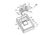
図1は第1実施形態に係る光モジュールの概略構成を示す分解斜視図、図2は光モジュールの概略構成を示す縦断面図である。図3(A)は光モジュール全体を示す斜視図、図3(B)はその光モジュールに用いる複数の光ファイバの1本を示す拡大図、図3(C)はその光モジュールに用いるレーザーダイオードアレイとドライバICの接続関係を示す平面図である。図4は光モジュールの概略構成を示す分解斜視図、図5は光モジュールの光コネクタ部を示す斜視図、図6はその光モジュールの光コネクタ部に外部のコネクタを装着した状態を示す斜視図である。 FIG. 1 is an exploded perspective view showing a schematic configuration of the optical module according to the first embodiment, and FIG. 2 is a longitudinal sectional view showing a schematic configuration of the optical module. 3A is a perspective view showing the entire optical module, FIG. 3B is an enlarged view showing one of a plurality of optical fibers used in the optical module, and FIG. 3C is a laser diode used in the optical module. It is a top view which shows the connection relation of an array and driver IC. 4 is an exploded perspective view showing a schematic configuration of the optical module, FIG. 5 is a perspective view showing an optical connector portion of the optical module, and FIG. 6 is a perspective view showing a state where an external connector is attached to the optical connector portion of the optical module. It is.
第1実施形態に係る光モジュール10は、図1、図2、図3(A)および図4に示すように、基板11と、光コネクタ部12と、カバー13と、ガイドピン32とを備えている。基板11は、セラミックス基板であり、その表面11aに電極パターン(図示省略)を有する。基板11の電極パターン上には、一列に整列して実装された複数の光素子と、複数の光素子と電気的に接続された電子素子と、を備える。本実施形態では、複数の光素子は、一列に整列された複数の面発光型半導体レーザ素子(光素子)を有するレーザーダイオードアレイ14で構成されている。図3(C)で符号14aは、レーザーダイオードアレイ14における複数の面発光型半導体レーザ素子の各光出射部(開口部)を示している。光素子としての面発光型半導体レーザ素子は、基板面に垂直な方向に光(光信号23)を出射するVCSEL(Vertical Cavity Surface Emitting Laser)である。また、電子素子は、レーザーダイオードアレイ14の複数の面発光型半導体レーザ素子を駆動するドライバIC15である。
The
レーザーダイオードアレイ14およびドライバIC15は、基板11の表面11aの電極パターン上に、例えばダイアタッチ剤で接着されて実装されている。レーザーダイオードアレイ14の複数の面発光型半導体レーザ素子とドライバIC15は、図3(A)および図3(C)に示すように、複数のワイヤ22でそれぞれ電気的に接続されている。これにより、ドライバIC15からレーザーダイオードアレイ14の複数の面発光型半導体レーザ素子には、ワイヤ22を介して変調信号が入力され、各面発光型半導体レーザ素子から変調信号により変調された光信号23が出射されるようになっている。また、ドライバIC15と基板11の電極パターンとは、複数のワイヤ(図示省略)で電気的に接続されている。
The
光コネクタ部12は、図5に示すように、複数の光ファイバ16を一列に(図2で紙面に垂直な方向に)整列させて保持している。この光コネクタ部12は、複数の光ファイバ16の各一端部16aの中心(コア中心)とレーザーダイオードアレイ14の複数の面発光型半導体レーザ素子の各光出射部14aの中心とが一致するようにアクティブ調芯した後、基板11の表面11a上に固定される。これにより、レーザーダイオードアレイ14の各面発光型半導体レーザ素子からの出射光(光信号23)は、複数の光ファイバ16の対応する光ファイバの一端部16aにそれぞれ光結合するようになっている。
As shown in FIG. 5, the
また、光コネクタ部12は左右の側壁部17を有する。両側壁部17の下端面17a(図5参照)が基板11の表面11aとそれぞれ摺動可能に接している。複数の光ファイバ16の各一端部16aの中心とレーザーダイオードアレイ14の各光出射部の中心とが一致するように、光コネクタ部12を基板11の表面11a内で二次元的に動かしてアクティブ調芯した後、光コネクタ部12の両側壁部17の下端面17aを基板11の表面11aに接着等により固定する。
The
さらに、光コネクタ部12は、図5に示すように、複数の光ファイバ16が挿入され、一列に整列して保持された複数のファイバ保持孔12aと、これらのファイバ保持孔12aの両側に設けられた2つのガイドピン孔12bとを有する。2つのガイドピン孔12bに、2つのガイドピン32がそれぞれ嵌合可能になっている。
Further, as shown in FIG. 5, the
2つのガイドピン32には、図6に示す外部のコネクタである多心用のフェルール型コネクタ(以下、MTコネクタという。)30の2つの貫通孔がそれぞれ嵌合可能になっている。MTコネクタ30の2つの貫通孔を2つのガイドピン32にそれぞれ嵌合させることにより、MTコネクタ30に保持された多心光ファイバ(多心テープ光ファイバ)31の各光ファイバの中心(コア中心)と、光コネクタ部12に保持された複数の光ファイバ16の各中心(コア中心)とが一致した状態で、MTコネクタ30が図6に示すように光コネクタ部12に装着されるようになっている。
Two guide holes 32 of a multi-core ferrule connector (hereinafter referred to as an MT connector) 30 as an external connector shown in FIG. The center of each optical fiber (core center) of the multi-core optical fiber (multi-core tape optical fiber) 31 held by the
カバー13は、図2および図4に示すように、光コネクタ部12を装着するための開口部13aを有し、レーザーダイオードアレイ14、ドライバIC15などの部品全体を覆うように基板11に接着等により固定される。このカバー13は、熱伝導率の高い材料、例えばCu(銅)とW(タングステン)の合金で作製されている。
As shown in FIGS. 2 and 4, the
光モジュール10の特徴は、以下の構成にある。
・光コネクタ部12は、図1および図5に示すように、複数の光ファイバ16が挿入された整列する複数のファイバ保持孔12aと、複数のファイバ保持孔12aの両側に、複数のファイバ保持孔12aの各中心に中心がそれぞれ一致した2つの貫通孔とを有する。本実施形態では、2つの貫通孔は2つのガイドピン32がそれぞれ嵌合する2つのガイドピン孔12bである。
The
As shown in FIGS. 1 and 5, the
・基板11の表面11a上には、図1および図5に示すように、2つのガイドピン孔(貫通孔)12bをそれぞれ通して視認可能で、光コネクタ部の位置決め基準となる2つのアライメントマーク50がレーザーダイオードアレイ14の外側に設けられている。
On the
また、この光モジュール10では、光コネクタ部12は、複数の光ファイバ16とレーザーダイオードアレイ14とがそれぞれ光結合するように光コネクタ部12の位置を調整するアクティブ調芯のために基板11の表面11a上で二次元的に移動可能である。つまり、光コネクタ部12は、複数の光ファイバ16の各一端部16aの中心(コア中心)とレーザーダイオードアレイ14の各光出射部14a(図3(C)参照)の中心とをそれぞれ一致させるアクティブ調芯を行うために、両側壁部17の下端面17aが基板11の表面11aとそれぞれ摺動可能に接しており、基板11上で二次元的に移動可能である。
In the
また、光コネクタ部12の基板11の表面11aと対向する一端面12c(図5参照)では、複数の光ファイバ16の各一端部16aが一列に整列して、レーザーダイオードアレイ14の各光出射部14aとそれぞれ対向している。また、光コネクタ部12の一端面12cとは反対側の他端面12dでは、複数の光ファイバ16の各他端部16bが一列に整列している。光コネクタ部12の側面とカバー13の開口部13aとの間の隙間には、図2に示すように樹脂封止剤或いは接着剤等の樹脂18が充填されている。
Further, at one
また、図1および図2に示すように、基板11の表面11aおよびこの表面に実装された部品と、カバー13との間のギャップ(空間)には、熱伝導率の高い封止剤が充填されている。具体的には、カバー13とドライバIC15との間の空間には、熱伝導性と絶縁性を有するシリコーンゲル19が封止剤として充填されている。また、複数の光ファイバ16の一端部16aとレーザーダイオードアレイ14の各光出射部14aとの間の空間には、透明なシリコーンゲル20が封止剤として充填されている。
<光モジュールの作製方法>
以上の構成を有する光モジュール10の作製方法を、図1に基づいて説明する。
Further, as shown in FIGS. 1 and 2, the
<Optical module manufacturing method>
A method of manufacturing the
光モジュール10の作製方法は、以下の工程(1)〜(6)を備える。
(1)基板11の表面11aの電極パターン上に整列したレーザーダイオードアレイ14とドライバIC15を実装し、レーザーダイオードアレイ14とドライバICをワイヤ22で電気的に接続する工程。
The manufacturing method of the
(1) A step of mounting the
(2)複数の光ファイバ16を整列させて保持した光コネクタ部12を基板11の表面11a上に載置する工程。
(2) A step of placing the
(3)光コネクタ部12を装着するための開口部13aを有するカバー13を基板11に固定する工程。
(3) A step of fixing the
(4)光コネクタ部12に設けられた2つのガイドピン孔(貫通孔)12bを通して、各ガイドピン孔12bの中心に基板11上に設けられたアライメントマーク50を視認できるように、光コネクタ部12を基板11上で二次元的に動かして光コネクタ部12の仮位置決め(粗い位置決め)を行う工程。
(4) The optical connector portion can be seen through the two guide pin holes (through holes) 12b provided in the
(5)光コネクタ部12の仮位置決め後に、光コネクタ部12を、複数の光ファイバ16の各一端部16aの中心とレーザーダイオードアレイ14の各光出射部14aの中心とがそれぞれ一致する位置に調整するアクティブ調芯を行う工程。
(5) After provisional positioning of the
(6)アクティブ調芯後に、光コネクタ部12を基板11の表面11a上に固定する工程。
(6) A step of fixing the
光コネクタ部12の仮位置決めを行う上記工程(4)では、図1に示すように、2つのガイドピン孔12bの各端部を、ガイドピン孔12bの中心軸とレンズの光軸を一致させたカメラ51で撮像して、各ガイドピン孔12b内部の画像情報を取得し、画像情報に基づき各ガイドピン孔12b内部の画像を表示手段としてのディスプレイ52により表示するのが好ましい。
In the step (4) for temporarily positioning the
以上のように構成された第1実施形態によれば、以下の作用効果を奏する。
○光コネクタ部12の2つのガイドピン孔12bを通して各ガイドピン孔12bの中心に2つのアライメントマーク50を視認できるように、光コネクタ部12を基板11上で二次元的に動かすことにより、光コネクタ部12の仮位置決めを行うことができる。このため、その仮位置決め後に行うアクティブ調芯時に光コネクタ部12を動かす量が少なくてすみ、アクティブ調芯を短時間で行うことができる。また、従来技術のように、パッシブアライメントを行うためのシリコン・オプティカルベンチ(SiOB)を内部に設ける必要が無く、その分部品点数の削減と小型化を図ることができる。
According to 1st Embodiment comprised as mentioned above, there exist the following effects.
By moving the
従って、アクティブ調芯を短時間で行うことができると共に、部品点数の削減と小型化を図ることができる光モジュール10を実現することができる。
Therefore, it is possible to realize the
○光コネクタ部12は基板11上で二次元的に移動可能であるので、光コネクタ部12の仮位置決め後に、アクティブ調芯を行って、複数の光ファイバ16の各一端部16aの中心とレーザーダイオードアレイ14の各光出射部14aの中心とがそれぞれ一致するように、光コネクタ部12の位置を調整することができる。
Since the
○ガイドピン32が嵌合する光コネクタ部12の2つのガイドピン孔12bを、アライメントマーク50を視認するための貫通孔として利用して光コネクタ部12の仮位置決めを行うので、2つのガイドピン孔12bを有する光コネクタ部12に特別な加工をする必要がない。
Since the
○カバー13の開口部13aと光コネクタ部12との間の隙間には、樹脂封止剤或いは接着剤等の樹脂18が充填されている。このため、複数の光ファイバ16の各一端部16aとレーザーダイオードアレイ14の各光出射部とが一致するようにアクティブ調芯した後、光モジュール12内部を樹脂封止剤気密に封止することができ、或いは光コネクタ部12をカバー13に固定することができる。
A
○上述した光モジュールの作製方法では、光コネクタ部12の仮位置決めを行う上記工程(4)において、図1に示すように、各ガイドピン孔12b内部の画像情報をカメラ51で取得し、取得した画像情報に基づき各ガイドピン孔12b内部の画像をディスプレイ52で表示する。これにより、ディスプレイ52で表示される各ガイドピン孔12b内部の画像を見ながら、各ガイドピン孔12bの中心にアライメントマーク50を視認できるように、光コネクタ部12を基板11上で二次元的に動かすことができる。このため、光コネクタ部12の仮位置決めを容易にかつ効率よく行うことができる。
In the above-described optical module manufacturing method, in the step (4) in which the
○上記工程(4)において、2つのガイドピン孔12bの各端部を、ガイドピン孔12bの中心軸とレンズの光軸を一致させたカメラ51で撮像して、各ガイドピン孔12b内部の画像情報を取得するので、ディスプレイ52で表示される画像は、2つのガイドピン孔12bの各端部を垂直方向から見た画像となる。このため、その画像を見ながら、光コネクタ部12の仮位置決めを正確に行うことができる。
In the step (4), each end of the two
(第2実施形態)
次に、第2実施形態に係る光モジュールを図7および図8に基づいて説明する。
(Second Embodiment)
Next, an optical module according to a second embodiment will be described with reference to FIGS.
上記第1実施形態に係る光モジュール10では、ガイドピン32が嵌合する光コネクタ部12の2つのガイドピン孔12bを、アライメントマーク50を視認するための貫通孔として利用している。これに対して、図7および図8に示す第2実施形態に係る光モジュール10Aでは、アライメントマーク50の外側に2つのアライメントマーク54が設けられている。そして、2つのアライメントマーク54を視認するための2つの貫通孔として、光コネクタ部12における2つのガイドピン孔12bの外側に、2つのガイドピン孔12bの中心に中心をそれぞれ一致させて設けられた孔(以下、アライメント用の貫通孔と呼ぶ)53を用いている。第2実施形態に係る光モジュール10Aのその他の構成は、上記第1実施形態に係る光モジュール10と同様である。
In the
以上のように構成された第2実施形態によれば、上記第1実施形態の奏する上記作用効果に加えて、以下の作用効果を奏する。 According to 2nd Embodiment comprised as mentioned above, in addition to the said effect produced by the said 1st Embodiment, there exist the following effects.
アライメントマーク50の外側に設けたアライメントマーク54を視認するための2つの貫通孔として、2つのガイドピン孔12bの外側に、2つのガイドピン孔12bの中心に中心をそれぞれ一致させて設けられたアライメント用の貫通孔53を用いている。これにより、光コネクタ部12にMTコネクタ30を装着した状態で、2つのアライメント用の貫通孔53を通して各貫通孔53の中心にアライメントマーク54を視認できるように、光コネクタ部12を基板11上で二次元的に動かすことにより、光コネクタ部12の仮位置決めを行うことができる。このため、その仮位置決め後に行うアクティブ調芯を、MTコネクタ30に保持された多心光ファイバ31に光をそれぞれ通して行うことができる。
As two through holes for visually recognizing the
(第3実施形態)
第3実施形態に係る光モジュール10Bを図9(A),(B)および図10に基づいて説明する。
(Third embodiment)
An
上記第1実施形態では、ドライバIC15を基板11の電極パターン上にワイヤボンディング実装している。これに対して、第3実施形態に係る光モジュール10Bでは、図9(A),(B)および図10に示すように、ドライバIC15を基板11の電極パターン上にフリップチップ実装している。また、この光モジュール10Bでは、レーザーダイオードアレイ14を、基板11に設けた凹部11c内に配置している。そして、レーザーダイオードアレイ14の複数の面発光型半導体レーザ素子とドライバIC15が接続された複数の配線(電極パターンの一部)とが、ワイヤ22でそれぞれ電気的に接続されている。光モジュール10Bのその他の構成は、上記第1実施形態に係る光モジュール10と同様である。
In the first embodiment, the
このような構成を有する第3実施形態に係る光モジュール10Bによれば、ドライバIC15を基板11の電極パターン上にフリップチップ実装した光モジュールにおいて、上記第1実施形態と同様にアクティブ調芯を短時間で行うことができると共に、部品点数の削減と小型化を図ることができる光モジュール10を実現することができる。
According to the
なお、この発明は以下のように変更して具体化することもできる。
・上記各実施形態では、送信側光モジュールとして構成した光モジュール10,10Aについて説明したが、本発明はこれに限定されない。光モジュール10,10Aにおいて、レーザーダイオードアレイ14に代えて一列に整列された複数のフォトダイオード素子(光素子)を有するフォトダイオードアレイを用いる。そして、ドライバIC15に代えて、各フォトダイオードの出力電流を電圧に変換して増幅する(TIA:Transimpedance Amplifier)の機能を備えた増幅用ICを用いて受信側光モジュールとして構成した光モジュールにも本発明は適用可能である。
In addition, this invention can also be changed and embodied as follows.
In each of the above embodiments, the
・また、レーザーダイオードアレイ14に代えて、複数の面発光型半導体レーザ素子(光素子)が一列に整列されて実装された光モジュール、或いは、フォトダイオードアレイに代えて複数のフォトダイオード(光素子)が一列に整列されて実装された光モジュールにも本発明は適用可能である。
An optical module in which a plurality of surface emitting semiconductor laser elements (optical elements) are arranged in a line instead of the
10,10A,10B:光モジュール
11:基板
11a:表面
12:光コネクタ部
12a:ファイバ保持孔
12b:ガイドピン孔(貫通孔)
13:カバー
13a:開口部
14:面発光型半導体レーザ(光素子)
15:ドライバIC(電子素子)
16:光ファイバ
16a:一端部
23:光信号
30:多心用のフェルール型コネクタ(MTコネクタ)
31:多心光ファイバ(多心テープ光ファイバ)
50,54:アライメントマーク
51:カメラ
52:表示手段としてのディスプレイ
53:アライメント用の貫通孔
10, 10A, 10B: optical module 11:
13:
15: Driver IC (electronic element)
16:
31: Multi-core optical fiber (multi-fiber tape optical fiber)
50, 54: Alignment mark 51: Camera 52: Display as display means 53: Through hole for alignment
Claims (9)
前記基板上に実装された複数の光素子と、
前記基板上に実装され、前記複数の光素子と電気的に接続された電子素子と、
複数の光ファイバを保持し、前記複数の光ファイバと前記複数の光素子とがそれぞれ光結合する位置で前記基板に固定される光コネクタ部と、
前記光コネクタ部を装着するための開口部を有し、前記複数の光素子と前記電子素子を含む部品全体を覆うように前記基板に固定されるカバーと、を備え、
前記光コネクタ部は、前記複数の光ファイバが挿入、保持された複数のファイバ保持孔と、前記複数のファイバ保持孔の両側に、前記複数のファイバ保持孔の各中心に中心がそれぞれ一致した2つの貫通孔とを有し、
前記基板の表面上には、前記2つの貫通孔をそれぞれ通して視認可能で、前記光コネクタ部の位置決め基準となる2つのアライメントマークが設けられていることを特徴とする光モジュール。 A substrate,
A plurality of optical elements mounted on the substrate;
An electronic element mounted on the substrate and electrically connected to the plurality of optical elements;
An optical connector portion that holds a plurality of optical fibers and is fixed to the substrate at a position where the plurality of optical fibers and the plurality of optical elements are respectively optically coupled,
A cover that has an opening for mounting the optical connector portion, and is fixed to the substrate so as to cover the entire component including the plurality of optical elements and the electronic element;
The optical connector portion includes a plurality of fiber holding holes into which the plurality of optical fibers are inserted and held, and two centers of the plurality of fiber holding holes, the centers of which coincide with the centers of the plurality of fiber holding holes, respectively. With two through holes,
On the surface of the substrate, two alignment marks that are visible through the two through holes and serve as a positioning reference for the optical connector portion are provided.
基板上に整列した複数の光素子と電子素子を実装し、複数の光素子と電子素子を電気的に接続する工程と、
複数の光ファイバを保持した光コネクタ部を前記基板上に載置する工程と、
前記光コネクタ部を装着するための開口部を有するカバーを前記基板に固定する工程と、
前記光コネクタ部に設けられた2つの貫通孔を通して、各貫通孔の中心に前記基板上に設けられたアライメントマークを視認できるように、前記光コネクタ部を前記基板上で二次元的に動かして前記光コネクタ部の仮位置決めを行う工程と、
前記光コネクタ部の仮位置決め後に、該光コネクタ部を、前記複数の光ファイバと前記複数の光素子とがそれぞれ光結合する位置に調整するアクティブ調芯を行う工程と、
前記アクティブ調芯後に、前記光コネクタ部を前記基板上に固定する工程と、
を備えることを特徴とする光モジュールの作製方法。 An optical module manufacturing method comprising:
Mounting a plurality of optical elements and electronic elements aligned on a substrate and electrically connecting the plurality of optical elements and electronic elements;
Placing an optical connector portion holding a plurality of optical fibers on the substrate;
Fixing a cover having an opening for mounting the optical connector portion to the substrate;
The optical connector is moved two-dimensionally on the substrate so that the alignment mark provided on the substrate can be visually recognized at the center of each through-hole through the two through-holes provided in the optical connector. Performing temporary positioning of the optical connector part;
After the temporary positioning of the optical connector part, performing the active alignment to adjust the optical connector part to a position where the plurality of optical fibers and the plurality of optical elements are respectively optically coupled;
After the active alignment, fixing the optical connector part on the substrate;
An optical module manufacturing method comprising:
Priority Applications (2)
| Application Number | Priority Date | Filing Date | Title |
|---|---|---|---|
| JP2008007441A JP4477677B2 (en) | 2008-01-16 | 2008-01-16 | Optical module and manufacturing method thereof |
| US12/352,846 US8366325B2 (en) | 2008-01-16 | 2009-01-13 | Optical module and method of manufacturing thereof |
Applications Claiming Priority (1)
| Application Number | Priority Date | Filing Date | Title |
|---|---|---|---|
| JP2008007441A JP4477677B2 (en) | 2008-01-16 | 2008-01-16 | Optical module and manufacturing method thereof |
Publications (2)
| Publication Number | Publication Date |
|---|---|
| JP2009169116A true JP2009169116A (en) | 2009-07-30 |
| JP4477677B2 JP4477677B2 (en) | 2010-06-09 |
Family
ID=40970349
Family Applications (1)
| Application Number | Title | Priority Date | Filing Date |
|---|---|---|---|
| JP2008007441A Active JP4477677B2 (en) | 2008-01-16 | 2008-01-16 | Optical module and manufacturing method thereof |
Country Status (2)
| Country | Link |
|---|---|
| US (1) | US8366325B2 (en) |
| JP (1) | JP4477677B2 (en) |
Cited By (2)
| Publication number | Priority date | Publication date | Assignee | Title |
|---|---|---|---|---|
| JP2011183987A (en) * | 2010-03-10 | 2011-09-22 | Autonetworks Technologies Ltd | Circuit constituting body and electrical connection box |
| JP2012093536A (en) * | 2010-10-27 | 2012-05-17 | Japan Aviation Electronics Industry Ltd | Optical module |
Families Citing this family (14)
| Publication number | Priority date | Publication date | Assignee | Title |
|---|---|---|---|---|
| WO2009090988A1 (en) * | 2008-01-16 | 2009-07-23 | The Furukawa Electric Co., Ltd. | Optical module |
| US8699012B2 (en) * | 2010-03-17 | 2014-04-15 | Tyco Electronics Nederland B.V. | Optical fiber alignment measurement method and apparatus |
| US8538215B2 (en) * | 2010-05-20 | 2013-09-17 | Analog Devices, Inc. | Optical package and related methods |
| US8842951B2 (en) | 2012-03-02 | 2014-09-23 | Analog Devices, Inc. | Systems and methods for passive alignment of opto-electronic components |
| US9716193B2 (en) | 2012-05-02 | 2017-07-25 | Analog Devices, Inc. | Integrated optical sensor module |
| EP2892587A1 (en) * | 2012-09-04 | 2015-07-15 | Fenwal, Inc. | Interface detector for blood processing system |
| WO2014179511A2 (en) * | 2013-04-30 | 2014-11-06 | Finisar Corporation | Thermal management structures for optoelectronic modules |
| US10884551B2 (en) | 2013-05-16 | 2021-01-05 | Analog Devices, Inc. | Integrated gesture sensor module |
| US9590129B2 (en) | 2014-11-19 | 2017-03-07 | Analog Devices Global | Optical sensor module |
| KR102356288B1 (en) * | 2015-03-03 | 2022-02-03 | 한국전자통신연구원 | Optical coupling device |
| JP6183527B1 (en) * | 2016-09-30 | 2017-08-23 | 富士通オプティカルコンポーネンツ株式会社 | Optical module and optical modulator |
| US10712197B2 (en) | 2018-01-11 | 2020-07-14 | Analog Devices Global Unlimited Company | Optical sensor package |
| WO2021087122A1 (en) * | 2019-10-29 | 2021-05-06 | Ipg Photonics Corporation | Optical fiber cable connector |
| CN112059065B (en) * | 2020-07-28 | 2023-04-28 | 宿迁学院 | Diode pin shaping device |
Family Cites Families (16)
| Publication number | Priority date | Publication date | Assignee | Title |
|---|---|---|---|---|
| EP1063549A4 (en) * | 1998-12-25 | 2006-07-12 | Sumitomo Electric Industries | Transmitter/receiver for optical parallel transmission and board for optical module |
| JP2000199837A (en) | 1999-01-06 | 2000-07-18 | Sumitomo Electric Ind Ltd | Optical parallel transmitting transceiver |
| JP3824797B2 (en) * | 1999-01-08 | 2006-09-20 | 古河電気工業株式会社 | Light emitting / receiving element module |
| US6641310B2 (en) * | 2000-04-21 | 2003-11-04 | Teraconnect, Inc. | Fiber optic cable connector |
| JP2002202440A (en) | 2000-12-28 | 2002-07-19 | Japan Aviation Electronics Industry Ltd | Structure and method of mounting optical module |
| US6736553B1 (en) * | 2001-01-12 | 2004-05-18 | Optical Communication Products, Inc. | VCSEL array optical subassembly module with alignment mechanism |
| JP3672831B2 (en) | 2001-02-27 | 2005-07-20 | 住友電気工業株式会社 | Mounting board and optical module |
| US6635866B2 (en) * | 2001-04-19 | 2003-10-21 | Internation Business Machines Corporation | Multi-functional fiber optic coupler |
| US6910812B2 (en) * | 2001-05-15 | 2005-06-28 | Peregrine Semiconductor Corporation | Small-scale optoelectronic package |
| US6676302B2 (en) * | 2001-09-17 | 2004-01-13 | Stratos Lightwave, Inc. | Method of constructing a fiber optics communications module |
| US6739760B2 (en) * | 2001-09-17 | 2004-05-25 | Stratos International, Inc. | Parallel fiber optics communications module |
| US6748145B2 (en) | 2001-12-20 | 2004-06-08 | Eastman Kodak Company | Fiber optic array and method of making same |
| US6950570B1 (en) * | 2002-08-13 | 2005-09-27 | Active Optical Networks, Inc. | Integrated fiber, sensor and lens arrays for optical networks |
| US20040190851A1 (en) * | 2003-03-31 | 2004-09-30 | Garner Sean M. | Two-dimensional optical element arrays |
| JP4559327B2 (en) | 2005-09-14 | 2010-10-06 | 株式会社日立製作所 | Alignment method of optical module using lens and optical module created by the method |
| WO2008096716A1 (en) * | 2007-02-05 | 2008-08-14 | Nippon Telegraph And Telephone Corporation | Semiconductor submodule, method for connecting connector and semiconductor submodule, and optical module |
-
2008
- 2008-01-16 JP JP2008007441A patent/JP4477677B2/en active Active
-
2009
- 2009-01-13 US US12/352,846 patent/US8366325B2/en active Active
Cited By (2)
| Publication number | Priority date | Publication date | Assignee | Title |
|---|---|---|---|---|
| JP2011183987A (en) * | 2010-03-10 | 2011-09-22 | Autonetworks Technologies Ltd | Circuit constituting body and electrical connection box |
| JP2012093536A (en) * | 2010-10-27 | 2012-05-17 | Japan Aviation Electronics Industry Ltd | Optical module |
Also Published As
| Publication number | Publication date |
|---|---|
| US8366325B2 (en) | 2013-02-05 |
| US20090269006A1 (en) | 2009-10-29 |
| JP4477677B2 (en) | 2010-06-09 |
Similar Documents
| Publication | Publication Date | Title |
|---|---|---|
| JP4477677B2 (en) | Optical module and manufacturing method thereof | |
| JP5065062B2 (en) | Optical module | |
| JP5625138B1 (en) | Optical module, optical module mounting method, optical module mounting circuit board, optical module evaluation kit system, circuit board, and communication system | |
| WO2009090988A1 (en) | Optical module | |
| EP2790048A1 (en) | Optical module | |
| JP2008040318A (en) | Manufacturing method of multi-channel optical module | |
| US20090323748A1 (en) | Photoelectric conversion device, photoelectric conversion module and method of manufacturing photoelectric conversion device | |
| US20170261701A1 (en) | Optical module | |
| US10018791B2 (en) | Multi-channel optical subassembly and method of manufacturing the same | |
| US8750657B2 (en) | Flip-chip optical interface with micro-lens array | |
| JP2011099930A (en) | Optical transmitter-receiver | |
| JP2015028658A (en) | Optical module, optical module mounting method, optical module mounted circuit board, optical module evaluation kit system, circuit board, and communication system | |
| US9297967B2 (en) | Device for converting signal | |
| JP2005292739A (en) | Optical module | |
| JP5065061B2 (en) | Optical module | |
| JP2011164143A (en) | Optical module | |
| KR20080088723A (en) | Parallel optical transceiver module package using guide pin | |
| JP2004085756A (en) | Optical transmission/reception module | |
| KR101256814B1 (en) | All passive aligned optical module and manufacturing method thereof | |
| JP2022037163A (en) | Optical subassembly, optical module, and optical transmission device | |
| JP6421557B2 (en) | Optical module and optical cable | |
| JP3452120B2 (en) | Optical module and optical transceiver | |
| JP2008090093A (en) | Single-core bidirectional optical transmission and reception transceiver | |
| JP2004341370A (en) | Optical module | |
| KR20110105605A (en) | Optoelectonic device package |
Legal Events
| Date | Code | Title | Description |
|---|---|---|---|
| A977 | Report on retrieval |
Free format text: JAPANESE INTERMEDIATE CODE: A971007 Effective date: 20091105 |
|
| A131 | Notification of reasons for refusal |
Free format text: JAPANESE INTERMEDIATE CODE: A131 Effective date: 20091116 |
|
| A521 | Request for written amendment filed |
Free format text: JAPANESE INTERMEDIATE CODE: A523 Effective date: 20100113 |
|
| TRDD | Decision of grant or rejection written | ||
| A01 | Written decision to grant a patent or to grant a registration (utility model) |
Free format text: JAPANESE INTERMEDIATE CODE: A01 Effective date: 20100305 |
|
| A01 | Written decision to grant a patent or to grant a registration (utility model) |
Free format text: JAPANESE INTERMEDIATE CODE: A01 |
|
| A61 | First payment of annual fees (during grant procedure) |
Free format text: JAPANESE INTERMEDIATE CODE: A61 Effective date: 20100311 |
|
| R151 | Written notification of patent or utility model registration |
Ref document number: 4477677 Country of ref document: JP Free format text: JAPANESE INTERMEDIATE CODE: R151 |
|
| FPAY | Renewal fee payment (event date is renewal date of database) |
Free format text: PAYMENT UNTIL: 20130319 Year of fee payment: 3 |
|
| FPAY | Renewal fee payment (event date is renewal date of database) |
Free format text: PAYMENT UNTIL: 20130319 Year of fee payment: 3 |
|
| FPAY | Renewal fee payment (event date is renewal date of database) |
Free format text: PAYMENT UNTIL: 20140319 Year of fee payment: 4 |
|
| S531 | Written request for registration of change of domicile |
Free format text: JAPANESE INTERMEDIATE CODE: R313531 |
|
| R350 | Written notification of registration of transfer |
Free format text: JAPANESE INTERMEDIATE CODE: R350 |