JP2005292739A - Optical module - Google Patents
Optical module Download PDFInfo
- Publication number
- JP2005292739A JP2005292739A JP2004111688A JP2004111688A JP2005292739A JP 2005292739 A JP2005292739 A JP 2005292739A JP 2004111688 A JP2004111688 A JP 2004111688A JP 2004111688 A JP2004111688 A JP 2004111688A JP 2005292739 A JP2005292739 A JP 2005292739A
- Authority
- JP
- Japan
- Prior art keywords
- optical
- translucent plate
- substrate
- optical module
- component
- Prior art date
- Legal status (The legal status is an assumption and is not a legal conclusion. Google has not performed a legal analysis and makes no representation as to the accuracy of the status listed.)
- Pending
Links
Images
Landscapes
- Optical Couplings Of Light Guides (AREA)
- Semiconductor Lasers (AREA)
- Light Receiving Elements (AREA)
Abstract
【課題】光素子が透光性板に半田によって実装される光モジュールにおいて、光結合だけでなく電気的結合も高精度で簡単に位置あわせ実装を可能にする機構を有する光モジュールを提供すること。
【解決手段】ファイバブロック1と透光性板4と基板9それぞれに設けられたガイド穴2a、2b、2cをガイドピン7によって嵌合させることで、光素子6とファイバブロック1に固定されたファイバ3は光結合がなされ、透光性板4上の導電性パターン5と基板9の導電性パターン上に置かれた半田8との電気的接続も行われる。
【選択図】図1
In an optical module in which an optical element is mounted on a translucent plate by soldering, an optical module having a mechanism that enables not only optical coupling but also electrical coupling to be easily aligned and mounted with high accuracy is provided. .
Guide holes 2a, 2b and 2c provided in a fiber block 1, a translucent plate 4 and a substrate 9 are fitted by guide pins 7 so that the optical element 6 and the fiber block 1 are fixed. The fiber 3 is optically coupled, and electrical connection between the conductive pattern 5 on the translucent plate 4 and the solder 8 placed on the conductive pattern on the substrate 9 is also performed.
[Selection] Figure 1
Description
本発明は、光信号を送信もしくは受信する光モジュールの構造に関するものである。 The present invention relates to a structure of an optical module that transmits or receives an optical signal.
近年、インターネットの急速な普及に伴い、サービスプロバイダーのバックボーン光ネットワークの伝送容量は急激に増大している。そのため、大容量のルータや光多重伝送装置等が置かれる局舎内では、各装置内あるいは装置間を接続する大容量、低価格、低消費電力の光モジュールの需要が高まっている。
このような要求を満たす光モジュールは、多々提案されているが、低価格、低消費電力の観点から、発光光源としてVCSEL(Vertical Cavity Surface Emitting Laser)に代表される面発光素子と共に、光電変換をPINフォトダイオードに代表される面型受光素子によって行う方式が取られている。更に大容量化の観点から、これらの光素子を250μmピッチで複数チャンネル並べたアレイ型光素子が用いられている。VCSELは電気的に接続されたICによって駆動変調され、面型受光素子で光電変換された電気信号は電気的に接続されたICによって増幅され出力される。
In recent years, with the rapid spread of the Internet, the transmission capacity of a service provider's backbone optical network has increased rapidly. Therefore, in a station where a large-capacity router, an optical multiplex transmission apparatus, and the like are placed, there is an increasing demand for a large-capacity, low-cost, low-power-consumption optical module that connects each apparatus or between apparatuses.
Many optical modules that meet these requirements have been proposed, but from the viewpoint of low cost and low power consumption, photoelectric conversion is performed together with a surface light emitting device represented by VCSEL (Vertical Cavity Surface Emitting Laser) as a light source. A method using a surface light-receiving element typified by a PIN photodiode is employed. Further, from the viewpoint of increasing the capacity, an array type optical element in which a plurality of channels of these optical elements are arranged at a pitch of 250 μm is used. The VCSEL is driven and modulated by an electrically connected IC, and an electric signal photoelectrically converted by the surface light receiving element is amplified and output by the electrically connected IC.
このような光モジュールの光学系の一例として特開2001−116962が知られている。これは250μmピッチのアレイ状光素子を光素子搭載用基板上に実装し、250μmピッチのアレイレンズを介して250μmピッチの多芯光ファイバと光結合を行う。一般的な面型光素子の場合、発光面/受光面は電気パッドと同じ面上にあるため電気パッドにワイヤボンディングがなされる。このワイヤに接触しないようにするために、アレイレンズ−光素子間距離は数百μm〜数mm程度離間させる必要があった。しかし一般的なVCSELの空間中の広がり角は30°程度にも及ぶため、アレイレンズ−光素子間距離が長いと、隣接チャンネルに光信号がもれこんでしまう光学的クロストークが発生する。更に250μmピッチのアレイレンズではレンズ直径を250μm以上にすることは出来ないため、VCSEL−アレイレンズ間距離を長くするとビームスポットが大きくなり、収差によって光結合が劣化する等の問題があった。 Japanese Patent Laid-Open No. 2001-116962 is known as an example of an optical system of such an optical module. In this method, an arrayed optical element having a pitch of 250 μm is mounted on an optical element mounting substrate and optically coupled to a multicore optical fiber having a pitch of 250 μm through an array lens having a pitch of 250 μm. In the case of a general surface type optical element, since the light emitting surface / light receiving surface is on the same surface as the electric pad, wire bonding is performed on the electric pad. In order not to come into contact with the wire, the distance between the array lens and the optical element needs to be separated by several hundred μm to several mm. However, since the spread angle in the space of a general VCSEL reaches about 30 °, an optical crosstalk in which an optical signal leaks into an adjacent channel occurs when the distance between the array lens and the optical element is long. Furthermore, since the lens diameter cannot be increased to 250 μm or more with an array lens having a pitch of 250 μm, when the distance between the VCSEL and the array lens is increased, the beam spot is increased, and optical coupling is deteriorated due to aberration.
これらの問題を解決した例として、図15に2003年電子情報通信学会ソサイエティ大会講演論文集C−3−124に示される従来の光モジュールの断面構造を示す。この光モジュールでは、光素子6は半田8によって透明樹脂基板16上の導電性パターン5上にフリップチップ実装されている。したがって光素子6の発光面/受光面は上側となる。アレイレンズ基板11はレンズホルダ15によって固定され、透明樹脂基板16上に実装される。光コネクタ20のV溝21に配線保持された光ファイバ3と光素子6との光結合はガイドピン7を透明樹脂基板上に設けられたガイド穴2に嵌合させることで行われる。したがって、たとえば光素子6が発光素子の場合、光線は透明樹脂基板16、アレイレンズ基板11を透過後、ミラー面22で反射され光ファイバ3内に入射される。LSI18も透明樹脂基板16上にフリップチップ実装されるため、光素子6とLSI18との電気的接続は透明樹脂基板16上の導電性パターン5を介して行われる。さらに透明樹脂基板16上の導電性パターン5とセラミック基板19上の導電性パターン5、スルーホール10及びコンデンサ17との電気的接続は半田8を介して行われる。
As an example of solving these problems, FIG. 15 shows a cross-sectional structure of a conventional optical module shown in C-2003-124 Proceedings of Society Conference of the Institute of Electronics, Information and Communication Engineers of Japan. In this optical module, the
図15に示す光モジュールの利点は光素子6をワイヤを使うことなく半田8によって電気接続を行うので、アレイレンズ11−光素子6間の光路長はほぼ透明樹脂基板16の厚さによって精度良く決めることが出来る。一般的に透明樹脂基板16は現行の技術で50μm程度まで薄くできるので、隣接チャンネルに光信号が漏れ込む恐れや、アレイレンズ基板11のレンズ11での収差による光結合劣化も防ぐことが出来る。
また他の一つの利点は、光コネクタ20のV溝21に固定されたファイバ3と透明樹脂基板16に固定された光素子6との光結合が、ガイドピン7とガイド穴2との嵌合によって簡単に数μm程度の精度で行えることである。
The advantage of the optical module shown in FIG. 15 is that the
Another advantage is that the optical coupling between the fiber 3 fixed to the V groove 21 of the
しかしながら、図15に示すに光モジュールおいては次の課題を有する。参考文献2003年電子情報通信学会ソサイエティ大会講演論文集C−3−124によると、透明樹脂基板16のサイズは10mm×11mm程度である。したがって、透明樹脂基板16上に、多チャンネルの電気信号、電源、グランドの導電性パターン5がパターニングされる必要があり、これらは数十本にも及ぶ。したがって導電性パターン5の幅および導電性パターン5同士の間隔は数十〜数百μm程度と非常に細い。導電性パターン5には高周波信号が流れるため、透明樹脂基板16上導電性パターン5とセラミック基板19上の導電性パターン5は、数〜数十μm程度の精度で位置あわせ後、電気的接続がなされなければならない。
However, the optical module shown in FIG. 15 has the following problems. According to the reference literature C-3-124 of the 2003 IEICE Society Conference, the size of the
そこで本発明の目的は以上の課題を解決するために、光素子が透光性板に半田によって実装される光モジュールにおいて、光結合だけでなく電気的結合も数μm程度の精度で簡単に位置あわせ実装を可能にする機構を有する光モジュールを提供することである。 Accordingly, in order to solve the above problems, the object of the present invention is to easily position not only optical coupling but also electrical coupling with an accuracy of several μm in an optical module in which an optical element is mounted on a light-transmitting plate by solder. Another object of the present invention is to provide an optical module having a mechanism that enables mounting.
本発明の光モジュールは、面型光素子、透光性板、光部品、透光性板を搭載する台座を有した基板から構成される。面型光素子は、透光性板の導電性パターン上に搭載されている。光部品は面型光素子と光結合がなされる。透光性板を搭載するための基板上の台座部は、導電性パターンを有している。透光性板、光部品のうち少なくとも一つ、基板は、それぞれガイドピンがついているか、もしくはガイドピンをガイドする機構をもっている。このガイドピンとガイド機構は嵌合させられることで、光素子と光部品の光学的結合がなされ、透光性板上の導電性パターンと台座上の導電性パターンは電気的接合がなされることが特徴である。 The optical module of the present invention is composed of a planar optical element, a translucent plate, an optical component, and a substrate having a base on which the translucent plate is mounted. The planar optical element is mounted on the conductive pattern of the translucent plate. The optical component is optically coupled to the surface optical element. The pedestal on the substrate for mounting the translucent plate has a conductive pattern. At least one of the translucent plate and the optical component and the substrate each have a guide pin or a mechanism for guiding the guide pin. The guide pin and the guide mechanism are fitted to each other so that the optical element and the optical component are optically coupled, and the conductive pattern on the translucent plate and the conductive pattern on the base are electrically connected. It is a feature.
面型光素子とは面型発光/受光素子であり、発光面/受光面と同じ面側に電気信号入出力用の電気パッドがある。光素子は、光信号が透光性板内を透過するように透光性板上に搭載される。透光性板上の導電性パターンと光素子の電極パッドは半田等の金属によって接着され電気接続される。
透光性板とは光信号の一部の光を透過すれば良く、平板、レンズ、偏光板、波長板、フィルタ、ミラー等でも良い。
導電性パターンとは、導電性を有した材質で出来ている。
2つの導電性パターンの電気的接続は、半田、ペースト半田、接触等で行われ、電気信号の少なくとも一部が伝導すればよい。
A surface optical element is a surface light emitting / receiving element, and an electric pad for inputting / outputting electric signals is provided on the same side as the light emitting / receiving surface. The optical element is mounted on the translucent plate so that the optical signal is transmitted through the translucent plate. The conductive pattern on the translucent plate and the electrode pad of the optical element are bonded and electrically connected by a metal such as solder.
The light-transmitting plate may transmit a part of light of the optical signal, and may be a flat plate, a lens, a polarizing plate, a wave plate, a filter, a mirror, or the like.
The conductive pattern is made of a conductive material.
The electrical connection between the two conductive patterns is performed by solder, paste solder, contact, or the like, and it is sufficient that at least a part of the electrical signal is conducted.
光部品とは、少なくとも光信号の一部が透過するものであれば、平板、レンズ、偏光板、波長板、フィルタ、ミラー等などである。
光素子と光部品の光学的結合は、外部の光モジュールと送受信する光信号の少なくとも一部が光部品を透過すれば成すことが出来る。
基板上に透光性板用の台座を設けるが、台座の材質は底面の基板と同じ材質でも別の材質でもよい。また台座は基板に固定されているか一体化されている。
ガイドピンの材質は金属、セラミック等で出来ている。またガイドピンは光モジュール内の部品と別体でも良く、一体化されていても良い。
ガイドピンとガイドピンをガイドする機構とは、特開平7−209556、特開平8−136768、特開平10−239570などが知られている。
The optical component is a flat plate, a lens, a polarizing plate, a wavelength plate, a filter, a mirror, or the like as long as at least a part of the optical signal is transmitted.
The optical coupling between the optical element and the optical component can be achieved if at least part of the optical signal transmitted to and received from the external optical module passes through the optical component.
A pedestal for the translucent plate is provided on the substrate, and the material of the pedestal may be the same as or different from the substrate on the bottom surface. The pedestal is fixed to or integrated with the substrate.
The material of the guide pin is made of metal or ceramic. The guide pins may be separate from the components in the optical module or may be integrated.
JP-A-7-209556, JP-A-8-136768, JP-A-10-239570, and the like are known as a guide pin and a mechanism for guiding the guide pin.
本光モジュールでは、基板、透光性板、光部品に設けられたガイドピンまたはガイド溝の嵌合によって、光部品と光素子の光結合がなされ、透光性板上の導電性パターンと基板台座上の導電性パターンは電気結合が精度良くなされる。
本発明の光モジュールは、少なくとも一つの電子部品が基板上に搭載されていて、ガイドピンとガイド機構を嵌合されることで、光素子と光部品の光学的結合がなされ、透光性板の導電性パターンと電子部品の電極パッドは電気的接合がなされることを特徴とする。
電子部品とはIC、容量素子、インダクタンス素子、抵抗素子等の電気信号を通すもの、電気信号を変化させる機能を持つものであれば何でも良い。
In this optical module, the optical component and the optical element are optically coupled by fitting a guide pin or a guide groove provided on the substrate, the translucent plate, or the optical component, and the conductive pattern on the translucent plate and the substrate are coupled. The conductive pattern on the pedestal is electrically coupled with high accuracy.
In the optical module of the present invention, at least one electronic component is mounted on the substrate, and the optical pin and the optical component are optically coupled by fitting the guide pin and the guide mechanism. The conductive pattern and the electrode pad of the electronic component are electrically connected.
The electronic component may be anything as long as it can pass an electric signal such as an IC, a capacitive element, an inductance element, a resistance element, or the like, and has a function of changing the electric signal.
電子部品の電極パッドと透光性板上の導電性パターンは半田、導電性ペースト等の導電性の材料で固着されているか接触されて電気伝導がなされている。
本発明の光モジュールでは、基板、透光性板、光部品に設けられたガイドピンまたはガイド溝の嵌合によって、光部品と光素子の光結合がなされ、透光性板上の導電性パターンと電子部品の電極パッドは電気結合が精度良くなされる。
少なくとも一つの電子部品が透光性板上に搭載されている光モジュールにおいて、透光性板上に実装される電子部品とはIC、容量素子、インダクタンス素子、抵抗素子等の電気信号を通すもの、電気信号変化させる機能を有していれば何でも良い。
The electrode pad of the electronic component and the conductive pattern on the light-transmitting plate are fixed or contacted with a conductive material such as solder or conductive paste to conduct electrical conduction.
In the optical module of the present invention, the optical component and the optical element are optically coupled by fitting the guide pin or the guide groove provided on the substrate, the translucent plate, or the optical component, and the conductive pattern on the translucent plate. The electrode pads of the electronic parts are electrically coupled with high accuracy.
In an optical module in which at least one electronic component is mounted on a translucent plate, the electronic component mounted on the translucent plate passes an electrical signal such as an IC, a capacitive element, an inductance element, or a resistance element. Anything can be used as long as it has a function of changing an electric signal.
電子部品の電極パッドと透光性板上の導電性パターンは半田、導電性ペースト等の導電性の材料で固着されている。
本発明の光モジュールでは電子部品を透光性板上に実装することで、透光性板上のスペースを有効に利用することが出来ると共に、電子部品、光素子間の距離が近くなることで電気信号の高周波伝導特性が良好になる。
光部品が基板に設けられた光部品用の台座上に搭載される光モジュールにおいては、透光性板に外部から圧力等がかからないように、光部品の透光性板側の高さが透光性板の光部品側の高さと同じか、高い位置に搭載されるようになっている。本発明の光モジュールでは、透光性板の上方にある光部品に加わる外力が透光性板に加わらないため、機械的信頼性が保つことができる。
The electrode pad of the electronic component and the conductive pattern on the translucent plate are fixed with a conductive material such as solder or conductive paste.
In the optical module of the present invention, by mounting the electronic component on the translucent plate, the space on the translucent plate can be used effectively, and the distance between the electronic component and the optical element is reduced. The high frequency conduction characteristics of the electric signal are improved.
In an optical module in which an optical component is mounted on a base for an optical component provided on a substrate, the height of the optical component on the side of the translucent plate is transparent so that no pressure is applied to the translucent plate from the outside. The optical plate is mounted at the same height as or higher than the height of the optical component side. In the optical module of the present invention, the external force applied to the optical component above the translucent plate is not applied to the translucent plate, so that mechanical reliability can be maintained.
光部品を搭載する台座の材質は、台座を搭載している基板と同じ材質でも別の材質でもよい。また台座は基板に固定されているか一体化されている。
光部品を搭載する台座は透光性板を搭載する台座と少なくとも一部が一体化されていても良い。
透光性板が搭載される台座で囲まれた内側が凹部になっていて、この凹部の位置に透光性板上に搭載された光素子が位置している光モジュールでは、光素子の周囲が透光性板、透光性板用台座、基板によって囲まれるため、外気の塵等が光素子が搭載されている部分に混入しにくいという利点を持つ。
The material of the pedestal on which the optical component is mounted may be the same as or different from the substrate on which the pedestal is mounted. The pedestal is fixed to or integrated with the substrate.
The pedestal on which the optical component is mounted may be at least partially integrated with the pedestal on which the translucent plate is mounted.
In the optical module in which the inner side surrounded by the pedestal on which the translucent plate is mounted is a recess, and the optical element mounted on the translucent plate is located at the position of the recess, the periphery of the optical element Is surrounded by a translucent plate, a translucent plate base, and a substrate, and therefore has an advantage that dust or the like of outside air is not easily mixed into a portion where the optical element is mounted.
また台座と透光性板を接着剤・樹脂・半田等で光素子の周囲を取り囲むように固着することで、光素子が外気にさらされない信頼性の高い光モジュールを作ることが出来る。
透光性板の周囲を取り囲むように光部品を搭載する台座が基板上に設けられていることを特徴とする光モジュールでは、光部品の透光性板側の面が透光性板の光部品側の面と同じ高さか高くなるように配置されている。光部品、光部品用台座、基板で囲まれる部分は、光部品によって外気からの塵等の混入が防がれており、光素子や透光性板を塵等の汚濁から防いでいる。
Further, by fixing the pedestal and the translucent plate so as to surround the periphery of the optical element with an adhesive, resin, solder or the like, a highly reliable optical module in which the optical element is not exposed to the outside air can be produced.
In an optical module in which a base on which an optical component is mounted is provided on a substrate so as to surround the periphery of the light transmitting plate, the surface of the light component on the side of the light transmitting plate is the light of the light transmitting plate. It is arranged so that it is the same height as the part side surface. In the part surrounded by the optical component, the optical component base, and the substrate, the optical component prevents dust and the like from entering from the outside air, and prevents the optical element and the translucent plate from being contaminated by dust and the like.
光部品搭載用の台座と光部品を接着剤・樹脂・半田等で透光性板の周囲を取り囲むように固着することで、光部品、光部品搭載用台座、基板で囲まれる内部を外気から遮断した構造にすることが出来る。
光部品のガイド機構を有する光モジュールとは、ガイド機構が光部品を搭載する台座の外壁の一部に固定されており、形は筒状、板状、棒状の固体であり、溝等を有していても良い。ガイド機構の材質は金属、プラスチック、ガラス、セラミックなど固体であれば何でも良い。
By fixing the optical component mounting base and the optical component so as to surround the translucent plate with adhesive, resin, solder, etc., the interior surrounded by the optical component, the optical component mounting base, and the substrate from the outside air The structure can be cut off.
An optical module having an optical component guide mechanism is such that the guide mechanism is fixed to a part of the outer wall of the pedestal on which the optical component is mounted, and the shape is a solid such as a cylinder, a plate, or a rod, and has a groove or the like. You may do it. The material of the guide mechanism may be anything as long as it is solid such as metal, plastic, glass and ceramic.
本発明の光モジュールは、光部品のガイド機構によって、光部品の機械的信頼性を高めることを特徴とする。
基板の裏面の少なくとも一部と、放熱機構の少なくとも一部が接する事を特徴とする光モジュールでは、光素子や電子部品の発熱を放熱する機能を有する。
The optical module of the present invention is characterized in that the mechanical reliability of the optical component is enhanced by the guide mechanism of the optical component.
An optical module characterized in that at least a part of the back surface of the substrate is in contact with at least a part of the heat dissipation mechanism has a function of radiating heat generated by the optical element or the electronic component.
放熱機構とは熱伝導率10W・m−1・K−1程度以上の物質から出来ており、主に金属等が用いられる。
放熱機構とは、ペルチェ素子、ファン、ヒートパイプ等が用いられていても良い。
放熱機構と基板裏面の間は半田、ペースト半田によって固着されてもよい。
放熱機構と基板裏面の間には熱伝導率1W・m−1・K−1以上を有したグリース等が塗布されてもよい。
光モジュールの放熱機構にガイド穴もしくはガイドピンをつけることで、同一のガイドピンで放熱機構、基板、透光性板、光部品を一括して固定することが出来る。
The heat dissipation mechanism is made of a material having a thermal conductivity of about 10 W · m −1 · K −1 or more, and metal or the like is mainly used.
As the heat dissipation mechanism, a Peltier element, a fan, a heat pipe, or the like may be used.
The heat dissipation mechanism and the back surface of the substrate may be fixed with solder or paste solder.
Grease having a thermal conductivity of 1 W · m −1 · K −1 or more may be applied between the heat dissipation mechanism and the back surface of the substrate.
By attaching a guide hole or a guide pin to the heat dissipation mechanism of the optical module, the heat dissipation mechanism, the substrate, the translucent plate, and the optical component can be fixed together with the same guide pin.
面型光素子が透光性板に固定搭載される光モジュールにおいて、基板、透光性板、光部品それぞれにガイドピンまたはガイド穴を設け、ガイドピンとガイド穴を嵌合させることで部品間の電気的接続と光学的結合を簡便に精度良く成すことが可能となる。 In an optical module in which a surface optical element is fixedly mounted on a translucent plate, a guide pin or a guide hole is provided in each of the substrate, the translucent plate, and the optical component, and the guide pin and the guide hole are fitted to each other. Electrical connection and optical coupling can be easily and accurately performed.
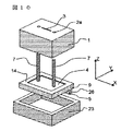
以下、本発明にかかわる実施の形態について図面を参照にして説明する。ただし図中の座標は、光素子の光軸方向をZ軸方向、2つのガイドピン穴に対して平行方向にX軸方向、垂直方向にY軸方向と定めて説明してゆく。 DESCRIPTION OF THE PREFERRED EMBODIMENTS Embodiments according to the present invention will be described below with reference to the drawings. However, the coordinates in the drawing will be described by defining the optical axis direction of the optical element as the Z-axis direction, the X-axis direction parallel to the two guide pin holes, and the Y-axis direction vertical.
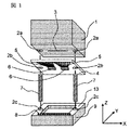
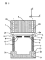
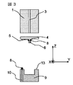
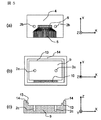
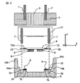
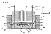
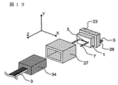
図1〜図3は第一の実施形態に係わる光モジュールを示しており、図1は斜視図であり、XYZ座標を図1内で描かれているように定めると、図2は光モジュール中央をXZ平面で切った断面図であり、図3はモジュール中央をYZ平面で切った断面図である。
この光モジュールはZ軸方向上方に光を出射する面型発光素子6とZ軸方向上方から光を受光する面型受光素子6を使用した光モジュールである。
1 to 3 show the optical module according to the first embodiment, FIG. 1 is a perspective view, and when XYZ coordinates are determined as shown in FIG. 1, FIG. 2 shows the center of the optical module. Is a cross-sectional view taken along the XZ plane, and FIG. 3 is a cross-sectional view taken along the YZ plane at the center of the module.
This optical module is an optical module using a surface
基板9上には凸部が設けられ、上面が透光性板用台座13となっている。基板9内にはモジュールから電気信号を入出力するスルーホール10が設けられている。半田8は透光性板4上の導電性パターン5の一部と基板9内のスルーホール10の一部が溶融接着され電気接続固定される目的のものである。基板9の凸部になっている透光性板用台座13は基板9と別体でも良く、材質も同一でなくて良い。
透光性板4上の導電性パターン5と光素子6の電極パッドは半田8によって電気的に接続される。
Convex portions are provided on the
The
ファイバブロック1にはファイバ3が固定保持されている。ファイバ3の本数が複数ファイバブロック1に固定される場合、このファイバ3同士のピッチは250μm程度が最も一般的である。
ファイバ3と光素子6の光学的接続は、ガイドピン7をガイド穴2a、2bに嵌合させることで、数μm程度の位置精度でなされている。更に透光板4上の導電性パターン5とスルーホール10の電気的接続もガイドピン7とガイド穴2b、2cを嵌合させることで数μm程度の精度でなされている。したがって、ガイドピン7とガイド穴2a、2b、2cは光学的接続と電気的接続の両方の機能を有している。
A fiber 3 is fixedly held on the
The optical connection between the fiber 3 and the
図1、2によると、ガイド穴2cは透光性板用台座13の面上に設けられているが、透光性板用台座13よりも基板9よりも低い部分に設けられていても良い。さらにガイド穴2cは基板9を貫通していても良い。
ガイドピン7は、ファイバブロック1、透光性板4、基板9のいずれかと一体化されても良い。更にガイドピン7はいずれかの部品に固着されていても良い。ガイドピン7は別の部品に固着しているか、作りつけられたものであっても良い。
1 and 2, the
The
ガイドピン7は基板9、透光性板4、ファイバブロック1を搭載する際に使用された後、抜いてもかまわない。その場合、搭載後はガイドピン7が無く、ガイド穴2が各部品に空いている光モジュールとなる。
透光性板4は光素子6に適した波長の少なくとも一部の光を透過する板であれば、レンズ、光フィルタ、偏光板、波長板、ミラー基板であっても良く、またその他の光学的性能を有するものであっても良い。
The guide pins 7 may be removed after being used when the
The
光素子6は多チャンネルのアレイ状光素子であっても良く、1チャンネル光素子であっても良い。また光ファイバ3が複数本ある場合、ファイバ3の一部の本数とだけ光結合をすることもある。図1において光素子6は二つ離間されて実装されており、光ファイバ3の中央付近の数本は光学的に使用されていない。更に光素子6が多チャンネルある場合には、実用上必要とされる光素子6だけ光ファイバ3と光学的結合が成されていても良い。
The
ファイバブロック1に固定されたファイバ3は光信号を導くものであればファイバ以外でも良く、このような用途としては石英、ポリマーを材料とした導波路が知られている。
更に、ファイバブロック1はモジュールから挿抜可能なものであっても良く、使用されるときのみ装着されていればよい。
The fiber 3 fixed to the
Furthermore, the
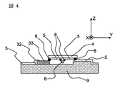
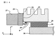
図4は第2の実施例に係わる光モジュールの一部であって、基板9と透光性板4の実装様態を示している。図4はモジュール中央部のYZ平面における断面図である。この光モジュールにおいては光素子6の電極パッドは半田8によって透光性板4上の導電性パターン5と電気接続が成されており、透光性板4上の導電性パターン5は半田8によって電子部品33の電極パッド及び基板9上の導電性パターン5と電気的接続がなされている。電子部品33の一部の電極パッドはワイヤ32を使って基板9上の導電性パターン5と電気的接続が成されている。
FIG. 4 is a part of an optical module according to the second embodiment, and shows a mounting state of the
電子部品33はコンデンサ素子、インダクタンス素子、LSI、IC等の他に導電性を有する部品で出来ていれば他のものでも良く、電気信号を基板9上の導電性パターン5やスルーホール10とやり取りするものである。
電子部品33の電極パッドと基板9上の導電性パターン5はワイヤ32以外にも半田、ペースト半田、導電性クリーム等の導電性の部材または接触により電気接続されても良い。
The electronic component 33 may be another component as long as it is made of a conductive component in addition to a capacitor element, an inductance element, an LSI, an IC, etc., and exchanges electrical signals with the
In addition to the wires 32, the electrode pads of the electronic component 33 and the
図4に示される基板9と透光性板4をガイドピン7とガイド穴2の嵌合によって位置あわせすると、透光性板4上の導電性パターン5と電子部品33の電極パッドは精度良く位置あわせされると共に基板9上の導電性パターンとも精度良く位置あわせされ電気的接続がなされる。
When the
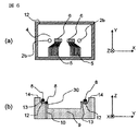
図5は第3の実施例に係わる光モジュールの一部であって、図5(a)は透光性板4のZ軸負方向から見た上面図、図5(b)はZ軸正方向から見た基板9の上面図、図5(c)は基板9中央部のYZ平面における断面図である。光素子6は多チャンネルのアレイ状光素子である。透光性板4は基板9上の透光性板用台座13に搭載される。透光性板4上の導電性パターン5は透光性板用台座13上面にあるスルーホール10の一部と電気的接続が成される。
5A and 5B show a part of the optical module according to the third embodiment. FIG. 5A is a top view of the
光部品を光部品用台座14上に搭載した際に、光部品が透光性板4に当らないように、光部品用台座14は透光性板用台座13よりもZ軸方向の高さが透光性板4の厚さ以上に高くなっている。したがって、図5に示される光モジュールでは、光部品用台座14を設けることで光部品搭載による衝撃や力を透光性板4に加わることを防ぐことが出来る構造を有している。
The
図6は第4の実施例に係わる光モジュールの一部であって、図6(a)は透光性板4のZ軸負方向から見た上面図、図6(b)は基板9中央部のYZ平面における断面図である。
透光性板4は基板9の透光性板用台座13に搭載されるが、透光性板4と透光性板用台座13上に金属薄膜12を付け、両者を半田8によって固着する。
6A and 6B show a part of the optical module according to the fourth embodiment. FIG. 6A is a top view of the
The
半田用台座30は透光性板用台座13よりZ軸方向に低くなる配置にあるが、これは金属薄膜12同士を半田8が隙間無く固着されることを助け固定を完全におこなうためである。
透光性板4と透光性板用台座13同士を固着する手段としては、半田、接着剤、樹脂、溶融金属、溶融ガラス等が有る。
The
Means for fixing the
図7は第5の実施例に係わる光モジュールの一部であって、図7(a)は透光性板4のZ軸負方向から見た上面図であり、図7(b)は基板9のZ軸正方向から見た上面図である。透光性板4上は光素子を取り囲むように金属薄膜12がついており、金属薄膜12はガイド穴2bの周囲にもついている。これより、この透光性板4上の金属薄膜12と透光性板用台座13上の金属薄膜12を半田8によって固着すると、光素子を外気から遮断した気密封止構造をとることが出来る。
半田8の代わりに樹脂、接着剤で透光性板4と透光性板用台座13を固定しても良い。
FIG. 7 shows a part of the optical module according to the fifth embodiment. FIG. 7A is a top view of the
Instead of the
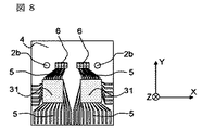
図8は第6の実施例に係わる光モジュールの一部であって、透光性板4のZ軸負方向から見た上面図である。透光性板4上の導電性パターン5と光素子6が電気接続されるように半田等によって搭載されると共に光素子駆動/電気信号増幅用のICも透光性板4上の導電性パターン5と電気接続が成されるように半田等によって搭載される。このように光素子6とIC31を同一の基板上に搭載することが可能になり、光素子6とIC31の距離は短くすることが出来るので、高周波電気信号の特性が良くなる。
透光性板4上にはIC31だけでなくそのほかの電子部品も搭載することが出来る。
FIG. 8 shows a part of the optical module according to the sixth embodiment, and is a top view of the
On the
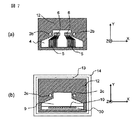
図9は第7の実施例に係わる光モジュールの実装途中を示す図であって、モジュール中央部のYZ平面における断面図である。ガイドピン7をガイド穴2b、2cに嵌合させることで、アレイレンズ基板11は基板9上の光部品台座14aに搭載され、透光性板4は基板9上の透光性板用台座13に搭載される。金属薄膜12上に置いた半田8を固着させることで、透光性板4は透光性板用台座13に固着されている。
FIG. 9 is a diagram showing the optical module according to the seventh embodiment while it is being mounted, and is a cross-sectional view in the YZ plane at the center of the module. By fitting the guide pins 7 into the guide holes 2 b and 2 c, the
ファイバブロック1は光部品用台座14bに搭載される。搭載時にファイバブロック1とアレイレンズ基板11があたらないように、光部品用台座14bと光部品用台座14aの高さの差はアレイレンズ基板11の厚さ以上である。アレイレンズ基板11とファイバ3との光結合はガイドピンを使わず行われている。これよりファイバブロック1に装着されている2本のガイドピン7と、レンズ基板11に装着されている2本のガイドピン7のY軸方向ピッチは異なったものとすることが出来る。
ファイバブロック1を光部品用台座14bに搭載することで、外気にある塵等はアレイレンズ基板11と基板9で囲まれた内部に混入することが無い。
The
By mounting the
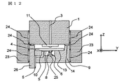
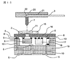
図10〜図12は第8の実施例に係わる光モジュールを示す図であって、図10は光モジュールの実装途中の斜視図、図11は光モジュール中央部のXZ平面における断面図、図12は光モジュール中央部のYZ平面における断面図である。ガイド穴2aとガイドピン7を嵌合させることによって、ファイバブロック1を光部品用台座14上に搭載する。
10 to 12 are views showing an optical module according to the eighth embodiment, in which FIG. 10 is a perspective view in the middle of mounting the optical module, FIG. 11 is a cross-sectional view in the XZ plane of the optical module central portion, and FIG. FIG. 3 is a cross-sectional view in the YZ plane of the optical module central portion. The
ファイバブロック1に固着されているアレイレンズ基板11はガイドピン7と嵌合するガイド穴を設けていない。
基板9に固着されている電気入出力用基板26上には導電性パターン5がパターニングされており、この導電性パターン5によってモジュールの電気信号入出力が行われる。接着ペースト24と光部品ガイド23は、ファイバブロック1と基板9の固定を強固にする効果を持っている。光素子6と基板9の間には放熱ペースト25が塗布してあり光素子から基板9への放熱を高めている。
The
A
図13は第8の実施例に係わる光モジュールに、光コネクタスリーブ27とガイド穴の開いたメス型の光コネクタ34を取り付けた斜視図である。光コネクタ34としてはMPO/MTコネクタ等の多芯光コネクタが知られ、光コネクタスリーブ27は光コネクタ34をガイド保持する機能を有する。
図10〜図13に示す光モジュールでは、コネクタ34の挿抜による衝撃と力はファイバブロック1に直接かかるが、それらの力は全て光部品ガイド23と光部品用台座14に保持され、透光性板4に力が加わることはないため、衝撃による透光性板4が壊れることは無い。
FIG. 13 is a perspective view in which an
In the optical module shown in FIGS. 10 to 13, the impact and force due to the insertion / extraction of the
更に図10〜図13に示す光モジュールでは、ファイバブロック1は基板9上の光部品用台座14に搭載されている。したがって、ファイバブロック1のZ軸上方からコネクタを挿抜することによる衝撃や力は、透光性板やアレイレンズ基板11に加わることは無い。またファイバブロックと光部品用台座14は接着ペーストによって固着されているので、外気の塵等はファイバブロック1と基板9で囲まれた内部には混入することはない。
Further, in the optical module shown in FIGS. 10 to 13, the
図14は第8の実施例に係わる光モジュールをX軸正方向から見た光モジュールであり、光コネクタスリーブ27、放熱フィン29、プリント回路基板28、電気コネクタ35が取り付けられている。光部品ガイド23に囲まれた基板9の裏面には放熱ペースト25が塗布されており、放熱フィン29がつけられている。したがって図14に示される光モジュールでは熱は放熱フィン29から空気中に放射される。
FIG. 14 shows an optical module in which the optical module according to the eighth embodiment is viewed from the positive direction of the X-axis, and has an
プリント回路基板28上には導電性パターンがパターニングされていてこの導電性パターンは電気入出力用基板26上の導電性パターン5と半田8によって電気的接続がなされている。外部基板36とプリント回路基板28と電気的接続は電気コネクタ35によって行われる。
図14に示される光モジュールは、光素子6や周辺の導電性パターン5、IC31等をXY平面に実装し、電気コネクタ35やプリント回路基板28をXZ平面に実装するので、Z軸方向の長さが小さい光モジュールを実現している。
A conductive pattern is patterned on the printed
The optical module shown in FIG. 14 has the
本発明を用いて作製された光モジュールは、特に面型受光/発光素子を用いた光モジュールに用いられ、電気信号から光信号、または逆に光信号から電気信号に変換する機能を持つ。これら光モジュールはルータ、伝送装置、コンピュータ、ディスプレイ、記憶装置、プリンタ等の装置に収められ、装置間を光信号で高速情報通信するためのものである。モジュール同士の光信号のやり取りはファイバを介してなされる。これらの点から、本発明は産業上の利用可能性を有する。 An optical module manufactured by using the present invention is used particularly for an optical module using a planar light-receiving / light-emitting element, and has a function of converting an electrical signal into an optical signal, or vice versa. These optical modules are housed in devices such as routers, transmission devices, computers, displays, storage devices, and printers, and are used for high-speed information communication between devices using optical signals. Optical signals are exchanged between modules through a fiber. From these points, the present invention has industrial applicability.
1 ファイバブロック
2 ガイド穴
3 ファイバ
4 透光性板
5 導電性パターン
6 光素子
7 ガイドピン
8 半田
9 基板
10 スルーホール
11 アレイレンズ基板
12 金属薄膜
13 透光性板用台座
14 光部品用台座
15 レンズホルダ
16 透明樹脂基板
17 コンデンサ
18 LSI
19 セラミック基板
20 光コネクタ
21 V溝
22 ミラー面
23 光部品ガイド
24 接着ペースト
25 放熱ペースト
26 電気入出力用基板
27 光コネクタスリーブ
28 高周波基板
29 放熱フィン
30 半田用台座
31 IC
32 ワイヤ
33 電子部品
34 光コネクタ
35 電気コネクタ
36 外部基板。
DESCRIPTION OF
19
32 Wire 33
Claims (9)
9. The optical module according to claim 8, wherein the guide hole or the guide pin for fitting the guide pin into the heat dissipation mechanism is attached.
Priority Applications (1)
| Application Number | Priority Date | Filing Date | Title |
|---|---|---|---|
| JP2004111688A JP2005292739A (en) | 2004-04-06 | 2004-04-06 | Optical module |
Applications Claiming Priority (1)
| Application Number | Priority Date | Filing Date | Title |
|---|---|---|---|
| JP2004111688A JP2005292739A (en) | 2004-04-06 | 2004-04-06 | Optical module |
Publications (1)
| Publication Number | Publication Date |
|---|---|
| JP2005292739A true JP2005292739A (en) | 2005-10-20 |
Family
ID=35325687
Family Applications (1)
| Application Number | Title | Priority Date | Filing Date |
|---|---|---|---|
| JP2004111688A Pending JP2005292739A (en) | 2004-04-06 | 2004-04-06 | Optical module |
Country Status (1)
| Country | Link |
|---|---|
| JP (1) | JP2005292739A (en) |
Cited By (14)
| Publication number | Priority date | Publication date | Assignee | Title |
|---|---|---|---|---|
| JP2007294743A (en) * | 2006-04-26 | 2007-11-08 | Hitachi Cable Ltd | Optical module and manufacturing method thereof |
| JP2007300032A (en) * | 2006-05-02 | 2007-11-15 | Hitachi Cable Ltd | Optical module and manufacturing method thereof |
| JP2007324303A (en) * | 2006-05-31 | 2007-12-13 | Hitachi Cable Ltd | Optical module and mounting method thereof |
| JP2008040318A (en) * | 2006-08-09 | 2008-02-21 | Hitachi Ltd | Manufacturing method of multi-channel optical module |
| WO2008023508A1 (en) * | 2006-08-22 | 2008-02-28 | Nec Corporation | Optical connector and optical coupling structure |
| JP2008134444A (en) * | 2006-11-28 | 2008-06-12 | Fujitsu Ltd | Optical module and optical waveguide structure |
| JP2009031455A (en) * | 2007-07-25 | 2009-02-12 | Fujikura Ltd | Circuit board heat dissipation structure with optical connector |
| JP2010016012A (en) * | 2008-06-30 | 2010-01-21 | Fujitsu Ltd | Photoelectric conversion device, photoelectric conversion module, and method of manufacturing photoelectric conversion device |
| US7960739B2 (en) | 2006-07-12 | 2011-06-14 | Hitachi Cable, Ltd. | Optical module and production method therefor |
| JP2013003177A (en) * | 2011-06-13 | 2013-01-07 | Sumitomo Electric Ind Ltd | Photoelectric conversion module and manufacturing method for the same |
| JP2014215499A (en) * | 2013-04-26 | 2014-11-17 | 株式会社フジクラ | Optical module |
| WO2018037551A1 (en) * | 2016-08-26 | 2018-03-01 | オリンパス株式会社 | Optical module for endoscope, endoscope, and method for manufacturing optical module for endoscope |
| JP2020030206A (en) * | 2018-08-13 | 2020-02-27 | コマツクス・ホールデイング・アー・ゲー | Inspection device for inspecting cable tip of cable and method for washing the same |
| US10905311B2 (en) | 2017-08-25 | 2021-02-02 | Olympus Corporation | Optical module for endoscope, endoscope, and manufacturing method for optical module for endoscope |
-
2004
- 2004-04-06 JP JP2004111688A patent/JP2005292739A/en active Pending
Cited By (18)
| Publication number | Priority date | Publication date | Assignee | Title |
|---|---|---|---|---|
| JP2007294743A (en) * | 2006-04-26 | 2007-11-08 | Hitachi Cable Ltd | Optical module and manufacturing method thereof |
| JP2007300032A (en) * | 2006-05-02 | 2007-11-15 | Hitachi Cable Ltd | Optical module and manufacturing method thereof |
| JP2007324303A (en) * | 2006-05-31 | 2007-12-13 | Hitachi Cable Ltd | Optical module and mounting method thereof |
| US7960739B2 (en) | 2006-07-12 | 2011-06-14 | Hitachi Cable, Ltd. | Optical module and production method therefor |
| JP2008040318A (en) * | 2006-08-09 | 2008-02-21 | Hitachi Ltd | Manufacturing method of multi-channel optical module |
| WO2008023508A1 (en) * | 2006-08-22 | 2008-02-28 | Nec Corporation | Optical connector and optical coupling structure |
| US8315491B2 (en) | 2006-08-22 | 2012-11-20 | Nec Corporation | Optical connector and optical coupling structure |
| JP2008134444A (en) * | 2006-11-28 | 2008-06-12 | Fujitsu Ltd | Optical module and optical waveguide structure |
| JP2009031455A (en) * | 2007-07-25 | 2009-02-12 | Fujikura Ltd | Circuit board heat dissipation structure with optical connector |
| JP2010016012A (en) * | 2008-06-30 | 2010-01-21 | Fujitsu Ltd | Photoelectric conversion device, photoelectric conversion module, and method of manufacturing photoelectric conversion device |
| JP2013003177A (en) * | 2011-06-13 | 2013-01-07 | Sumitomo Electric Ind Ltd | Photoelectric conversion module and manufacturing method for the same |
| JP2014215499A (en) * | 2013-04-26 | 2014-11-17 | 株式会社フジクラ | Optical module |
| WO2018037551A1 (en) * | 2016-08-26 | 2018-03-01 | オリンパス株式会社 | Optical module for endoscope, endoscope, and method for manufacturing optical module for endoscope |
| JPWO2018037551A1 (en) * | 2016-08-26 | 2019-06-20 | オリンパス株式会社 | Optical module for endoscope, endoscope, and method of manufacturing optical module for endoscope |
| US11445898B2 (en) | 2016-08-26 | 2022-09-20 | Olympus Corporation | Optical module for endoscope, endoscope, and manufacturing method for optical module for endoscope |
| US10905311B2 (en) | 2017-08-25 | 2021-02-02 | Olympus Corporation | Optical module for endoscope, endoscope, and manufacturing method for optical module for endoscope |
| JP2020030206A (en) * | 2018-08-13 | 2020-02-27 | コマツクス・ホールデイング・アー・ゲー | Inspection device for inspecting cable tip of cable and method for washing the same |
| JP7508205B2 (en) | 2018-08-13 | 2024-07-01 | コマツクス・ホールデイング・アー・ゲー | Inspection device for inspecting and cleaning the cable end of a cable - Patents.com |
Similar Documents
| Publication | Publication Date | Title |
|---|---|---|
| JP4825739B2 (en) | Structure of opto-electric hybrid board and opto-electric package | |
| US8867869B2 (en) | Miniaturized high speed optical module | |
| JP4477677B2 (en) | Optical module and manufacturing method thereof | |
| CN101911405B (en) | Optical module | |
| JP2007271998A (en) | Optical connector and optical module | |
| JP2008040318A (en) | Manufacturing method of multi-channel optical module | |
| JPWO2015001681A1 (en) | Optical module, optical module mounting method, optical module mounting circuit board, optical module evaluation kit system, circuit board, and communication system | |
| US9726826B2 (en) | Inter-lens adjusting method and photoelectric hybrid substrate | |
| JP2021139998A (en) | Optical module | |
| US20160043808A1 (en) | Optical transceiver | |
| JP2005292739A (en) | Optical module | |
| KR100627701B1 (en) | Parallel Optical Connection Module | |
| JP2015028658A (en) | Optical module, optical module mounting method, optical module mounting circuit board, optical module evaluation kit system, circuit board, and communication system | |
| CN114815093B (en) | Optical Module | |
| US10018791B2 (en) | Multi-channel optical subassembly and method of manufacturing the same | |
| US8750657B2 (en) | Flip-chip optical interface with micro-lens array | |
| US20250219350A1 (en) | Optical system-in-package, and optical module and optical transceiver using same | |
| JP2004286835A (en) | Optical element mounting apparatus, method of manufacturing the same, and wiring board with optical element mounting apparatus | |
| WO2015002520A1 (en) | Optical module having optical block for passive optical alignment and method for manufacturing same | |
| JP2011081343A (en) | Parallel optical communication device having weldable insert | |
| JPWO2009001822A1 (en) | Optical module | |
| JP2004288713A (en) | Manufacturing method of optical element mounting device | |
| CN114397734A (en) | A highly integrated vertical wireless light-emitting module | |
| KR20090124771A (en) | Photoelectric conversion module | |
| JP4739987B2 (en) | Optical fiber connection structure and optical fiber connection method |
Legal Events
| Date | Code | Title | Description |
|---|---|---|---|
| RD04 | Notification of resignation of power of attorney |
Free format text: JAPANESE INTERMEDIATE CODE: A7424 Effective date: 20060424 |
|
| A621 | Written request for application examination |
Free format text: JAPANESE INTERMEDIATE CODE: A621 Effective date: 20060830 |
|
| A977 | Report on retrieval |
Free format text: JAPANESE INTERMEDIATE CODE: A971007 Effective date: 20080822 |
|
| A131 | Notification of reasons for refusal |
Free format text: JAPANESE INTERMEDIATE CODE: A131 Effective date: 20080902 |
|
| A02 | Decision of refusal |
Free format text: JAPANESE INTERMEDIATE CODE: A02 Effective date: 20090106 |