JP2009145822A - Image display apparatus - Google Patents
Image display apparatus Download PDFInfo
- Publication number
- JP2009145822A JP2009145822A JP2007325803A JP2007325803A JP2009145822A JP 2009145822 A JP2009145822 A JP 2009145822A JP 2007325803 A JP2007325803 A JP 2007325803A JP 2007325803 A JP2007325803 A JP 2007325803A JP 2009145822 A JP2009145822 A JP 2009145822A
- Authority
- JP
- Japan
- Prior art keywords
- substrate
- image display
- envelope
- substrates
- display device
- Prior art date
- Legal status (The legal status is an assumption and is not a legal conclusion. Google has not performed a legal analysis and makes no representation as to the accuracy of the status listed.)
- Withdrawn
Links
Images


Classifications
-
- H—ELECTRICITY
- H01—ELECTRIC ELEMENTS
- H01J—ELECTRIC DISCHARGE TUBES OR DISCHARGE LAMPS
- H01J9/00—Apparatus or processes specially adapted for the manufacture, installation, removal, maintenance of electric discharge tubes, discharge lamps, or parts thereof; Recovery of material from discharge tubes or lamps
- H01J9/24—Manufacture or joining of vessels, leading-in conductors or bases
- H01J9/26—Sealing together parts of vessels
- H01J9/261—Sealing together parts of vessels the vessel being for a flat panel display
-
- H—ELECTRICITY
- H01—ELECTRIC ELEMENTS
- H01J—ELECTRIC DISCHARGE TUBES OR DISCHARGE LAMPS
- H01J29/00—Details of cathode-ray tubes or of electron-beam tubes of the types covered by group H01J31/00
- H01J29/02—Electrodes; Screens; Mounting, supporting, spacing or insulating thereof
- H01J29/10—Screens on or from which an image or pattern is formed, picked up, converted or stored
- H01J29/16—Incandescent screens
-
- H—ELECTRICITY
- H01—ELECTRIC ELEMENTS
- H01J—ELECTRIC DISCHARGE TUBES OR DISCHARGE LAMPS
- H01J31/00—Cathode ray tubes; Electron beam tubes
- H01J31/08—Cathode ray tubes; Electron beam tubes having a screen on or from which an image or pattern is formed, picked up, converted, or stored
- H01J31/10—Image or pattern display tubes, i.e. having electrical input and optical output; Flying-spot tubes for scanning purposes
- H01J31/12—Image or pattern display tubes, i.e. having electrical input and optical output; Flying-spot tubes for scanning purposes with luminescent screen
- H01J31/123—Flat display tubes
- H01J31/125—Flat display tubes provided with control means permitting the electron beam to reach selected parts of the screen, e.g. digital selection
- H01J31/127—Flat display tubes provided with control means permitting the electron beam to reach selected parts of the screen, e.g. digital selection using large area or array sources, i.e. essentially a source for each pixel group
Abstract
Description
本発明は画像表示装置に関し、特に、画像表示装置の基板同士の接合構造に関する。 The present invention relates to an image display device, and more particularly to a bonding structure between substrates of an image display device.
表面伝導型電子放出素子や電界放出型電子放出素子を用いた画像表示装置が知られている。この種の画像表示装置では、画像表示部が形成された基板と、電子放出源が形成された基板とが対向して配置され、これらの基板が外枠を介して接合される構造が一般的である。具体的には、基板の一方に外枠がフリット(低融点ガラス)で強固に固定され、外枠と基板の他方とが接合材でシールされ、外囲器が形成される。接合材としては、In(インジウム)等の低融点金属が用いられる。基板の間、すなわち外囲器の内部は真空の空間となっており、内部の空間は接合材によって外部からシールされる。 2. Description of the Related Art Image display devices using surface conduction electron-emitting devices and field emission electron-emitting devices are known. In this type of image display apparatus, a structure in which a substrate on which an image display unit is formed and a substrate on which an electron emission source is formed is arranged to face each other, and these substrates are joined via an outer frame. It is. Specifically, the outer frame is firmly fixed to one side of the substrate with a frit (low melting point glass), and the outer frame and the other side of the substrate are sealed with a bonding material to form an envelope. As the bonding material, a low melting point metal such as In (indium) is used. The space between the substrates, that is, the inside of the envelope is a vacuum space, and the internal space is sealed from the outside by a bonding material.
通常、各基板はガラスを基材として形成されるが、使用時の温度差などの要因により、各基板には基板間の熱膨張の差に起因する歪が生じることがある。この歪によって、基板同士が相対的な位置ずれを起こすと、電子源から放出される電子ビームが画像表示部の所望の位置からずれた位置に照射され、画質の低下を招くおそれがある。そこで、特許文献1には、接合材でシールされた外囲器の外側に、シリカ・アルミナを主成分とする無機接着剤などからなる補強構造を有する構成が開示されている。接着剤(補強構造)は両基板の間にディスペンサー等を用いて形成され、両基板を強固に固定する。これによって、熱膨張の差に起因する基板同士の位置ずれが防止される。
特許文献1に開示されている補強構造は基板同士の位置ずれを防止するためには有効であるが、基板が相互に拘束されるため、基板に熱膨張の差に起因する歪が生じる場合がある。基板に歪が生じると基板同士の位置ずれを防止しても、基板自身の健全性に影響を与え、画像表示装置としての信頼性を低下させるおそれがある。
Although the reinforcement structure disclosed in
そこで、本発明は、基板同士の位置ずれ防止と基板に生じる歪の抑制の双方を実現することのできる画像表示装置を提供することを目的とする。 SUMMARY OF THE INVENTION An object of the present invention is to provide an image display apparatus that can realize both prevention of positional deviation between substrates and suppression of distortion generated in the substrates.
本発明の画像表示装置は、画像表示部を備えた第1の基板と、第1の基板と対向して位置する第2の基板と、第1の基板と該第2の基板とを、間に空間を設けて気密に接合する接合部材と、を含む外囲器を有している。本発明の画像表示装置はさらに、外囲器の外周の一部に沿って位置し、第1の基板と第2の基板の双方に接して設けられ、第1の基板と第2の基板との位置ずれを抑制する位置ずれ抑制部材を有している。 An image display device of the present invention includes a first substrate having an image display unit, a second substrate positioned opposite to the first substrate, the first substrate, and the second substrate. And a bonding member that is hermetically bonded by providing a space. The image display device of the present invention is further located along a part of the outer periphery of the envelope, is provided in contact with both the first substrate and the second substrate, and includes the first substrate and the second substrate. A positional deviation suppressing member that suppresses the positional deviation.
このように構成された画像表示装置は、位置ずれ抑制部材が接合部材の外周の一部に沿って位置しているため、位置ずれ抑制部材による位置ずれ抑制効果を維持しつつ、第1の基板と第2の基板との拘束が抑えられ、基板に生じる歪が抑制される。 In the image display device configured as described above, since the misalignment suppressing member is located along a part of the outer periphery of the joining member, the first substrate is maintained while maintaining the misalignment suppressing effect of the misalignment suppressing member. And the second substrate are restrained, and distortion generated in the substrate is restrained.
本発明の画像表示装置は、画像表示部を備えた第1の基板と、第1の基板と対向して位置する第2の基板と、第1の基板と第2の基板とを、間に空間を設けて気密に接合する接合部材と、を含む外囲器を備えた画像表示装置に広く適用することができる。このような画像表示装置には、液晶画像表示装置、プラズマ画像表示装置、電子線画像表示装置などが含まれる。なお、第1の基板と第2の基板とを気密に接合するとは、第1の基板と第2の基板とを直接接合することは勿論、第1の基板と第2の基板とを外枠を介して接合することも含んでいる。液晶画像表示装置や電子線画像表示装置は2つの基板を周縁部で接合しているため、本発明が適用される好ましい形態である。 An image display device according to the present invention includes a first substrate provided with an image display unit, a second substrate positioned opposite to the first substrate, and the first substrate and the second substrate. The present invention can be widely applied to an image display device including an envelope including a bonding member that provides a space and is airtightly bonded. Such image display devices include liquid crystal image display devices, plasma image display devices, electron beam image display devices, and the like. Note that airtightly bonding the first substrate and the second substrate means that the first substrate and the second substrate are directly bonded together, as well as the first substrate and the second substrate. It also includes joining via. A liquid crystal image display device or an electron beam image display device is a preferable embodiment to which the present invention is applied because two substrates are joined at the peripheral edge.
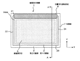
(第1の実施形態)図1,2は各々、本発明の第1の実施形態を示す画像表示装置の正面図と、第1図のA−A’線に沿った断面図である。第1の実施形態は表面伝導型電子放出素子を用いた画像表示装置である。 (First Embodiment) FIGS. 1 and 2 are a front view of an image display apparatus showing a first embodiment of the present invention and a cross-sectional view taken along the line A-A 'of FIG. The first embodiment is an image display device using a surface conduction electron-emitting device.
第1の基板2は蛍光体層(図示せず)等からなる画像表示部5を備えている。第2の基板3は電子放出源(図示せず)を備え、第1の基板2と対向して位置して設けられている。電子放出源からは画像信号に応じて電子が放出され、蛍光体層に衝突し、蛍光体層が発光して、所望の画像が表示される。第1の基板2と第2の基板3との間には空間8が設けられている。第1の基板2と第2の基板3は外枠4を介して接合され、内部が真空にされた外囲器7を構成している。第1の基板2及び第2の基板3は概ね矩形の基板であり、従って、外囲器7も概ね矩形形状を有している。
The
第2の基板3と外枠4とはフリット11によって強固に接合されている。第1の基板2と外枠4とは接合部材12によって接合されている。接合部材12はInやInAg合金等の低融点金属を用いることができる。接合部材12は第2の基板3と外枠4とを気密に接合し、外囲器7の内部を外囲器7の外部からシールする。
The
外囲器7の外周の一部に沿って、位置ずれ抑制部材6が設けられている。位置ずれ抑制部材6としては、エポキシ系接着剤、アクリル系接着剤、セラミック系接着剤などを用いることができ、特にエポキシ系接着剤が機械的強度及び作業性から好ましい。位置ずれ抑制部材6は金属部材やガラス部材で構成してもよい。位置ずれ抑制部材6は本実施形態では外枠4と接して設けられているが、外枠4から離れて設けられていても構わない。すなわち、外枠4と位置ずれ抑制部材6との間に空間が設けられていても構わない。位置ずれ抑制部材6は第1の基板2と第2の基板3の双方に接するように設けられ、第1の基板2と第2の基板3との位置ずれを抑制する。位置ずれは、クリープによる変形が生じやすい低融点金属を接合部材12として用いた場合に顕著になりやすいが、本実施形態はこのような外囲器に対して特に効果的である。
A
位置ずれ抑制部材6は、外囲器7の辺21のみに沿って設けられている。勿論、外囲器7の辺22,23,24のいずれかのみに沿って設けられていても構わない。これによって、第1の基板2と第2の基板3の相対的な位置ずれを実用上十分に防止することができる。また、基板2,3は辺21のみでしか拘束されていないため、位置ずれ抑制部材6は、図1のY方向に対して拘束効果を発生させることがなく、X方向についても、拘束力は限定されたものとなる。一辺だけに位置ずれ抑制部材6を設けることは、位置ずれ抑制部材6の設置範囲も限定されるため、部材コストおよびプロセスタクトの観点からも好ましい。
The
位置ずれ抑制部材6は、外囲器7の辺21,22,23,24のうち最大3辺までに設けることができる。このように、位置ずれ抑制部材6を少なくとも一辺を除いて設けることにより(本実施形態では一辺のみに設けることにより)、基板2,3の相対的な位置ずれを問題にならない程度に維持しながら、基板2,3の熱膨張差に起因する基板2,3の歪みを抑制できる。従って、基板2,3等の破損を防止しながら、基板2,3の相対位置関係を正常な範囲に保つことが可能となる。第1の基板2と第2の基板3の位置ずれは、各基板2,3のゆがみや、接着時の変形など製造プロセスに起因する残留応力や、熱膨張率の違いによる使用時の温度変化によって発生する。従って、位置ずれ抑制部材6の設置範囲は、これらの残留応力、温度変化等の大小に応じて適宜決めることが好ましい。ただし、上述したように、一般的には、位置ずれ抑制部材6は一辺のみに設けることが好ましい。
The positional
本実施形態の画像表示装置は概略以下のようにして製造することができる。第1の基板2と表面伝導型電子放出素子(図示せず)を搭載した第2の基板3とを準備し、これらの周縁部に枠4を挟み込んで、フリット11及び接合部材12を用いて接着する。接着後、不図示の排気穴から排気し、排気穴を封止することで外囲器7を作製する。次に、外囲器7を作製後、外囲器7の姿勢を水平に保ちながら、ディスペンサーにて位置ずれ抑制部材6(接着剤)を塗布し、自然乾燥により硬化させる。このようにして製造された画像表示装置は良好な画像を表示することができた。
The image display apparatus of the present embodiment can be manufactured generally as follows. A
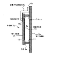
(第2の実施形態)図3,4は各々、本発明の第2の実施形態を示す画像表示装置の正面図と、第3図のB−B’線に沿った断面図である。第2の実施形態は電界放出型素子を用いた画像表示装置であるが、表面伝導型電子放出素子を用いた画像表示装置、あるいは液晶画像表示装置等、他の画像表示装置にも同様に適用できる。第2の実施形態はこの点の他、位置ずれ抑制部材の構成及び設置方法が第1の実施形態と異なっていることを除き、第1の実施形態と同様である。 (Second Embodiment) FIGS. 3 and 4 are respectively a front view of an image display device showing a second embodiment of the present invention and a cross-sectional view taken along the line B-B 'of FIG. The second embodiment is an image display device using a field emission device, but is similarly applied to other image display devices such as an image display device using a surface conduction electron-emitting device or a liquid crystal image display device. it can. In addition to this point, the second embodiment is the same as the first embodiment except that the configuration and installation method of the misregistration suppressing member are different from those of the first embodiment.
本実施形態では、位置ずれ抑制部材6a,6bは、外囲器7aの互いに隣接する2辺21a,24aの一部のみに、第1の基板2aと第2の基板3aを連結する様に設けられている。位置ずれ抑制部材6a,6bはFe−47Ni合金からなる金属部材であり、これをセラミック系接着剤16aを用いて基板2a,3aに接着している。Fe−47Ni合金は、その熱膨張率が第1の基板2aの熱膨張率と第2の基板3aの熱膨張率の双方に近いため、基板2a,3aとの接着面で熱応力が発生しにくい。従って、基板2a,3aが局部的に大きな歪を受けることが防止される。
In the present embodiment, the
位置ずれ抑制部材は本実施形態では、外囲器7aの隣接する辺に2つ(位置ずれ抑制部材6a,6b)設けられているが、第1の実施形態と同様、いずれか一辺の一部だけに設けられていてもよいし、隣接する3辺、あるいは対向する2辺に設けられていてもよい。ただし、個々の位置ずれ抑制部材の位置ずれ抑制効果は第1の実施形態の位置ずれ抑制部材6に比べて小さいので、本実施形態では隣接する辺に合計2つ設けている。また、位置ずれ抑制部材6a,6bの大きさ(範囲)は図示の通りである必要はなく、各基板2,3のゆがみや、接着時の変形などに起因する残留応力や、熱膨張率の違いによる使用時の温度変化等を考慮して適宜に設定することができる。各辺に取り付ける位置ずれ抑制部材の個数も1個に限定されず、上記条件を考慮の上、許容できる範囲の熱応力に収まるように、複数に分割することもできる。
In the present embodiment, two misregistration suppression members are provided on adjacent sides of the envelope 7a (the
位置ずれ抑制部材6a,6bは、位置ずれ抑制部材6a,6bが設けられている辺21a,24aの中央部に位置している。この結果、第1の基板2aと第2の基板3aとが外囲器7aの辺21a,24aの中央部で固定され、位置ずれは辺21a,24aの中央部を中心として発生し、歪も中央部を中心として発生する。従って、第1の基板2aと第2の基板3aとを外囲器7aの隅部で固定する場合と比べ、位置ずれ量、歪の大きさとも半分に抑制できる。これにより、位置ずれに起因する色ずれなどを低減することも可能となる。
The
本実施形態の画像表示装置も概ね第1の実施形態と同様に製作できる。第1の実施形態と同様にして外囲器7aを製造した後、外囲器7aの姿勢を水平に保ち、ディスペンサーを用いて接着面に接着剤16aが塗布された位置ずれ抑制部材6a,6bを基板2a,3aの接合面に押付け、加圧しながら自然乾燥により硬化させる。一例では、位置ずれ抑制部材6a,6bと、第1の基板2aおよび第2の基板3aとの接着面積は、それぞれ500mm2とした。このようにして製造された画像表示装置は良好な画像を表示することができた。
The image display device of this embodiment can also be manufactured in substantially the same manner as in the first embodiment. After manufacturing the envelope 7a in the same manner as in the first embodiment, the position of the envelope 7a is kept horizontal, and the positional
1,1a 画像表示装置
2,2a 第1の基板
3,3a 第2の基板
4,4a 外枠
5,5a 画像表示部
6,6a,6b 位置ずれ抑制部材
7,7a 外囲器
8,8a 空間
12 接合部材
DESCRIPTION OF
Claims (6)
前記外囲器の外周の一部に沿って位置し、前記第1の基板と前記第2の基板の双方に接して設けられ、前記第1の基板と前記第2の基板との位置ずれを抑制する位置ずれ抑制部材と、
を有する、画像表示装置。 A first substrate provided with an image display unit, a second substrate positioned opposite to the first substrate, and the first substrate and the second substrate are airtight with a space between them. An envelope including a bonding member bonded to
It is located along a part of the outer periphery of the envelope, is provided in contact with both the first substrate and the second substrate, and the positional deviation between the first substrate and the second substrate is adjusted. A misregistration suppressing member for suppressing,
An image display device.
Priority Applications (4)
| Application Number | Priority Date | Filing Date | Title |
|---|---|---|---|
| JP2007325803A JP2009145822A (en) | 2007-12-18 | 2007-12-18 | Image display apparatus |
| US12/273,910 US7817221B2 (en) | 2007-12-18 | 2008-11-19 | Image display apparatus |
| EP08170616A EP2073244A3 (en) | 2007-12-18 | 2008-12-03 | Image display apparatus |
| CN2008101852075A CN101465257B (en) | 2007-12-18 | 2008-12-18 | Image display apparatus |
Applications Claiming Priority (1)
| Application Number | Priority Date | Filing Date | Title |
|---|---|---|---|
| JP2007325803A JP2009145822A (en) | 2007-12-18 | 2007-12-18 | Image display apparatus |
Publications (2)
| Publication Number | Publication Date |
|---|---|
| JP2009145822A true JP2009145822A (en) | 2009-07-02 |
| JP2009145822A5 JP2009145822A5 (en) | 2010-08-05 |
Family
ID=40433849
Family Applications (1)
| Application Number | Title | Priority Date | Filing Date |
|---|---|---|---|
| JP2007325803A Withdrawn JP2009145822A (en) | 2007-12-18 | 2007-12-18 | Image display apparatus |
Country Status (4)
| Country | Link |
|---|---|
| US (1) | US7817221B2 (en) |
| EP (1) | EP2073244A3 (en) |
| JP (1) | JP2009145822A (en) |
| CN (1) | CN101465257B (en) |
Families Citing this family (4)
| Publication number | Priority date | Publication date | Assignee | Title |
|---|---|---|---|---|
| JP2009145822A (en) * | 2007-12-18 | 2009-07-02 | Canon Inc | Image display apparatus |
| JP2009216889A (en) * | 2008-03-10 | 2009-09-24 | Canon Inc | Display apparatus |
| JP2010267541A (en) * | 2009-05-15 | 2010-11-25 | Canon Inc | Display panel and image display apparatus |
| JP2012003060A (en) | 2010-06-17 | 2012-01-05 | Canon Inc | Image display device, holding member thereof, and image display system |
Family Cites Families (18)
| Publication number | Priority date | Publication date | Assignee | Title |
|---|---|---|---|---|
| US5016987A (en) * | 1990-06-05 | 1991-05-21 | Hughes Aircraft Company | Liquid crystal cell sealant assembly |
| US6506087B1 (en) * | 1998-05-01 | 2003-01-14 | Canon Kabushiki Kaisha | Method and manufacturing an image forming apparatus having improved spacers |
| US6848964B1 (en) * | 1998-09-14 | 2005-02-01 | Matsushita Electric Industrial Co., Ltd. | Sealing method and apparatus for manufacturing high-performance gas discharge panel |
| JP2000090830A (en) | 1998-09-17 | 2000-03-31 | Canon Inc | Manufacture for image display device |
| JP2000090829A (en) | 1998-09-17 | 2000-03-31 | Canon Inc | Manufacture for image display device |
| JP2000251807A (en) | 1999-03-02 | 2000-09-14 | Canon Inc | Image forming device and its manufacture |
| US6361389B1 (en) * | 1999-09-30 | 2002-03-26 | Honeywell International Inc. | Substrate coupling method |
| JP3560587B2 (en) * | 2001-01-25 | 2004-09-02 | ランテクニカルサービス株式会社 | Display panel substrate bonding method and apparatus |
| JP2002343282A (en) | 2001-05-17 | 2002-11-29 | Toshiba Corp | Image display unit |
| CN1213389C (en) | 2001-08-31 | 2005-08-03 | 佳能株式会社 | Image display device and producing method thereof |
| US7029358B2 (en) * | 2002-06-28 | 2006-04-18 | Canon Kabushiki Kaisha | Hermetic container and image display apparatus using the same |
| JP3754969B2 (en) | 2002-06-28 | 2006-03-15 | キヤノン株式会社 | Airtight container and image display apparatus using the same |
| US20050140913A1 (en) * | 2002-08-29 | 2005-06-30 | Masahiro Yokota | Flat display device |
| JP4035494B2 (en) | 2003-09-10 | 2008-01-23 | キヤノン株式会社 | Airtight container and image display device using the same |
| JP4557781B2 (en) * | 2005-04-07 | 2010-10-06 | キヤノン株式会社 | Image display device |
| US20070188757A1 (en) * | 2006-02-14 | 2007-08-16 | Jeffrey Michael Amsden | Method of sealing a glass envelope |
| KR100879296B1 (en) * | 2006-04-20 | 2009-01-16 | 삼성에스디아이 주식회사 | Vacuum envelop for display device, manufacturing method of the vacuum envelop, and electron emission display device using the same |
| JP2009145822A (en) * | 2007-12-18 | 2009-07-02 | Canon Inc | Image display apparatus |
-
2007
- 2007-12-18 JP JP2007325803A patent/JP2009145822A/en not_active Withdrawn
-
2008
- 2008-11-19 US US12/273,910 patent/US7817221B2/en not_active Expired - Fee Related
- 2008-12-03 EP EP08170616A patent/EP2073244A3/en not_active Withdrawn
- 2008-12-18 CN CN2008101852075A patent/CN101465257B/en not_active Expired - Fee Related
Also Published As
| Publication number | Publication date |
|---|---|
| EP2073244A2 (en) | 2009-06-24 |
| US20090154077A1 (en) | 2009-06-18 |
| US7817221B2 (en) | 2010-10-19 |
| CN101465257B (en) | 2011-04-20 |
| CN101465257A (en) | 2009-06-24 |
| EP2073244A3 (en) | 2010-03-24 |
Similar Documents
| Publication | Publication Date | Title |
|---|---|---|
| US7659554B2 (en) | Hermetic container and image display apparatus | |
| KR20050077751A (en) | Container for flat panel display, and flat panel display using the same | |
| KR20110109930A (en) | Manufacturing method of hermetic container | |
| JP2009145822A (en) | Image display apparatus | |
| US20070200476A1 (en) | Display device | |
| US7501751B2 (en) | Display device and method of manufacturing same | |
| KR20020020188A (en) | A sealing vessel, method for manufacturing thereof and a display apparatus using such sealing vessel | |
| US7029358B2 (en) | Hermetic container and image display apparatus using the same | |
| KR20060043544A (en) | Display device | |
| JP5627370B2 (en) | Depressurized airtight container and image display device manufacturing method | |
| JP2009199758A (en) | Airtight vessel, and image display device using the same | |
| TWI270917B (en) | Image display device and the manufacturing method thereof | |
| JP2010073413A (en) | Method of making vacuum container | |
| JP2005332730A (en) | Display device, display module, and display panel | |
| JP2005302565A (en) | Flat image display device | |
| JP2003132823A (en) | Panel display device and manufacturing method therefor | |
| JP2007309959A (en) | Reinforcing structure for display panel | |
| US20070029923A1 (en) | Display panel | |
| JP2007207436A (en) | Image display device and its manufacturing method | |
| JP2007311031A (en) | Reinforcement for display panel, and mounting method of reinforcement | |
| JP2007324040A (en) | Flat display device, its manufacturing method, and sealing frame | |
| JP2007188784A (en) | Image display device and manufacturing method thereof | |
| JPH02281540A (en) | Vacuum container for flat image display | |
| JP2007234400A (en) | Image display device | |
| JPH10208668A (en) | Image display device |
Legal Events
| Date | Code | Title | Description |
|---|---|---|---|
| A521 | Request for written amendment filed |
Free format text: JAPANESE INTERMEDIATE CODE: A523 Effective date: 20100617 |
|
| A621 | Written request for application examination |
Free format text: JAPANESE INTERMEDIATE CODE: A621 Effective date: 20100617 |
|
| A761 | Written withdrawal of application |
Free format text: JAPANESE INTERMEDIATE CODE: A761 Effective date: 20110616 |