JP4557781B2 - Image display device - Google Patents
Image display device Download PDFInfo
- Publication number
- JP4557781B2 JP4557781B2 JP2005110707A JP2005110707A JP4557781B2 JP 4557781 B2 JP4557781 B2 JP 4557781B2 JP 2005110707 A JP2005110707 A JP 2005110707A JP 2005110707 A JP2005110707 A JP 2005110707A JP 4557781 B2 JP4557781 B2 JP 4557781B2
- Authority
- JP
- Japan
- Prior art keywords
- anode
- display panel
- anode terminal
- image display
- cap
- Prior art date
- Legal status (The legal status is an assumption and is not a legal conclusion. Google has not performed a legal analysis and makes no representation as to the accuracy of the status listed.)
- Expired - Fee Related
Links
Images


Classifications
-
- H—ELECTRICITY
- H01—ELECTRIC ELEMENTS
- H01R—ELECTRICALLY-CONDUCTIVE CONNECTIONS; STRUCTURAL ASSOCIATIONS OF A PLURALITY OF MUTUALLY-INSULATED ELECTRICAL CONNECTING ELEMENTS; COUPLING DEVICES; CURRENT COLLECTORS
- H01R13/00—Details of coupling devices of the kinds covered by groups H01R12/70 or H01R24/00 - H01R33/00
- H01R13/46—Bases; Cases
- H01R13/53—Bases or cases for heavy duty; Bases or cases for high voltage with means for preventing corona or arcing
-
- H—ELECTRICITY
- H01—ELECTRIC ELEMENTS
- H01R—ELECTRICALLY-CONDUCTIVE CONNECTIONS; STRUCTURAL ASSOCIATIONS OF A PLURALITY OF MUTUALLY-INSULATED ELECTRICAL CONNECTING ELEMENTS; COUPLING DEVICES; CURRENT COLLECTORS
- H01R13/00—Details of coupling devices of the kinds covered by groups H01R12/70 or H01R24/00 - H01R33/00
- H01R13/62—Means for facilitating engagement or disengagement of coupling parts or for holding them in engagement
- H01R13/627—Snap or like fastening
- H01R13/6277—Snap or like fastening comprising annular latching means, e.g. ring snapping in an annular groove
-
- H—ELECTRICITY
- H01—ELECTRIC ELEMENTS
- H01R—ELECTRICALLY-CONDUCTIVE CONNECTIONS; STRUCTURAL ASSOCIATIONS OF A PLURALITY OF MUTUALLY-INSULATED ELECTRICAL CONNECTING ELEMENTS; COUPLING DEVICES; CURRENT COLLECTORS
- H01R13/00—Details of coupling devices of the kinds covered by groups H01R12/70 or H01R24/00 - H01R33/00
- H01R13/02—Contact members
- H01R13/10—Sockets for co-operation with pins or blades
- H01R13/11—Resilient sockets
- H01R13/111—Resilient sockets co-operating with pins having a circular transverse section
Description
本発明は、表示パネルのアノード端子に導電線を接続するためのアノードキャップと、該アノードキャップを用いた電圧供給ユニット、さらには、該ユニットを備えた画像表示装置に関する。 The present invention relates to an anode cap for connecting a conductive line to an anode terminal of a display panel, a voltage supply unit using the anode cap, and an image display device including the unit.
従来、テレビジョン受像機の陰極線管におけるアノード電圧の供給は、陰極線管の外面に設けられたいわゆるアノード釦に、高電圧源と接続された導電線を電気的に接続することでなされており、この電気的な接続は、前記導電線の遊端に設けられたアノード釦係合用片部をアノード釦に挿入し、固定することでなされていた(特許文献1参照)。 Conventionally, the supply of the anode voltage in the cathode ray tube of a television receiver has been made by electrically connecting a conductive line connected to a high voltage source to a so-called anode button provided on the outer surface of the cathode ray tube. This electrical connection has been made by inserting and fixing an anode button engagement piece provided at the free end of the conductive wire into the anode button (see Patent Document 1).
特許文献1の図10に示されるように、アノード釦は陰極線管を構成する外壁に埋設されているため、アノード釦係合用片部の着脱時に外壁のアノード釦埋設部分に応力が集中する。平面型表示パネルにおいては、パネルが薄いガラス基板で構成されているため、このような埋設して用いるアノード釦を用いた場合、着脱時にかかる応力によって基板の破損を招く恐れがある。 As shown in FIG. 10 of Patent Document 1, since the anode button is embedded in the outer wall constituting the cathode ray tube, stress concentrates on the anode button embedded portion of the outer wall when the anode button engaging piece is attached or detached. In a flat display panel, since the panel is formed of a thin glass substrate, when such an embedded anode button is used, the substrate may be damaged due to stress applied during attachment / detachment.
本発明は、平面型や陰極線管などの表示パネルにおいて、アノード端子とこれに電圧を供給する導電線との良好な電気的接続が得られると同時に、該導電線の着脱が可能で、かつ、着脱時に表示パネルにかかる応力を緩和して、着脱時の表示パネルの損傷を防止することにある。 In a display panel such as a flat type or a cathode ray tube, the present invention provides a good electrical connection between an anode terminal and a conductive line supplying voltage to the anode terminal, and the conductive line can be attached and detached. The object is to relieve the stress applied to the display panel during attachment and detachment and prevent damage to the display panel during attachment and detachment.
本発明は、少なくともアノード電極とアノード端子とを備えた表示パネルと、前記アノード端子に電圧を供給するための導電線を保持するアノードキャップと、前記アノードキャップを着脱可能に係止する部材と、を有する画像表示装置であって、
前記アノード電極は前記表示パネルの内部に設けられており、
前記アノード端子は前記アノード電極に前記表示パネルの外側から電圧を供給するための端子であって、前記表示パネルの内部に位置する部分と前記表示パネルの外部に位置する部分とを備えており、
前記部材は、前記アノード端子の、前記表示パネルの外部に位置する部分が挿入された貫通孔を備えており、且つ、前記表示パネルの外表面に固定されており、
前記アノードキャップは、弾性素材で構成された椀状のカバー部を有し、該カバー部の端部が前記部材の周囲の前記表示パネル外表面に弾性的に押し付けられた状態で前記部材によって係止される係止部を前記カバー部の内側に有することを特徴とする。
The present invention includes a display panel including at least an anode electrode and an anode terminal, an anode cap that holds a conductive line for supplying a voltage to the anode terminal, and a member that detachably locks the anode cap; An image display device comprising:
The anode electrode is provided inside the display panel,
The anode terminal is a terminal for supplying a voltage to the anode electrode from the outside of the display panel, and includes a portion located inside the display panel and a portion located outside the display panel,
The member includes a through-hole into which a portion of the anode terminal located outside the display panel is inserted, and is fixed to the outer surface of the display panel,
The anode cap has a bowl-shaped cover portion made of an elastic material, and the end portion of the cover portion is engaged with the member in a state of being elastically pressed against the outer surface of the display panel around the member. It has a latching | locking part stopped inside the said cover part, It is characterized by the above-mentioned .
本発明によれば、電圧供給ユニットを表示パネルから着脱する際の応力のほとんどが弾性部材であるアノードキャップにかかるため、該ユニットの着脱時の表示パネルの損傷が防止される。 According to the present invention, most of the stress when the voltage supply unit is attached to and detached from the display panel is applied to the anode cap, which is an elastic member, so that the display panel is prevented from being damaged when the unit is attached and detached.
図1に、本発明のアノードキャップの好ましい一実施形態の断面模式図を、図2に、該アノードキャップを用いた本発明の電圧供給ユニットの好ましい一実施形態の断面模式図を、図3に、図2の電圧供給ユニットを装着する表示パネルのアノード端子周辺の断面模式図を、図4に、図3の固定部材と図2の電圧供給ユニットを備えた本発明の画像表示装置の一実施形態の表示パネルの断面模式図を示す。 1 is a schematic cross-sectional view of a preferred embodiment of the anode cap of the present invention, FIG. 2 is a schematic cross-sectional view of a preferred embodiment of the voltage supply unit of the present invention using the anode cap, and FIG. 2 is a schematic cross-sectional view of the periphery of the anode terminal of the display panel to which the voltage supply unit of FIG. 2 is mounted. FIG. 4 is an embodiment of the image display apparatus of the present invention including the fixing member of FIG. 3 and the voltage supply unit of FIG. The cross-sectional schematic diagram of the display panel of a form is shown.
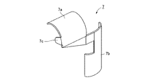
図1〜図4において、1はアノードキャップ、1aは中空円筒部、1bは頂部、1cはカバー部、1dは凸部、2は電圧供給ユニット、3は導電線、4はケーブル、5は接続部材、5aは嵌合部、6は電圧源、7は抜け防止材、7aはケーブル保持部、7bは接続部材保持部、11は表示パネルの基板、12は固定部材、12aは凹部、12bは貫通孔、13は封止部材、14、15は接着材、16はアノード端子、21は基板、22は外枠、23は弾性部材、24は引き出し配線、25はメタルバック、26は蛍光膜、27は電子源である。
1-4, 1 is an anode cap, 1a is a hollow cylindrical part, 1b is a top part, 1c is a cover part, 1d is a convex part, 2 is a voltage supply unit, 3 is a conductive wire, 4 is a cable, 5 is a connection Members, 5a is a fitting portion, 6 is a voltage source, 7 is a slip prevention member, 7a is a cable holding portion, 7b is a connection member holding portion, 11 is a display panel substrate, 12 is a fixing member, 12a is a recess, and 12b is Through hole, 13 is a sealing member, 14 and 15 are adhesives, 16 is an anode terminal, 21 is a substrate, 22 is an outer frame, 23 is an elastic member, 24 is a lead-out wiring, 25 is a metal back, 26 is a fluorescent film,
本発明のアノードキャップ1は絶縁性部材からなり、アノード端子16に電圧を供給する導電線3の一端を保持する保持部と、アノード端子16の周囲に固定された部材である固定部材12に係止する係止部とを有している。図1,2の実施形態においては、保持部として中空円筒部1aと、係止部として後述するように固定部材12を内側に嵌め込む空間が形成されている。
The anode cap 1 of the present invention is made of an insulating member, and is related to a holding portion that holds one end of a conductive wire 3 that supplies a voltage to the
図1のアノードキャップ1の内側には、固定部材12の外周に形成された凹部12aに対応する位置に凸部1dを有しており、アノードキャップ1が該固定部材12を覆った際に、図4に示すように、凸部1dが凹部12a内に入り込んでアノードキャップ1を固定部材12に固定することができる。本発明において、アノードキャップ1と固定部材12との係止形態は特に限定されず、取り付け後に多少の衝撃でも脱離せず、且つ、取り外しが容易であればどのような形態でも適用可能であるが、図1〜図4に示すように、アノードキャップ1の内側と固定部材12の外周にそれぞれ、対応する凸部または凹部を形成しておくことにより、該アノードキャップ1を容易に着脱可能とすることができる。凸部及び凹部の形状については特に限定されないが、着脱を容易にする上で弾性を有することが好ましく、よって、少なくともかかる凸部または凹部を含む部位を弾性素材で構成することが好ましく、具体的にはシリコーンゴムが好ましく用いられる。また、固定部材12とアノードキャップ1とを一方を他方にネジ式に嵌め込むことで係止する形態も好ましく適用される。
The anode cap 1 in FIG. 1 has a
さらに、本発明のアノードキャップ1は、中空円筒部1aや頂部1b、カバー部1cにおいても適度な弾性を有することが好ましく、凸部1dを含めて全体を一体で弾性素材で形成することが好ましい。具体的にはシリコーンゴムを用いて射出成形により形成するのが好ましい。
Further, the anode cap 1 of the present invention preferably has appropriate elasticity also in the hollow cylindrical portion 1a, the
本発明の電圧供給ユニット2はアノードキャップ1と該アノードキャップ1の保持部に一端を保持された導電線3とを有する。図2の実施形態においては、該導電線3の一端をアノードキャップ1内で固定してアノード端子16との良好な電気的接続を図るため、導電材からなる接続部材5を用いている。接続部材5は一端に設けた嵌合部に導電線3の先端を挿入して半田付け(不図示)により固定しており、該接続部材5の他端にはアノード端子16を挿入する嵌合部5aが形成されている。接続部材5としては、真鍮などが好ましく用いられる。
The voltage supply unit 2 of the present invention includes an anode cap 1 and a conductive wire 3 held at one end by a holding portion of the anode cap 1. In the embodiment of FIG. 2, the
また、接続部材5はアノードキャップ1の頂部1bで保持されているが、該頂部1bからの脱落を防止するために、ステンレスの板材などからなる抜け防止材7を用いることが好ましい。図2に示す7aはこの抜け防止材7のケーブル保持部、7bは接続部材保持部であり、全体を図5に、該抜け防止材にケーブル4と接続部材5を取り付けた様子を図6にそれぞれ示す。当該抜け防止材7にはケーブル保持部7aの端部にケーブル4側に先端が向いた爪7cが形成されており、該爪7cの先端をケーブル4に食い込ませることでケーブル保持部7aをケーブル4に機械的に固定し、接続部材保持部7bは接続部材5にかしめることで固定される。このような抜け防止材7を用いることで、導電線3と接続部材5との半田付け部位にかかるストレスが緩和される。
Further, the connecting
本発明の電圧供給ユニット2には、図2に示すように導電線3の他端に電圧源6が接続されるが、必要に応じてコネクタを介して接続することにより、導電線3を着脱可能とすることができる。電圧源6としては、従来のテレビジョン受像機の陰極線管で使用される、フライバックトランス等で昇圧した直流高電圧を発生するものが用いられる。 As shown in FIG. 2, the voltage source 6 is connected to the other end of the conductive wire 3 in the voltage supply unit 2 of the present invention. Can be possible. As the voltage source 6, one that generates a DC high voltage boosted by a flyback transformer or the like used in a cathode ray tube of a conventional television receiver is used.
本発明においては、このような電圧供給ユニット2を表示パネルのアノード端子16に対して着脱可能に取り付けるため、該ユニット2に何らかの不具合が生じた場合には、該ユニット2ごと交換することで繁雑な不具合部位の特定作業を回避することができる。
In the present invention, since such a voltage supply unit 2 is detachably attached to the
本発明の電圧供給ユニット2を取り付ける表示パネルのアノード端子周辺構造としては、図3に示すように、パネル外面に固定されたアノード端子16の周囲に固定部材12が固定されている。図3の構成においては、表示パネルの外面を構成する基板11にはアノード端子16と内部の引き出し配線24との導通を図るための開口部11aが形成され、該開口部11aが外側から封止部材13により塞がれている。封止部材13は接着材14により基板11に接着固定されており中央に設けられた貫通孔にアノード端子16が挿入されて固定されている。さらに、該アノード端子16の周囲を囲むように、中央に貫通孔12bを形成した固定部材12が接着材15により基板11に接着固定されている。
As the anode terminal peripheral structure of the display panel to which the voltage supply unit 2 of the present invention is attached, as shown in FIG. 3, a
本発明において、アノード端子16は、例えばAg、Cu、Ni−Co合金材等の導電材料からなり、封止部材13は、例えば、アルミナ等のセラミック、ガラスなどからなる円形板状部材が用いられ、中央にアノード端子16を保持する貫通孔が形成される。貫通孔に挿入したアノード端子16と封止部材13とは該貫通孔においてAg−Cu、Au−Niなどのろう材料にてろう付けすることにより気密封止される。
In the present invention, the
また、基板11の開口部11aは、例えば円形で、超音波加工機などを用いた機械加工によって形成される。封止部材13は該開口部11aを封止できるものであれば、円形に限らず、また、開口部11aの断面形状も円形に限られるものではない。
Moreover, the
図3のような固定部材12の貫通孔12b内に、図2の電圧供給ユニット2の接続部材5を差し込むことにより、接続部材5の嵌合部5aにアノード端子16が挿入されてアノード端子16が接続部材5を介して導電線3に電気的に接続され、同時に、上記したように、固定部材12がアノードキャップ1内に嵌め込まれ、凸部1dが凹部12a内に入り込むことでアノードキャップ1が固定部材12に固定され、図4に示すように電圧供給ユニット2が表示パネルに一体固定化される。
By inserting the connecting
本発明に用いられる固定部材12は、アノードキャップ1を容易に着脱しうるように、アノードキャップ1と同様に弾性素材で形成されていることが好ましく、例えば、PBT(ポリブチレンテレフタレート)樹脂などの弾性素材が好ましい。当該固定部材12はリンク状部材が好ましく用いられるが、本発明においては当該形状に限定されるものではなく、アノード端子16の周囲に不連続に配置された複数の部材から構成されるものであっても良く、取り付けられたアノードキャップが多少の衝撃にも脱離せず、且つ、容易に取り外しできる形状であれば適宜用いることができる。また、本実施形態においては、アノードキャップ1の内側に固定部材12が嵌め込まれる形態を示したが、本発明においてはアノードキャップ1と固定部材12とが着脱可能に係止されれば当該形態に限定されるものではない。
The
上記した封止部材13と基板11とは接着材14により接着固定されているが、該接着材14としては例えばフリットなどの低融点ガラスが用いられる。また、固定部材12と基板11とは接着材15により接着固定されているが、該接着材15としては例えばエポキシ系接着剤や硬化性シリコーンゴム等が用いられる。
The sealing
本発明の電圧供給ユニット2を表示パネルに取り付けた際の、アノードキャップ1と基板11との間の密着性は、図4における凸部1dによる基板11方向へのアノードキャップ1の押しつけ力と、アノードキャップ1のカバー部1cの湾曲した端部による該押しつけ力に対する反発力とによって得られるが、好ましくは、カバー部1cと基板11との間に絶縁グリースを介在させることで、その密着性を向上させることができる。
The adhesion between the anode cap 1 and the
図2の電圧供給ユニット2の図3の表示パネルへの装着は次のようにして行われる。 The voltage supply unit 2 of FIG. 2 is attached to the display panel of FIG. 3 as follows.
先ず、アノードキャップ1の椀状のカバー部1cの端部を、接続部材5の側面が半分以上見える程度まで捲り上げる。次に、固定部材12の中央に位置しているアノード端子16を接続部材5の嵌合部5aに挿入しながら接続部材5を固定部材12の貫通孔12a内に挿入して嵌合する。その後、捲り上げたカバー部1cを元に戻しながら内側の凸部1dを固定部材12の凹部12内に入れ込み、係止させる。
First, the end portion of the bowl-shaped
また、図4のように表示パネルに装着された電圧供給ユニット2の取り外しは次のようにして行う。 Further, the voltage supply unit 2 attached to the display panel as shown in FIG. 4 is removed as follows.
先ず、アノードキャップ1の椀状のカバー部1cの端部を捲り上げながら、内側の凸部1dを凹部12から引き出す。次に、カバー部1cの端部を、固定部材12の貫通孔12aから突出した接続部材5が見える位置まで捲り上げ、接続部材5を該貫通孔12aから引き抜くことで、電圧供給ユニット2を表示パネルから取り外す。
First, the inner
図4は、本発明の画像表示装置を平面型の表示パネルに適用した場合の構成例であり、電圧供給ユニット2を取り付けた基板11に対向する基板21側にアノード電位を供給する形態である。
FIG. 4 is a configuration example when the image display device of the present invention is applied to a flat display panel, and an anode potential is supplied to the
図4の実施形態では、電子源27が配置された基板(リアプレート)11と蛍光膜26及びメタルバック(アノード電極)25が設けられた基板(フェースプレート)21とが対向して配置されており、さらに基板11と21との間には外枠22が配置されて、これら基板11、21、外枠22で気密容器が構成されている。図7に該気密容器の分解模式図を示す。当該気密容器は内部が減圧雰囲気、好ましくは10-4〜10-6Paに保持される。外枠22は枠状に加工された部材と、該枠状の部材を基板11,21に接着するためのガラスまたは金属などからなる封着材とで構成される。基板11,21,枠状部材には青板ガラスや表面にSiO2被膜を形成した青板ガラス、Na含有量を低減したガラス、石英ガラスなどの各種材料を用いることができる。
In the embodiment of FIG. 4, a substrate (rear plate) 11 on which an
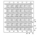
図8は電子源27の構成例の平面模式図であり、図中、82,83は素子電極、84は導電性膜、85は導電性膜84に形成された電子放出部、86は列方向配線、87は層間絶縁層、88は行方向配線であり、素子電極82,83と、電子放出部85を有する導電性膜84からなる表面伝導型の電子放出素子を、層間絶縁層87を介して配置された複数の列方向配線86と行方向配線88でマトリクス配線した形態である。本発明にかかる電子源27には、電界放出型素子(FE:フィールドエミッター)や表面伝導型電子放出素子、或いはMIM型素子が好ましく用いられる。
FIG. 8 is a schematic plan view of a configuration example of the
また、図9に蛍光膜26の平面構成例を示す。図中、91は蛍光体、92は黒色導電体であり、図9に示すように、R(赤)、G(緑)、B(青)の蛍光体91と、隣接する蛍光体91間を遮光する黒色導電体92から構成される。尚、図9においてはライン状の黒色導電体92がX方向、Y方向に複数本交差したブラックマトリクスの例を示したが、ライン状の黒色導電体が一方向に平行に複数本配置するブラックストライプを用いてもよい。
FIG. 9 shows an example of a planar configuration of the
蛍光膜26の内面側にはアノード電極を兼ねたメタルバック25が形成され、電子源27から放出された電子を加速させると同時に、蛍光膜26から基板11方向への発光を基板21側に反射する。
A metal back 25 also serving as an anode electrode is formed on the inner surface side of the
図8の列方向配線86、行方向配線88は不図示の引き出し配線に接続され、該引き出し配線が基板11と外枠22との間の絶縁性の封着材に埋設されて気密容器の外に引き出され、電子源27の駆動のための外部電源と接続される。
The
また、図4のメタルバック25は基板21の隅(コーナー部)に向かって引き出された引き出し配線24に接続され、この引き出し配線24と基板11に取り付けられたアノード端子16とが導電性の弾性部材23によって電気的に接続され、該アノード端子16が接続された電圧供給ユニット2を介して電圧源6よりアノード電位が供給される。
4 is connected to a
引き出し配線24は、例えばAgなどの導電材料からなり、印刷法などにより形成される。弾性部材23はステンレス等の導電材料からなるバネ部材であり、引き出し配線24を押圧してアノード端子16と引き出し配線24との電気的接続をより一層確実にすることができる。弾性部材23とアノード端子16との接続は、レーザ溶接、導電性接着剤、金属接合等の方法が用いられる。尚、本発明においては、弾性部材23を用いずに、アノード端子16を直接引き出し配線24に接続してもかまわない。
The
上記構成により、電子源27には、例えば、10〜100Vの低電位が供給され、一方、メタルバック25には、例えば、500V〜30kVの高電位が供給されることで、電子源27から放出された電子が加速して蛍光体92に照射し、画像の表示がなされる。
With the above configuration, the
1 アノードキャップ
1a 中空円筒部
1b 頂部
1c カバー部
1d 凸部
2 電圧供給ユニット
3 導電線
4 ケーブル
5 接続部材
5a 端子嵌合部
6 電圧源
7 抜け防止材
7a ケーブル保持部
7b 接続部材保持部
7c 爪
11 基板
11a 開口部
12 固定部材
12a 凹部
12b 貫通孔
13 封止部材
14、15 接着材
16 アノード端子
21 基板
22 外枠
23 弾性部材
24 引き出し配線
25 メタルバック
26 蛍光膜
27 電子源
82,83 素子電極
84 導電性膜
85 電子放出部
86 列方向配線
87 層間絶縁層
88 行方向配線
91 蛍光体
92 黒色導電体
DESCRIPTION OF SYMBOLS 1 Anode cap 1a Hollow
Claims (4)
前記アノード電極は前記表示パネルの内部に設けられており、
前記アノード端子は前記アノード電極に前記表示パネルの外側から電圧を供給するための端子であって、前記表示パネルの内部に位置する部分と前記表示パネルの外部に位置する部分とを備えており、
前記部材は、前記アノード端子の、前記表示パネルの外部に位置する部分が挿入された貫通孔を備えており、且つ、前記表示パネルの外表面に固定されており、
前記アノードキャップは、弾性素材で構成された椀状のカバー部を有し、該カバー部の端部が前記部材の周囲の前記表示パネル外表面に弾性的に押し付けられた状態で前記部材によって係止される係止部を前記カバー部の内側に有することを特徴とする画像表示装置。 An image display comprising: a display panel including at least an anode electrode and an anode terminal; an anode cap for holding a conductive wire for supplying a voltage to the anode terminal; and a member for detachably locking the anode cap. A device,
The anode electrode is provided inside the display panel,
The anode terminal is a terminal for supplying a voltage to the anode electrode from the outside of the display panel, and includes a portion located inside the display panel and a portion located outside the display panel,
The member includes a through-hole into which a portion of the anode terminal located outside the display panel is inserted, and is fixed to the outer surface of the display panel,
The anode cap has a bowl-shaped cover portion made of an elastic material, and the end portion of the cover portion is engaged with the member in a state of being elastically pressed against the outer surface of the display panel around the member. An image display device comprising a locking portion to be stopped inside the cover portion .
Priority Applications (4)
| Application Number | Priority Date | Filing Date | Title |
|---|---|---|---|
| JP2005110707A JP4557781B2 (en) | 2005-04-07 | 2005-04-07 | Image display device |
| US11/376,239 US7619354B2 (en) | 2005-04-07 | 2006-03-16 | Anode cap, and voltage supply unit and image display apparatus utilizing the same |
| CNB2006100733065A CN100530505C (en) | 2005-04-07 | 2006-04-07 | Anode cap, and voltage supply unit and image display apparatus utilizing the same |
| US12/561,307 US8093794B2 (en) | 2005-04-07 | 2009-09-17 | Anode cap, and voltage supply unit and image display apparatus utilizing the same |
Applications Claiming Priority (1)
| Application Number | Priority Date | Filing Date | Title |
|---|---|---|---|
| JP2005110707A JP4557781B2 (en) | 2005-04-07 | 2005-04-07 | Image display device |
Publications (3)
| Publication Number | Publication Date |
|---|---|
| JP2006294324A JP2006294324A (en) | 2006-10-26 |
| JP2006294324A5 JP2006294324A5 (en) | 2010-06-03 |
| JP4557781B2 true JP4557781B2 (en) | 2010-10-06 |
Family
ID=37064217
Family Applications (1)
| Application Number | Title | Priority Date | Filing Date |
|---|---|---|---|
| JP2005110707A Expired - Fee Related JP4557781B2 (en) | 2005-04-07 | 2005-04-07 | Image display device |
Country Status (3)
| Country | Link |
|---|---|
| US (2) | US7619354B2 (en) |
| JP (1) | JP4557781B2 (en) |
| CN (1) | CN100530505C (en) |
Families Citing this family (6)
| Publication number | Priority date | Publication date | Assignee | Title |
|---|---|---|---|---|
| JP2009037792A (en) * | 2007-07-31 | 2009-02-19 | Hitachi Displays Ltd | Image display device |
| JP2009145822A (en) * | 2007-12-18 | 2009-07-02 | Canon Inc | Image display apparatus |
| JP2010218754A (en) * | 2009-03-13 | 2010-09-30 | Canon Inc | Image displaying apparatus |
| JP2012003060A (en) | 2010-06-17 | 2012-01-05 | Canon Inc | Image display device, holding member thereof, and image display system |
| JP2014082089A (en) * | 2012-10-16 | 2014-05-08 | Sumitomo Wiring Syst Ltd | Rubber boot |
| CN107453079B (en) * | 2017-07-18 | 2019-08-30 | 番禺得意精密电子工业有限公司 | Electric connector |
Citations (2)
| Publication number | Priority date | Publication date | Assignee | Title |
|---|---|---|---|---|
| JPH0292648U (en) * | 1989-01-10 | 1990-07-23 | ||
| JP2000251981A (en) * | 1999-02-24 | 2000-09-14 | Canon Inc | Anode cap and flat-panel image display device using same |
Family Cites Families (8)
| Publication number | Priority date | Publication date | Assignee | Title |
|---|---|---|---|---|
| US4894023A (en) * | 1988-09-06 | 1990-01-16 | Hall Harold E | Connector assembly for anode ring of cathode ray tube |
| JPH0292648A (en) | 1988-09-30 | 1990-04-03 | Toshiba Corp | Head driving device for electroconduction transfer printer |
| JPH0729626A (en) | 1993-07-12 | 1995-01-31 | Taisho Denki Kogyo Kk | Anode cap |
| CN1380678A (en) * | 2001-04-10 | 2002-11-20 | 珀斯泰克有限公司 | Anode cap and its manufacturing device and method |
| US7102701B2 (en) * | 2001-12-27 | 2006-09-05 | Canon Kabushiki Kaisha | Display device |
| JP3984942B2 (en) * | 2002-09-26 | 2007-10-03 | キヤノン株式会社 | Image display device and information display device |
| JP3940841B2 (en) * | 2002-12-27 | 2007-07-04 | キヤノン株式会社 | Display device |
| JP4103679B2 (en) * | 2003-05-21 | 2008-06-18 | 株式会社日立製作所 | Display device |
-
2005
- 2005-04-07 JP JP2005110707A patent/JP4557781B2/en not_active Expired - Fee Related
-
2006
- 2006-03-16 US US11/376,239 patent/US7619354B2/en not_active Expired - Fee Related
- 2006-04-07 CN CNB2006100733065A patent/CN100530505C/en not_active Expired - Fee Related
-
2009
- 2009-09-17 US US12/561,307 patent/US8093794B2/en not_active Expired - Fee Related
Patent Citations (2)
| Publication number | Priority date | Publication date | Assignee | Title |
|---|---|---|---|---|
| JPH0292648U (en) * | 1989-01-10 | 1990-07-23 | ||
| JP2000251981A (en) * | 1999-02-24 | 2000-09-14 | Canon Inc | Anode cap and flat-panel image display device using same |
Also Published As
| Publication number | Publication date |
|---|---|
| US20060228951A1 (en) | 2006-10-12 |
| CN100530505C (en) | 2009-08-19 |
| US8093794B2 (en) | 2012-01-10 |
| JP2006294324A (en) | 2006-10-26 |
| US20100007265A1 (en) | 2010-01-14 |
| CN1845290A (en) | 2006-10-11 |
| US7619354B2 (en) | 2009-11-17 |
Similar Documents
| Publication | Publication Date | Title |
|---|---|---|
| KR100796089B1 (en) | Display device | |
| JP4557781B2 (en) | Image display device | |
| EP0866490A2 (en) | Image-forming apparatus | |
| KR100516606B1 (en) | Display device, hermetic container, and method for manufacturing hermetic container | |
| JP2003092075A (en) | Electron beam device and image display device | |
| KR20040095010A (en) | Field emission display device | |
| JP2006252979A (en) | Image display device | |
| JP4250608B2 (en) | Image display device and manufacturing method thereof | |
| JP4103679B2 (en) | Display device | |
| US20070069630A1 (en) | Image display device | |
| JP2006202553A (en) | Image display device and its manufacturing method | |
| KR20070083124A (en) | Electron emission display device | |
| JP4865235B2 (en) | Image display device | |
| JP2006222093A (en) | Electron beam device and image display device | |
| JP2007073467A (en) | Image display | |
| JP2008004323A (en) | Image display device | |
| WO2006006365A1 (en) | Display device | |
| US20100231115A1 (en) | Image displaying apparatus | |
| JPH04308636A (en) | Thin cathode-ray tube | |
| JPS6226750A (en) | Fixing structure of fluorescent character display tube | |
| JP2007280859A (en) | Image display device | |
| JP2008251365A (en) | Image display device | |
| JP2004014254A (en) | Cathode support fixing structure for fluorescent display tube | |
| JP2003198987A (en) | Display | |
| JP2007227313A (en) | Image display device |
Legal Events
| Date | Code | Title | Description |
|---|---|---|---|
| A621 | Written request for application examination |
Free format text: JAPANESE INTERMEDIATE CODE: A621 Effective date: 20080327 |
|
| A711 | Notification of change in applicant |
Free format text: JAPANESE INTERMEDIATE CODE: A711 Effective date: 20080619 |
|
| A521 | Written amendment |
Free format text: JAPANESE INTERMEDIATE CODE: A523 Effective date: 20100415 |
|
| A977 | Report on retrieval |
Free format text: JAPANESE INTERMEDIATE CODE: A971007 Effective date: 20100423 |
|
| A131 | Notification of reasons for refusal |
Free format text: JAPANESE INTERMEDIATE CODE: A131 Effective date: 20100427 |
|
| A521 | Written amendment |
Free format text: JAPANESE INTERMEDIATE CODE: A523 Effective date: 20100617 |
|
| TRDD | Decision of grant or rejection written | ||
| A01 | Written decision to grant a patent or to grant a registration (utility model) |
Free format text: JAPANESE INTERMEDIATE CODE: A01 Effective date: 20100713 |
|
| A01 | Written decision to grant a patent or to grant a registration (utility model) |
Free format text: JAPANESE INTERMEDIATE CODE: A01 |
|
| A61 | First payment of annual fees (during grant procedure) |
Free format text: JAPANESE INTERMEDIATE CODE: A61 Effective date: 20100720 |
|
| R150 | Certificate of patent or registration of utility model |
Free format text: JAPANESE INTERMEDIATE CODE: R150 |
|
| FPAY | Renewal fee payment (event date is renewal date of database) |
Free format text: PAYMENT UNTIL: 20130730 Year of fee payment: 3 |
|
| LAPS | Cancellation because of no payment of annual fees |