JP2009087908A - Organic el element - Google Patents
Organic el element Download PDFInfo
- Publication number
- JP2009087908A JP2009087908A JP2007260003A JP2007260003A JP2009087908A JP 2009087908 A JP2009087908 A JP 2009087908A JP 2007260003 A JP2007260003 A JP 2007260003A JP 2007260003 A JP2007260003 A JP 2007260003A JP 2009087908 A JP2009087908 A JP 2009087908A
- Authority
- JP
- Japan
- Prior art keywords
- layer
- organic
- color
- color filter
- display
- Prior art date
- Legal status (The legal status is an assumption and is not a legal conclusion. Google has not performed a legal analysis and makes no representation as to the accuracy of the status listed.)
- Withdrawn
Links
Images


Abstract
Description
本発明は、有機EL素子に関する。詳細には、非点灯時の物体色が制御された有機EL素子に関する。 The present invention relates to an organic EL element. Specifically, the present invention relates to an organic EL element in which the object color when not lit is controlled.
現在、さまざまな分野・用途において種々の表示装置が用いられている。これらの表示装置は、その機構に基づいて自発光型と非発光型の2つのタイプに分類される。自発光型表示装置の代表例は、陰極管(CRT)、EL(エレクトロルミネセンス)ディスプレイ、FED(フィールド・エミッション・ディスプレイ)などを含む。一方、非発光型表示装置の代表例は、液晶表示装置である。 Currently, various display devices are used in various fields and applications. These display devices are classified into two types of self-luminous type and non-luminous type based on the mechanism. Typical examples of the self-luminous display device include a cathode ray tube (CRT), an EL (electroluminescence) display, an FED (field emission display), and the like. On the other hand, a typical example of a non-light-emitting display device is a liquid crystal display device.
これらのディスプレイでは、赤(R)、緑(G)、および青(B)の3原色を用いたマルチカラーまたはフルカラー方式がほぼ一般的となっている。より高品位で美しい画像を表示させるために、発光部と光出射面との間にカラーフィルター等の色変調層を配置して、発光素子を発した光のうちの特定の波長域の光を選択的に出射させて、3原色の色純度を向上させる手段が多用されている。 In these displays, a multi-color or full-color system using three primary colors of red (R), green (G), and blue (B) is almost common. In order to display a high-quality and beautiful image, a color modulation layer such as a color filter is disposed between the light emitting portion and the light emitting surface, and light in a specific wavelength region out of the light emitted from the light emitting element. Means for selectively emitting and improving the color purity of the three primary colors are frequently used.
近年では、色変調層として、有機EL素子の発光域の光を吸収し、可視光域の蛍光を発光する蛍光材料を色変換層として用いる色変換方式の有機ELディスプレイが開示されている(特許文献1など参照)。色変換方式のディスプレイにおいては、有機EL素子の発光色が白色に限定されないため、より輝度の高い有機EL素子を光源に適用できる。例えば、青色発光の有機EL素子を用いた場合には、青色光を緑色光および赤色光に波長変換する(特許文献1参照)。このような蛍光材料を含む色変換層を高精細にパターニングして、有機EL素子の近紫外光ないし可視光のような弱いエネルギー線を用いて3原色の光を得る色変換方式フルカラーディスプレイが注目されている。
In recent years, as a color modulation layer, a color conversion type organic EL display using a fluorescent material that absorbs light in an emission region of an organic EL element and emits fluorescence in a visible light region as a color conversion layer has been disclosed (patent)
この色変換方式有機ELディスプレイに用いられる色変換層は、フォトレジストを用いるウェットプロセスによって形成することができる。しかしながら、色変換材料の耐熱性が低いために、ウェットプロセスで用いた色変換材料を含むフォトレジストを完全に乾燥させることは困難である。そのため、乾燥後に色変換層中に残存する水分により、有機EL素子中にダークエリアとも呼ばれる非発光欠陥を発生させるという問題点が存在する。この問題点を解消するために、近年、ウェットプロセスに代えてドライプロセスを用いて色変換層を形成することが検討されている(特許文献2参照)。 The color conversion layer used in this color conversion organic EL display can be formed by a wet process using a photoresist. However, since the color conversion material has low heat resistance, it is difficult to completely dry the photoresist including the color conversion material used in the wet process. Therefore, there is a problem that non-light-emitting defects, also called dark areas, are generated in the organic EL element due to moisture remaining in the color conversion layer after drying. In order to solve this problem, it has recently been studied to form a color conversion layer using a dry process instead of a wet process (see Patent Document 2).
また、表示装置が使用される特定の分野・用途においては、非点灯時の表示装置の色を該装置を取り巻くボディーフレームの色と一致またはそれに釣り合った物体色(色調)にすること、および製品として使用される環境やその用途に応じて非点灯時の表示装置の物体色を自由に設計可能にすることが求められてきている。
この要求に対して、表示装置表面にフィルムを適用する方法が提案されてきている(特許文献3参照)。
Further, in a specific field / application in which the display device is used, the color of the display device when not lit is matched with the color of the body frame surrounding the device or an object color (color tone) that matches the color, and the product Therefore, it has been demanded that the object color of the display device when it is not lit can be designed freely according to the environment used and the application.
In response to this requirement, a method of applying a film to the surface of a display device has been proposed (see Patent Document 3).
色変換方式の表示装置における現時点での問題点の1つは、非点灯時の表示装置に外光が入射した場合に、表示装置の表示面が種々の色に色づいてしまうことである。これは、表示装置中の色変換層が形成された副画素の透過率と色変換層が形成されていない副画素の透過率が異なることにより、偏った波長分布を有する反射光が放射されるために起こる現象である。ドライプロセスによって色変換層を形成する表示装置においては、色変換層は、R、G、B副画素に応じて、色変換層が選択的に平坦化層の上に形成される。この場合、色変換層を形成しない部分からの光出射を増大させるために、平坦化層の透過率をより大きくすることが好ましい。より大きな透過率の平坦化層を用いるために、色変換層が形成された副画素の透過率と色変換層が形成されていない副画素の透過率との差は、さらに大きくなってしまう。 One of the problems at the present time in color conversion type display devices is that the display surface of the display device is colored in various colors when external light is incident on the non-lighted display device. This is because reflected light having a biased wavelength distribution is emitted because the transmittance of the sub-pixel in which the color conversion layer in the display device is formed is different from the transmittance of the sub-pixel in which the color conversion layer is not formed. This is a phenomenon that occurs. In the display device in which the color conversion layer is formed by a dry process, the color conversion layer is selectively formed on the planarization layer according to the R, G, and B subpixels. In this case, in order to increase light emission from a portion where the color conversion layer is not formed, it is preferable to increase the transmittance of the planarization layer. Since a flattening layer having a larger transmittance is used, the difference between the transmittance of the sub-pixel having the color conversion layer and the transmittance of the sub-pixel having no color conversion layer is further increased.
従来から提案されている表示装置表面に対する塗料またはフィルムの適用は、表示装置表面を着色させることに基づいて、非点灯時の表示装置の物体色(色調)を調整するものである。したがって、点灯時に色変換フィルタから放射される光もまた塗料ないしフィルムの影響を受け、所望されない色相を有する光が放射されてしまうこと、あるいはカラーフィルタ層において高められた色純度の低下などの問題を引き起こす恐れがある。 Conventionally proposed application of a paint or film to the surface of a display device adjusts the object color (color tone) of the display device when not lit based on coloring the surface of the display device. Therefore, the light emitted from the color conversion filter at the time of lighting is also affected by the paint or film, and the light having an undesired hue is emitted or the color purity is increased in the color filter layer. There is a risk of causing.
あるいはまた、ウェットプロセスによって形成される色変換層を用いる色変換方式有機ELディスプレイにおいて、色変換層、または色変換層が形成されない副画素の平坦化層に相分離剤を添加して、RGBそれぞれの副画素の透過率を変化させ、外光が入射した際の非点灯のディスプレイの物体色を調整することが提案されている(特許文献4参照)。しかしながら、ドライプロセスによって色変換層を形成する場合、蒸着される色変換層に対して相分離剤を添加して相分離を行うことが難しく、かつ形成される色変換層が薄いために、その効果も限定的であることが予想される。また、この方式のディスプレイにおいて、カラーフィルタ層を覆って一体に形成される平坦化層の一部のみに相分離剤を適用して、各副画素毎の透過率を変化させることは困難である。 Alternatively, in a color conversion type organic EL display using a color conversion layer formed by a wet process, a phase separation agent is added to the color conversion layer or a flattening layer of a sub-pixel where the color conversion layer is not formed, and each of RGB It has been proposed to adjust the object color of a non-lighted display when external light is incident by changing the transmittance of the sub-pixel (see Patent Document 4). However, when the color conversion layer is formed by a dry process, it is difficult to add a phase separation agent to the deposited color conversion layer and perform phase separation, and the formed color conversion layer is thin. The effect is also expected to be limited. In addition, in this type of display, it is difficult to change the transmittance for each sub-pixel by applying the phase separation agent to only a part of the flattening layer formed integrally to cover the color filter layer. .
したがって、ドライプロセスによって色変換層を形成する色変換方式有機ELディスプレイにおいて、表示装置表面を着色させることなしに、外光が入射した際の非点灯の表示装置の物体色(すなわち、反射光の色相)を制御することができる方法が、当該技術において強く求められている。 Therefore, in a color conversion type organic EL display in which a color conversion layer is formed by a dry process, the object color of a non-lighted display device (that is, reflected light) when external light is incident without coloring the display device surface. There is a strong need in the art for methods that can control hue.
上述の課題を解決するための方策について鋭意検討した結果、複数種のカラーフィルタ層において、1つ又は複数のカラーフィルタ層に相分離剤を添加して散乱光の量を独立的に変化させ、ディスプレイの物体色を調整する方法を見いだした。 As a result of earnestly examining the measures for solving the above-mentioned problems, in a plurality of types of color filter layers, the amount of scattered light is independently changed by adding a phase separation agent to one or a plurality of color filter layers, I found a way to adjust the object color of the display.
本発明の1つの態様である有機ELディスプレイは、透明基板と、2種以上のカラーフィルタ層と、少なくとも1種の色変換層と、透明電極、有機EL層および反射電極を含み、前記2種以上のカラーフィルタ層は、それぞれ独立的に制御された光の散乱量を有することを特徴とする。ここで、前記2種以上のカラーフィルタ層の散乱量の独立的な制御が、相分離剤の添加によって、カラーフィルタ層中に異なる屈折率を有する部分を生じさせることにより実施されてもよい。 An organic EL display according to one aspect of the present invention includes a transparent substrate, two or more color filter layers, at least one color conversion layer, a transparent electrode, an organic EL layer, and a reflective electrode. Each of the above color filter layers has a light scattering amount controlled independently of each other. Here, the independent control of the scattering amount of the two or more color filter layers may be performed by generating a portion having a different refractive index in the color filter layer by the addition of a phase separation agent.
本発明の1つの態様である有機ELディスプレイの物体色の調整方法は、透明基板と、2種以上のカラーフィルタ層と、少なくとも1種の色変換層と、透明電極、有機EL層および反射電極を含む有機EL素子とを含む有機ELディスプレイにおいて、前記カラーフィルタ層の少なくとも1つの光の散乱量を独立的に変化させる工程を含むことを特徴とする。前記カラーフィルタ層の少なくとも1つの光の散乱量を独立的に変化させる工程が、当該カラーフィルタ層に相分離剤を添加されることによって実施されてもよい。 The method for adjusting the object color of an organic EL display according to one aspect of the present invention includes a transparent substrate, two or more color filter layers, at least one color conversion layer, a transparent electrode, an organic EL layer, and a reflective electrode. An organic EL display including an organic EL element including: a step of independently changing a scattering amount of at least one light of the color filter layer. The step of independently changing at least one light scattering amount of the color filter layer may be performed by adding a phase separation agent to the color filter layer.
本発明により、有機ELディスプレイのカラーフィルタ層において、カラーフィルターに入射する外光の散乱量をそれぞれ独立に変化させることによって、有機ELディスプレイの性能(輝度および色度)を維持したまま、非点灯時に外光が入射したディスプレイの物体色を変化させることができた。 According to the present invention, in the color filter layer of the organic EL display, the amount of outside light incident on the color filter is independently changed, so that the performance (brightness and chromaticity) of the organic EL display is maintained and the light is not turned on. It was possible to change the object color of the display that was sometimes exposed to external light.
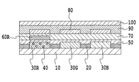
以下、本発明について詳細に説明する。図1〜図3は、本発明の有機ELディスプレイ(1画素分)を示す模式的断面図であり、図1は青色カラーフィルタ層に相分離剤を添加した例(実施例1)を示し、図2は緑色カラーフィルタ層に相分離剤を添加した例(実施例2)を示し、図3は赤色カラーフィルタ層に相分離剤を添加した例(実施例3)を示す。 Hereinafter, the present invention will be described in detail. 1 to 3 are schematic cross-sectional views showing an organic EL display (for one pixel) of the present invention. FIG. 1 shows an example (Example 1) in which a phase separator is added to a blue color filter layer. FIG. 2 shows an example (Example 2) in which a phase separator is added to the green color filter layer, and FIG. 3 shows an example (Example 3) in which a phase separator is added to the red color filter layer.
透明基板10は、可視光(波長400〜700nm)に対して透明であり、積層される層の形成に用いられる条件(溶媒、温度等)に耐えるものであるべきであり、および寸法安定性に優れていることが好ましい。好ましい透明基板は、ガラス基板、およびポリオレフィン、アクリル樹脂(ポリメチルメタクリレートを含む)、ポリエステル樹脂(ポリエチレンテレフタレートを含む)、ポリカーボネート樹脂、またはポリイミド樹脂などの樹脂で形成された剛直性の樹脂基板を含む。あるいはまた、ポリオレフィン、アクリル樹脂(ポリメチルメタクリレートを含む)、ポリエステル樹脂(ポリエチレンテレフタレートを含む)、ポリカーボネート樹脂、またはポリイミド樹脂などから形成される可撓性フィルムを、基板として用いてもよい。ガラス、ならびにポリエチレンテレフタレート、ポリメチルメタクリレート等の樹脂を含む。ホウケイ酸ガラスまたは青板ガラス等が特に好ましいものである。
The
遮光層20は、任意選択的に設けてもよい層であり、可視光を遮断して、コントラストを向上させるための層である。遮光層20は、通常のフラットパネルディスプレイ用の材料を用いて形成することができる。遮光層20は、1つの方向に延びるストライプ形状を有する複数の部分から構成されてもよいし、複数の開口部が2次元的に整列された一体の部分から構成されてもよい。
The
2種以上のカラーフィルタ層30は、入射光の特定の波長成分のみを透過させて、出力光の色純度を向上させるための層である。カラーフィルタ層30のそれぞれは、1つの方向に延びるストライプ形状を有する複数の部分から構成されてもよいし、副画素に相当する位置に形成される複数の独立した部分から構成されてもよい。図1〜図3においては、RGB3種のカラーフィルタ層30(R,G,B)を用いた例を示した。通常のフルカラーディスプレイの場合、赤色カラーフィルタ層30Rは600nm以上の波長成分を透過させ、緑色カラーフィルタ層30Rは500〜600nmの波長成分を透過させ、青色カラーフィルタ層30Bは400〜500nmの波長成分を透過させるように設計される。カラーフィルタ層30は、感光性樹脂中に色素を分散させた着色感材を塗布し、パターン状露光および現像を行うことによって、所望のパターンに形成されることが一般的である。最近では、耐久性の観点から、色素として顔料を使用することが多くなってきている。カラーフィルタ層2に用いることができる顔料は、アゾレーキ系、不溶性アゾ系、縮合アゾ系、フタロシアニン系、キナクリドン系、ジオキサジン系、イソインドリノン系、アントラキノン系、ペリノン系、チオイン系、ペリレン系、およびそれらの混合物などを含む。現在市販されているフラットパネルディスプレイ用のカラーフィルタ材料を用いてカラーフィルタ層2を形成してもよい。
The two or more color filter layers 30 are layers for transmitting only a specific wavelength component of incident light and improving the color purity of the output light. Each of the color filter layers 30 may be composed of a plurality of portions having a stripe shape extending in one direction, or may be composed of a plurality of independent portions formed at positions corresponding to sub-pixels. 1-3, the example using the RGB 3 types of color filter layer 30 (R, G, B) was shown. In the case of a normal full color display, the red
本発明においては、少なくとも1つのカラーフィルタ層30において、相分離剤40の添加によって層中にミクロ相分離を発生させ、他のカラーフィルタ層30とは独立して、光の散乱量を変化させる。図1は青色カラーフィルタ層30Bに相分離剤40を添加した例を示し、図2は緑色カラーフィルタ層30Gに相分離剤40を添加した例を示し、図3は赤色カラーフィルタ層30Rに相分離剤40を添加した例を示す。
In the present invention, in at least one color filter layer 30, microphase separation occurs in the layer by adding the
本発明において用いられる相分離剤40は、低分子化合物または高分子化合物であってもよく、好ましくはヒンダードアミン系化合物(例えばチバガイギー製チヌビン123など)、またはベンゾエート系ないしNi系の光安定剤として知られる化合物であってもよい。相分離剤40の添加によりカラーフィルタ層30中に相分離を発生させ、2つ以上のミクロに分離された相とすることにより、カラーフィルタ層30における散乱を増大させることができる。本発明に用いられる添加剤は、カラーフィルタ層30の総質量を基準として、0.01〜10.00質量%、より好ましくは0.10〜5.00質量%の量で用いられる。このような含有量で相分離剤40を用いることによって、非点灯時に入射する外光を充分に散乱させることが可能となる。
The
相分離剤40を含むカラーフィルタ層30は、前述の市販のカラーフィルタ層材料と相分離剤40との混合物を調製し、当該技術において知られている方法を用いて該混合物の塗布およびパターニングを実施することによって作製することができる。
The color filter layer 30 including the
平坦化層50は、遮光層20および2種以上のカラーフィルタ層30を覆うように形成される。平坦化層50は、任意選択的に設けてもよい層であるが、以下の目的のために設けることが好ましい層である。後述するように、色変換フィルタ上に透明電極80、有機EL層90および反射電極100を積層して有機EL素子を形成する場合に、平坦化層50は、透明電極80と反射電極100間の短絡の原因となる凹凸を平滑化するために有用である。平坦化層50は、その下に形成されるカラーフィルタ層30およびその上に形成される色変換層60の機能を損なうことなく形成することができ、かつ適度な弾力性を有する材料から形成することができる。平坦化層50は、単層から構成されてもよいし、複数の材料を積層したものであってもよい。
The
平坦化層50は、光透過性に富み、その下に形成されるカラーフィルタ層30およびその上に形成される色変換層80を劣化させることなしに形成することができ、かつ適度な弾力性を有する材料から形成される。たとえば、光硬化性または光熱併用型硬化性樹脂を塗布し、続いて光および/または熱処理して、ラジカル種やイオン種を発生させて重合または架橋させ、不溶不融化させることによって、平坦化層50を形成することができる。用いることができる光硬化性または光熱併用型硬化性樹脂は、(1)アクロイル基やメタクロイル基を複数有するアクリル系多官能モノマーおよびオリゴマーと、光または熱重合開始剤とからなる組成物、(2)ポリビニル桂皮酸エステルと増感剤とからなる組成物、(3)鎖状または環状オレフィンとビスアジドとからなる組成物、または(4)エポキシ基を有するモノマーと光酸発生剤からなる組成物を含む。特に、高精細でパターニングが可能であり、ならびに耐溶剤性および耐熱性などの信頼性のが高いことにより、(1)の組成物が好ましい。なお、部分的に光および/または熱処理して平坦化層50のパターニングを実施する場合には、未硬化の状態で有機溶媒またはアルカリ溶媒に可溶性の樹脂を用いることが好ましい。
The
あるいはまた、ポリカーボネート(PC)、ポリエチレンテレフタレート(PET)、ポリエーテルサルホン、ポリビニルブチラール、ポリフェニレンエーテル、ポリアミド、ポリエーテルイミド、ノルボルネン系樹脂、メタクリル樹脂、イソブチレン無水マレイン酸共重合樹脂、環状オレフィン系などの熱可塑性樹脂;エポキシ樹脂、フェノール樹脂、ウレタン樹脂、アクリル樹脂、ビニルエステル樹脂、イミド系樹脂、ウレタン系樹脂、ユリア樹脂、メラミン樹脂などの熱硬化性樹脂;あるいはポリスチレン、ポリアクリロニトリル、ポリカーボネート等と3官能性、あるいは4官能性のアルコキシシランを含むポリマーハイブリッド等を用いて、平坦化層50を形成してもよい。この場合には、これら材料の溶液または分散液を塗布した後に、溶媒または分散媒の除去、ならびに、必要に応じて硬化処理を行うことによって平坦化層を得ることができる。
Alternatively, polycarbonate (PC), polyethylene terephthalate (PET), polyethersulfone, polyvinyl butyral, polyphenylene ether, polyamide, polyetherimide, norbornene resin, methacrylic resin, isobutylene maleic anhydride copolymer resin, cyclic olefin, etc. Thermosetting resins such as epoxy resins, phenol resins, urethane resins, acrylic resins, vinyl ester resins, imide resins, urethane resins, urea resins, melamine resins; or polystyrene, polyacrylonitrile, polycarbonate, etc. The
少なくとも1種の色変換層60は、ドライプロセス、好ましくは蒸着法(抵抗加熱および電子ビーム加熱を含む)によって形成される層である。本発明の色変換層60は、有機樹脂などの結合剤を含まず、1種または複数種の色変換色素からなる層である。色変換層60を構成する色変換色素は水分に弱く、画像欠陥であるダークエリアの発生を抑制するためにも、下地となるカラーフィルタ層30および平坦化層50の形成に際して、それらの層を高温で完全に乾燥させることが必要である。
The at least one color conversion layer 60 is a layer formed by a dry process, preferably an evaporation method (including resistance heating and electron beam heating). The color conversion layer 60 of the present invention is a layer that does not contain a binder such as an organic resin and is composed of one or more color conversion dyes. The color conversion dye constituting the color conversion layer 60 is weak against moisture, and in order to suppress the occurrence of dark areas that are image defects, these layers are used when forming the color filter layer 30 and the
色変換層60のそれぞれは、1つの方向に延びるストライプ形状を有する複数の部分から構成されてもよいし、副画素に相当する位置に形成される複数の独立した部分から構成されてもよい。図1〜図3においては、赤色副画素に赤色変換層60Rを配設した1種の色変換層60を用いる構成例を示した。しかしながら、必要に応じて、緑色副画素および青色副画素に緑色変換層60Gおよび青色変換層60Bを配設してもよい。 Each of the color conversion layers 60 may be composed of a plurality of portions having a stripe shape extending in one direction, or may be composed of a plurality of independent portions formed at positions corresponding to sub-pixels. FIGS. 1 to 3 show configuration examples using one type of color conversion layer 60 in which a red conversion layer 60 </ b> R is disposed in a red subpixel. However, if necessary, the green conversion layer 60G and the blue conversion layer 60B may be disposed on the green subpixel and the blue subpixel.
色変換層60は、好ましくは1μm以下、より好ましくは200nm〜1μmの膜厚を有する。複数種の色変換色素を用いて色変換層60を形成する場合、複数種の色変換色素を所定の比率で混合した予備混合物をあらかじめ作製し、その予備混合物を用いて共蒸着を行ってもよい。あるいはまた、複数種の色変換色素を別個の加熱部位に配置し、それぞれの色変換色素を別個に加熱して共蒸着を行ってもよい。特に複数種の色変換色素の間に特性(蒸着速度、蒸気圧など)の大きな差が存在する場合、後者の方法が有効である。 The color conversion layer 60 preferably has a thickness of 1 μm or less, more preferably 200 nm to 1 μm. When the color conversion layer 60 is formed using a plurality of types of color conversion dyes, a preliminary mixture obtained by mixing a plurality of types of color conversion dyes at a predetermined ratio may be prepared in advance, and co-evaporation may be performed using the preliminary mixture. Good. Alternatively, a plurality of types of color conversion dyes may be disposed in separate heating portions, and the respective color conversion dyes may be separately heated to perform co-evaporation. In particular, the latter method is effective when there is a large difference in characteristics (evaporation rate, vapor pressure, etc.) among a plurality of types of color conversion dyes.
色変換層60を形成するための色変換色素としては、3−(2−ベンゾチアゾリル)−7−ジエチルアミノクマリン(クマリン6)、3−(2−ベンゾイミダゾリル)−7−ジエチルアミノクマリン(クマリン7)、クマリン135などのクマリン系色素;ソルベントイエロー43、ソルベントイエロー44のようなナフタルイミド系色素;4−ジシアノメチレン−2−メチル−6−(p−ジメチルアミノスチリル)−4H−ピラン(DCM−1、(I))、DCM−2(II)、およびDCJTB(III)などのシアニン色素;ローダミンB、ローダミン6Gなどのキサンテン系色素;ピリジン1などのピリジン系色素;ジエチルキナクリドン(DEQ)などのキナクリドン誘導体;4,4−ジフルオロ−1,3,5,7−テトラフェニル−4−ボラ−3a,4a−ジアザ−s−インダセン(IV)、ルモゲンFレッド、ナイルレッド(V)などを用いることができる。
Examples of the color conversion dye for forming the color conversion layer 60 include 3- (2-benzothiazolyl) -7-diethylaminocoumarin (coumarin 6), 3- (2-benzimidazolyl) -7-diethylaminocoumarin (coumarin 7), and coumarin. Coumarin dyes such as 135; naphthalimide dyes such as Solvent Yellow 43 and Solvent Yellow 44; 4-dicyanomethylene-2-methyl-6- (p-dimethylaminostyryl) -4H-pyran (DCM-1, ( I)), cyanine dyes such as DCM-2 (II) and DCJTB (III); xanthene dyes such as rhodamine B and rhodamine 6G; pyridine dyes such as

複数種、たとえば2種の色変換色素を用いる場合、第1の色素によって有機EL素子の発する光を吸収し、吸収したエネルギーを第2の色素に移動させ、第2の色素から蛍光を放射する構成をとることができる。この構成においては、吸収する光の波長と放射する光の波長との差を大きくすることができ、同時に第1および第2の色素の構成比を調整することによって濃度消光などの影響を受けることなく効率的な色変換を行うことが可能となる。 When using two or more kinds of color conversion dyes, for example, the light emitted from the organic EL element is absorbed by the first dye, the absorbed energy is transferred to the second dye, and fluorescence is emitted from the second dye. Configuration can be taken. In this configuration, the difference between the wavelength of light to be absorbed and the wavelength of light to be emitted can be increased, and at the same time, it is affected by concentration quenching by adjusting the composition ratio of the first and second dyes. Efficient color conversion can be performed.
バリア層70は、色変換層60以下の層を覆うように形成される。バリア層70は、任意選択的に設けてもよい層であるが、後述するように有機EL素子の保護の観点から設けることが望ましい層である。バリア層70は、電気絶縁性を有し、ガスおよび有機溶剤に対するバリア性を有し、かつ可視域における透明性に富む材料(400〜700nmの範囲で透過率50%以上)を使用して形成することができる。後述する透明電極130の製膜に耐えるために、好ましくは2H以上の膜硬度を有する材料を用いてバリア層60を形成することが望まし。用いることができる材料は、たとえば、SiOx、AlOx、TiOx、TaOx、ZnOxなどの無機酸化物、SiNxなどの無機窒化物、およびSiNxOyなどの無機酸か窒化物を含む。バリア層70は、スパッタ法、CVD法、真空蒸着法などの当該技術において知られている任意の手法により形成することができる。
The
最後に、バリア層70の上面に有機EL素子を配設する。本態様における有機EL素子は、透明電極80、有機EL層90および反射電極100をこの順に含む。本発明の有機EL素子は、独立的に発光/非発光を制御できる複数の発光部を有する。
Finally, an organic EL element is disposed on the upper surface of the
第1の段階として、バリア層70の上面に透明電極80を配設する。透明電極80は、ITO、酸化スズ、酸化インジウム、IZO、酸化亜鉛、亜鉛−アルミニウム酸化物、亜鉛−ガリウム酸化物、またはこれらの酸化物に対してF、Sbなどのドーパントを添加した導電性透明金属酸化物を用いて形成することができる。透明電極80は、蒸着法、スパッタ法または化学気相堆積(CVD)法を用いて前述の導電性透明金属酸化物を全面に成膜した後に、フォトリソグラフ法等を用いてパターニングして形成される。好ましくはスパッタ法を用いて形成される。透明電極80は、第1の方向に延びるストライプ形状の複数の部分電極から構成される。図1〜図3の構成において、透明電極を構成する複数の部分電極を、カラーフィルタ層30に対応する位置に設けている。
As a first step, a
透明電極80は、陽極であっても陰極であってもよい。透明電極80を陰極として使用する場合には、透明電極80と有機EL層90との間に陰極バッファ層を設けて、電子注入効率を向上させてもよい。陰極バッファ層は、Li、Na、KまたはCsなどのアルカリ金属、BaまたはSrなどのアルカリ土類金属、希土類金属、それら金属を含む合金、あるいはそれら金属のフッ化物などから形成することができる。透明性を確保する観点から、陰極バッファ層の膜厚を10nm以下とすることが望ましい。
The
第2段階として、透明電極80の上面に有機EL層90を配設する。本発明において、有機EL層90は、少なくとも有機発光層を含み、必要に応じて正孔注入層、正孔輸送層、電子輸送層および/または電子注入層を介在させた構造を有する。具体的には、有機EL素子には下記のような層構造からなるものが採用される。なお、陽極および陰極は、それぞれ、透明電極80および反射電極100のいずれかである。
(1)陽極/有機発光層/陰極
(2)陽極/正孔注入層/有機発光層/陰極
(3)陽極/有機発光層/電子注入層/陰極
(4)陽極/正孔注入層/有機発光層/電子注入層/陰極
(5)陽極/正孔輸送層/有機発光層/電子注入層/陰極
(6)陽極/正孔注入層/正孔輸送層/有機発光層/電子注入層/陰極
(7)陽極/正孔注入層/正孔輸送層/有機発光層/電子輸送層/電子注入層/陰極
As a second stage, the
(1) Anode / organic light emitting layer / cathode (2) Anode / hole injection layer / organic light emitting layer / cathode (3) Anode / organic light emitting layer / electron injection layer / cathode (4) Anode / hole injection layer / organic Light emitting layer / electron injection layer / cathode (5) Anode / hole transport layer / organic light emitting layer / electron injection layer / cathode (6) Anode / hole injection layer / hole transport layer / organic light emitting layer / electron injection layer / Cathode (7) Anode / hole injection layer / hole transport layer / organic light emitting layer / electron transport layer / electron injection layer / cathode
有機EL層90を構成する各層は、当該技術において知られている任意の材料を使用して形成される。たとえば、青色から青緑色の発光を得るための有機発光層の材料としては、例えばベンゾチアゾール系、ベンゾイミダゾール系、ベンゾオキサゾール系などの蛍光増白剤、金属キレート化オキソニウム化合物、スチリルベンゼン系化合物、芳香族ジメチリディン系化合物などの材料が好ましく使用される。また、必要に応じて、有機発光層の発光色は白色であっても良い。その場合は公知の赤ドーパントが使用される。また、有機EL層140を構成する各層は、蒸着法などの当該技術において知られている任意の方法を用いて形成することができる。
Each layer constituting the
第3段階として、有機EL層90の上面に反射電極100を配設する。反射電極100は、高反射率の金属、アモルファス合金、微結晶性合金を用いて形成されることが好ましい。高反射率の金属は、Al、Ag、Mo、W、Ni、Crなどを含む。高反射率のアモルファス合金は、NiP、NiB、CrPおよびCrBなどを含む。高反射率の微結晶性合金は、NiAlなどを含む。反射電極100を、陰極として用いてもよいし、陽極として用いてもよい。反射電極100を陰極として用いる場合には、反射電極100と有機EL層90との界面に、前述の陰極バッファ層を設けて有機EL層に対する電子注入の効率を向上させてもよい。あるいはまた、前述の高反射率金属、アモルファス合金または微結晶性合金に対して、仕事関数が小さい材料であるリチウム、ナトリウム、カリウムなどのアルカリ金属、カルシウム、マグネシウム、ストロンチウムなどのアルカリ土類金属を添加して合金化し、電子注入効率を向上させることができる。一方、反射電極100を陽極として用いる場合には、反射電極100と有機EL層90との界面に、前述の導電性透明金属酸化物の層を設けて有機EL層90に対する正孔注入の効率を向上させてもよい。反射電極100は、用いる材料に依存して、蒸着、スパッタ、イオンプレーティング、レーザーアブレーションなどの当該技術において知られている任意の手段を用いて形成することができる。
As a third step, the
反射電極100は、第2の方向(第1の方向に直交する方向)に延びるストライプ形状の複数の部分電極から構成される。複数の部分電極からなる反射電極100は、所望の形状を与える開口部を有するマスクを用いた蒸着法によって形成することができる。あるいはまた、透明電極80の形成後に、第2の方向に延びる複数のストライプ形状および逆テーパの断面形状を有する分離隔壁を形成し、その後に有機EL層90および反射電極100の形成を実施して、複数の部分電極からなる反射電極100を形成してもよい。
The
以上においては、図1〜図3に示されるように、バリア層70の上に有機EL素子を積層する、いわゆるボトムエミッション方式の有機ELディスプレイを説明した。しかしながら、本発明の有機ELディスプレイは、別の基板上に作製した有機EL素子を含んでもよい。たとえば、最初に、前述の材料および方法を用いて、バリア層70以下の層を積層して色変換フィルタを作製する。一方、第2の基板上に反射電極、有機EL層および透明電極をこの順に積層して有機EL素子を作製する。この有機EL素子と色変換フィルタとを、バリア層と透明電極とが対向するように貼り合わせることによって、いわゆるトップエミッション方式の有機ELディスプレイを得ることができる。
In the above, as shown in FIGS. 1 to 3, the so-called bottom emission type organic EL display in which the organic EL element is stacked on the
トップエミッション型の有機ELディスプレイを作製する際に、透明電極および反射電極はを互いに直交する方向に延びるストライプ形状の複数の部分電極から構成して、パッシブマトリクス駆動型の有機ELディスプレイを作製してもよい。あるいはまた、反射電極を副画素に相当する位置に形成される複数の部分電極で構成し、該複数の部分電極を第2の基板上に設けられる複数のスイッチング素子(TFTなど)と1対1に接続し、透明電極を一体の共通電極として構成することによって、アクティブマトリクス駆動型の有機ELディスプレイを作製してもよい。 When producing a top emission type organic EL display, the transparent electrode and the reflective electrode are composed of a plurality of stripe-shaped partial electrodes extending in directions orthogonal to each other to produce a passive matrix drive type organic EL display. Also good. Alternatively, the reflective electrode is composed of a plurality of partial electrodes formed at positions corresponding to the sub-pixels, and the plurality of partial electrodes are in one-to-one correspondence with a plurality of switching elements (such as TFTs) provided on the second substrate. An active matrix driving type organic EL display may be manufactured by connecting the transparent electrode as a common electrode.
以上に説明した有機ELディスプレイの構成において、非点灯時のディスプレイに入射する外光の各副画素からの反射光の強度を調節して、ディスプレイの物体色を調整するという観点からは、外光を反射させる反射電極表面において光を散乱させることが最も有効であろうと考えられる。しかしながら、各副画素に相当する位置において光の散乱量を独立的に制御して反射電極を作製することは困難であり、かつ、そのような反射電極を用いた場合、反射電極と透明電極との間の短絡などの構造的な問題点が発生する恐れがある。また、ドライプロセス(蒸着法など)によって形成される膜厚の小さい色変換層において光の散乱量を制御することは困難であり、かつ、膜厚が小さいためにその散乱効果も限定的であると考えられる。さらに、遮光層およびカラーフィルタ層を覆うように形成される平坦化層においても、その一部における光の散乱量を独立的に制御することは困難である。以上の考察に基づいて、本発明者は、有機ELディスプレイの物体色を調整するに当たって、カラーフィルタ層における光の散乱量を制御することが総合的な観点から最も有効であることを見いだし、本発明を完成するに至った。 In the configuration of the organic EL display described above, from the viewpoint of adjusting the object color of the display by adjusting the intensity of the reflected light from each sub-pixel of the external light incident on the display when not lit. It is thought that it is most effective to scatter light on the surface of the reflective electrode that reflects light. However, it is difficult to produce a reflective electrode by independently controlling the amount of light scattering at a position corresponding to each sub-pixel, and when such a reflective electrode is used, the reflective electrode and the transparent electrode Structural problems such as a short circuit may occur. Further, it is difficult to control the amount of light scattering in a color conversion layer with a small film thickness formed by a dry process (evaporation method, etc.), and the scattering effect is limited because the film thickness is small. it is conceivable that. Further, it is difficult to independently control the amount of light scattering in a part of the planarization layer formed so as to cover the light shielding layer and the color filter layer. Based on the above considerations, the present inventor has found that, in adjusting the object color of the organic EL display, it is most effective from a comprehensive viewpoint to control the amount of light scattering in the color filter layer. The invention has been completed.
(実施例1)
本実施例は、図1に示す、青色カラーフィルタ層30Bに相分離剤40を適用した有機ELディスプレイに関する。本実施例の有機ELディスプレイにおいては、RGBの副画素から構成される160×120個の画素が、画素ピッチ0.33mmで配列されている。
Example 1
This example relates to an organic EL display in which a
最初に、1737ガラス(コーニング社製)からなる透明基板10上にカラーモザイクCK8400L(富士フィルム株式会社より入手可能)をスピンコート法にて全面に塗布し、80℃にて加熱乾燥後、フォトリソグラフ法を用いて、縦方向80μm×横方向300μmの寸法を有する複数の開口部が、縦方向110μm、横方向330μmのピッチで配列された、膜厚1μmの遮光層20を作製した。
First, a color mosaic CK8400L (available from Fuji Film Co., Ltd.) is applied to the entire surface of a
次に、カラーモザイクCB−7001(富士フィルム株式会社より入手可能)に、相分離剤40としてチヌビン123(チバガイギー製)を添加した塗布混合物を調製した。その塗布混合物をスピンコート法を用いて塗布し、フォトリソグラフ法によるパターニングを実施して、幅300μmの縦方向に延びる複数のストライプ形状部分からなる膜厚2μmの青色カラーフィルタ層30Bを得た。チヌビン123の添加量は青色カラーフィルタ層30Bの総質量を基準として5質量%であった。
Next, a coating mixture was prepared by adding Tinuvin 123 (manufactured by Ciba Geigy) as a
次に、カラーモザイクCG−7001(富士フィルム株式会社より入手可能)をスピンコート法を用いて塗布し、フォトリソグラフ法によるパターニングを実施して、幅300μmの縦方向に延びる複数のストライプ形状部分からなる膜厚2μmの緑色カラーフィルタ層30Gを得た。
Next, color mosaic CG-7001 (available from Fuji Film Co., Ltd.) is applied using a spin coat method, patterned by a photolithographic method, and a plurality of stripe-shaped portions extending in the vertical direction with a width of 300 μm. A green
次に、カラーモザイクCR−7001(富士フィルム株式会社より入手可能)をスピンコート法を用いて塗布し、フォトリソグラフ法によるパターニングを実施して、幅300μmの縦方向に延びる複数のストライプ形状部分からなる膜厚2μmの赤色カラーフィルタ層30Rを得た。
Next, a color mosaic CR-7001 (available from Fuji Film Co., Ltd.) is applied using a spin coat method, and patterned by a photolithographic method, from a plurality of stripe-shaped portions extending in the vertical direction with a width of 300 μm. Thus, a red
次いで、V−259PA(新日鐵化学製)をスピンコート法にて積層して、カラーフィルタ層30(R,G、B)および遮光層20を覆う平坦化層50を形成した。遮光層20と接触する領域における平坦化層50の膜厚は2.5μmであった。別途、ガラス基板上に同条件で平坦化膜を形成し、屈折率を測定したところ、本実施例の平坦化層が1.5の屈折率を有することが明らかとなった。
Next, V-259PA (manufactured by Nippon Steel Chemical Co., Ltd.) was laminated by a spin coating method to form a
以上のように得られた平坦化層50以下の層を有する積層体を、20分間にわたって乾燥窒素雰囲気(水分濃度1ppm以下)中で200℃に加熱して、遮光層20、カラーフィルタ層30および平坦化層50中に残存する可能性のある水分を除去した。
The laminate having the flattening
次いで、この積層体を真空蒸着装置に装着し、1×10⁻⁴Paの圧力において、0.3Å/sの蒸着速度にてDCM−1を蒸着し、赤色カラーフィルタ層30Rに相当する位置に、幅300μmの縦方向に延びる複数のストライプ形状部分からなる膜厚500nmの赤色変換層60Rを形成した。別途、ガラス基板上に同条件でDCM−1膜を形成し、屈折率を測定したところ、本実施例の赤色変換層が1.9の屈折率を有することが明らかとなった。
Next, this laminate is mounted on a vacuum vapor deposition apparatus, and DCM-1 is vapor deposited at a vapor deposition rate of 0.3 Å / s at a pressure of 1 × 10 −4 Pa, at a position corresponding to the red
赤色変換層60Rが形成された積層体上に、プラズマCVD法を用いて膜厚300nmのSiNH膜を堆積させてガスバリア層70を形成し、色変換フィルタを得た。この際に、原料ガスとして100SCCMのSiH4、500SCCMのNH3、および2000SCCMのN2を用い、ガス圧を80Paとした。また、プラズマ発生用電力として、27MHzのRF電力を0.5kW印加した。別途、ガラス基板上に同条件でSiNH膜を形成し、屈折率を測定したところ、本実施例のガスバリア層が1.95の屈折率を有することが明らかとなった。
A
以上のように作製した色変換フィルタ上に有機EL素子を作製した。最初に、スパッタターゲットとしてIn−Zn酸化物ターゲットを用い、スパッタガスとしてArおよび酸素を用いた、室温におけるDCスパッタ法を用いて、膜厚100nmのIn−Zn酸化物(IZO)膜を形成した。続いて、シュウ酸をエッチング液として用いるフォトリソグラフ法によってパターニングを実施して、幅100μmの横方向に延びるストライプ形状を有する複数の部分電極からなる透明電極80を形成した。パターニングの後に、乾燥処理(150℃)およびUV処理(室温および150℃)を実施した。
An organic EL element was produced on the color conversion filter produced as described above. First, an In—Zn oxide (IZO) film with a thickness of 100 nm was formed by DC sputtering at room temperature using an In—Zn oxide target as a sputtering target and Ar and oxygen as sputtering gases. . Subsequently, patterning was performed by a photolithographic method using oxalic acid as an etchant to form a
続いて、透明電極80を形成した積層体を、抵抗加熱蒸着装置内に装着し、膜厚100nmの銅フタロシアニン(CuPc)からなる正孔注入層、膜厚20nmの4,4’−ビス[N−(1−ナフチル)−N−フェニルアミノ]ビフェニル(α−NPD)からなる正孔輸送層、膜厚30nmの4,4’−ビス(2,2’−ジフェニルビニル)ビフェニル(DPVBi)からなる発光層、および膜厚20nmのトリス(8−キノリノラト)アルミニウム錯体(Alq3)からなる電子注入層を積層して、有機EL層90を得た。これら有機EL層90の構成層の成膜において、真空槽内圧を1×10⁻⁵Paまで減圧した。
Subsequently, the laminated body on which the
続いて、真空を破ることなしに、幅300μmの縦方向に延びるストライプ形状を有する複数のストライプ形状部分が得られるマスクを用いてMg/Ag(質量比率10:1)を蒸着して、複数のストライプ状部分電極からなり、200nmの膜厚を有する反射電極100を形成した。隣接するストライプ状部分電極間の間隙は30μmであった。
Subsequently, Mg / Ag (mass ratio 10: 1) is vapor-deposited by using a mask from which a plurality of stripe-shaped portions having a stripe shape extending in the vertical direction with a width of 300 μm can be obtained without breaking the vacuum. A
以上のように反射電極100以下の層を形成した積層体を、グローブボックス内の乾燥窒素雰囲気下に移し、封止ガラスおよびUV硬化接着剤を用いて封止して、有機ELディスプレイを得た。
The laminated body in which the layers below the
また、青色カラーフィルタ層30B中のチヌビン123添加量を0.1質量%、3質量%、および10質量%に変更して、上記と同様の手順により有機ELディスプレイを作製した。
Moreover, the organic EL display was produced by the procedure similar to the above, changing the addition amount of tinuvin 123 in the blue
(実施例2)
本実施例は、図2に示す、緑色カラーフィルタ層30Gに相分離剤40を適用した有機ELディスプレイに関する。青色カラーフィルタ層30Bおよび緑色カラーフィルタ層30Gの形成を以下の手順で実施したことを除いて、実施例1と同様の手順を用いて有機ELディスプレイを作製した。
(Example 2)
This example relates to an organic EL display in which the
カラーモザイクCB−7001をスピンコート法を用いて塗布し、フォトリソグラフ法によるパターニングを実施して、幅300μmの縦方向に延びる複数のストライプ形状部分からなる膜厚2μmの青色カラーフィルタ層30Bを得た。
The color mosaic CB-7001 is applied using a spin coating method and patterned by a photolithographic method to obtain a blue
カラーモザイクCG−7001に、相分離剤40としてチヌビン123を添加した塗布混合物を調製した。その塗布混合物をスピンコート法を用いて塗布し、フォトリソグラフ法によるパターニングを実施して、幅300μmの縦方向に延びる複数のストライプ形状部分からなる膜厚2μmの緑色カラーフィルタ層30Gを得た。チヌビン123の添加量は緑色カラーフィルタ層30Gの総質量を基準として5質量%であった。
A coating mixture was prepared by adding tinuvin 123 as the
また、緑色カラーフィルタ層30G中のチヌビン123添加量を0.1質量%、3質量%、および10質量%に変更して、上記と同様の手順により有機ELディスプレイを作製した。
In addition, an organic EL display was produced according to the same procedure as described above, except that the amount of tinuvin 123 added in the green
(実施例3)
本実施例は、図3に示す、赤色カラーフィルタ層30Rに相分離剤40を適用した有機ELディスプレイに関する。青色カラーフィルタ層30Bおよび赤色カラーフィルタ層30Rの形成を以下の手順で実施したことを除いて、実施例1と同様の手順を用いて有機ELディスプレイを作製した。
(Example 3)
This example relates to an organic EL display in which a
カラーモザイクCB−7001をスピンコート法を用いて塗布し、フォトリソグラフ法によるパターニングを実施して、幅300μmの縦方向に延びる複数のストライプ形状部分からなる膜厚2μmの青色カラーフィルタ層30Bを得た。
The color mosaic CB-7001 is applied using a spin coating method and patterned by a photolithographic method to obtain a blue
カラーモザイクCR−7001に、相分離剤40としてチヌビン123を添加した塗布混合物を調製した。その塗布混合物をスピンコート法を用いて塗布し、フォトリソグラフ法によるパターニングを実施して、幅300μmの縦方向に延びる複数のストライプ形状部分からなる膜厚2μmの赤色カラーフィルタ層30Rを得た。チヌビン123の添加量は赤色カラーフィルタ層30Rの総質量を基準として5質量%であった。
A coating mixture was prepared by adding tinuvin 123 as the
また、赤色カラーフィルタ層30R中のチヌビン123添加量を0.1質量%、3質量%、および10質量%に変更して、上記と同様の手順により有機ELディスプレイを作製した。
Further, an organic EL display was produced by the same procedure as described above, except that the amount of tinuvin 123 added in the red
(比較例1)
本比較例は、図4に示す、相分離剤40を適用したカラーフィルタ層30を含まない有機ELディスプレイに関する。青色カラーフィルタ層30Bの形成を以下の手順で実施したことを除いて、実施例1と同様の手順を用いて有機ELディスプレイを作製した。
(Comparative Example 1)
This comparative example relates to an organic EL display that does not include the color filter layer 30 to which the
カラーモザイクCB−7001をスピンコート法を用いて塗布し、フォトリソグラフ法によるパターニングを実施して、幅300μmの縦方向に延びる複数のストライプ形状部分からなる膜厚2μmの青色カラーフィルタ層30Bを得た。
The color mosaic CB-7001 is applied using a spin coating method and patterned by a photolithographic method to obtain a blue
(評価)
実施例1〜3および比較例1の有機ELディスプレイについて、非点灯時の色調の主観評価を行った。また、それらの有機ELディスプレイについて、反射電極100を下面として測定台に載置し、透明基板10の側からXeランプの光を入射角45度で照射し、その反射光を鉛直上方に配置した輝度計を用いて、L*a*b*表色系(CIE JIS Z8729)による物体色評価を行った。その結果を第1表に示す。ここで、実施例1〜3の有機ELディスプレイについては、チヌビン123の添加量が5質量%の場合の数値を示した。
(Evaluation)
About the organic EL display of Examples 1-3 and the comparative example 1, the subjective evaluation of the color tone at the time of non-lighting was performed. Moreover, about those organic EL displays, the
第1表に示すように、相分離剤40が添加された実施例1〜3の有機ELディスプレイの物体色は、相分離剤の添加されていない比較例1の有機ELディスプレイの物体色から明らかに変化していることが分かる。また、相分離剤40を添加するカラーフィルタ層の種類によって、物体色の変化する方向が全く異なることも明らかである。
As shown in Table 1, the object colors of the organic EL displays of Examples 1 to 3 to which the
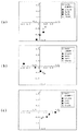
次に、実施例1において青色カラーフィルタ30Bに対するチヌビン123の添加量を変化させた場合の、L*a*b*表色系による有機ELディスプレイの物体色の評価結果を図5(a)に示す。なお、図5(a)においては、チヌビン123の添加量が0%の場合(すなわち、比較例1)も併せて示した。図5(a)から明らかなように、チヌビン123の添加量が5質量%までは、添加量の増大につれて、有機ELディスプレイの物体色が青方向(−b*方向)に移動することが分かる。また、チヌビン123の添加量が0〜5質量%の範囲においては、青色副画素を点灯させた場合の輝度および色度に実質的な変化は認められなかった。一方、チヌビン123の添加量を10質量%として場合には、物体色を変化させる効果がほとんど認められず、かつ青色カラーフィルタ30Bが白濁し、青色副画素を点灯させた場合の輝度が大きく低下した。これは、相分離剤40による光の散乱が過剰となったためと考えられる。
Next, FIG. 5A shows the evaluation results of the object color of the organic EL display using the L * a * b * color system when the amount of tinuvin 123 added to the
次に、実施例2において緑色カラーフィルタ30Gに対するチヌビン123の添加量を変化させた場合の有機ELディスプレイの物体色の評価結果を図5(b)に示す。この場合にも、チヌビン123の添加量の増大につれて、有機ELディスプレイの物体色が緑方向(−a*方向)に移動することを除いて、実施例1の場合と同様の評価結果が得られた。
Next, FIG. 5B shows the evaluation result of the object color of the organic EL display when the amount of tinuvin 123 added to the
さらに、実施例3において赤色カラーフィルタ30Rに対するチヌビン123の添加量を変化させた場合の有機ELディスプレイの物体色の評価結果を図5(c)に示す。この場合にも、チヌビン123の添加量の増大につれて有機ELディスプレイの物体色が赤方向(+a*方向)に移動することを除いて、実施例1の場合と同様の評価結果が得られた。
Furthermore, the evaluation result of the object color of the organic EL display when the amount of tinuvin 123 added to the
以上の検討結果から、各色のカラーフィルタ層に対して0〜5質量%の相分離剤を添加することによってカラーフィルタ層に入射する光の散乱量を独立的に制御し、点灯時の放射光の輝度および色度に影響を与えることなしに、非点灯時の有機ELディスプレイの物体色を調整できることが明らかとなった。 From the above examination results, the amount of light incident on the color filter layer is independently controlled by adding 0 to 5% by mass of a phase separating agent to each color filter layer, and the emitted light at the time of lighting is controlled. It has become clear that the object color of the organic EL display when not lit can be adjusted without affecting the brightness and chromaticity of the display.
10 透明基板
20 遮光層
30(R,G,B) カラーフィルタ層
40 相分離剤
50 平坦化層
60(R) 色変換層
70 ガスバリア層
80 透明電極
90 有機EL層
100 反射電極
DESCRIPTION OF
Claims (5)
Priority Applications (1)
| Application Number | Priority Date | Filing Date | Title |
|---|---|---|---|
| JP2007260003A JP2009087908A (en) | 2007-10-03 | 2007-10-03 | Organic el element |
Applications Claiming Priority (1)
| Application Number | Priority Date | Filing Date | Title |
|---|---|---|---|
| JP2007260003A JP2009087908A (en) | 2007-10-03 | 2007-10-03 | Organic el element |
Publications (1)
| Publication Number | Publication Date |
|---|---|
| JP2009087908A true JP2009087908A (en) | 2009-04-23 |
Family
ID=40661037
Family Applications (1)
| Application Number | Title | Priority Date | Filing Date |
|---|---|---|---|
| JP2007260003A Withdrawn JP2009087908A (en) | 2007-10-03 | 2007-10-03 | Organic el element |
Country Status (1)
| Country | Link |
|---|---|
| JP (1) | JP2009087908A (en) |
Cited By (2)
| Publication number | Priority date | Publication date | Assignee | Title |
|---|---|---|---|---|
| JP2014160644A (en) * | 2013-02-19 | 2014-09-04 | Au Optronics Corp | Color light emitting diode, display panel and method for manufacturing the same |
| WO2017057192A1 (en) * | 2015-09-30 | 2017-04-06 | 富士フイルム株式会社 | Resin film, colored photsensitive composition, resin film production method, color filter, light shielding film, solid-state imaging element, and image display device |
-
2007
- 2007-10-03 JP JP2007260003A patent/JP2009087908A/en not_active Withdrawn
Cited By (5)
| Publication number | Priority date | Publication date | Assignee | Title |
|---|---|---|---|---|
| JP2014160644A (en) * | 2013-02-19 | 2014-09-04 | Au Optronics Corp | Color light emitting diode, display panel and method for manufacturing the same |
| US9035286B2 (en) | 2013-02-19 | 2015-05-19 | Au Optronics Corporation | Multi-color light emitting diode and method for making same |
| WO2017057192A1 (en) * | 2015-09-30 | 2017-04-06 | 富士フイルム株式会社 | Resin film, colored photsensitive composition, resin film production method, color filter, light shielding film, solid-state imaging element, and image display device |
| JPWO2017057192A1 (en) * | 2015-09-30 | 2018-07-05 | 富士フイルム株式会社 | Resin film, colored photosensitive composition, resin film manufacturing method, color filter, light-shielding film, solid-state imaging device, and image display device |
| US10761251B2 (en) | 2015-09-30 | 2020-09-01 | Fujifilm Corporation | Resin film, coloring photosensitive composition, resin film production method, color filter, light shielding film, solid-state imaging element, and image display device |
Similar Documents
| Publication | Publication Date | Title |
|---|---|---|
| KR101237638B1 (en) | Color conversion film and multicolor emitting organic electroluminescent device comprising color conversion | |
| JP4756318B2 (en) | Color conversion filter and color conversion light emitting device using the same | |
| JP2007115419A (en) | Organic light emitting element | |
| GB2404276A (en) | Organic EL display | |
| JPWO2007055287A1 (en) | Organic EL display | |
| JPWO2006028089A1 (en) | Light emitting device and manufacturing method thereof | |
| WO2009098793A1 (en) | Organic el display and manufacturing method thereof | |
| JP4674524B2 (en) | Manufacturing method of organic EL light emitting display | |
| JP2006294454A (en) | Organic el element and its manufacturing method | |
| JP2009164117A (en) | Organic el device and method of manufacturing the same | |
| JP2010146760A (en) | Color conversion filter panel, panel type organic el emission portion, and color organic el display | |
| JP4618562B2 (en) | Manufacturing method of organic EL display | |
| JP2009129586A (en) | Organic el element | |
| JP2008103256A (en) | Organic el light emitting device, and its manufacturing method | |
| JP2009087908A (en) | Organic el element | |
| JP2009164049A (en) | Organic el device | |
| JP2009205929A (en) | Full-color organic el display panel | |
| JP2008305730A (en) | Manufacturing method for multicolor light-emitting device | |
| JP4699249B2 (en) | Color filter substrate for organic electroluminescence device | |
| JP2006261094A (en) | Color filter substrate for organic electroluminescent element | |
| JP3861821B2 (en) | Organic EL display panel and manufacturing method thereof | |
| JP5450738B2 (en) | Color conversion film and organic EL device including the color conversion film | |
| JP2008010417A (en) | Insulation film for organic el element and organic el display device | |
| JP2005196075A (en) | Color conversion type color display and control method for the color conversion type color display | |
| JP2008218344A (en) | Method of patterning color conversion layer and method of manufacturing organic el display |
Legal Events
| Date | Code | Title | Description |
|---|---|---|---|
| A761 | Written withdrawal of application |
Free format text: JAPANESE INTERMEDIATE CODE: A761 Effective date: 20091008 |