JP2009016571A - Semiconductor device - Google Patents
Semiconductor device Download PDFInfo
- Publication number
- JP2009016571A JP2009016571A JP2007176582A JP2007176582A JP2009016571A JP 2009016571 A JP2009016571 A JP 2009016571A JP 2007176582 A JP2007176582 A JP 2007176582A JP 2007176582 A JP2007176582 A JP 2007176582A JP 2009016571 A JP2009016571 A JP 2009016571A
- Authority
- JP
- Japan
- Prior art keywords
- layer
- region
- semiconductor device
- electrode
- trenches
- Prior art date
- Legal status (The legal status is an assumption and is not a legal conclusion. Google has not performed a legal analysis and makes no representation as to the accuracy of the status listed.)
- Granted
Links
- 239000004065 semiconductor Substances 0.000 title claims abstract description 151
- 238000009792 diffusion process Methods 0.000 claims description 14
- 230000000903 blocking effect Effects 0.000 claims description 6
- 239000010410 layer Substances 0.000 description 272
- 230000004888 barrier function Effects 0.000 description 31
- 239000011229 interlayer Substances 0.000 description 17
- 239000012535 impurity Substances 0.000 description 15
- 239000000758 substrate Substances 0.000 description 11
- XUIMIQQOPSSXEZ-UHFFFAOYSA-N Silicon Chemical compound [Si] XUIMIQQOPSSXEZ-UHFFFAOYSA-N 0.000 description 10
- 229910052710 silicon Inorganic materials 0.000 description 10
- 239000010703 silicon Substances 0.000 description 10
- 239000002184 metal Substances 0.000 description 8
- 230000000694 effects Effects 0.000 description 7
- 230000004048 modification Effects 0.000 description 5
- 238000012986 modification Methods 0.000 description 5
- VYPSYNLAJGMNEJ-UHFFFAOYSA-N Silicium dioxide Chemical compound O=[Si]=O VYPSYNLAJGMNEJ-UHFFFAOYSA-N 0.000 description 3
- 239000000969 carrier Substances 0.000 description 3
- 238000010586 diagram Methods 0.000 description 3
- 229910052814 silicon oxide Inorganic materials 0.000 description 3
- 230000015572 biosynthetic process Effects 0.000 description 2
- 238000004519 manufacturing process Methods 0.000 description 2
- 229910021420 polycrystalline silicon Inorganic materials 0.000 description 2
- 229920005591 polysilicon Polymers 0.000 description 2
- 239000003990 capacitor Substances 0.000 description 1
- 239000000470 constituent Substances 0.000 description 1
- 238000005530 etching Methods 0.000 description 1
- 230000005669 field effect Effects 0.000 description 1
- 238000009413 insulation Methods 0.000 description 1
- 239000000463 material Substances 0.000 description 1
- 229910044991 metal oxide Inorganic materials 0.000 description 1
- 150000004706 metal oxides Chemical class 0.000 description 1
- 230000001590 oxidative effect Effects 0.000 description 1
- 230000037361 pathway Effects 0.000 description 1
Images


Classifications
-
- H—ELECTRICITY
- H01—ELECTRIC ELEMENTS
- H01L—SEMICONDUCTOR DEVICES NOT COVERED BY CLASS H10
- H01L29/00—Semiconductor devices adapted for rectifying, amplifying, oscillating or switching, or capacitors or resistors with at least one potential-jump barrier or surface barrier, e.g. PN junction depletion layer or carrier concentration layer; Details of semiconductor bodies or of electrodes thereof ; Multistep manufacturing processes therefor
- H01L29/66—Types of semiconductor device ; Multistep manufacturing processes therefor
- H01L29/68—Types of semiconductor device ; Multistep manufacturing processes therefor controllable by only the electric current supplied, or only the electric potential applied, to an electrode which does not carry the current to be rectified, amplified or switched
- H01L29/76—Unipolar devices, e.g. field effect transistors
- H01L29/772—Field effect transistors
- H01L29/78—Field effect transistors with field effect produced by an insulated gate
- H01L29/7827—Vertical transistors
- H01L29/7828—Vertical transistors without inversion channel, e.g. vertical ACCUFETs, normally-on vertical MISFETs
-
- H—ELECTRICITY
- H01—ELECTRIC ELEMENTS
- H01L—SEMICONDUCTOR DEVICES NOT COVERED BY CLASS H10
- H01L29/00—Semiconductor devices adapted for rectifying, amplifying, oscillating or switching, or capacitors or resistors with at least one potential-jump barrier or surface barrier, e.g. PN junction depletion layer or carrier concentration layer; Details of semiconductor bodies or of electrodes thereof ; Multistep manufacturing processes therefor
- H01L29/66—Types of semiconductor device ; Multistep manufacturing processes therefor
- H01L29/68—Types of semiconductor device ; Multistep manufacturing processes therefor controllable by only the electric current supplied, or only the electric potential applied, to an electrode which does not carry the current to be rectified, amplified or switched
- H01L29/76—Unipolar devices, e.g. field effect transistors
- H01L29/772—Field effect transistors
- H01L29/78—Field effect transistors with field effect produced by an insulated gate
- H01L29/7839—Field effect transistors with field effect produced by an insulated gate with Schottky drain or source contact
Landscapes
- Engineering & Computer Science (AREA)
- Microelectronics & Electronic Packaging (AREA)
- Power Engineering (AREA)
- Physics & Mathematics (AREA)
- Ceramic Engineering (AREA)
- Condensed Matter Physics & Semiconductors (AREA)
- General Physics & Mathematics (AREA)
- Computer Hardware Design (AREA)
- Electrodes Of Semiconductors (AREA)
Abstract
Description
この発明は、半導体装置に関し、特に、スイッチング機能などを有する半導体装置に関する。 The present invention relates to a semiconductor device, and more particularly to a semiconductor device having a switching function.
従来、スイッチング機能を有する半導体装置として、MOSFET(Metal Oxide Semiconductor Field Effect Transistor)が知られている(たとえば、特許文献1参照)。この特許文献1には、半導体層に形成されたトレンチにゲート電極が埋め込まれたトレンチゲート型のMOSFET(半導体装置)が開示されている。
Conventionally, MOSFET (Metal Oxide Semiconductor Field Effect Transistor) is known as a semiconductor device having a switching function (see, for example, Patent Document 1). This
図19は、上記特許文献1に開示された従来のMOSFET(半導体装置)の構造を示した断面図である。図19を参照して、従来のMOSFET(半導体装置)では、n+型の半導体基板101の上面上に、エピタキシャル層(半導体層)102が形成されている。このエピタキシャル層102には、半導体基板101側から順に、n-型不純物領域(ドレイン領域)102a、p型不純物領域102bおよびn+型不純物領域(ソース領域)102cが形成されている。
FIG. 19 is a cross-sectional view showing the structure of a conventional MOSFET (semiconductor device) disclosed in
また、エピタキシャル層102には、n+型不純物領域102cおよびp型不純物領域102bを貫通してn-型不純物領域102aの途中の深さにまで達するトレンチ103が形成されている。このトレンチ103には、ゲート絶縁膜104を介して、ゲート電極105が埋め込まれている。また、エピタキシャル層102の上面上には、トレンチ103の開口端を塞ぐ層間絶縁膜106が形成されている。
In addition,
また、エピタキシャル層102の上面上には、層間絶縁膜106を覆うように、ソース電極107が形成されている。また、半導体基板101の裏面上には、ドレイン電極108が形成されている。
A
上記のように構成された従来のMOSFETでは、ゲート電極105に対する印加電圧を変化させることによりオン/オフの制御が行われる。
In the conventional MOSFET configured as described above, ON / OFF control is performed by changing the voltage applied to the
具体的には、ゲート電極105に対して所定の正電位を印加すると、p型不純物領域102bの少数キャリア(電子)がトレンチ103側に引き寄せられることによって、n-型不純物領域(ドレイン領域)102aとn+型不純物領域(ソース領域)102cとを接続するような反転層109が形成される。これにより、反転層109を介して、ソース電極107とドレイン電極108との間に電流を流すことができる。その結果、MOSFETがオン状態となる。
Specifically, when a predetermined positive potential is applied to the
このように、従来のMOSFETでは、n-型不純物領域(ドレイン領域)102aとn+型不純物領域(ソース領域)102cとを接続するように形成される反転層109をチャネルとして機能させている。
Thus, in the conventional MOSFET, the
また、上記した状態からゲート電極105に対する所定の正電位の印加を解除すると、反転層(チャネル)109が消滅するので、ソース電極107とドレイン電極108との間に流れる電流を遮断することができる。その結果、MOSFETがオフ状態となる。
Further, when the application of a predetermined positive potential to the
しかしながら、図19に示した従来の構造では、オン時に形成される反転層(チャネル)109が非常に薄いため、反転層(チャネル)109を流れる電流に対する抵抗を低減するのが困難であるという不都合がある。その結果、オン抵抗の改善を図るのが困難であるという問題点がある。 However, in the conventional structure shown in FIG. 19, since the inversion layer (channel) 109 formed at the time of ON is very thin, it is difficult to reduce the resistance to the current flowing through the inversion layer (channel) 109. There is. As a result, there is a problem that it is difficult to improve the on-resistance.
この発明は、上記のような課題を解決するためになされたものであり、この発明の目的は、オン抵抗を大幅に低減することが可能な新しい動作原理に基づく半導体装置を提供することである。 The present invention has been made to solve the above-described problems, and an object of the present invention is to provide a semiconductor device based on a new operating principle capable of greatly reducing the on-resistance. .
上記目的を達成するために、この発明の一の局面による半導体装置は、互いに所定の間隔を隔てて配列され、かつ、各々の開口端が上面側に位置している複数のトレンチを有する一導電型の半導体層と、複数のトレンチの各々に埋め込まれた複数の埋め込み電極と、半導体層の上面上に形成された電極層とを備えている。そして、半導体層の隣接するトレンチ間の各領域が電流通路となり、かつ、トレンチの周辺に形成される空乏層で半導体層の隣接するトレンチ間の各領域が塞がれることにより電流通路が遮断される一方、トレンチの周辺に形成された空乏層の少なくとも一部が消滅することにより電流通路が開くように構成されており、半導体層の隣接するトレンチ間の各領域のうちの所定領域の上面は、電極層に対してショットキー接触している。 In order to achieve the above object, a semiconductor device according to an aspect of the present invention includes a plurality of trenches arranged at predetermined intervals from each other and having a plurality of trenches, each open end being located on the upper surface side. A semiconductor layer of a type, a plurality of embedded electrodes embedded in each of the plurality of trenches, and an electrode layer formed on the upper surface of the semiconductor layer. Each region between adjacent trenches in the semiconductor layer serves as a current path, and the current path is blocked by blocking each region between adjacent trenches in the semiconductor layer with a depletion layer formed around the trench. On the other hand, the current path is configured to be opened when at least part of the depletion layer formed around the trench disappears, and the upper surface of a predetermined region of each region between adjacent trenches of the semiconductor layer is The Schottky contact is made to the electrode layer.
この一の局面による半導体装置では、上記のように、トレンチの周辺に形成される空乏層で半導体層の隣接するトレンチ間の各領域が塞がれることにより電流通路(半導体層の隣接するトレンチ間の各領域)が遮断される一方、トレンチの周辺に形成された空乏層の少なくとも一部が消滅することにより電流通路(半導体層の隣接するトレンチ間の各領域)が開くように構成することによって、たとえば、トレンチの内面上に絶縁膜を介して埋め込み電極を形成すれば、その埋め込み電極に対する印加電圧に応じてトレンチの周辺に形成される空乏層の形成状態が変化するので、埋め込み電極に対する印加電圧を制御することにより、オン状態(電流通路が開いている状態)からオフ状態(電流通路が遮断されている状態)への切り替えを行うことができるとともに、その逆の切り替えも行うことができる。すなわち、半導体装置をスイッチ装置(スイッチングトランジスタ)として用いることができる。そして、上記した構成では、オン時において、電流通路(半導体層の隣接するトレンチ間の各領域)の空乏層が消滅した部分の全てを介して電流を流すことができるので、非常に薄い反転層をチャネル(電流通路)として機能させる従来のMOSFET(半導体装置)と比べて、電流に対する抵抗を大幅に低減することが可能となる。これにより、非常に薄い反転層をチャネル(電流通路)として機能させる従来のMOSFET(半導体装置)と比べて、オン抵抗を大幅に低減することができる。 In the semiconductor device according to this aspect, as described above, each region between adjacent trenches of the semiconductor layer is blocked by a depletion layer formed around the trench, thereby causing a current path (between adjacent trenches of the semiconductor layer). The current path (each region between adjacent trenches in the semiconductor layer) is opened when at least part of the depletion layer formed around the trench disappears. For example, if a buried electrode is formed on the inner surface of a trench through an insulating film, the formation state of a depletion layer formed around the trench changes according to the voltage applied to the buried electrode, so that the application to the buried electrode By controlling the voltage, switching from the on state (the current path is open) to the off state (the current path is blocked) is performed. It is possible, can also switches the reverse. That is, the semiconductor device can be used as a switch device (switching transistor). In the above-described configuration, since the current can flow through all the portions where the depletion layer of the current path (each region between adjacent trenches of the semiconductor layer) disappears at the time of ON, a very thin inversion layer As compared with a conventional MOSFET (semiconductor device) that functions as a channel (current path), the resistance to current can be greatly reduced. As a result, the on-resistance can be greatly reduced as compared with a conventional MOSFET (semiconductor device) in which a very thin inversion layer functions as a channel (current path).
また、一の局面による半導体装置では、上記のように、半導体層の隣接するトレンチ間の各領域のうちの所定領域の上面が、電極層に対してショットキー接触するように構成することによって、半導体層の隣接するトレンチ間の各領域のうちの所定領域と電極層との接触部分をショットキーバリアダイオードとして機能させることができるので、ショットキーバリアダイオードとスイッチングトランジスタとを一体化することが可能となる。これにより、ショットキーバリアダイオードとスイッチングトランジスタとを接続するための配線部材の形成領域などを別途設ける必要がなくなるので、互いに接続されるショットキーバリアダイオードおよびスイッチングトランジスタを含む回路の小面積化を図ることができる。 Further, in the semiconductor device according to one aspect, as described above, the upper surface of the predetermined region of each region between adjacent trenches of the semiconductor layer is configured to be in Schottky contact with the electrode layer. A contact portion between a predetermined region of each region between adjacent trenches of the semiconductor layer and the electrode layer can function as a Schottky barrier diode, so that the Schottky barrier diode and the switching transistor can be integrated. It becomes. This eliminates the need to separately provide a wiring member forming region for connecting the Schottky barrier diode and the switching transistor, thereby reducing the area of the circuit including the Schottky barrier diode and the switching transistor connected to each other. be able to.
また、上記した構成では、トレンチの周辺に形成される空乏層で半導体層の隣接するトレンチ間の各領域を塞ぐことができるので、半導体層の隣接するトレンチ間の各領域のうちの所定領域と電極層との接合部分(ショットキー接触している部分)を空乏層で塞ぐことが可能となる。これにより、ショットキーバリアダイオードにおけるリーク電流の発生を抑制することができる。 In the above-described configuration, each region between adjacent trenches in the semiconductor layer can be blocked with a depletion layer formed around the trench. It becomes possible to block the junction with the electrode layer (the part in Schottky contact) with the depletion layer. Thereby, generation | occurrence | production of the leakage current in a Schottky barrier diode can be suppressed.
上記一の局面による半導体装置において、好ましくは、電極層は、半導体層の隣接するトレンチ間の各領域のうちの所定領域の上面に対してショットキー接触する第1部分と、半導体層の隣接するトレンチ間の各領域のうちの所定領域以外の領域の上面に対してオーミック接触する第2部分とを含んでいる。このように構成すれば、電極層の第1部分および第2部分を互いに電気的に分離することにより、スイッチングトランジスタのソース/ドレイン電極の一方とショットキーバリアダイオードのアノードとが電気的に分離された回路を得ることができる。その一方、電極層の第1部分および第2部分を互いに電気的に接続すれば、スイッチングトランジスタのソース/ドレイン電極の一方とショットキーバリアダイオードのアノードとが電気的に接続された回路を得ることができる。 In the semiconductor device according to the above aspect, preferably, the electrode layer is adjacent to the first portion in Schottky contact with the upper surface of a predetermined region of each region between adjacent trenches of the semiconductor layer, and the semiconductor layer. And a second portion in ohmic contact with the upper surface of the region other than the predetermined region among the regions between the trenches. With this configuration, by electrically separating the first and second portions of the electrode layer from each other, one of the source / drain electrodes of the switching transistor and the anode of the Schottky barrier diode are electrically separated. Circuit can be obtained. On the other hand, if the first part and the second part of the electrode layer are electrically connected to each other, a circuit in which one of the source / drain electrodes of the switching transistor and the anode of the Schottky barrier diode are electrically connected can be obtained. Can do.
上記電極層が第1部分と第2部分とを含む構成において、電極層の第1部分および電極層の第2部分は、互いに電気的に分離されていてもよい。このように構成すれば、スイッチングトランジスタのソース/ドレイン電極の一方とショットキーバリアダイオードのアノードとが電気的に分離された回路を容易に得ることができる。 In the configuration in which the electrode layer includes the first portion and the second portion, the first portion of the electrode layer and the second portion of the electrode layer may be electrically separated from each other. With this configuration, it is possible to easily obtain a circuit in which one of the source / drain electrodes of the switching transistor and the anode of the Schottky barrier diode are electrically separated.
上記電極層が第1部分と第2部分とを含む構成において、電極層の第1部分および電極層の第2部分は、互いに電気的に接続されていてもよい。このように構成すれば、スイッチングトランジスタのソース/ドレイン電極の一方とショットキーバリアダイオードのアノードとが電気的に接続された回路を容易に得ることができる。 In the configuration in which the electrode layer includes the first portion and the second portion, the first portion of the electrode layer and the second portion of the electrode layer may be electrically connected to each other. With this configuration, a circuit in which one of the source / drain electrodes of the switching transistor and the anode of the Schottky barrier diode are electrically connected can be easily obtained.
上記一の局面による半導体装置において、好ましくは、電極層に対してショットキー接触する半導体層の所定領域は、半導体層の隣接するトレンチ間の各領域に少なくとも1つずつ設けられている。このように構成すれば、容易に、ショットキーバリアダイオードとスイッチングトランジスタとを一体化することができる。 In the semiconductor device according to the above aspect, at least one predetermined region of the semiconductor layer that is in Schottky contact with the electrode layer is provided in each region between adjacent trenches of the semiconductor layer. If comprised in this way, a Schottky barrier diode and a switching transistor can be integrated easily.
この場合、半導体層の隣接するトレンチ間の各領域に、電極層に対してショットキー接触する所定領域と、電極層に対してショットキー接触する所定領域以外の領域とが1つずつ交互に設けられていることが好ましい。 In this case, in each region between adjacent trenches of the semiconductor layer, a predetermined region that makes a Schottky contact with the electrode layer and a region other than the predetermined region that makes a Schottky contact with the electrode layer are alternately provided. It is preferable that
上記一の局面による半導体装置において、複数のトレンチの各々の周辺に形成される全ての空乏層で隣接するトレンチ間の各領域が塞がれることにより電流通路が遮断される一方、複数のトレンチの各々の周辺に形成された全ての空乏層が消滅することにより電流通路が開くように構成されていてもよい。 In the semiconductor device according to the above aspect, the current path is blocked by blocking each region between adjacent trenches in all the depletion layers formed around each of the plurality of trenches. The current path may be opened when all the depletion layers formed around each of them disappear.
上記一の局面による半導体装置において、複数の埋め込み電極は、互いに別個に電圧が印加される第1埋め込み電極および第2埋め込み電極の2種類に分けられており、複数のトレンチのうちの全てのトレンチの周辺に形成される空乏層で隣接するトレンチ間の各領域が塞がれることにより電流通路が遮断される一方、複数のトレンチのうちの第1埋め込み電極が埋め込まれたトレンチの周辺に形成された空乏層が消滅することにより電流通路が開くように構成されていてもよい。 In the semiconductor device according to the above aspect, the plurality of embedded electrodes are divided into two types, a first embedded electrode and a second embedded electrode to which a voltage is separately applied, and all of the plurality of trenches A current path is blocked by blocking each region between adjacent trenches with a depletion layer formed at the periphery of the trench, while the first buried electrode of the plurality of trenches is formed around the trench embedded therein. Alternatively, the current path may be opened when the depletion layer disappears.
この場合、第2埋め込み電極は、トレンチの内部において、半導体層に対してショットキー接触していてもよい。 In this case, the second embedded electrode may be in Schottky contact with the semiconductor layer inside the trench.
上記一の局面による半導体装置において、半導体層の隣接するトレンチ間の各領域に形成され、トレンチに対して所定の間隔を隔てて配置された逆導電型の拡散層をさらに備え、トレンチおよび拡散層の各々の周辺に形成される空乏層で隣接するトレンチ間の各領域が塞がれることにより電流通路が遮断される一方、トレンチの周辺に形成された空乏層が消滅することにより電流通路が開くように構成されていてもよい。 In the semiconductor device according to the above aspect, the semiconductor device further includes a reverse conductivity type diffusion layer formed in each region between adjacent trenches of the semiconductor layer and disposed at a predetermined interval with respect to the trench, the trench and the diffusion layer Each of the regions between adjacent trenches is blocked by a depletion layer formed around each of the trenches, while the current path is blocked, while the depletion layer formed around the trenches disappears to open the current pathway. It may be configured as follows.
なお、上記一の局面による半導体装置において、半導体層の隣接するトレンチ間の各領域を介して流れる電流を遮断する場合に、隣接するトレンチの各々の周辺に形成される空乏層が互いに連結された状態になるように構成されていてもよい。このように構成すれば、確実に、半導体層の隣接するトレンチ間の各領域を空乏層で塞ぐことができる。 In the semiconductor device according to the above aspect, when the current flowing through each region between adjacent trenches of the semiconductor layer is cut off, the depletion layers formed around each of the adjacent trenches are connected to each other. You may be comprised so that it may be in a state. If comprised in this way, each area | region between the adjacent trenches of a semiconductor layer can be reliably block | closed with a depletion layer.
また、上記一の局面による半導体装置において、隣接するトレンチ間の距離は、隣接するトレンチの各々の周辺に形成される空乏層の一部が互いに重なるように設定されていてもよい。このように構成すれば、容易に、隣接するトレンチの各々の周辺に形成される空乏層を互いに連結させることができる。 In the semiconductor device according to the above aspect, the distance between adjacent trenches may be set such that a part of depletion layers formed around each adjacent trench overlap each other. If comprised in this way, the depletion layer formed in the circumference | surroundings of each adjacent trench can be connected mutually easily.
また、上記一の局面による半導体装置において、埋め込み電極と電極層との間の絶縁を行うための層間絶縁膜をさらに備え、埋め込み電極は、トレンチの途中の深さまでを埋め込んでおり、層間絶縁膜は、層間絶縁膜の上面が半導体層の上面に対して面一となるように、トレンチの埋め込み電極が埋め込まれていない残りの部分に埋め込まれていてもよい。このように構成すれば、隣接するトレンチ間の距離を小さくしたとしても、半導体層の上面側の部分(半導体層の隣接するトレンチ間の領域の上端部)が層間絶縁膜で覆われてしまうことがない。これにより、隣接するトレンチ間の距離を小さくすることができるので、隣接するトレンチの各々の周辺に形成される空乏層を互いに連結させやすくすることが可能となる。 The semiconductor device according to one aspect further includes an interlayer insulating film for performing insulation between the buried electrode and the electrode layer, and the buried electrode is buried to a depth in the middle of the trench, and the interlayer insulating film May be buried in the remaining portion of the trench where the buried electrode is not buried so that the upper surface of the interlayer insulating film is flush with the upper surface of the semiconductor layer. With this configuration, even if the distance between adjacent trenches is reduced, the upper surface side portion of the semiconductor layer (the upper end portion of the region between adjacent trenches of the semiconductor layer) is covered with the interlayer insulating film. There is no. Thereby, since the distance between adjacent trenches can be reduced, depletion layers formed around each of adjacent trenches can be easily connected to each other.
以上のように、本発明によれば、オン抵抗を大幅に低減することが可能な新しい動作原理に基づく半導体装置を容易に得ることができる。 As described above, according to the present invention, it is possible to easily obtain a semiconductor device based on a new operation principle capable of greatly reducing the on-resistance.
(第1実施形態)
図1は、本発明の第1実施形態による半導体装置を示した断面斜視図である。図2は、図1に示した第1実施形態による半導体装置の埋め込み電極の接続位置を説明するための断面図である。図3は、図1に示した第1実施形態による半導体装置の等価回路である。まず、図1〜図3を参照して、第1実施形態による半導体装置の構造について説明する。
(First embodiment)
FIG. 1 is a cross-sectional perspective view showing a semiconductor device according to a first embodiment of the present invention. FIG. 2 is a cross-sectional view for explaining the connection position of the buried electrode of the semiconductor device according to the first embodiment shown in FIG. FIG. 3 is an equivalent circuit of the semiconductor device according to the first embodiment shown in FIG. First, the structure of the semiconductor device according to the first embodiment will be described with reference to FIGS.
第1実施形態による半導体装置11は、図1に示すように、ノーマリオフ型のスイッチングトランジスタとして機能する領域と、ショットキーバリアダイオードとして機能する領域とが一体的に設けられた構造を有している。
As shown in FIG. 1, the
具体的な構造としては、第1実施形態による半導体装置11では、n+型シリコン基板1の上面上に、約1μm〜約10μmの厚みを有するn型シリコンからなるn型エピタキシャル層2が形成されている。n+型シリコン基板1には、後述する裏面電極層8との間で良好なオーミック接触を得るために、n型不純物が高濃度で導入されている。また、n型エピタキシャル層2には、n型不純物がn+型シリコン基板1よりも低い濃度(約5×1015cm-3〜約1×1018cm-3)で導入されている。なお、n+型シリコン基板1およびn型エピタキシャル層2は、本発明の「一導電型の半導体層」の一例である。
As a specific structure, in the
また、n型エピタキシャル層2は、その厚み方向に掘られた複数のトレンチ3を有している。この複数のトレンチ3は、n型エピタキシャル層2をその上面(主表面)側からエッチングすることによって形成されている。すなわち、複数のトレンチ3の各々の開口端は、n型エピタキシャル層2の上面側に位置している。
The n-
また、複数のトレンチ3は、その各々がn型エピタキシャル層2の上面に対して平行な所定方向(A方向)に沿って延びるように細長状に形成されている。また、複数のトレンチ3は、n型エピタキシャル層2の上面に対して平行で、かつ、トレンチ3が延びる方向(A方向)と直交する方向(B方向)に互いに約0.05μm〜約0.3μmの間隔を隔てて配列されている。さらに、複数のトレンチ3の各々の溝深さは、約0.5μm〜約12μmに設定されている。この第1実施形態のトレンチ3の溝深さは、n型エピタキシャル層2の厚み(約1μm〜約10μm)よりも小さくなるように設定されている。なお、図示しないが、トレンチ3がn型エピタキシャル層2を貫通してn+型シリコン基板1にまで達していてもよい。また、複数のトレンチ3の各々のB方向の幅は、約0.1μm〜約1μmに設定されている。
The plurality of
また、複数のトレンチ3の各々の内面上には、n型エピタキシャル層2を構成するシリコンを熱酸化処理することによって得られるシリコン酸化膜(絶縁膜)4が約10nm〜約100nmの厚みで形成されている。
A silicon oxide film (insulating film) 4 obtained by thermally oxidizing silicon constituting the n-
また、複数のトレンチ3の各々の内面上には、シリコン酸化膜4を介して、p型ポリシリコンからなる埋め込み電極5が形成されている。この複数の埋め込み電極5の各々は、対応するトレンチ3の途中の深さまでを埋め込んでいる。なお、埋め込み電極5の構成材料としては、p型ポリシリコン以外に、金属などを用いることもできる。
A buried
上記のような複数の埋め込み電極5を設けた第1実施形態では、複数の埋め込み電極5に対する印加電圧を制御すれば、複数のトレンチ3の各々の周辺に空乏層を形成したり、その形成された空乏層を消滅させたりすることが可能となる。そして、第1実施形態では、隣接するトレンチ3間の距離は、複数のトレンチ3の各々の周辺に空乏層を形成した時に、隣接するトレンチ3の各々の周辺に形成された空乏層の一部が互いに重なるように設定されている。すなわち、複数のトレンチ3の各々の周辺に空乏層を形成した場合には、隣接するトレンチ3の各々の周辺に形成された空乏層が互いに連結される。このため、第1実施形態では、複数のトレンチ3の各々の周辺に空乏層を形成すれば、n型エピタキシャル層2の隣接するトレンチ3間の各領域が空乏層によって塞がれた状態にすることができる。
In the first embodiment in which the plurality of embedded
また、複数のトレンチ3の各々の埋め込み電極5が埋め込まれていない残りの部分(埋め込み電極5よりも上方の部分)には、シリコン酸化膜からなる層間絶縁膜6が埋め込まれている。この複数の層間絶縁膜6の各々は、対応する埋め込み電極5と後述する上面電極層7との間で絶縁を行うために設けられている。また、複数の層間絶縁膜6の各々の厚みは、対応するトレンチ3の埋め込み電極5が埋め込まれていない残りの部分(埋め込み電極5よりも上方の部分)の深さと同じになるように設定されている。したがって、複数の層間絶縁膜6の各々の上面は、n型エピタキシャル層2の上面(隣接するトレンチ3間の各領域の上端部の上面)に対して面一となっている。
An interlayer insulating
また、n型エピタキシャル層2の上面側の部分(隣接するトレンチ3間の各領域の上端部)には、A方向に沿って互いに所定の間隔を隔てて配置された複数の高濃度領域2aが形成されている。このn型エピタキシャル層2の高濃度領域2aの濃度は、n型エピタキシャル層2の他の部分の濃度よりも高くなっている。すなわち、n型エピタキシャル層2の上面側の部分(隣接するトレンチ3間の各領域の上端部)には、高濃度領域2aと低濃度領域とがA方向に沿って1ずつ交互に設けられていることになる。さらに、n型エピタキシャル層2の高濃度領域2aの厚みは、層間絶縁膜6の厚みよりも小さくなるように設定されている。このため、n型エピタキシャル層2の高濃度領域2aの下端部は、埋め込み電極5の上端部よりも上方に位置していることになる。
A plurality of high-
また、n型エピタキシャル層2の上面上には、金属層(たとえば、Al層)からなるとともに、部分7aおよび7bを所定数ずつ含む上面電極層7が形成されている。この上面電極層7の部分7aおよび7bは、互いに電気的に分離されている。さらに、上面電極層7の部分7aおよび7bは、B方向に沿って延びるように細長状に形成されているとともに、A方向に1つずつ交互に配置されている。なお、上面電極層7は、本発明の「電極層」の一例である。また、部分7aおよび7bは、それぞれ、本発明の「第2部分」および「第1部分」の一例である。
On the upper surface of n-
そして、上面電極層7の部分7aは、スイッチングトランジスタのソース電極として機能するように、n型エピタキシャル層2の高濃度領域2aに対してオーミック接触している。その一方、上面電極層7の部分7bは、n型エピタキシャル層2の低濃度領域に対してショットキー接触している。すなわち、上面電極層7の部分7bとn型エピタキシャル層2の低濃度領域との接合部分は、ショットキーバリアダイオードとして機能することになる。この場合、上面電極層7の部分7bがショットキーバリアダイオードのアノードとなり、n型エピタキシャル層2の低濃度領域がショットキーバリアダイオードのカソードとなる。
The
また、n+型シリコン基板1の裏面上には、複数の金属層が積層された多層構造の裏面電極層8が形成されている。この裏面電極層8は、n+型シリコン基板1に対してオーミック接触している。そして、裏面電極層8は、スイッチングトランジスタのドレイン電極として機能する。
Further, on the back surface of the n + -
上記した構成では、上面電極層7と裏面電極層8との間を流れる電流(n型エピタキシャル層2の厚み方向に流れる電流)は、n型エピタキシャル層2の隣接するトレンチ3間の各領域を通過することになる。すなわち、上記した構成では、n型エピタキシャル層2の隣接するトレンチ3間の各領域が電流通路9として機能することになる。
In the configuration described above, the current flowing between the
ところで、第1実施形態では、複数の埋め込み電極5は、互いに別個に電圧が印加される2種類の埋め込み電極5aおよび5bに分けられている。具体的には、図2に示すように、埋め込み電極5aは、所定の制御信号(オン/オフの切り替えを行うための信号)に対応する電圧が印加されるように構成されている。その一方、埋め込み電極5bは、上面電極層7の部分(ソース電極)7aに電気的に接続されている。すなわち、埋め込み電極5bは、上面電極層7の部分(ソース電極)7aと同電位となるように構成されている。なお、埋め込み電極5aおよび5bは、それぞれ、本発明の「第1埋め込み電極」および「第2埋め込み電極」の一例である。
Incidentally, in the first embodiment, the plurality of embedded
また、第1実施形態では、埋め込み電極5aおよび5bは、B方向に1つずつ交互に配置されている。すなわち、2つの埋め込み電極5a(5b)の間に1つの埋め込み電極5b(5a)が配置されていることになる。
In the first embodiment, the embedded
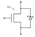
上記した第1実施形態の半導体装置11は、図3に示すような等価回路で表すことができる。すなわち、第1実施形態の半導体装置11では、図3に示すように、スイッチングトランジスタのソースとショットキーバリアダイオードのカソードとが互いに電気的に接続された回路となる。なお、図3では、便宜上、半導体装置11のスイッチングトランジスタの部分をMOSFETの回路記号で表している。
The
図4および図5は、本発明の第1実施形態による半導体装置の動作を説明するための断面図である。図4には、半導体装置(スイッチングトランジスタ)がオフ状態となっている場合を図示しており、図5には、半導体装置(スイッチングトランジスタ)がオン状態となっている場合を図示している。次に、図4および図5を参照して、第1実施形態による半導体装置の動作について説明する。 4 and 5 are cross-sectional views for explaining the operation of the semiconductor device according to the first embodiment of the present invention. FIG. 4 illustrates the case where the semiconductor device (switching transistor) is in an off state, and FIG. 5 illustrates the case where the semiconductor device (switching transistor) is in an on state. Next, the operation of the semiconductor device according to the first embodiment will be described with reference to FIGS.
まず、図4および図5に示すように、上面電極層7の部分(ソース電極)7aおよび裏面電極層(ドレイン電極)8の各々に負電位および正電位が印加されているとすると、埋め込み電極5bが上面電極層7の部分(ソース電極)7aに電気的に接続されているため、埋め込み電極5bに対して負電位が印加されることになる。したがって、埋め込み電極5bが埋め込まれたトレンチ3(以下、トレンチ3bと言う)の周辺は、多数キャリアが減少した状態となっている。すなわち、トレンチ3bの周辺には、オン状態およびオフ状態にかかわらず、空乏層10(10b)が形成されている。
First, as shown in FIGS. 4 and 5, assuming that a negative potential and a positive potential are applied to each of the
そして、図4に示すように、半導体装置(スイッチングトランジスタ)11がオフ状態の場合には、埋め込み電極5aが埋め込まれたトレンチ3(以下、トレンチ3aと言う)の周辺に存在する多数キャリアが減少するように、埋め込み電極5aに対する印加電圧が制御されている。これにより、トレンチ3aの周辺には、トレンチ3bの周辺に形成された空乏層10bと同様の空乏層10(10a)が形成されている。
As shown in FIG. 4, when the semiconductor device (switching transistor) 11 is in an off state, the majority carriers existing around the
この際、トレンチ3aとトレンチ3bとの間の領域では、トレンチ3aおよび3bの各々の周辺に形成された空乏層10aおよび10bの一部が互いに重なる。すなわち、トレンチ3aとトレンチ3bとの間の領域では、空乏層10aおよび10bが互いに連結された状態となる。これにより、電流通路9が空乏層10aおよび10bによって塞がれた状態となるので、電流通路9を介して流れる電流を遮断することができる。したがって、半導体装置(スイッチングトランジスタ)11がオフ状態となる。
At this time, in the region between the
次に、図5に示すように、半導体装置(スイッチングトランジスタ)11をオフ状態からオン状態に切り替える場合には、埋め込み電極5aに対して所定の正電位を印加することによって、トレンチ3aの周辺に形成された空乏層10a(図4参照)を消滅させる。すなわち、電流通路9の埋め込み電極5a側の部分を塞いでいた空乏層10aを消滅させる。これにより、電流通路9の埋め込み電極5a側の部分を介して図5中の矢印方向に電流を流すことができるので、半導体装置(スイッチングトランジスタ)11をオン状態にすることが可能となる。
Next, as shown in FIG. 5, when the semiconductor device (switching transistor) 11 is switched from the off state to the on state, a predetermined positive potential is applied to the embedded
また、半導体装置(スイッチングトランジスタ)11をオン状態からオフ状態に切り替える場合には、埋め込み電極5aに対する所定の正電位の印加を解除する。これにより、図4に示した状態に戻るので、半導体装置(スイッチングトランジスタ)11をオフ状態にすることが可能となる。
When the semiconductor device (switching transistor) 11 is switched from the on state to the off state, the application of a predetermined positive potential to the embedded
第1実施形態では、上記のように、トレンチ3の周辺に形成される空乏層10でn型エピタキシャル層2の隣接するトレンチ3間の各領域が塞がれることにより、n型エピタキシャル層2の隣接するトレンチ3間の各領域を介して流れる電流が遮断される一方、トレンチ3の周辺に形成された空乏層10の少なくとも一部(トレンチ3aの周辺に形成された空乏層10a)が消滅することにより、n型エピタキシャル層2の隣接するトレンチ3間の各領域を介して電流が流れるように構成することによって、トレンチ3の周辺に形成される空乏層10の形成状態は埋め込み電極5に対する印加電圧に応じて変化するので、埋め込み電極5に対する印加電圧を制御することにより、オン状態(n型エピタキシャル層2の隣接するトレンチ3間の各領域を介して電流が流れる状態)からオフ状態(n型エピタキシャル層2の隣接するトレンチ3間の各領域を介して流れる電流が遮断される状態)への切り替えを行うことができるとともに、その逆の切り替えも行うことができる。すなわち、半導体装置11をスイッチ装置(スイッチングトランジスタ)として用いることができる。そして、上記した構成では、オン時において、n型エピタキシャル層2の隣接するトレンチ3間の各領域の空乏層10が消滅した部分の全てを電流通路9として機能させることができるので、非常に薄い反転層をチャネル(電流通路)として機能させる従来のMOSFET(半導体装置)と比べて、電流に対する抵抗を大幅に低減することが可能となる。これにより、非常に薄い反転層をチャネル(電流通路)として機能させる従来のMOSFET(半導体装置)と比べて、オン抵抗を大幅に低減することができる。
In the first embodiment, as described above, each region between the
また、第1実施形態では、上記のように、n型エピタキシャル層2の隣接するトレンチ3間の各領域のうちの所定領域の上面が、上面電極層7に対してショットキー接触するように構成することによって、n型エピタキシャル層2の隣接するトレンチ3間の各領域のうちの所定領域と上面電極層7との接触部分をショットキーバリアダイオードとして機能させることができるので、ショットキーバリアダイオードとスイッチングトランジスタとを一体化することが可能となる。これにより、ショットキーバリアダイオードとスイッチングトランジスタとを接続するための配線部材の形成領域などを別途設ける必要がなくなるので、互いに接続されるショットキーバリアダイオードおよびスイッチングトランジスタを含む回路の小面積化を図ることができる。
Further, in the first embodiment, as described above, the upper surface of a predetermined region in each region between
また、上記した構成では、トレンチ3の周辺に形成される空乏層10でn型エピタキシャル層2の隣接するトレンチ3間の各領域を塞ぐことができるので、n型エピタキシャル層2の隣接するトレンチ3間の各領域のうちの所定領域と上面電極層7との接合部分(ショットキー接触している部分)を空乏層10で塞ぐことが可能となる。これにより、ショットキーバリアダイオードにおけるリーク電流の発生を抑制することができる。
Further, in the above-described configuration, each region between the
また、第1実施形態では、上記のように、上面電極層7の部分7aおよび7bを、互いに電気的に分離することによって、スイッチングトランジスタのソース/ドレイン電極の一方とショットキーバリアダイオードのアノードとが電気的に分離された回路を容易に得ることができる。この場合、半導体装置11をDC/DCコンバータを構成する部品の一部として用いることができる(図6および図7参照)。なお、図6に示すDC/DCコンバータは降圧型であり、図7に示すDC/DCコンバータは昇降圧型である。また、図6および図7の符号31は、コイルである。
In the first embodiment, as described above, the
また、第1実施形態では、上記のように、オフ時において、隣接するトレンチ3の各々の周辺に形成された空乏層10が互いに連結された状態になるように構成することによって、確実に、電流通路(n型エピタキシャル層2の隣接するトレンチ3間の各領域)9を空乏層10で塞ぐことができる。
In the first embodiment, as described above, the
また、第1実施形態では、上記のように、隣接するトレンチ3間の距離を、隣接するトレンチ3の各々の周辺に形成された空乏層10の一部が互いに重なるように設定することによって、容易に、隣接するトレンチ3の各々の周辺に形成された空乏層10を互いに連結させることができる。
In the first embodiment, as described above, the distance between the
また、第1実施形態では、上記のように、層間絶縁膜6の上面がn型エピタキシャル層2の上面に対して面一となるように、層間絶縁膜6をトレンチ3に埋め込むことによって、隣接するトレンチ3間の距離を小さくしたとしても、n型エピタキシャル層2の上面側の部分(隣接するトレンチ3間の領域の上端部)が層間絶縁膜6で覆われてしまうことがない。これにより、隣接するトレンチ3間の距離を小さくすることができるので、隣接するトレンチ3の各々の周辺に形成された空乏層10を互いに連結させやすくすることができる。
In the first embodiment, as described above, the
(第2実施形態)
図8は、本発明の第2実施形態による半導体装置を示した断面斜視図である。図9は、図8に示した第2実施形態による半導体装置の埋め込み電極の接続位置を説明するための断面図である。図10は、図8に示した第2実施形態による半導体装置の等価回路である。次に、図8〜図10を参照して、第2実施形態による半導体装置の構造について説明する。
(Second Embodiment)
FIG. 8 is a cross-sectional perspective view showing a semiconductor device according to the second embodiment of the present invention. FIG. 9 is a cross-sectional view for explaining the connection position of the buried electrode of the semiconductor device according to the second embodiment shown in FIG. FIG. 10 is an equivalent circuit of the semiconductor device according to the second embodiment shown in FIG. Next, the structure of the semiconductor device according to the second embodiment will be described with reference to FIGS.
この第2実施形態による半導体装置12は、図8および図9に示すように、ノーマリオフ型のスイッチングトランジスタとして機能する領域12aと、ショットキーバリアダイオードとして機能する領域12bとが並列に配置された構造を有している。
As shown in FIGS. 8 and 9, the
そして、スイッチングトランジスタとして機能する領域12aにおいて、n型エピタキシャル層2の上面側の部分(隣接するトレンチ3間の各領域の上端部)には、n型エピタキシャル層2の上面に低濃度領域が露出しないように、n型不純物が高濃度でイオン注入された高濃度領域2aが形成されている。その一方、ショットキーバリアダイオードとして機能する領域12bにおいて、n型エピタキシャル層2の上面側の部分(隣接するトレンチ3間の各領域の上端部)には、上記したような高濃度領域2aが設けられていない。すなわち、ショットキーバリアダイオードとして機能する領域12bにおいて、n型エピタキシャル層2の上面側の部分(隣接するトレンチ3間の各領域の上端部)は、低濃度領域となっている。
In the
また、n型エピタキシャル層2の上面上には、複数のトレンチ3の各々の開口端を覆うように、金属層(たとえば、Al層)からなる上面電極層27が形成されている。この上面電極層27は、スイッチングトランジスタとして機能する領域12aに位置する部分27aと、ショットキーバリアダイオードとして機能する領域12bに位置する部分27bとを含んでいる。なお、上面電極層27は、本発明の「電極層」の一例である。また、部分27aおよび27bは、それぞれ、本発明の「第2部分」および「第1部分」の一例である。
An upper
第2実施形態の上面電極層27は、スイッチングトランジスタとして機能する領域12aとショットキーバリアダイオードとして機能する領域12bとの境界部において互いに分離されておらず、1つの金属層のみによって構成されている。そして、スイッチングトランジスタとして機能する領域12aにおいて、上面電極層27を構成する1つの金属層は、スイッチングトランジスタのソース電極として機能するように、n型エピタキシャル層2の高濃度領域2aに対してオーミック接触している。その一方、ショットキーバリアダイオードとして機能する領域12bにおいて、上面電極層27を構成する1つの金属層は、n型エピタキシャル層2の低濃度領域に対してショットキー接触している。すなわち、上面電極層27の部分27bとn型エピタキシャル層2の低濃度領域との接合部分がショットキーバリアダイオードとなっている。したがって、第2実施形態の上面電極層27を構成する1つの金属層は、スイッチングトランジスタのソース電極としての機能およびショットキーバリアダイオードのアノードとしての機能の両方を有していることになる。
The upper
また、第2実施形態では、スイッチングトランジスタとして機能する領域12aに位置する埋め込み電極5は、互いに別個に電圧が印加される2種類の埋め込み電極(第1埋め込み電極)5aおよび埋め込み電極(第2埋め込み電極)5bに分けられている。そして、埋め込み電極5aは、所定の制御信号(オン/オフの切り替えを行うための信号)に対応する電圧が印加されるように構成されている。その一方、埋め込み電極5bは、上面電極層27に電気的に接続されている。すなわち、埋め込み電極5bは、上面電極層27と同電位となるように構成されている。
In the second embodiment, the embedded
さらに、第2実施形態では、ショットキーバリアダイオードとして機能する領域12bに位置する埋め込み電極5(以下、埋め込み電極5cという)は、上面電極層27に電気的に接続されている。すなわち、埋め込み電極5cは、上面電極層27と同電位となるように構成されている。
Furthermore, in the second embodiment, the embedded electrode 5 (hereinafter referred to as embedded
なお、第2実施形態のその他の構成は、上記第1実施形態と同様である。 In addition, the other structure of 2nd Embodiment is the same as that of the said 1st Embodiment.
上記した第2実施形態の半導体装置12は、図10に示すような等価回路で表すことができる。すなわち、第2実施形態の半導体装置12では、図10に示すように、スイッチングトランジスタのソース−ドレイン間にショットキーバリアダイオードが電気的に接続された回路となる。
The
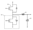
第2実施形態では、上記のように、上面電極層27の部分27aおよび27bを、互いに電気的に接続することによって、スイッチングトランジスタのソース−ドレイン間にショットキーバリアダイオードが電気的に接続された回路を容易に得ることができる。この場合、半導体装置12をDC/DCコンバータを構成する部品の一部として用いることができる(図11参照)。なお、図11中の符号31および32は、それぞれ、コイルおよびコンデンサである。また、図11中の符号33は、MOSトランジスタである。
In the second embodiment, as described above, the Schottky barrier diode is electrically connected between the source and the drain of the switching transistor by electrically connecting the
なお、第2実施形態のその他の効果は、上記第1実施形態と同様である。 The remaining effects of the second embodiment are similar to those of the aforementioned first embodiment.
図12は、本発明の第2実施形態の変形例による半導体装置を示した断面斜視図である。図12を参照して、第2実施形態の変形例による半導体装置13では、n型エピタキシャル層2の隣接するトレンチ3間の各領域に、上面電極層27に対してオーミック接触する領域(高濃度領域2a)と、上面電極層27に対してショットキー接触する領域(低濃度領域)とがA方向に1つずつ交互に設けられている。すなわち、n型エピタキシャル層2の隣接するトレンチ3間の各領域において、n型エピタキシャル層2の高濃度領域2aがA方向に断続的に設けられていることになる。
FIG. 12 is a cross-sectional perspective view showing a semiconductor device according to a modification of the second embodiment of the present invention. Referring to FIG. 12, in the
なお、第2実施形態の変形例のその他の構成は、上記第2実施形態と同様である。 In addition, the other structure of the modification of 2nd Embodiment is the same as that of the said 2nd Embodiment.
(第3実施形態)
図13は、本発明の第3実施形態による半導体装置の構造を説明するための断面図である。次に、図13を参照して、第3実施形態による半導体装置の構造について説明する。
(Third embodiment)
FIG. 13 is a cross-sectional view for explaining the structure of the semiconductor device according to the third embodiment of the present invention. Next, with reference to FIG. 13, the structure of the semiconductor device according to the third embodiment will be explained.
この第3実施形態の半導体装置14では、図13に示すように、n型エピタキシャル層2に、所定の制御信号(オン/オフの切り替えを行うための信号)が印加される埋め込み電極5(5a)が埋め込まれたトレンチ3(3a)のみが設けられている。
In the
そして、第3実施形態では、上面電極層7と裏面電極層8との間に電圧が印加された場合、上面電極層7と裏面電極層8との間を流れる電流は、隣接するトレンチ3a間の各領域を通過することになる。すなわち、第3実施形態では、隣接するトレンチ3a間の各領域が電流通路49として機能することになる。
In the third embodiment, when a voltage is applied between the
なお、第3実施形態のその他の構造は、上記した第1および第2実施形態のうちのいずれかの構造と同様である。 The remaining structure of the third embodiment is the same as that of any one of the first and second embodiments described above.
図14は、本発明の第3実施形態による半導体装置の動作を説明するための断面図である。次に、図13および図14を参照して、第3実施形態の半導体装置の動作について説明する。 FIG. 14 is a cross-sectional view for explaining the operation of the semiconductor device according to the third embodiment of the present invention. Next, with reference to FIGS. 13 and 14, the operation of the semiconductor device of the third embodiment will be described.
まず、オフ状態の場合には、図13に示すように、全てのトレンチ3aの周辺に空乏層10(10a)が形成されるように、全ての埋め込み電極5aに対して負電位が印加されている。これにより、電流通路49が空乏層10aによって塞がれた状態となるので、電流通路49を介して流れる電流を遮断することができる。
First, in the off state, as shown in FIG. 13, a negative potential is applied to all the embedded
そして、オフ状態からオン状態に切り替える場合には、図14に示すように、全ての埋め込み電極5aに対して正電位を印加することによって、図13に示した全ての空乏層10aを消滅させる。これにより、上面電極層7および裏面電極層8の各々に負電位および正電位が印加されているとすれば、電流通路49を介して図14中の矢印方向に電流を流すことができる。
When switching from the off state to the on state, as shown in FIG. 14, all the depletion layers 10a shown in FIG. 13 are extinguished by applying a positive potential to all the buried
この第3実施形態の効果は、上記第1実施形態の効果と同様である。 The effect of the third embodiment is the same as the effect of the first embodiment.
(第4実施形態)
図15は、本発明の第4実施形態による半導体装置の構造を説明するための断面図である。次に、図15を参照して、第4実施形態による半導体装置の構造について説明する。
(Fourth embodiment)
FIG. 15 is a cross-sectional view for explaining the structure of the semiconductor device according to the fourth embodiment of the present invention. Next, with reference to FIG. 15, the structure of the semiconductor device according to the fourth embodiment will be explained.
この第4実施形態の半導体装置15では、図15に示すように、n型エピタキシャル層2に、所定の制御信号が印加される埋め込み電極5(5a)が埋め込まれたトレンチ3(3a)と、上面電極層57のソース電極として機能する部分57aの一部(以下、埋め込み部57bと言う)が埋め込まれたトレンチ3(3d)とが設けられている。このトレンチ3aおよび3dは、互いに所定の間隔を隔てて1つずつ交互に配列されている。また、上面電極層57の埋め込み部57bは、トレンチ3dの内部において、エピタキシャル層2に対してショットキー接触している。なお、上面電極層57は、本発明の「電極層」の一例であり、部分57aは、本発明の「第2部分」の一例である。また、埋め込み部57bは、本発明の「埋め込み電極」および「第2埋め込み電極」の一例である。
In the
そして、第4実施形態では、上面電極層57と裏面電極層8との間に電圧が印加された場合、上面電極層57と裏面電極層8との間を流れる電流は、トレンチ3aとトレンチ3dとの間の各領域を通過することになる。すなわち、第4実施形態では、トレンチ3aとトレンチ3dとの間の各領域が電流通路59として機能することになる。
In the fourth embodiment, when a voltage is applied between the upper
なお、第4実施形態のその他の構造は、上記した第1および第2実施形態のうちのいずれかの構造と同様である。 The remaining structure of the fourth embodiment is the same as that of any one of the first and second embodiments described above.
図16は、本発明の第4実施形態による半導体装置の動作を説明するための断面図である。次に、図15および図16を参照して、第4実施形態による半導体装置の動作について説明する。 FIG. 16 is a cross-sectional view for explaining the operation of the semiconductor device according to the fourth embodiment of the present invention. Next, with reference to FIGS. 15 and 16, the operation of the semiconductor device according to the fourth embodiment will be described.
なお、以下の動作説明では、上面電極層57および裏面電極層8の各々に負電位および正電位が印加されているとする。すなわち、上面電極層57の埋め込み部57bが埋め込まれたトレンチ3dの周辺には、オン状態およびオフ状態にかかわらず、空乏層10(10d)が形成されている。
In the following description of the operation, it is assumed that a negative potential and a positive potential are applied to each of the
まず、オフ状態の場合には、図15に示すように、トレンチ3aの周辺に空乏層10(10a)が形成されるように、埋め込み電極5aに対して負電位が印加されている。これにより、電流通路59が空乏層10aおよび10dによって塞がれた状態となるので、電流通路59を介して流れる電流を遮断することができる。
First, in the off state, as shown in FIG. 15, a negative potential is applied to the buried
そして、オフ状態からオン状態に切り替える場合には、図16に示すように、埋め込み電極5aに対して正電位を印加することによって、図15に示した空乏層10aを消滅させる。これにより、電流通路59の埋め込み電極5a側の部分を介して図16中の矢印方向に電流を流すことができる。
When switching from the off state to the on state, as shown in FIG. 16, the
この第4実施形態の効果は、上記第1実施形態の効果と同様である。 The effect of the fourth embodiment is the same as the effect of the first embodiment.
(第5実施形態)
図17は、本発明の第5実施形態による半導体装置の構造を説明するための断面図である。次に、図17を参照して、第5実施形態による半導体装置の構造について説明する。
(Fifth embodiment)
FIG. 17 is a cross-sectional view for explaining the structure of the semiconductor device according to the fifth embodiment of the present invention. Next, with reference to FIG. 17, the structure of the semiconductor device according to the fifth embodiment will be explained.
この第5実施形態の半導体装置16では、図17に示すように、n型エピタキシャル層2に、所定の制御信号が印加される埋め込み電極5(5a)が埋め込まれたトレンチ3(3a)に加えて、p型不純物が高濃度で導入されたp+型拡散層61がさらに設けられている。このp+型拡散層61は、隣接するトレンチ3a間の各領域に、トレンチ3aに対して所定の間隔を隔てて1つずつ配置されている。また、p+型拡散層61は、上面電極層7に対してオーミック接触している。なお、p+型拡散層61は、本発明の「逆導電型の拡散層」の一例である。
In the
そして、第5実施形態では、上面電極層7と裏面電極層8との間に電圧が印加された場合、上面電極層7と裏面電極層8との間を流れる電流は、トレンチ3aとp+型拡散層61との間の各領域を通過することになる。すなわち、第5実施形態では、トレンチ3aとp+型拡散層61との間の各領域が電流通路69として機能することになる。
In the fifth embodiment, when a voltage is applied between the
なお、第5実施形態のその他の構造は、上記した第1および第2実施形態のうちのいずれかの構造と同様である。 The remaining structure of the fifth embodiment is the same as that of any one of the first and second embodiments described above.
図18は、本発明の第5実施形態による半導体装置の動作を説明するための断面図である。次に、図17および図18を参照して、第5実施形態による半導体装置の動作について説明する。 FIG. 18 is a cross-sectional view for explaining the operation of the semiconductor device according to the fifth embodiment of the present invention. Next, with reference to FIGS. 17 and 18, the operation of the semiconductor device according to the fifth embodiment will be explained.
なお、以下の動作説明では、上面電極層7および裏面電極層8の各々に負電位および正電位が印加されているとする。すなわち、p+型拡散層61の周辺には、オン状態およびオフ状態にかかわらず、空乏層10(10e)が形成されている。
In the following description of the operation, it is assumed that a negative potential and a positive potential are applied to each of the
まず、オフ状態の場合には、図17に示すように、トレンチ3aの周辺に空乏層10(10a)が形成されるように、埋め込み電極5aに対して負電位が印加されている。これにより、電流通路69が空乏層10aおよび10eによって塞がれた状態となるので、電流通路69を介して流れる電流を遮断することができる。
First, in the off state, as shown in FIG. 17, a negative potential is applied to the buried
そして、オフ状態からオン状態に切り替える場合には、図18に示すように、埋め込み電極5aに対して正電位を印加することによって、図17に示した空乏層10aを消滅させる。これにより、電流通路69の埋め込み電極5a側の部分を介して図18中の矢印方向に電流を流すことができる。
When switching from the off state to the on state, as shown in FIG. 18, the
この第5実施形態の効果は、上記第1実施形態の効果と同様である。 The effect of the fifth embodiment is the same as the effect of the first embodiment.
なお、今回開示された実施形態は、すべての点で例示であって制限的なものではないと考えられるべきである。本発明の範囲は、上記した実施形態の説明ではなく特許請求の範囲によって示され、さらに特許請求の範囲と均等の意味および範囲内でのすべての変更が含まれる。 The embodiment disclosed this time should be considered as illustrative in all points and not restrictive. The scope of the present invention is shown not by the above description of the embodiments but by the scope of claims for patent, and further includes all modifications within the meaning and scope equivalent to the scope of claims for patent.
たとえば、上記実施形態では、複数のトレンチをn型エピタキシャル層に形成し、そのn型エピタキシャル層の隣接するトレンチ間の各領域を電流通路として機能させるようにしたが、本発明はこれに限らず、複数のトレンチをp型エピタキシャル層に形成し、そのp型エピタキシャル層の隣接するトレンチ間の各領域を電流通路として機能させるようにしてもよい。 For example, in the above embodiment, a plurality of trenches are formed in the n-type epitaxial layer, and each region between adjacent trenches of the n-type epitaxial layer functions as a current path. However, the present invention is not limited to this. A plurality of trenches may be formed in the p-type epitaxial layer, and each region between adjacent trenches of the p-type epitaxial layer may function as a current path.
また、上記実施形態では、層間絶縁膜の上面がn型エピタキシャル層の上面に対して面一となるように構成したが、本発明はこれに限らず、層間絶縁膜の上面がn型エピタキシャル層の上面よりも上方に位置していてもよいし、層間絶縁膜の上面がn型エピタキシャル層の上面よりも下方に位置していてもよい。 In the above embodiment, the upper surface of the interlayer insulating film is flush with the upper surface of the n-type epitaxial layer. However, the present invention is not limited to this, and the upper surface of the interlayer insulating film is the n-type epitaxial layer. The upper surface of the interlayer insulating film may be positioned lower than the upper surface of the n-type epitaxial layer.
1 n+型シリコン基板(半導体層)
2 n型エピタキシャル層(半導体層)
3、3a、3b、3c、3d トレンチ
5、5c 埋め込み電極
5a 埋め込み電極(第1埋め込み電極)
5b 埋め込み電極(第2埋め込み電極)
7、27、57 上面電極層(電極層)
7a、27a、57a 部分(第2部分)
7b、27b 部分(第1部分)
9、49、59、69 電流通路
10、10a、10b、10c、10d、10e 空乏層
11、12、13、14、15、16 半導体装置
57b 埋め込み部(埋め込み電極、第2埋め込み電極)
61 p+型拡散層(拡散層)
1 n + type silicon substrate (semiconductor layer)
2 n-type epitaxial layer (semiconductor layer)
3, 3a, 3b, 3c,
5b Embedded electrode (second embedded electrode)
7, 27, 57 Upper surface electrode layer (electrode layer)
7a, 27a, 57a part (second part)
7b, 27b part (first part)
9, 49, 59, 69
61 p + type diffusion layer (diffusion layer)
Claims (10)
前記複数のトレンチの各々に埋め込まれた複数の埋め込み電極と、
前記半導体層の上面上に形成された電極層とを備え、
前記半導体層の隣接する前記トレンチ間の各領域が電流通路となり、かつ、前記トレンチの周辺に形成される空乏層で前記半導体層の前記隣接するトレンチ間の各領域が塞がれることにより前記電流通路が遮断される一方、前記トレンチの周辺に形成された空乏層の少なくとも一部が消滅することにより前記電流通路が開くように構成されており、
前記半導体層の前記隣接するトレンチ間の各領域のうちの所定領域の上面は、前記電極層に対してショットキー接触していることを特徴とする半導体装置。 A semiconductor layer of one conductivity type having a plurality of trenches arranged at predetermined intervals from each other and each opening end being located on the upper surface side;
A plurality of embedded electrodes embedded in each of the plurality of trenches;
An electrode layer formed on the upper surface of the semiconductor layer,
Each region between the adjacent trenches of the semiconductor layer serves as a current path, and each region between the adjacent trenches of the semiconductor layer is blocked by a depletion layer formed around the trench. While the passage is blocked, the current passage is configured to be opened when at least part of the depletion layer formed around the trench disappears,
The semiconductor device according to claim 1, wherein an upper surface of a predetermined region of each region between the adjacent trenches of the semiconductor layer is in Schottky contact with the electrode layer.
前記複数のトレンチのうちの全てのトレンチの周辺に形成される空乏層で前記隣接するトレンチ間の各領域が塞がれることにより前記電流通路が遮断される一方、前記複数のトレンチのうちの前記第1埋め込み電極が埋め込まれたトレンチの周辺に形成された空乏層が消滅することにより前記電流通路が開くように構成されていることを特徴とする請求項1〜6のいずれかに記載の半導体装置。 The plurality of embedded electrodes are divided into two types, a first embedded electrode and a second embedded electrode to which a voltage is applied separately from each other,
The current path is blocked by blocking each region between the adjacent trenches with a depletion layer formed around all of the plurality of trenches, while the one of the plurality of trenches is 7. The semiconductor according to claim 1, wherein the current path is opened when a depletion layer formed around a trench in which the first embedded electrode is embedded disappears. apparatus.
前記トレンチおよび前記拡散層の各々の周辺に形成される空乏層で前記隣接するトレンチ間の各領域が塞がれることにより前記電流通路が遮断される一方、前記トレンチの周辺に形成された空乏層が消滅することにより前記電流通路が開くように構成されていることを特徴とする請求項1〜6のいずれかに記載の半導体装置。 A diffusion layer of a reverse conductivity type formed in each region between the adjacent trenches of the semiconductor layer and disposed at a predetermined interval with respect to the trench;
A depletion layer formed around each of the trench and the diffusion layer blocks the current path by blocking each region between the adjacent trenches, while a depletion layer formed around the trench. 7. The semiconductor device according to claim 1, wherein the current path is opened when the current disappears.
Priority Applications (2)
| Application Number | Priority Date | Filing Date | Title |
|---|---|---|---|
| JP2007176582A JP5285242B2 (en) | 2007-07-04 | 2007-07-04 | Semiconductor device |
| PCT/JP2008/062104 WO2009005131A1 (en) | 2007-07-04 | 2008-07-03 | Semiconductor device |
Applications Claiming Priority (1)
| Application Number | Priority Date | Filing Date | Title |
|---|---|---|---|
| JP2007176582A JP5285242B2 (en) | 2007-07-04 | 2007-07-04 | Semiconductor device |
Publications (2)
| Publication Number | Publication Date |
|---|---|
| JP2009016571A true JP2009016571A (en) | 2009-01-22 |
| JP5285242B2 JP5285242B2 (en) | 2013-09-11 |
Family
ID=40226172
Family Applications (1)
| Application Number | Title | Priority Date | Filing Date |
|---|---|---|---|
| JP2007176582A Active JP5285242B2 (en) | 2007-07-04 | 2007-07-04 | Semiconductor device |
Country Status (2)
| Country | Link |
|---|---|
| JP (1) | JP5285242B2 (en) |
| WO (1) | WO2009005131A1 (en) |
Cited By (1)
| Publication number | Priority date | Publication date | Assignee | Title |
|---|---|---|---|---|
| JP7114824B1 (en) * | 2021-09-17 | 2022-08-08 | ヌヴォトンテクノロジージャパン株式会社 | semiconductor equipment |
Citations (9)
| Publication number | Priority date | Publication date | Assignee | Title |
|---|---|---|---|---|
| JPH0215677A (en) * | 1988-04-27 | 1990-01-19 | General Electric Co (Ge) | Single conductivity type umos field effect semiconductor device |
| JPH03289141A (en) * | 1990-04-06 | 1991-12-19 | Nissan Motor Co Ltd | Manufacture of semiconductor device |
| JPH0846192A (en) * | 1994-08-01 | 1996-02-16 | Nissan Motor Co Ltd | Semiconductor device |
| JP2001168333A (en) * | 1999-09-30 | 2001-06-22 | Toshiba Corp | Semiconductor device equipped with trench gate |
| JP2004134547A (en) * | 2002-10-10 | 2004-04-30 | Hitachi Ltd | Semiconductor device |
| JP2005286059A (en) * | 2004-03-29 | 2005-10-13 | Sanyo Electric Co Ltd | Semiconductor device |
| US20060011962A1 (en) * | 2003-12-30 | 2006-01-19 | Kocon Christopher B | Accumulation device with charge balance structure and method of forming the same |
| JP2007134469A (en) * | 2005-06-22 | 2007-05-31 | Sanyo Electric Co Ltd | Insulated-gate semiconductor device and manufacturing method thereof |
| JP2007529115A (en) * | 2003-12-30 | 2007-10-18 | フェアチャイルド・セミコンダクター・コーポレーション | Power semiconductor device and manufacturing method thereof |
Family Cites Families (1)
| Publication number | Priority date | Publication date | Assignee | Title |
|---|---|---|---|---|
| US6593620B1 (en) * | 2000-10-06 | 2003-07-15 | General Semiconductor, Inc. | Trench DMOS transistor with embedded trench schottky rectifier |
-
2007
- 2007-07-04 JP JP2007176582A patent/JP5285242B2/en active Active
-
2008
- 2008-07-03 WO PCT/JP2008/062104 patent/WO2009005131A1/en active Application Filing
Patent Citations (9)
| Publication number | Priority date | Publication date | Assignee | Title |
|---|---|---|---|---|
| JPH0215677A (en) * | 1988-04-27 | 1990-01-19 | General Electric Co (Ge) | Single conductivity type umos field effect semiconductor device |
| JPH03289141A (en) * | 1990-04-06 | 1991-12-19 | Nissan Motor Co Ltd | Manufacture of semiconductor device |
| JPH0846192A (en) * | 1994-08-01 | 1996-02-16 | Nissan Motor Co Ltd | Semiconductor device |
| JP2001168333A (en) * | 1999-09-30 | 2001-06-22 | Toshiba Corp | Semiconductor device equipped with trench gate |
| JP2004134547A (en) * | 2002-10-10 | 2004-04-30 | Hitachi Ltd | Semiconductor device |
| US20060011962A1 (en) * | 2003-12-30 | 2006-01-19 | Kocon Christopher B | Accumulation device with charge balance structure and method of forming the same |
| JP2007529115A (en) * | 2003-12-30 | 2007-10-18 | フェアチャイルド・セミコンダクター・コーポレーション | Power semiconductor device and manufacturing method thereof |
| JP2005286059A (en) * | 2004-03-29 | 2005-10-13 | Sanyo Electric Co Ltd | Semiconductor device |
| JP2007134469A (en) * | 2005-06-22 | 2007-05-31 | Sanyo Electric Co Ltd | Insulated-gate semiconductor device and manufacturing method thereof |
Cited By (3)
| Publication number | Priority date | Publication date | Assignee | Title |
|---|---|---|---|---|
| JP7114824B1 (en) * | 2021-09-17 | 2022-08-08 | ヌヴォトンテクノロジージャパン株式会社 | semiconductor equipment |
| WO2023042359A1 (en) * | 2021-09-17 | 2023-03-23 | ヌヴォトンテクノロジージャパン株式会社 | Semiconductor device |
| US11637176B2 (en) | 2021-09-17 | 2023-04-25 | Nuvoton Technology Corporation Japan | Semiconductor device |
Also Published As
| Publication number | Publication date |
|---|---|
| JP5285242B2 (en) | 2013-09-11 |
| WO2009005131A1 (en) | 2009-01-08 |
Similar Documents
| Publication | Publication Date | Title |
|---|---|---|
| US8217419B2 (en) | Semiconductor device | |
| JP2010109221A (en) | Semiconductor device | |
| JP2009004411A (en) | Semiconductor device | |
| JP2005259766A (en) | Semiconductor device | |
| US20110204439A1 (en) | Semiconductor device | |
| JP2006295062A (en) | Semiconductor device | |
| US10269945B2 (en) | Power transistor device | |
| JP5285242B2 (en) | Semiconductor device | |
| JP2009004501A (en) | Semiconductor device | |
| JP5207666B2 (en) | Semiconductor device | |
| US10319851B2 (en) | Semiconductor device and method for manufacturing same | |
| US8575687B2 (en) | Semiconductor switch device | |
| US8860129B2 (en) | Semiconductor device | |
| JP2008300494A (en) | Semiconductor device | |
| TWI517414B (en) | Schokkty diode with enhanced breakdown voltage | |
| JP2008311453A (en) | Semiconductor device | |
| JP6555284B2 (en) | Semiconductor device | |
| JP2008300495A (en) | Semiconductor device | |
| JP2008300496A (en) | Semiconductor device | |
| JP2009004399A (en) | Semiconductor device | |
| JP3376294B2 (en) | Semiconductor device | |
| JP5389339B2 (en) | Semiconductor device | |
| US10475792B2 (en) | Power transistor device | |
| JP2008305904A (en) | Semiconductor device | |
| JP5230970B2 (en) | Semiconductor device |
Legal Events
| Date | Code | Title | Description |
|---|---|---|---|
| A621 | Written request for application examination |
Free format text: JAPANESE INTERMEDIATE CODE: A621 Effective date: 20100607 |
|
| A131 | Notification of reasons for refusal |
Free format text: JAPANESE INTERMEDIATE CODE: A131 Effective date: 20120820 |
|
| A521 | Request for written amendment filed |
Free format text: JAPANESE INTERMEDIATE CODE: A523 Effective date: 20121019 |
|
| A131 | Notification of reasons for refusal |
Free format text: JAPANESE INTERMEDIATE CODE: A131 Effective date: 20121113 |
|
| A521 | Request for written amendment filed |
Free format text: JAPANESE INTERMEDIATE CODE: A523 Effective date: 20130108 |
|
| A131 | Notification of reasons for refusal |
Free format text: JAPANESE INTERMEDIATE CODE: A131 Effective date: 20130129 |
|
| A521 | Request for written amendment filed |
Free format text: JAPANESE INTERMEDIATE CODE: A523 Effective date: 20130326 |
|
| TRDD | Decision of grant or rejection written | ||
| A01 | Written decision to grant a patent or to grant a registration (utility model) |
Free format text: JAPANESE INTERMEDIATE CODE: A01 Effective date: 20130507 |
|
| A61 | First payment of annual fees (during grant procedure) |
Free format text: JAPANESE INTERMEDIATE CODE: A61 Effective date: 20130531 |
|
| R150 | Certificate of patent or registration of utility model |
Ref document number: 5285242 Country of ref document: JP Free format text: JAPANESE INTERMEDIATE CODE: R150 |
|
| R250 | Receipt of annual fees |
Free format text: JAPANESE INTERMEDIATE CODE: R250 |
|
| RD03 | Notification of appointment of power of attorney |
Free format text: JAPANESE INTERMEDIATE CODE: R3D03 |
|
| R250 | Receipt of annual fees |
Free format text: JAPANESE INTERMEDIATE CODE: R250 |
|
| R250 | Receipt of annual fees |
Free format text: JAPANESE INTERMEDIATE CODE: R250 |
|
| R250 | Receipt of annual fees |
Free format text: JAPANESE INTERMEDIATE CODE: R250 |
|
| R250 | Receipt of annual fees |
Free format text: JAPANESE INTERMEDIATE CODE: R250 |