JP2008544283A - Method and apparatus for adjusting a multi-substrate probe structure - Google Patents
Method and apparatus for adjusting a multi-substrate probe structure Download PDFInfo
- Publication number
- JP2008544283A JP2008544283A JP2008518368A JP2008518368A JP2008544283A JP 2008544283 A JP2008544283 A JP 2008544283A JP 2008518368 A JP2008518368 A JP 2008518368A JP 2008518368 A JP2008518368 A JP 2008518368A JP 2008544283 A JP2008544283 A JP 2008544283A
- Authority
- JP
- Japan
- Prior art keywords
- probe
- card assembly
- probe card
- assembly
- mounting structure
- Prior art date
- Legal status (The legal status is an assumption and is not a legal conclusion. Google has not performed a legal analysis and makes no representation as to the accuracy of the status listed.)
- Pending
Links
Images


Classifications
-
- G—PHYSICS
- G01—MEASURING; TESTING
- G01R—MEASURING ELECTRIC VARIABLES; MEASURING MAGNETIC VARIABLES
- G01R31/00—Arrangements for testing electric properties; Arrangements for locating electric faults; Arrangements for electrical testing characterised by what is being tested not provided for elsewhere
- G01R31/28—Testing of electronic circuits, e.g. by signal tracer
- G01R31/2851—Testing of integrated circuits [IC]
- G01R31/2886—Features relating to contacting the IC under test, e.g. probe heads; chucks
-
- G—PHYSICS
- G01—MEASURING; TESTING
- G01R—MEASURING ELECTRIC VARIABLES; MEASURING MAGNETIC VARIABLES
- G01R31/00—Arrangements for testing electric properties; Arrangements for locating electric faults; Arrangements for electrical testing characterised by what is being tested not provided for elsewhere
- G01R31/28—Testing of electronic circuits, e.g. by signal tracer
- G01R31/317—Testing of digital circuits
- G01R31/3181—Functional testing
- G01R31/319—Tester hardware, i.e. output processing circuits
- G01R31/31903—Tester hardware, i.e. output processing circuits tester configuration
- G01R31/31905—Interface with the device under test [DUT], e.g. arrangements between the test head and the DUT, mechanical aspects, fixture
-
- H—ELECTRICITY
- H01—ELECTRIC ELEMENTS
- H01L—SEMICONDUCTOR DEVICES NOT COVERED BY CLASS H10
- H01L22/00—Testing or measuring during manufacture or treatment; Reliability measurements, i.e. testing of parts without further processing to modify the parts as such; Structural arrangements therefor
-
- G—PHYSICS
- G01—MEASURING; TESTING
- G01R—MEASURING ELECTRIC VARIABLES; MEASURING MAGNETIC VARIABLES
- G01R1/00—Details of instruments or arrangements of the types included in groups G01R5/00 - G01R13/00 and G01R31/00
- G01R1/02—General constructional details
- G01R1/06—Measuring leads; Measuring probes
- G01R1/067—Measuring probes
- G01R1/073—Multiple probes
-
- Y—GENERAL TAGGING OF NEW TECHNOLOGICAL DEVELOPMENTS; GENERAL TAGGING OF CROSS-SECTIONAL TECHNOLOGIES SPANNING OVER SEVERAL SECTIONS OF THE IPC; TECHNICAL SUBJECTS COVERED BY FORMER USPC CROSS-REFERENCE ART COLLECTIONS [XRACs] AND DIGESTS
- Y10—TECHNICAL SUBJECTS COVERED BY FORMER USPC
- Y10T—TECHNICAL SUBJECTS COVERED BY FORMER US CLASSIFICATION
- Y10T29/00—Metal working
- Y10T29/49—Method of mechanical manufacture
- Y10T29/49002—Electrical device making
- Y10T29/49117—Conductor or circuit manufacturing
- Y10T29/49124—On flat or curved insulated base, e.g., printed circuit, etc.
- Y10T29/49128—Assembling formed circuit to base
-
- Y—GENERAL TAGGING OF NEW TECHNOLOGICAL DEVELOPMENTS; GENERAL TAGGING OF CROSS-SECTIONAL TECHNOLOGIES SPANNING OVER SEVERAL SECTIONS OF THE IPC; TECHNICAL SUBJECTS COVERED BY FORMER USPC CROSS-REFERENCE ART COLLECTIONS [XRACs] AND DIGESTS
- Y10—TECHNICAL SUBJECTS COVERED BY FORMER USPC
- Y10T—TECHNICAL SUBJECTS COVERED BY FORMER US CLASSIFICATION
- Y10T29/00—Metal working
- Y10T29/49—Method of mechanical manufacture
- Y10T29/49002—Electrical device making
- Y10T29/49117—Conductor or circuit manufacturing
- Y10T29/49124—On flat or curved insulated base, e.g., printed circuit, etc.
- Y10T29/4913—Assembling to base an electrical component, e.g., capacitor, etc.
- Y10T29/49133—Assembling to base an electrical component, e.g., capacitor, etc. with component orienting
-
- Y—GENERAL TAGGING OF NEW TECHNOLOGICAL DEVELOPMENTS; GENERAL TAGGING OF CROSS-SECTIONAL TECHNOLOGIES SPANNING OVER SEVERAL SECTIONS OF THE IPC; TECHNICAL SUBJECTS COVERED BY FORMER USPC CROSS-REFERENCE ART COLLECTIONS [XRACs] AND DIGESTS
- Y10—TECHNICAL SUBJECTS COVERED BY FORMER USPC
- Y10T—TECHNICAL SUBJECTS COVERED BY FORMER US CLASSIFICATION
- Y10T29/00—Metal working
- Y10T29/49—Method of mechanical manufacture
- Y10T29/49002—Electrical device making
- Y10T29/49117—Conductor or circuit manufacturing
- Y10T29/49124—On flat or curved insulated base, e.g., printed circuit, etc.
- Y10T29/49147—Assembling terminal to base
-
- Y—GENERAL TAGGING OF NEW TECHNOLOGICAL DEVELOPMENTS; GENERAL TAGGING OF CROSS-SECTIONAL TECHNOLOGIES SPANNING OVER SEVERAL SECTIONS OF THE IPC; TECHNICAL SUBJECTS COVERED BY FORMER USPC CROSS-REFERENCE ART COLLECTIONS [XRACs] AND DIGESTS
- Y10—TECHNICAL SUBJECTS COVERED BY FORMER USPC
- Y10T—TECHNICAL SUBJECTS COVERED BY FORMER US CLASSIFICATION
- Y10T29/00—Metal working
- Y10T29/49—Method of mechanical manufacture
- Y10T29/49002—Electrical device making
- Y10T29/49117—Conductor or circuit manufacturing
- Y10T29/49204—Contact or terminal manufacturing
- Y10T29/49208—Contact or terminal manufacturing by assembling plural parts
- Y10T29/49222—Contact or terminal manufacturing by assembling plural parts forming array of contacts or terminals
Landscapes
- Engineering & Computer Science (AREA)
- General Engineering & Computer Science (AREA)
- Physics & Mathematics (AREA)
- General Physics & Mathematics (AREA)
- Computer Hardware Design (AREA)
- Microelectronics & Electronic Packaging (AREA)
- Manufacturing & Machinery (AREA)
- Power Engineering (AREA)
- Testing Or Measuring Of Semiconductors Or The Like (AREA)
- Measuring Leads Or Probes (AREA)
- Tests Of Electronic Circuits (AREA)
Abstract
プローブカードアセンブリは、実装アセンブリに取り付けられたマルチのプローブ基板を備える。各プローブ基板は、1セットのプローブを備える。各プローブ基板上のこれらのプローブセットは一緒に検査すべきデバイスに接触するプローブアレイを構成する。調節機構は、各プローブ基板に力を加えて実装アセンブリに対して各基板を個々に移動させるように構成される。これらの調節機構は、各プローブ基板を「x」、「y」および/または「z」方向に平行移動させることができ、また、さらに、各プローブ基板を前記方向のうちの任意の1つまたは複数の方向の周りに回転させることができる。さらに、これらの調節機構は、1つまたは複数のプローブ基板の形状を変えることができる。したがって、これらのプローブは、検査すべきデバイス上の接点に対してアライメントしかつ/または面一になることができる。 The probe card assembly includes multiple probe substrates attached to the mounting assembly. Each probe board includes a set of probes. These probe sets on each probe substrate together constitute a probe array that contacts the device to be tested. The adjustment mechanism is configured to apply a force to each probe substrate to individually move each substrate relative to the mounting assembly. These adjustment mechanisms can translate each probe substrate in the “x”, “y” and / or “z” directions, and further each probe substrate in any one of the directions or Can be rotated around multiple directions. Further, these adjustment mechanisms can change the shape of one or more probe substrates. Thus, these probes can be aligned and / or flush with the contacts on the device to be tested.
Description
図1は、電子デバイス検査用の例示的な検査システム90を示す。この電子デバイスは、たとえば、新たに製造された半導体ウエハ12上のダイ(図示せず)でよい。図1の検査システム90は、テストヘッド4とプローバ2(プローバ2の内部の部分図を与える切り取り部26で示される)とを備える。この半導体ウエハ12のダイ(図示せず)を検査するために、このウエハ12は図1に示す可動ステージ6上に載置され、このステージ6はウエハ12のダイ(図示せず)上の端子22がプローブカードアセンブリ20のプローブ66と接触するように移動される。このようにして、一時的な電気接続がプローブ66と検査すべきウエハ12のダイ(図示せず)との間に生じる。
FIG. 1 illustrates an exemplary inspection system 90 for electronic device inspection. This electronic device may be, for example, a die (not shown) on a newly manufactured
一般的に、ケーブル10または他の通信手段はテスタ(図示せず)にテストヘッド4を接続する。電気コネクタ14は、テストヘッド4にプローブカードアセンブリ20を電気接続し、このプローブカードアセンブリ20は、プローブ66への電気経路(図示せず)を備える。したがって、ケーブル10、テストヘッド4、電気コネクタ14、およびプローブカードアセンブリ20(プローブ66を含む)は、テスタ(図示せず)と検査されるウエハ12のダイ端子22との間に電気経路を与える。すなわち、プローブ66がウエハ12上のダイ(図示せず)の端子22と接触している間は、ケーブル10、テストヘッド4、電気コネクタ14、およびプローブカードアセンブリ20は、テスタ(図示せず)とダイ(図示せず)との間に複数の電気経路を提供する。このテスタ(図示せず)によってテストデータが電気経路を介してこれらのダイ(図示せず)に書き込まれ、このテストデータに応答してこれらのダイにより生成された応答データがこれらの電気経路を介してテスタに戻される。
Generally, a
典型的なウエハ12は多数のダイ(図示せず)を含む。実際、ウエハ12は数十または数百ものダイ(図示せず)を含んでよい。一般的に、プローブカードアセンブリ20は、ウエハ12上のダイ(図示せず)の全てには接触できない。ウエハ12上の全てのダイ(図示せず)を検査するために、ステージ6によりウエハ12のダイ(図示せず)のいくつかを移動させてプローブカードアセンブリ20のプローブ66に接触させ、テスタ(図示せず)でこれらのダイ(図示せず)につき検査を行う。次いで、このステージ6により他のダイ(図示せず)をプローブ66に接触させるようにウエハ12を移動し、テスタ(図示せず)でこれらのダイにつき同じ検査を行う。ウエハ12の全てのダイ(図示せず)が検査されるまで、このウエハ12の移動過程により、いくつかのダイ(図示せず)をプローブ66に接触させて、これらのダイ(図示せず)の検査を行う。
A
プローブカードアセンブリ技術が進歩するに伴って、より多くのダイ(図示せず)に接触するためにプローブ66のアレイの寸法が大きくなってきた。大きなプローブアレイ66を作製する1つの方法は、多数のプローブ基板66を用いることを伴う。すなわち、それぞれが複数のプローブを備える多数のプローブ基板66が、プローブ基板66上のプローブが大きなプローブアレイを形成するように互いに隣接して配置される。米国特許第5,806,181号、第6,690,185号、第6,640,415号、および第6,509,751号(これらの各々はその全体が参照により本明細書に組み込まれている)には、多数のプローブ基板を有するプローブカードアセンブリの非限定的な例が開示されている。これらのプローブ66とダイ端子22とは、一般的に小さく、正確に整列されなければならない。これによって、多数のプローブ基板の正確な位置決めが必要とされる。このようなプローブ基板を正確に位置決めする方法および装置が必要とされる。
As probe card assembly technology has advanced, the size of the array of probes 66 has increased to contact more dies (not shown). One method of making a large probe array 66 involves using multiple probe substrates 66. That is, a large number of probe substrates 66 each having a plurality of probes are arranged adjacent to each other such that the probes on the probe substrate 66 form a large probe array. US Pat. Nos. 5,806,181, 6,690,185, 6,640,415, and 6,509,751, each of which is incorporated herein by reference in its entirety. Discloses a non-limiting example of a probe card assembly having multiple probe substrates. These probes 66 and die
例示的な実施形態では、多数のプローブ基板が実装アセンブリに接着される。各プローブ基板にはそれぞれ1セットのプローブが備えられ、プローブ基板上のこれらのプローブセットは一緒に検査すべきデバイスに接触するためのプローブのアレイを構成する。調節機構が、各プローブ基板に力を加えて各基板を実装アセンブリに対して個々に移動させるように構成される。この調節機構は、「x」、「y」および/または「z」軸に沿って各プローブ基板を平行移動させることができ、さらに各プローブ基板を1つまたは複数の前記軸の周りに回転させることができる。さらに、この調節機構は1つまたは複数のプローブ基板の形状を変えることができる。したがって、これらのプローブは、検査されるデバイス上の接点に対して整列しかつ/または平坦になることができる。 In the exemplary embodiment, multiple probe substrates are bonded to the mounting assembly. Each probe substrate is provided with a set of probes, and these probe sets on the probe substrate together constitute an array of probes for contacting the device to be tested. An adjustment mechanism is configured to apply a force to each probe substrate to move each substrate individually relative to the mounting assembly. This adjustment mechanism can translate each probe substrate along the “x”, “y” and / or “z” axes, and further rotate each probe substrate about one or more of said axes. be able to. In addition, the adjustment mechanism can change the shape of one or more probe substrates. Thus, these probes can be aligned and / or flat with respect to the contacts on the device being tested.
この明細書は、本発明の例示的な実施形態および用途につき説明する。しかし、本発明はこれらの例示的な実施形態および用途、あるいはこれらの例示的な実施形態および用途が本明細書中で機能しまたは説明される方法に限定されない。 This specification describes exemplary embodiments and applications of the invention. However, the present invention is not limited to these exemplary embodiments and applications, or the methods by which these exemplary embodiments and applications function or are described herein.
図2Aおよび図3に、複数のプローブ基板108を備える例示的なプローブカードアセンブリ100の簡略化したブロック図を示す。(図2Aにプローブカードアセンブリ100の側面図を示し、図3にプローブカードアセンブリ100の下面図を示す。)1セットのプローブ112が各プローブ基板108に取り付けられ、これらのプローブ基板108はこれらのプローブセット112がプローブの大きなアレイを形成するように配列される。4つのプローブ基板108が示されているが、より少ないプローブ基板またはより多くのプローブ基板を用いてもよい。このプローブカードアセンブリ100を、プローブカードアセンブリ20の代わりに図1のシステム90のような検査システムに用いてもよい。そして、議論を簡単にするために、本明細書では、このプローブカードアセンブリ100を検査システム90に関して論じる。
2A and 3 show simplified block diagrams of an exemplary
図2Aおよび図3に示されるように、プローブカードアセンブリ100は、コネクタ102、実装アセンブリ104、およびそれぞれが1セットのプローブ112を有するプローブ基板108を備える。接続機構114は、このプローブ基板108を物理的に実装アセンブリ104に接続する。第1の調節機構106および第2の調節機構110は実装アセンブリ104に対するプローブ基板108の位置を調節するように構成される。図2Aおよび図3での描写は必ずしも比例していない。たとえば、プローブ基板108の間隔はより接近してよいが、図2Aおよび図3では図示を簡単にするために描写している。
As shown in FIGS. 2A and 3, the
コネクタ102はテストヘッド4(図1参照)と電気接続するように構成される。たとえば、コネクタ102は、ZIF(zero insertion force)コネクタまたはポゴピンコネクタを受け入れるポゴパッドを含むがこれらに限定されない任意のタイプの電気コネクタでよい。
The
図2Bはプローブカードアセンブリ100の概略図を示し、そこでは実装アセンブリ104を通る電気経路152(たとえば、導電性の線および/またはビア)、実装アセンブリ104とプローブ基板108との間の電気接続154(たとえば、ワイヤ、インターポーザなど)、およびプローブ基板108を通る電気経路156(たとえば、導電配線および/またはビア)が、プローブセット112とコネクタ102を電気接続する。
FIG. 2B shows a schematic diagram of the
電気経路152の付与に加えて、この実装アセンブリ104は、図1のシステム90のような検査システムのプローバ2に確実に取り付けるように構成される。たとえば、この実装アセンブリ104は、プローバ2にボルト(図示せず)止めしてもよく、クランプ(図示せず)締めしてもよく、または他の方法で固定してもよい。
In addition to providing an
例示的な実装アセンブリ104の簡略化したブロック図を示す図2Cに示されるように、この実装アセンブリ104にはスティフナプレート182と配線基板184とを含んでよい。配線基板184は、実装アセンブリ104を通るコネクタ102(図2Cに図示せず)からの電気経路152を与える。この配線基板184は、たとえば、プリント回路板でよい。スティフナプレート182は、そりおよび熱誘導された移動等に耐える機械的剛性を与える。配線基板184をプローバ2(図1参照)に固定してよい。また、スティフナプレート182を配線基板184に取り付けて配線基板184を補強してもよい。米国特許第5,974,662号の例が図5に示され、そこではプリント回路板502が配線基板184の例であり、実装プレート530および532がスティフナプレート182の例である。あるいは、スティフナプレート184をプローバ2に固定してもよく、配線基板184をこのスティフナプレート182に取り付けてもよい。「プローブカードアセンブリ中の熱的に誘導される動きに対処するための装置および方法」という名称の米国特許仮出願第60/594,562号(2005年4月19日出願)に例が示されている。たとえば、米国特許仮出願第60/594,562号における図面全体にわたって示されるスティフナプレート202はスティフナプレート182の例である。そして、やはり米国特許仮出願第60/594,562号における図面全体にわたって示される配線基板204は配線基板184の例である。前述の米国特許第5,974,662号および米国特許仮出願第60/594,562号は本明細書にそれらの全体が参照により組み込まれている。
As shown in FIG. 2C, which shows a simplified block diagram of an
取付け機構114は、総称的に図2Aで箱として表され、上記したようにプローブ基板108を実装アセンブリ104に物理的に接続するように構成される。好ましくは、この取付け機構110は、プローブ基板108を実装アセンブリ104のスティフナプレート182部に物理的に接続する。さらに、取付け機構114はプローブ基板108を特定の方向に付勢するように構成してもよい。図3に示される例では、このプローブ基板108は矢印116の方向に付勢される。これによって図3に示すように各プローブ基板108を他のプローブ基板から遠ざけて付勢する。付勢配置の代替例としては、1つのプローブ基板108がどの方向にも付勢されないが、基準として働き、他のプローブ基板108のそれぞれがそれから遠ざかって付勢される。たとえば、代わりに、図3の下側右隅に位置するプローブ基板108がどの方向にも付勢されず、他の3つのプローブ基板108のそれぞれが他のプローブ基板から矢印116の方向に遠ざかって付勢される。
The
各プローブ基板108は、プローブセット112用のプラットフォームを含み、このプローブ基板108を通ってプローブ112に至る電気経路156(図2B参照)を備える。たとえば、プローブ基板108は、電気経路156を形成する導電配線(図示せず)および導電ビア(図示せず)を有するセラミック基板または有機基板を含んでよい。
Each
プローブ112は弾性的で導電性の構造物でよい。適切なプローブ112の非限定的な例には、プローブ基板108上の導電性端子(図示せず)に接合されたコアワイヤで形成された複合構造物が含まれる。このプローブ基板108は、米国特許第5,476,211号、第5,917,707号、および第6,336,269号に記載された弾性材料で被覆され、これらの特許はその全体が本明細書に参照により組み込まれている。代わりに、これらのプローブ112は、米国特許第5,994,152号、第6,033,935号および第6,255,126号、ならびに米国特許出願第2001/0044225号および第2001/0012739号に開示されたばね要素などのリソグラフィで形成された構造物でよい。これらの特許のそれぞれも、その全体が本明細書に参照により組み込まれている。プローブ112の他の非限定的な例には、導電性ポゴピン、バンプ、スタッド、打ち抜きばね等が含まれる。
The
第1の調節機構106および第2の調節機構110によって、各プローブ基板108の位置を実装アセンブリ104に対して変更できる。実装アセンブリ104はプローバ2に確実に取り付けられているので、各プローブ基板108の位置も、ステージ6(図1参照)上に配設されたプローバ2および検査すべきウエハ12(図1参照)に対して変更される。したがって、プローブ112を、ダイ端子22に整列させ、かつ/またはダイ端子22に面一にすることができる。
The position of each
好ましくは、これらの第1の調節機構106と第2の調節機構110は、各プローブ基板108を6段階に移動させるように構成される。図2Aでは、これらの6段階の移動を以下のように名付ける。すなわち、図2Aのページを横切る水平方向を「x」、図2Aのページに入りかつ紙面から出る水平方向を「y」、垂直方向を「z」、「x」軸周りの回転をRx、「y」軸周りの回転をRy、および「z」軸周りの回転をRzと名付ける。上記の方向は議論を容易にするために与えられたものであって限定するものではない。
Preferably, the
第1の調節機構106はプローブ基板108の1つまたは複数の部分を「z」方向に移動させるように構成される。したがって、この第1の調節機構106は各プローブ基板108を3段階の動作(すなわち、「z」軸に沿った平行移動、「x」軸の周りの回転Rx、および「y」軸の周りの回転Ry)で移動させることができる。第2の調節機構110は「x−y」平面内でプローブ基板108の1つまたは複数の部分を移動させるように構成される。したがって、この第2の調節機構110は各プローブ基板108を追加の3段階の動作(すなわち、「x」軸に沿った平行移動、「y」軸に沿った平行移動、および「z」軸の周りの回転Rz)で移動させることができる。
The
図4〜図8には、例示的なプローブカードアセンブリ400が示されている。これらの図中、図2Aおよび図3の取付け機構114のそれぞれがフレーム410とばねアセンブリ408とを含み、第1の調節機構106のそれぞれが差動ねじ404を含み、また、第2の調節機構110のそれぞれがカムアセンブリ406を含む。図示したように、このプローブカードアセンブリ400も、図2Aおよび図3におけるように、コネクタ102と実装アセンブリ104とプローブ基板108とプローブ112とを含む。(図示を容易にするために図4〜図8の描写は必ずしも比例していない。たとえば、プローブ基板108の間隔はより近接してよいが、図4〜図8では図示を容易にするために描写している。)
An exemplary
上記したように、図2Aおよび3の取付け機構114は、プローブカードアセンブリ400ではフレーム410およびばねアセンブリ408として実装されている。図4および図6に示すように、複数のばねアセンブリ408がフレーム410を実装アセンブリ104に取り付ける。図9に、オープンスペース802を備える例示的なフレーム410の透視図を示す。プローブ基板108はフレーム410に取り付けられ、この取付けをボルト、クランプ、接着剤、粘着剤等で実現してよい。プローブカードアセンブリ400の側面断面図を示す図8に示すように、インターポーザ804がフレーム410の各空間802内に嵌合される。図8にやはり示すように、好ましくは、各インターポーザ804は、実装アセンブリ104と接触するための第1のセットの導電性ばね要素808と、プローブ基板108と接触するための第2のセットの導電性ばね要素810とを含む。これらの第1の組のばね接触要素808は、インターポーザ基板806を通って第2の組のばね接触要素810まで電気接続される。したがって、各インターポーザ804は、実装アセンブリ104とプローブ基板108との間に電気経路154を与える(図2B参照)。そして、接触要素808および810がばねであるのでこれらの電気経路154はコンプライアント(従順)である(すなわち、これらの電気経路154は、実装アセンブリ104に対するプローブ基板108の位置がカムアセンブリ406および差動ねじアセンブリ404によって変えられても保たれたままである)。上記で論じたように、接触要素808および810は、プローブ112のように構築してよい。前記米国特許第5,974,662号の図5でのインターポーザ504と前記米国特許第6,509,751号(その全体が本明細書に参照により組み込まれている)の図2Aでのインターポーザ230とは、適切なインターポーザ804の非限定的な例である。各フレーム410内のスペース802には、プローブ基板108あたり4つのインターポーザ804が与えられるが、より少ないまたはより多いインターポーザ804をプローブ基板108あたりに用いてもよい。
As described above, the
図6(プローブカードアセンブリ400の下面図を示す)に示すように、各フレーム(図6でプローブ基板108の後ろに隠れている)は複数のばねアセンブリ408により実装アセンブリ104に取り付けられる。図10Aおよび図10Bに、このようなばねアセンブリ408の1つの詳細な側面図および正面図をそれぞれ示す。図10Aおよび図10Bに示すように、このばねアセンブリ408は実装アセンブリ104に取り付けられたピン1002とフレーム410に取り付けられたピン1006とを備える。(実装アセンブリ104、フレーム410、およびプローブ基板108は、図10Aおよび図10Bに部分図で示される。)フレームピン1006は、フレーム410と一体的に形成してよく、または、フレームピン1006をフレーム410中の穴(図示せず)内にねじ込むか詰め込んでもよい。同様に、アセンブリピン1002を実装アセンブリ104と一体的に形成してよく、またはアセンブリピン1002を実装アセンブリ104中の穴(図示せず)内にねじ込むか詰め込んでもよい。代わりに、ピン1002およびピン1006を、実装アセンブリ104およびフレーム410に、のり付け、溶接、接着、ろう付け、はんだ付けまたは他の方法で、それぞれ取り付けてもよい。
As shown in FIG. 6 (showing a bottom view of the probe card assembly 400), each frame (hidden behind the
ばね1004はアセンブリピン1002とフレームピン1006の両方に取り付けられる。このばね1004は、任意の適切なばね構造物でよく、任意の適切な方法でアセンブリピン1002とフレームピン1006とに取り付けてよい(たとえば、ばね1004の端部をピン1002および1006中の穴(図示せず)に固定してよく、ばね1004の端部をピン1002および1006等の周りに巻いてもよい)。
The
このばねアセンブリ408は、フレーム410を実装アセンブリ104に取り付けるだけでなく、プローブ基板108の付勢もする。図10Aを参照すると、ばねアセンブリ408は、図10Aの矢印1010により示されるようにプローブ基板108(フレーム410に取り付けられた)を上方かつページ内に付勢する。図10Aの側面図を示す図10Bでは、付勢方向は、矢印1010により示されるように上方および左である。ばねアセンブリ408を選択的に載置することによってブローブ基板108を任意の所望の方向に付勢することができる。たとえば、図6(プローブカードアセンブリ400の下面図を示す)に示すようにプローブカードアセンブリ400上にばねアセンブリ408を載置することによって、図6に示した4つのプローブ基板108を互いに遠ざけて(図3での矢印116方向と同様に)実装アセンブリ104に向けて付勢する。
This
上記および図7に示すように、図2Aおよび図3の第1の調節機構106は、図4〜図8のプローブカードアセンブリ400では複数の差動ねじアセンブリ404および対応するピボット球体1106として実装される。図11Aに、このような差動ねじアセンブリ404の1つと対応するピボット球体1106との詳細な断面図を示す。(図11Aに、実装アセンブリ104とフレーム410とプローブ基板とを部分図で示す。)図示されているように、この差動ねじアセンブリ404は、実装アセンブリ104に動けないように堅く移動不可能に固定された外側のねじ込み要素1104を備える。ねじ1102がこの外側要素1104内にねじ込まれる。図11Bに示すように、ねじ1102が一方向に回転(108)すると、ピボット球体1106に向かって下方に移動する。このピボット球体1106はフレーム410中の窪み902内に配設され、それによって、このフレーム410(そしてプローブ基板108も)を実装アセンブリ104から遠ざけて押す。ねじ1102を反対方向(図示せず)に回転させると、ねじ1102はピボット球体1106から遠ざかって引込み、ばねアセンブリ408(上記したように、フレーム410を実装アセンブリ104の方に付勢する)のばね作用によりフレーム410がねじ1102によって移動する。
As described above and shown in FIG. 7, the
図9に示すように、フレーム410は9つのピボット球体1106(図9に示さず)用の9つの窪み902を有し、したがって、9つの差動ねじアセンブリ404によって移動するように構成されている。(プローブカードアセンブリ400の側面断面図を示す図7に、3つのこのような差動ねじアセンブリ404を示す。これらの差動ねじアセンブリ404は、図7に示した2つのフレーム410用のものである。)図14に示すように、9つの差動ねじアセンブリ404によって9つの力1406がもたらされてフレーム410(図14にブロック図形態で示す)に向けられる。そして、これらの9つの力1406のそれぞれを選択的に用いることによってこのフレーム410(そしてこのフレームに取り付けられたプローブ基板108(図14に示さず)は「z」軸に沿って平行移動し、「x」軸と「y」軸の両軸の周りを回転(Rx、Ry)することができる。しかしもちろん、9つより少ないかまたはそれより多くの差動ねじアセンブリ404を用いて1つのプローブ基板108を調節してもよい。
As shown in FIG. 9, the
上記したように、図2Aおよび図3の第2の調節機構110は、図4〜図8のプローブカードアセンブリ400で複数のカムアセンブリ406として実装される。図12Aはこのようなカムアセンブリ406の1つの側面図であり、図13Aはその下面図である。図示したように、カム1204はねじ1202に堅く取り付けられ、このねじはポスト1206中のねじ穴(図示せず)内にねじ込まれる。このポスト1206は実装アセンブリ104に堅く取り付けられる。ねじ1202の回転によってカム1204が回転する。図12Bおよび図13Bに示すように、カム1204はフレーム410に当接し、カム1204が一方向に回転(1308)すると、このカム1204はフレーム410を押し移動(1210)させる。カム1204が反対方向(図示せず)に回転すると、このカム1204はフレーム410から遠ざかって移動し、また、ばねアセンブリ408のばね作用(上記で論じたようにフレーム410を付勢する)によってフレーム410がカム1204で押される。
As described above, the
図4および6に示されるように、8つのカムアセンブリ406が、各フレーム410(図6では、フレーム410は各プローブ基板108の下に隠れている)の周りに位置する。図14に示すように、8つのカムアセンブリ408によって8つの力1404がもたらされてフレーム410(図14でブロック図の形態で示した)に向けられる。これら8つの力1404のそれぞれを選択的に用いることによって、フレーム410(そしてフレームに取り付けられたプローブ基板108)が「x」および「y」軸に沿って平行移動し、「z」軸の周りに回転(Rz)することができる。しかしもちろん、8つより少ないかまたはそれより多くのカムアセンブリ406を用いて1つのプローブ基板108を調節してよい。たとえば、カムアセンブリ406は、プローブ基板108の全ての側面に沿って位置する必要はない。たとえば、カムアセンブリ408は、これらのカムアセンブリ408がばねアセンブリ408の付勢方向に対抗しているプローブ基板108の側面上のみに位置してよい。
As shown in FIGS. 4 and 6, eight
図15〜図17に、別の例示的なプローブカードアセンブリ1500を示す。図15にプローブカードアセンブリ1500の下面図、図16にその上面図、図17にその側面断面図を、それぞれ示す。図示を簡単にするために、図15〜図17での描写は必ずしも比例していない。たとえば、プローブ基板108の間隔はより近接してよいが、図15〜図17では図示を容易にするために描写している。プローブカードアセンブリ1500は、いくつかの点でプローブカードアセンブリ400に類似している。
FIGS. 15-17 illustrate another exemplary
プローブカードアセンブリ400のように、プローブカードアセンブリ1500は検査システムに使用してよい。たとえば、プローブカードアセンブリ1500は、図1の検査システム90でのプローブカードアセンブリ20の代わりに用いてもよい。さらに、プローブカードアセンブリ1500はコネクタ102および実装アセンブリ104を含む。これらは、プローブカードアセンブリ400で同様に呼ばれ番号が付与された要素と同じでよい。また、プローブカードアセンブリ400のように、プローブカードアセンブリ1500は複数のプローブ基板108(4つが図示されているが、これより少ないかまたは多くの基板を用いてもよい)を含み、これらの基板は、各プローブ基板108上のプローブセット112が一緒に大きなプローブアレイを形成するように配列される。
Like
しかし、プローブカードアセンブリ1500では、図2Aおよび図3の取付け機構114はレベリングねじアセンブリ1504によって実装されている。図2Aおよび図3の第1の調節機構106もレベリングねじアセンブリ1504によって実装されており、また図2Aおよび図3の第2の調節機構110はこのレベリングねじアセンブリ1504とブラケット1510中の位置決めねじ1506とによって実装される。図15〜図17に示す例示的なばねアセンブリ1508は、圧縮状態にある。したがって、図15に示す各ばねアセンブリ1508は、ばねアセンブリ1508が取り付けられた2つのプローブ基板108を互いに遠ざけて付勢する。ばねアセンブリ1508は、一般的にプローブカードアセンブリ400でのばねアセンブリ408に構造が類似しているが、フレーム410と実装アセンブリ104との間ではなくプローブ基板108間に取り付けられる。
However, in the
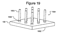
特に図17に示すように、プローブ基板108は、レベリングねじアセンブリ1504によって実装アセンブリ104に取り付けられ、これらレベリングねじアセンブリ1504のそれぞれは実装アセンブリ104中の通路1702を通って延びる。図17中左端のレベリングねじアセンブリ1504の詳細図を示した図18Aに示すように、各レベリングねじアセンブリ1504は、ねじ1802とロックナット1804とねじ付き溶接スタッド1806とを備える。このねじ付き溶接スタッド1806はプローブ基板108に取り付けられる。このねじ付き溶接スタッド1806をプローブ基板108に取り付ける方法は、重要ではない。そして、限定されることなく以下の方法、すなわち、溶接、ろう付け、のり付け、接着等のうちの任意の方法を用いてもよい。レベリングねじアセンブリ1504は、プローブ基板108を実装アセンブリ104に取り付ける。すなわち、このレベリングねじアセンブリ1504は図2Aの取付け機構114の別の例である。
In particular, as shown in FIG. 17, the
図18Aに示すように、ねじ1802の軸1803がスタッド1806中のねじ穴(図示せず)内にねじ込まれる。図18Bに示すように、ねじ1802が一方向に回転(1858)すると、このねじ1802は後退し、スタッド1806にそしてプローブ基板108にも引張り力を及ぼす。この引張り力はプローブ基板108を実装アセンブリ104の方に移動(1860)させる。ねじ1802が反対方向に回転(1858)すると、このねじ1802は前進し、スタッド1806そしてプローブ基板108にも押し込み力を及ぼす。この押し込み力はプローブ基板108を実装アセンブリ104から遠ざけて移動(1860)させる。したがって、レベリングねじアセンブリ1504は、それらが取り付けられているプローブ基板108を垂直(図18A〜図18Dと相対的に)に移動させる。すなわち、このレベリングねじ1504も、図2A中の第1の調節機構106の別の例である。
As shown in FIG. 18A, the
図18Cに示すように、実装アセンブリ104中の通路1702は十分に大きく、ねじ1802を通路1702内を横方向に移動(1850)させることができる。ロックナット1804が非係合位置(図18Cに示さず)にある間は、レベリングねじアセンブリ1504は横方向(図18Aから図18Dに相対的に)に移動(1850)することができ、また、図18Cに示すように、ねじ付き溶接スタッド1806が取り付けられたプローブ基板108も移動させる。好ましくは、通路1702は、横方向移動1850がプローブ基板108の平面内のどんな方向(たとえば、図2Aに示した「x−y」平面)への移動も含むように構成される。ロックナット1804が係合位置(図18Aに示す)にある間は、レベリングねじアセンブリ1504は所定位置にロックされ、通路1702内で横方向に移動(1850)できない。
As shown in FIG. 18C, the
図18Dに示すように、位置決めねじ1506はブラケット1510中のねじ穴(図示せず)を通ってねじ込まれる。このブラケットは、任意の適切な手段(たとえば、ボルト、ねじ、クランプ、のり、接着剤等)を用いて実装アセンブリに取り付けられる。位置決めねじ1854の一方向への回転1854によって、位置決めねじ1854はプローブ基板108の方に前進し、それによって、プローブ基板が横方向に押される1856。位置決めねじ1854の反対方向への回転1854によって、位置決めねじ1854はプローブ基板108から遠ざかって引込む。ばね1508(図18Dに示さず)の付勢効果の故に、プローブ基板108は、位置決めねじが引込むと、位置決めねじ1506によって移動される。(上記で論じたように、例示的なばね1508は好ましくは圧縮状態にあり、それ故、図15および図17に示すように構成される。このばね1508は、位置決めねじ1506によりプローブ基板108に加えられる力と反対の力をプローブ基板108に加える。)ねじ1802の軸1803は、好ましくは、図18Dに示すように湾曲し、ロックナット1804がロックされている間はプローブ基板108が移動可能である。これによって、上記で論じたように、レベリングねじアセンブリ1504が通路1702内で横方向移動するのを防ぐ。代わりに、レベリングねじアセンブリ1504内のねじ1802の軸1803は、この軸1803が位置決めねじ1506によりプローブ基板108上に加えられる力と反対の対抗力をプローブ基板108に与えるように弾性的(すなわち、ばね状)であってもよい。このような弾性的な軸1803は、プローブカードアセンブリ1500の初期の組立て時に、プローブ基板108を互いに遠ざけて付勢するように構成してもよい。軸1803が弾性的であると、ばね1508を用いる必要がない。さらに別の代替形態として、ばね1506と弾性的な軸1803との両方を用いてもよい。
As shown in FIG. 18D, the
上記で論じたように、レベリングねじアセンブリ1504と位置決めねじ1506との両方は、プローブ基板108の横方向移動1856(図18Dに関連して)をもたらすことができる。好ましい実施形態では、レベリングねじアセンブリ1504の通路1702内の移動はプローブ基板108の横方向の粗調整用であり、位置決めねじ1506はプローブ基板108の横方向の微調整用に用いる。したがって、レベリングねじアセンブリ1504と位置決めねじ1506とは、図2Aの第2の調節機構110の別の例である。
As discussed above, both leveling
図19に示すように、例示的なプローブ基板108のそれぞれは9つのねじ付き溶接スタッド1806を有し、これら9つのねじ付き溶接スタッド内にはレベリングねじアセンブリ1504のねじ1802の9つの軸1803(図19中の部分図に示す)がねじ込まれている。(しかしもちろん、9つより少ないかまたはそれより多くのレベリングねじアセンブリ1504を用いて1つのプローブ基板108を調節してもよい。)図20に示すように、9つのレベリングねじアセンブリ1504によって9つの力2006がもたらされてプローブ基板108に向けられる。そして、これらの9つの力2006のそれぞれを選択的に用いることによってこのプローブ基板108は「z」軸に沿って平行移動し、「x」軸と「y」軸の両軸の周りを回転(Rx、Ry)することができる。図21に示すように、レベリングねじアセンブリ1504がプローブ基板108に押付け力または引張り力を与えることができるので、このレベリングねじアセンブリ1504はプローブ基板108の形状をさらに変化させ、それによって、プローブ基板108の湾曲または屈曲などを矯正することができる。図20の側面図を示す図21では、交互の押付け力および引張り力がプローブ基板108に加えられ、それによって、プローブ(図21に示さず)が取り付けられているプローブ基板108の表面1902の形状が変えられる。図21でこの表面1902の形状が変更される程度は、図示するために誇張されている。一般的に、この表面1902は、ほんの僅か変更されて表面1902またはダイ端子22(図1参照)の平坦度の軽微な欠陥が補償される。前記した米国特許第6,509,751号には、プローブ基板の形状が変更される例が開示され、論じられている。
As shown in FIG. 19, each of the
図15に最適に見られるように、4つの位置決めねじ1506がプローブカードアセンブリ1500中の各プローブ基板108の周りに位置決めされる。図20に示すように、この4つの位置決めねじ1506によって4つの力2004がもたらされてプローブ基板108に向けられる。そして、これらの4つの力2004のそれぞれを選択的に用いること(および図18Cに示すようにレベリングねじアセンブリ1504を選択的に横方向移動させること)によってこのプローブ基板108は「x」軸と「y」軸に沿って平行移動し、「z」軸の周りを回転(Rz)することができる。しかしもちろん、4つより少ないかまたはそれより多くの位置決めねじ1506を用いて1つのプローブ基板108を調節してもよい。
As best seen in FIG. 15, four set
図17を再度参照すると、ワイヤ1704が実装アセンブリ104とプローブ基板108の間に電気経路154(図2B参照)を付与している。各ワイヤ1704は、その一端で実装アセンブリ104上の導電端子(図示せず)に取り付け(たとえば、はんだ付け)、他端でプローブ基板108上の導電端子(図示せず)に取り付け(たとえば、はんだ付け)てよい。このワイヤ1704は可撓性を有してプローブ基板108の移動に対応してもよい。
Referring again to FIG. 17, the
図22Aに、例示的な横方向調節アセンブリ2202を示す。この横方向調節アセンブリ2202は、プローブカードアセンブリ400のカムアセンブリ406またはプローブカードアセンブリ1500の位置決めねじ1506の代わりに用いてもよい。図示したように、このアセンブリ2202は、ねじ込みねじ2204を含む差動ねじ構造体を備え、このねじ込みねじ2204の軸2208は、実装アセンブリ104に埋め込まれ、取り付けられ、一体形成され、または他の方法で固定された外側要素2206内にねじ穴(図示せず)を通ってねじ込まれる。この軸2208は、隣接するプローブ基板108上に配設された受け入れ構造体2212間に配設された球体2210を押す。ばね2214は、プローブ基板を一緒に引っ張る傾向のある力を与える(たとえば、ばね2214は伸びた状態にある)。
FIG. 22A illustrates an exemplary
図22Bに示すように、ねじ2204が一方向に回転(2250)すると、軸2208は前進し、その結果、球体2210をプローブ基板108の方に押し、プローブ基板108を横方向に遠ざける(2252)。ねじ2204が反対方向に回転(2250)すると、軸2208が球体2210から遠ざかって引込み、ばね2214がプローブ基板108を互いに向かって引っ張る。
As shown in FIG. 22B, when the
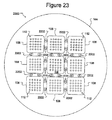
図22Aに示した横方向調節アセンブリ2202は、それ故、図2Aおよび図3の第2の調節機構110の別の例である。図22Aの横方向調節アセンブリ2202は、プローブ基板108のうちの少なくとも1つが他のプローブ基板108により囲まれているプローブカードアセンブリで特に役立つことができる。このようなプローブカードアセンブリ2300の例を図23(プローブカードアセンブリ2300の下面図を示す)に示す。図示したようにこのプローブカードアセンブリ2300は9つのプローブ基板108を備え、そのそれぞれがプローブセット112を有する。中央のプローブ基板は他のプローブ基板108により囲まれているので、その調節機構(ねじ2204)が実装アセンブリ104の他の側からアクセス可能な調節アセンブリ2202を使用すれば、その調節機構がプローブ基板(たとえば、プローブカードアセンブリ1500の位置決めねじ1506)の側方に位置するアセンブリよりも使い易くできる。(図示を簡単にするために、図23の描写は必ずしも比例していない。たとえば、プローブ基板108の間隔はより接近してよいが、図23では図示を簡単にするために描写している。)
The
図24〜図26には、さらに別の例示的なプローブカードアセンブリ2400を示す。図24にプローブカードアセンブリ2400の側面図、図25にその上面図、図26にその下面図を示す。図示を簡単にするために、図24〜図26の描写は必ずしも比例していない。)
24-26 illustrate yet another exemplary
プローブカードアセンブリ2400は、いくつかの点でプローブカードアセンブリ1500に類似している。プローブカードアセンブリ1500のように、プローブカードアセンブリ2400は検査システムに使用してよい。たとえば、プローブカードアセンブリ2400は、図1の検査システム90でのプローブカードアセンブリ20の代わりに用いてもよい。さらに、プローブカードアセンブリ2400はコネクタ(図示しないが、プローブカードアセンブリ1500のコネクタ102と類似している)および実装アセンブリ104を含む。この実装アセンブリは、プローブカードアセンブリ1500の実装アセンブリ104と同じでよい。図24に示すように、実装アセンブリ104は、好ましくは、図2Cに関して図示し論じたようにスティフナプレート182と配線基板184とを備える。また、プローブカードアセンブリ1500のように、プローブカードアセンブリ2400は複数のプローブ基板108(4つが図示されているが、これより少ないかまたは多くの基板を用いてもよい)を含み、これらの基板は、各プローブ基板108上のプローブセット112が一緒に大きなプローブアレイを形成するように配列される。図4〜図6のプローブカードアセンブリ400のように、プローブカードアセンブリ2400はインターポーザ804(それぞれが、図8に示すように、ばね接触要素806および810とインターポーザ基板806とを備える)を備える。このインターポーザ804は、図8に関して上記したように、配線基板184とプローブ基板108との間に可撓性かつ/または弾性的電気接続を付与するためのものである。代わりに、インターポーザ804は、図17に示される可撓性ワイヤ1704などの他の可撓性電気接続で置き換えてもよい。
しかし、プローブカードアセンブリ2400では、図2Aおよび図3中の取付け機構114と第1の調節機構106と第2の調節機構110とは、アライメントプレート2402とアライメント/平坦化(「AP」)アセンブリ2408とによって実装される。図示したように、プローブカードアセンブリ2400には、各プローブ基板108につき1つのアライメントプレート2402があり、各アライメントプレート2402毎に9つのAPアセンブリ2408がある。しかしもちろん、プローブ基板108あたりより少ないかまたはそれより多くのアライメントプレート2402を用いてよく、また、アライメントプレート2402あたりより少ないかまたはそれより多くのAPアセンブリ2408を用いてもよい。
However, in the
図27〜図29に、これら4つのアライメントプレート2402のうちの1つの詳細な説明図を示す。図25の部分図である図27に1つのアライメントプレート2402の上面図を示し、図28および図29に図27のアライメントプレート2402の側面断面図を示す。プローブカードアセンブリ2400のアライメントプレート2402の4つ全てを同様に構成してよい。
27 to 29 show detailed explanatory diagrams of one of these four
アライメントプレート2402は、メタル基板でよく、各APアセンブリ2408にアクセスするための開口2714とツール通路2710とを備える。(4つのツール通路2710を示すが、これより少ない通路またはこれより多くの通路を用いてよい。)図示するように図27では、9つのAPアセンブリ2408がアライメントプレート2402に取り付けられる。(上記のごとく、9つより少ないAPアセンブリ2408またはそれより多くのAPアセンブリ2408を用いてよい。)
The
図29に最適に見られるように、各APアセンブリ2408はハウジング2712と差動ねじアセンブリ2708とを備え、この差動ねじアセンブリ2708はプローブ基板108に取り付けられたスタッド2806内にねじ込まれるスタッドエクステンダ2804を備える。差動ねじアセンブリ2708は、好ましくは分割ナット構成である。差動ねじアセンブリ2708は、一般的に、プローブカードアセンブリ1500のレベリングねじアセンブリ1504のように働くことができる。すなわち、この差動ねじアセンブリ2708は、レベリングねじアセンブリ1504のように、ねじ付き溶接スタッド2806に押付け力または引張り力を及ぼすことができる。図18Bの示す移動と同様に、差動ねじアセンブリ2708の一方向への回転によってスタッド2806(そしてプローブ基板108)が実装アセンブリ104の方に引っ張られ、差動ねじアセンブリ2708の反対方向への回転によってスタッド2806(そしてプローブ基板108)が実装アセンブリ104から遠ざかって押される。10ミクロン以下のオーダでの微調整を提供する分割ナット差動ねじ、およびこのような精密な分割ナット差動ねじを用いてよい。ツール(図示せず)が開口2714を介して差動ねじアセンブリ2708に係合してもよい。
As best seen in FIG. 29, each
また、図29に最適に示すように、ハウジング2712は、実装アセンブリ104のアライメントプレート2402とスティフナプレート182との間に位置する。(このハウジング2712はアライメントプレート2402の後ろに位置し、したがって図27では視界の外になる。しかし、図示を容易にするために、このハウジング2712を図27に含めたが、点線で示した。)ハウジング2712は、取付けねじ2704によってアライメントプレート2402に移動不可能に取り付けられる。しかし、ブレーキねじ2702(図27中でのみ見ることができる)によって、ハウジング2712がスティフナプレート182に対して移動可能かどうかが決定される。ブレーキねじ2702が緩められている間は、ハウジング2712はスティフナプレート182に対して横方向移動できる(図29および図30に関して)。各APアセンブリ2408の差動ねじ2708(そのスタッドエクステンダ2806を含む)は、スタッド2806と共にハウジング2712によって移動2952する。スティフナプレート182中の通路2904と配線基板184中の通路2906とによって、スタッドエクステンダ2804はスティフナプレート182および配線板184に対して移動することができる。しかし、ブレーキねじ2702が締付けられている間は、ハウジング2712そして全APアセンブリ2408が所定の位置にロックされスティフナプレート182に対して移動できない。したがって、ブレーキねじ2702は、プローブアセンブリ1500の差動ねじアセンブリ1504のロックナット1804のように働き、図18Cに示す移動1850のような横方向移動を可能にする。
Also, as best shown in FIG. 29, the
図28に示すように、2つ以上のレバレッジツール2860(たとえば、ねじ回し)をアライメントプレート2402中のツール通路2710を通って、スティフナプレート182の開口2802内に挿入してよい。次いで、これらのレバレッジツール2860をてことして用いてアライメントプレート2402に横方向(図28および図29に関して)の力を加えてもよい。APアセンブリ2408のハウジング2712が取付けねじ2704によってアライメントプレート2402に堅く取り付けられるので、これらの力はアライメントプレート2402をスティフナプレート182に対して移動(2852)させるだけでなく、ハウジング2712のそれぞれも移動させる。これによって、APアセンブリ2408のスタッド2806が取り付けられたプローブ基板108を次々に移動(2854)させる。もちろん、これらのハウジング2712とプローブ基板108は、各ハウジング2712のブレーキねじ2702が緩められたときのみ移動する。これらのブレーキねじ2702が締付けられているときは、これらのハウジング2712は移動しない。
As shown in FIG. 28, two or more leverage tools 2860 (eg, screwdrivers) may be inserted through the
したがって、アライメントプレート2402およびAPアセンブリ2408は、プローブカードアセンブリ2400中の各プローブ基板108の平坦度および/またはアライメントを6段階の異なる移動で調節し、プローブ基板108の形状を変更することができる。すなわち、図30に示すように、アライメントプレート2402を通る2対のツール通路2710およびスティフナプレート182(図28参照)中の穴2802内に挿入された2つのレバレッジツール2860は、「x−y」平面中のどの方向にも横方向の力3004を与えることができる。そして、これらの力3004によって、プローブ基板108は、「x」軸および/または「y」軸に沿った平行移動ならびに/または「z」軸の周りの回転(Rz)をする。また、9つのAPアセンブリ2408がプローブ基板108に押付け力および/または引張り力を加えることができるので、これらの9つのAPアセンブリ2408は、図20に示したのと同じ9つの押付け力または引張り力2006をもたらしてプローブ基板108上に向けることができる。図20に示すように、これらの9つの力を選択的に用いることによって、このプローブ基板108を「z」軸に沿って平行移動し、「x」および「y」の両軸の周りに回転させる(Rx、Ry)ことができる。これらの6段階の移動−「x」、「y」および「z」軸に沿った平行移動、およびこれらの軸それぞれの周りの回転(Rx、Ry、Rz)−に加えて、図21に示すようにプローブ基板108に押付け力と引張り力を交互に加えることによって、このプローブ基板108の形状を変えることができる。
Accordingly, the
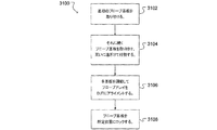
図31に、プローブカードアセンブリ(たとえば、100、400、1500、2300、2400)を製造する例示的な工程3100を示す。このプローブカードアセンブリでは、検査すべきデバイスに接触するためのプローブアレイが、別個のプローブ基板(たとえば、108)上にそれぞれ配設された複数のプローブセット(たとえば、112)から構成されている。
FIG. 31 illustrates an
ステップ3102では、第1の組のプローブ112を備えるプローブ基板108が実装アセンブリ104に取り付けられる。たとえば、図3に示した下側右のプローブ基板108を実装アセンブリ104に取り付けてもよい。ステップ3104では、追加のプローブ基板108が実装アセンブリ104に取り付けられる。たとえば、図3の上側右、上側左および下側左のプローブ基板108を実装アセンブリ104に取り付ける。ステップ3102およびステップ3104で実装アセンブリ104に取り付けられたプローブ基板108は、各プローブ基板108が本明細書で説明したように調節(たとえば、平坦化かつアライメント)できるように上記の任意の技法および任意の機構を用いて取り付けてよい。たとえば、各プローブ基板108は、プローブカードアセンブリ400のばねアセンブリ408、プローブカードアセンブリ1500のレベリングねじアセンブリ1504、またはプローブカードアセンブリ2400のAPアセンブリ2408を用いて実装アセンブリ104に取り付けてもよい。
In
ステップ3104で述べたように、各プローブ基板108が実装アセンブリ104に取り付けられると、プローブ基板108は他のプローブ基板108から遠ざかって付勢され得る。たとえば、ステップ3102で実装アセンブリ104に取り付けられた第1のプローブ基板108はどの方向にも付勢され得ず、ステップ3104でその後実装アセンブリに取り付けられたプローブ基板108は第1の基板から遠ざかって付勢され得る。あるいは、ステップ3102およびステップ3104で取り付けられた全てのプローブ基板108は互いに遠ざかって付勢され得る。さらに別の代替案としては、プローブ基板108を付勢する必要がない。1つまたは複数のプローブ基板108が付勢される場合、プローブカードアセンブリ400のばねアセンブリ408、プローブカードアセンブリ1500のばねアセンブリ1508、またはプローブカードアセンブリ2300のばね2214を用いて付勢してもよい。
As described in
ステップ3106では、ステップ3102およびステップ3104で取り付けられた1つまたは複数のプローブ基板108のアライメントおよび/または平坦度を調節してプローブアレイ(各プローブ基板108上のプローブセット112からなる)をアライメントかつ/または平坦化する。上記で論じたように、図2Aおよび図3の第1の調節機構106および第2の調節機構110を用いて1つまたは複数のプローブ基板108を「x」、「y」および/または「z」軸に沿って移動させ、かつ/または図2Aに示し上記で論じたようにこれらのプローブ基板108を「x」、「y」および/または「z」軸の周りに回転(Rx、Ry、Rz)させてもよい。たとえば、プローブカードアセンブリ400の差動ねじアセンブリ404とカムアセンブリ406を用いて、ステップ3102およびステップ3104で実装アセンブリ104に取り付けられた1つまたは複数のプローブ基板108に図14に示した力および移動を与えてもよい。別の例として、プローブカードアセンブリ1500のレベリングねじアセンブリ1504と位置決めねじ1506とを用いて1つまたは複数のプローブ基板108に図20に示した力および移動を与えてもよい。また、レベリングねじアセンブリ1504を用いて図21に示したように1つまたは複数のプローブ基板108の形状を変更してもよい。さらに別の例として、プローブカードアセンブリ2400のアライメントプレート2402とAPアセンブリ2408とを用いて1つまたは複数のプローブ基板108に図20および図30に示した力および移動を与えてもよい。また、APアセンブリ2408を用いて図21に示したように1つまたは複数のプローブ基板108の形状を変更してもよい。
In
ステップ3106の際にプローブ基板108に与えられる移動によって、インターポーザ804(図8参照)のばね接点808および810が、実装アセンブリ104上かつ/またはプローブ基板108上の接触端子(図示せず)を横切ってスクラビングすることができる。知られているように、端子を横切って接点をスクラビングさせることによって接点と端子との間の電気接続が向上する。これは、このスクラビング作用によって端子上の非伝導性(電気的に)すなわち電気抵抗の高い不純物(たとえば、酸化物)を突き抜けることができるからである。
The movement imparted to the
ステップ3108では、各プローブ基板(この段階では、ステップ3106によりダイ端子22にアライメントしかつ/または面一になった)の位置を所定位置にロックする。図示していないが、第1の調節機構106と第2の調節機構110とは、プローブ基板108を実装アセンブリ104に対して選択された位置にロックするように構成してよい。たとえば、プローブカードアセンブリ400の差動ねじアセンブリ404は、プローブカードアセンブリ400が回転(1108)できないようにねじ1102をロックする機構を備えてよい。カムアセンブリ406のねじ1202も同様なロック機構を備えてよい。あるいは、これらの差動ねじアセンブリ404およびカムアセンブリ406は、回転ツール(図示せず)をねじ1102および1202に用いない限りこれらのねじ1102および1202が回転に耐えるように構成してもよい。このような場合、ステップ3108は、ステップ3106が完了した直後に連累して実施される。レベリングねじアセンブリ1504のねじ1802、横方向調節アセンブリ2202のねじ2204、およびAPアセンブリ2408の差動ねじ2708は、同様にロック機構(図示せず)で構成して回転ツールを用いない限り回転に耐えるようにしてもよい。これらとは無関係に、レベリングねじアセンブリ1504のロックナット1804は、上記したように、レベリングねじアセンブリ1504が通路1702内を横方向に移動するのをロックし止める。同様に、プローブカードアセンブリ2400のAPアセンブリ2408のロックねじ2702は、APアセンブリ2408が通路2904および2906内を横方向に移動するのをロックし止める(図29参照)。このようなアセンブリを用いてステップ3106で横方向調節を行うときは、ステップ3108でロックナット1804およびロックねじ2702がロックされる。
In
上記で論じたように、プローブ基板108は、ステップ3106で実装アセンブリ104に対して調節される。実装アセンブリ104はプローバ(たとえば、図1のプローバ2のような)に取り付けてよく、検査すべきウエハ12はこのプローバ2内に配設してよいので、プローブ基板108(と取り付けられたプローブ112と)をプローバ2に対して調節することによって、プローブ基板(と取り付けられたプローブ112と)をプローバ2およびウエハ12のダイ端子22に対して調節する。このプローブ112が検査すべきウエハ12のダイ端子22に対して面一にかつ/または整列されるとすぐに、ステージ6がダイ端子22を移動してプローブ112に接触させることができ、ウエハ12のダイ端子を検査することができる。
As discussed above, the
本明細書で、本発明の具体的な実施形態および用途を説明してきたが、これらの例示的な実施形態および用途、またはこれらの例示的な実施形態および用途が本明細書で機能し説明される方法に本発明が限定されることは意図されていない。たとえば、カムアセンブリ406のねじ1202は、カムアセンブリ406が図12Aに示すようにプローブカードアセンブリ400の下面からではなくその上面から調節できるように、実装アセンブリ104の上面を通って延びてもよい。さらに別の例として、第1の調節機構106と第2の調節機構110(図2Aおよび図3参照)の様々な例を混合し調和させてもよい。一例として、プローブアセンブリ400のカムアセンブリ406を、プローブカードアセンブリ1500のブラケット1510と位置決めねじ1506とで置き換えてもよい。同様に、プローブカードアセンブリ1500のブラケット1500と位置決めねじ1506とをカムアセンブリ406で置き換えてもよい。さらに別の例として、プローブカードアセンブリ1500のレベリングねじアセンブリ1504のうちのいくつかを、プローブカードアセンブリ400の差動ねじアセンブリ404と置き換えてもよい。したがって、図20に示した力2006は押付け力のみでよい。本明細書で説明した実施形態の修正のさらに別の例として、プローブカードアセンブリ1500の可撓性ワイヤ1704を、プローブカードアセンブリ400にインターポーザ804に替えて用いてもよい。同様に、プローブカードアセンブリ400のインターポーザ804を、プローブカードアセンブリ1500に可撓性ワイヤ1704に替えて用いてもよい。さらに別の例として、第1の調節機構106および第2の調節機構110は、コンピュータまたは他の自動制御システムにより生成された制御信号に応答して自動作動装置によって駆動してもよい。本明細書で説明した実施形態の変更のさらに別の例として、これらの実施形態はプローブカードアセンブリであったが、本明細書で説明したアライメント技法および平坦化技法は、一般的に、平坦化かつ/またはアライメントしなければならない1つまたは複数の基板を備える任意のデバイスに用いるのに適している。
Although specific embodiments and applications of the present invention have been described herein, these exemplary embodiments and applications, or these exemplary embodiments and applications, function and are described herein. It is not intended that the present invention be limited to such methods. For example, the
Claims (34)
実装構造体と、
前記検査すべきデバイスに接触するように配置されたプローブセットを含むプローブ基板と、
前記プローブ基板を前記実装構造体に対して略平行に移動させるための第1の移動手段と、
を含む、プローブカードアセンブリ。 A probe card assembly for contacting a device to be inspected,
A mounting structure;
A probe substrate including a probe set arranged to contact the device to be inspected;
First moving means for moving the probe substrate substantially parallel to the mounting structure;
Including a probe card assembly.
複数のプローブ基板をさらに含み、各々の前記プローブ基板が、前記検査すべきデバイスに接触するように配置された追加のプローブセットを含み、前記第1の移動手段は2つ以上の前記プローブ基板を前記実装構造体に対して略平行に移動可能である、プローブカードアセンブリ。 The probe card assembly of claim 1,
A plurality of probe substrates, each probe substrate including an additional probe set arranged to contact the device to be inspected, wherein the first moving means includes two or more probe substrates; A probe card assembly that is movable substantially parallel to the mounting structure.
少なくとも2つの前記プローブ基板を前記実装構造体に対して略垂直に移動させるための第2の移動手段をさらに含む、プローブカードアセンブリ。 The probe card assembly of claim 2,
A probe card assembly further comprising second moving means for moving at least two of the probe substrates substantially perpendicular to the mounting structure.
前記プローブ基板を前記実装構造体に対して略垂直に移動させることによって、前記プローブ基板を前記実装構造体に略平行な軸の周りに回転させる、プローブカードアセンブリ。 The probe card assembly of claim 3,
A probe card assembly, wherein the probe board is rotated about an axis substantially parallel to the mounting structure by moving the probe board substantially perpendicular to the mounting structure.
前記第1の移動手段および前記第2の移動手段によって前記少なくとも2つの前記プローブ基板を6段階の動作で移動可能である、プローブカードアセンブリ。 The probe card assembly of claim 3,
A probe card assembly, wherein the at least two probe substrates can be moved in six stages by the first moving means and the second moving means.
前記6段階の動作は、3段階の平行移動および3段階の回転を含む、プローブカードアセンブリ。 The probe card assembly of claim 5,
The six-stage operation includes a three-stage translation and a three-stage rotation.
前記第2の移動手段によってさらに、前記少なくとも2つの前記プローブ基板の形状を変化させることが可能である、プローブカードアセンブリ。 The probe card assembly of claim 3,
The probe card assembly capable of further changing the shapes of the at least two probe substrates by the second moving means.
前記形状は、前記プローブセットのうちのいくつかのプローブセットが取り付けられた前記少なくとも2つのプローブ基板の各々の表面の形状である、プローブカードアセンブリ。 The probe card assembly of claim 7,
The probe card assembly, wherein the shape is a shape of a surface of each of the at least two probe substrates to which some of the probe sets are attached.
前記第2の移動手段は前記実装構造体から延びる複数の調節可能な軸を含み、前記軸の調節によって前記プローブ基板が移動する、プローブカードアセンブリ。 The probe card assembly of claim 3,
The probe card assembly, wherein the second moving means includes a plurality of adjustable shafts extending from the mounting structure, and the probe substrate is moved by adjusting the shafts.
前記軸は前記実装構造体と略平行な方向に可撓性を有する、プローブカードアセンブリ。 The probe card assembly of claim 9,
The probe card assembly, wherein the shaft has flexibility in a direction substantially parallel to the mounting structure.
前記実装構造体は半導体ウエハを検査するための装置に取り付けられるように構成され、
前記第1の移動手段および前記第2の移動手段によって前記プローブセットを前記半導体ウエハに位置合わせするために前記プローブ基板を移動させることが可能である、
プローブカードアセンブリ。 The probe card assembly of claim 3,
The mounting structure is configured to be attached to an apparatus for inspecting a semiconductor wafer;
The probe substrate can be moved to align the probe set with the semiconductor wafer by the first moving means and the second moving means.
Probe card assembly.
前記プローブ基板のうちのいくつかのプローブ基板を前記プローブ基板のうちの他のプローブ基板から遠ざけて付勢する手段をさらに含む、プローブカードアセンブリ。 The probe card assembly of claim 2,
A probe card assembly further comprising means for biasing some of the probe substrates away from the other probe substrates of the probe substrate.
前記第1の移動手段は前記実装基板から延びる調節可能な軸を含み、前記軸の調節によって隣接するプローブ基板の分離を生じさせる、プローブカードアセンブリ。 The probe card assembly of claim 2,
The probe card assembly, wherein the first moving means includes an adjustable shaft extending from the mounting substrate, and adjustment of the shaft causes separation of adjacent probe substrates.
前記第1の移動手段は移動可能なカムを含み、前記カムの移動によって前記プローブ基板を移動させる、プローブカードアセンブリ。 The probe card assembly of claim 1,
The probe card assembly, wherein the first moving means includes a movable cam, and the probe substrate is moved by the movement of the cam.
前記第1の移動手段は調節可能な位置決めねじを含み、前記位置決めねじの調節によって前記プローブ基板を移動させる、プローブカードアセンブリ。 The probe card assembly of claim 1,
The probe card assembly, wherein the first moving means includes an adjustable positioning screw, and the probe board is moved by adjusting the positioning screw.
前記プローブ基板を前記実装構造体に対して略平行に移動させることによって、前記プローブ基板を前記実装構造体に略垂直な軸の周りに回転させる、プローブカードアセンブリ。 The probe card assembly of claim 1,
A probe card assembly, wherein the probe board is rotated about an axis substantially perpendicular to the mounting structure by moving the probe board substantially parallel to the mounting structure.
複数のプローブ基板を実装構造体に取り付けることであって、各々の前記プローブ基板が、検査すべきデバイスに接触するように配置されたプローブセットを含むこと、および、
前記プローブ基板を前記実装構造体に取り付けた後、少なくとも1つの前記プローブ基板を前記実装構造体に対して略平行に移動させること、
を含む方法。 A method of manufacturing a probe card assembly, comprising:
Attaching a plurality of probe substrates to a mounting structure, each probe substrate including a probe set arranged to contact a device to be tested; and
After attaching the probe board to the mounting structure, moving at least one of the probe boards substantially parallel to the mounting structure;
Including methods.
少なくとも1つの前記プローブ基板を前記実装構造体に対して略垂直に移動させることをさらに含む方法。 The method of claim 17, wherein
The method further comprising moving at least one of the probe substrates substantially perpendicular to the mounting structure.
前記第2の移動ステップによって前記少なくとも1つの前記プローブ基板を前記実装構造体に略平行な軸の周りに回転させる方法。 The method of claim 18, wherein
A method of rotating the at least one probe substrate around an axis substantially parallel to the mounting structure by the second moving step.
前記実装構造体を半導体ウエハを検査するための装置に取り付けることをさらに含み、前記第1の移動ステップおよび前記第2の移動ステップによって前記プローブセットを前記半導体ウエハに位置合わせする方法。 The method of claim 19, wherein
The method further comprises attaching the mounting structure to an apparatus for inspecting a semiconductor wafer, and aligning the probe set to the semiconductor wafer by the first moving step and the second moving step.
少なくとも2つの前記プローブ基板の形状を変化させることをさらに含む方法。 The method of claim 17, wherein
Changing the shape of at least two of the probe substrates.
前記形状は前記プローブセットが取り付けられた表面の形状である方法。 The method of claim 21, wherein
The method wherein the shape is a shape of a surface to which the probe set is attached.
前記取付けステップは前記プローブ基板のうちのいくつかのプローブ基板を前記プローブ基板のうちの他のプローブ基板から遠ざけて付勢することを含む方法。 The method of claim 17, wherein
The attaching step includes biasing some of the probe substrates away from the other probe substrates of the probe substrate.
前記第1の移動ステップは、前記実装基板から延びる軸を調節して隣接するプローブ基板の分離を生じさせることを含む方法。 The method of claim 17, wherein
The first moving step includes adjusting an axis extending from the mounting substrate to cause separation of adjacent probe substrates.
前記第1の移動ステップは、1つの前記プローブ基板の移動に影響を及ぼすカムを移動することを含む方法。 The method of claim 17, wherein
The first moving step includes moving a cam that affects movement of one of the probe substrates.
前記第1の移動ステップは、前記プローブ基板の移動に影響を及ぼす位置決めねじを調節することを含む方法。 The method of claim 17, wherein
The first moving step includes adjusting a set screw that affects movement of the probe substrate.
前記第2の移動ステップは、前記プローブ基板の移動に影響を及ぼす、前記実装構造体から延びる複数の調節可能な軸を移動させることを含む方法。 The method of claim 17, wherein
The second moving step includes moving a plurality of adjustable axes extending from the mounting structure that affect the movement of the probe substrate.
前記軸は前記実装構造体と略平行な方向に可撓性を有する方法。 28. The method of claim 27, wherein
The shaft is flexible in a direction substantially parallel to the mounting structure.
前記第1の移動ステップによって前記少なくとも1つの前記プローブ基板を前記実装構造体に略垂直な軸の周りに回転させる方法。 The method of claim 17, wherein
A method of rotating the at least one probe substrate about an axis substantially perpendicular to the mounting structure by the first moving step.
各々が検査すべきデバイスに接触するように配置されたプローブセットを含む複数のプローブ基板と、
2つ以上の前記プローブ基板を前記実装構造体に対して移動するための移動手段であって、前記実装構造体に垂直な方向性要素と前記実装構造体に平行な方向性要素とを含む移動手段と、
を含む、プローブカードアセンブリ。 A mounting structure;
A plurality of probe substrates each including a probe set arranged to contact a device to be inspected;
A moving means for moving two or more of the probe boards with respect to the mounting structure, the moving means including a directional element perpendicular to the mounting structure and a directional element parallel to the mounting structure. Means,
Including a probe card assembly.
前記移動手段は、前記2つ以上の前記プローブ基板の少なくとも一部を前記実装構造体に向かってまたは前記実装構造体から遠ざけて選択的に移動するように構成された複数の移動可能アセンブリを含む、プローブカードアセンブリ。 The probe card assembly of claim 30,
The moving means includes a plurality of movable assemblies configured to selectively move at least a portion of the two or more probe substrates toward or away from the mounting structure. Probe card assembly.
前記移動可能アセンブリは、前記2つ以上の前記プローブ基板に取り付けられ、さらに前記実装構造体に平行に移動可能である、プローブカードアセンブリ。 The probe card assembly of claim 31,
A probe card assembly, wherein the movable assembly is attached to the two or more probe substrates and is movable parallel to the mounting structure.
前記移動可能アセンブリは、動作時に前記移動可能アセンブリの前記平行移動を妨げるロック機構を含む、プローブカードアセンブリ。 The probe card assembly of claim 32.
The probe card assembly, wherein the movable assembly includes a locking mechanism that prevents the translation of the movable assembly during operation.
前記移動可能アセンブリは、分割ナット、差動ねじアセンブリを含む、プローブカードアセンブリ。 The probe card assembly according to claim 33,
The movable assembly includes a split nut, a differential screw assembly, and a probe card assembly.
Applications Claiming Priority (2)
| Application Number | Priority Date | Filing Date | Title |
|---|---|---|---|
| US11/165,833 US7471094B2 (en) | 2005-06-24 | 2005-06-24 | Method and apparatus for adjusting a multi-substrate probe structure |
| PCT/US2006/024238 WO2007002249A2 (en) | 2005-06-24 | 2006-06-21 | Method and apparatus for adjusting a multi-substrate probe structure |
Publications (2)
| Publication Number | Publication Date |
|---|---|
| JP2008544283A true JP2008544283A (en) | 2008-12-04 |
| JP2008544283A5 JP2008544283A5 (en) | 2009-08-27 |
Family
ID=37566570
Family Applications (1)
| Application Number | Title | Priority Date | Filing Date |
|---|---|---|---|
| JP2008518368A Pending JP2008544283A (en) | 2005-06-24 | 2006-06-21 | Method and apparatus for adjusting a multi-substrate probe structure |
Country Status (7)
| Country | Link |
|---|---|
| US (2) | US7471094B2 (en) |
| EP (1) | EP1902324A4 (en) |
| JP (1) | JP2008544283A (en) |
| KR (1) | KR20080032110A (en) |
| CN (1) | CN101203767A (en) |
| TW (1) | TW200716986A (en) |
| WO (1) | WO2007002249A2 (en) |
Cited By (5)
| Publication number | Priority date | Publication date | Assignee | Title |
|---|---|---|---|---|
| JP2011137801A (en) * | 2009-12-30 | 2011-07-14 | Samsung Electro-Mechanics Co Ltd | Probe card |
| JP2011141263A (en) * | 2010-01-08 | 2011-07-21 | Samsung Electro-Mechanics Co Ltd | Probe card |
| JP2011154017A (en) * | 2010-01-26 | 2011-08-11 | Samsung Electro-Mechanics Co Ltd | Level adjustment member and probe card with the same |
| KR101689478B1 (en) * | 2015-08-24 | 2016-12-23 | 김재수 | Printed circuit board testing jig |
| WO2018221234A1 (en) * | 2017-05-30 | 2018-12-06 | 株式会社日本マイクロニクス | Electrical connection apparatus |
Families Citing this family (47)
| Publication number | Priority date | Publication date | Assignee | Title |
|---|---|---|---|---|
| US7262611B2 (en) | 2000-03-17 | 2007-08-28 | Formfactor, Inc. | Apparatuses and methods for planarizing a semiconductor contactor |
| KR20080012253A (en) * | 2004-12-02 | 2008-02-11 | 에스브이 프로브 피티이 엘티디 | Probe card with segmented substrate |
| US7471094B2 (en) * | 2005-06-24 | 2008-12-30 | Formfactor, Inc. | Method and apparatus for adjusting a multi-substrate probe structure |
| US7180316B1 (en) * | 2006-02-03 | 2007-02-20 | Touchdown Technologies, Inc. | Probe head with machined mounting pads and method of forming same |
| US7884627B2 (en) * | 2006-12-29 | 2011-02-08 | Formfactor, Inc. | Stiffener assembly for use with testing devices |
| US7471078B2 (en) * | 2006-12-29 | 2008-12-30 | Formfactor, Inc. | Stiffener assembly for use with testing devices |
| US7764079B1 (en) * | 2007-01-31 | 2010-07-27 | SemiProbe LLC | Modular probe system |
| US7764076B2 (en) * | 2007-02-20 | 2010-07-27 | Centipede Systems, Inc. | Method and apparatus for aligning and/or leveling a test head |
| US7474531B2 (en) * | 2007-02-22 | 2009-01-06 | Inventec Corporation | Circuit board testing jig |
| US20080231258A1 (en) * | 2007-03-23 | 2008-09-25 | Formfactor, Inc. | Stiffening connector and probe card assembly incorporating same |
| US20080252330A1 (en) * | 2007-04-16 | 2008-10-16 | Verigy Corporation | Method and apparatus for singulated die testing |
| JP4903624B2 (en) * | 2007-04-17 | 2012-03-28 | 株式会社日本マイクロニクス | Probe unit and inspection device |
| US7808259B2 (en) * | 2007-09-26 | 2010-10-05 | Formfactor, Inc. | Component assembly and alignment |
| KR100932990B1 (en) | 2007-11-15 | 2009-12-21 | (주)엠투엔 | Probe card assembly |
| JP5136024B2 (en) * | 2007-11-28 | 2013-02-06 | 日本電気株式会社 | Position adjustment apparatus and position adjustment method |
| US20100039133A1 (en) * | 2008-08-13 | 2010-02-18 | Formfactor, Inc. | Probe head controlling mechanism for probe card assemblies |
| US8004296B2 (en) * | 2008-08-19 | 2011-08-23 | Centipede Systems, Inc. | Probe head apparatus for testing semiconductors |
| US8884639B2 (en) * | 2008-08-27 | 2014-11-11 | Advantest (Singapore) Pte Ltd | Methods, apparatus and articles of manufacture for testing a plurality of singulated die |
| US7772863B2 (en) * | 2008-12-03 | 2010-08-10 | Formfactor, Inc. | Mechanical decoupling of a probe card assembly to improve thermal response |
| US7960989B2 (en) * | 2008-12-03 | 2011-06-14 | Formfactor, Inc. | Mechanical decoupling of a probe card assembly to improve thermal response |
| US8760187B2 (en) * | 2008-12-03 | 2014-06-24 | L-3 Communications Corp. | Thermocentric alignment of elements on parts of an apparatus |
| KR20100069300A (en) * | 2008-12-16 | 2010-06-24 | 삼성전자주식회사 | Probe card, and apparatus and method for testing semiconductor device |
| CN102576049A (en) * | 2009-09-25 | 2012-07-11 | 爱德万测试株式会社 | Probe apparatus and testing apparatus |
| US20120038383A1 (en) * | 2010-08-13 | 2012-02-16 | Chien-Chou Wu | Direct-docking probing device |
| JP2012047674A (en) * | 2010-08-30 | 2012-03-08 | Advantest Corp | Dicing substrate for test, probe, and semiconductor wafer testing apparatus |
| US8618827B2 (en) * | 2010-10-13 | 2013-12-31 | Taiwan Semiconductor Manufacturing Company, Ltd. | Measurement of electrical and mechanical characteristics of low-K dielectric in a semiconductor device |
| US8736294B2 (en) * | 2010-12-14 | 2014-05-27 | Formfactor, Inc. | Probe card stiffener with decoupling |
| KR101191343B1 (en) * | 2010-12-30 | 2012-10-16 | 주식회사 탑 엔지니어링 | Array test apparatus |
| KR101223584B1 (en) * | 2011-06-01 | 2013-01-17 | 에이엘티 세미콘(주) | Alignment apparatus of probe card |
| TWI454710B (en) * | 2012-09-19 | 2014-10-01 | Mpi Corp | Probe card and its manufacturing method |
| KR102038102B1 (en) * | 2013-03-07 | 2019-10-30 | 삼성디스플레이 주식회사 | Resistance measuring apparatus for inspecting compression quality and measuring method using the same |
| KR20140110443A (en) * | 2013-03-08 | 2014-09-17 | 삼성전자주식회사 | Probe card |
| CN104183515A (en) * | 2013-05-24 | 2014-12-03 | 标准科技股份有限公司 | Wafer testing machine stand |
| US10101367B2 (en) * | 2015-04-10 | 2018-10-16 | Intel Corporation | Microelectronic test device including a probe card having an interposer |
| CN106597037B (en) * | 2015-10-20 | 2019-07-16 | 创意电子股份有限公司 | Probe card and test method |
| CN106935524B (en) * | 2015-12-24 | 2020-04-21 | 台湾积体电路制造股份有限公司 | Probe card, wafer test system and wafer test method |
| CN107037345B (en) * | 2016-02-02 | 2019-09-17 | 上海和辉光电有限公司 | The method and its wafer test fixture that self is detected when wafer test |
| CN107422241B (en) * | 2016-03-23 | 2019-10-15 | 创意电子股份有限公司 | Method and system for using probe card |
| CN110505918B (en) * | 2017-02-13 | 2022-06-14 | 生物辐射实验室股份有限公司 | Systems, methods, and apparatus for forming an emulsion array |
| CN107368100A (en) * | 2017-06-26 | 2017-11-21 | 上海华岭集成电路技术股份有限公司 | The method for adjusting cantilever probe card needle tracking |
| US10527649B2 (en) | 2017-07-14 | 2020-01-07 | International Business Machines Corporation | Probe card alignment |
| US10345136B2 (en) | 2017-07-14 | 2019-07-09 | International Business Machines Corporation | Adjustable load transmitter |
| CN107389983B (en) * | 2017-07-31 | 2020-05-12 | 京东方科技集团股份有限公司 | Electrical detection system of positioning device and display module |
| TWI639205B (en) * | 2017-10-18 | 2018-10-21 | Hermes-Epitek Corp. | Wafer level testing structure for multi-sites solution |
| JP2019160937A (en) * | 2018-03-09 | 2019-09-19 | 東京エレクトロン株式会社 | Position correction method, inspection device, and probe card |
| CN111806764B (en) * | 2020-07-13 | 2022-08-05 | 博众精工科技股份有限公司 | Film covering device |
| CN113655194B (en) * | 2021-01-12 | 2024-03-22 | 杭州申昊科技股份有限公司 | Rotation adjusting mechanism and probe frame detection table with same |
Citations (3)
| Publication number | Priority date | Publication date | Assignee | Title |
|---|---|---|---|---|
| JPH0421973U (en) * | 1990-06-14 | 1992-02-24 | ||
| JP2003506686A (en) * | 1999-07-28 | 2003-02-18 | ナノネクサス インコーポレイテッド | Structure and manufacturing method of integrated circuit wafer probe card assembly |
| JP2005164600A (en) * | 2000-03-17 | 2005-06-23 | Formfactor Inc | Method and apparatus for planarizing semiconductor contactor |
Family Cites Families (33)
| Publication number | Priority date | Publication date | Assignee | Title |
|---|---|---|---|---|
| US3730016A (en) * | 1971-06-14 | 1973-05-01 | Continental Can Co | Friction drive differential screw |
| US5550482A (en) * | 1993-07-20 | 1996-08-27 | Tokyo Electron Kabushiki Kaisha | Probe device |
| US5806181A (en) * | 1993-11-16 | 1998-09-15 | Formfactor, Inc. | Contact carriers (tiles) for populating larger substrates with spring contacts |
| US5974662A (en) * | 1993-11-16 | 1999-11-02 | Formfactor, Inc. | Method of planarizing tips of probe elements of a probe card assembly |
| KR100248569B1 (en) * | 1993-12-22 | 2000-03-15 | 히가시 데쓰로 | Probe system |
| US5994152A (en) * | 1996-02-21 | 1999-11-30 | Formfactor, Inc. | Fabricating interconnects and tips using sacrificial substrates |
| US6690185B1 (en) * | 1997-01-15 | 2004-02-10 | Formfactor, Inc. | Large contactor with multiple, aligned contactor units |
| US7063541B2 (en) * | 1997-03-17 | 2006-06-20 | Formfactor, Inc. | Composite microelectronic spring structure and method for making same |
| AU8280398A (en) * | 1997-06-30 | 1999-01-19 | Formfactor, Inc. | Sockets for semiconductor devices with spring contact elements |
| US6096567A (en) * | 1997-12-01 | 2000-08-01 | Electroglas, Inc. | Method and apparatus for direct probe sensing |
| JP2000147063A (en) * | 1998-11-10 | 2000-05-26 | Oki Micro Design Co Ltd | Probe card |
| US6255126B1 (en) * | 1998-12-02 | 2001-07-03 | Formfactor, Inc. | Lithographic contact elements |
| US7215131B1 (en) * | 1999-06-07 | 2007-05-08 | Formfactor, Inc. | Segmented contactor |
| US6330744B1 (en) * | 1999-07-12 | 2001-12-18 | Pjc Technologies, Inc. | Customized electrical test probe head using uniform probe assemblies |
| US6939474B2 (en) * | 1999-07-30 | 2005-09-06 | Formfactor, Inc. | Method for forming microelectronic spring structures on a substrate |
| DE19952943C2 (en) * | 1999-11-03 | 2003-07-03 | Infineon Technologies Ag | Needle card adjustment device for the planarization of needle sets of a needle card |
| US6496026B1 (en) * | 2000-02-25 | 2002-12-17 | Microconnect, Inc. | Method of manufacturing and testing an electronic device using a contact device having fingers and a mechanical ground |
| US7262611B2 (en) | 2000-03-17 | 2007-08-28 | Formfactor, Inc. | Apparatuses and methods for planarizing a semiconductor contactor |
| US6509751B1 (en) * | 2000-03-17 | 2003-01-21 | Formfactor, Inc. | Planarizer for a semiconductor contactor |
| DE10039336C2 (en) * | 2000-08-04 | 2003-12-11 | Infineon Technologies Ag | Method for testing semiconductor circuits and test device for carrying out the method |
| JP4123408B2 (en) * | 2001-12-13 | 2008-07-23 | 東京エレクトロン株式会社 | Probe card changer |
| TWI272392B (en) * | 2002-03-22 | 2007-02-01 | Electro Scient Ind Inc | Test probe alignment apparatus |
| US7084650B2 (en) * | 2002-12-16 | 2006-08-01 | Formfactor, Inc. | Apparatus and method for limiting over travel in a probe card assembly |
| US7202682B2 (en) * | 2002-12-20 | 2007-04-10 | Formfactor, Inc. | Composite motion probing |
| US6974662B2 (en) * | 2003-08-04 | 2005-12-13 | Eastman Kodak Company | Thermal base precursors |
| EP1742073A1 (en) * | 2004-04-27 | 2007-01-10 | Kabushiki Kaisha Nihon Micronics | Electric connecting device |
| US7285968B2 (en) * | 2005-04-19 | 2007-10-23 | Formfactor, Inc. | Apparatus and method for managing thermally induced motion of a probe card assembly |
| US7471094B2 (en) | 2005-06-24 | 2008-12-30 | Formfactor, Inc. | Method and apparatus for adjusting a multi-substrate probe structure |
| JP4625387B2 (en) * | 2005-09-16 | 2011-02-02 | 東京エレクトロン株式会社 | Probe card clamping mechanism and probe device |
| US7622935B2 (en) * | 2005-12-02 | 2009-11-24 | Formfactor, Inc. | Probe card assembly with a mechanically decoupled wiring substrate |
| US7671614B2 (en) * | 2005-12-02 | 2010-03-02 | Formfactor, Inc. | Apparatus and method for adjusting an orientation of probes |
| US7365553B2 (en) * | 2005-12-22 | 2008-04-29 | Touchdown Technologies, Inc. | Probe card assembly |
| US7368930B2 (en) * | 2006-08-04 | 2008-05-06 | Formfactor, Inc. | Adjustment mechanism |
-
2005
- 2005-06-24 US US11/165,833 patent/US7471094B2/en not_active Expired - Fee Related
-
2006
- 2006-06-21 EP EP06785308A patent/EP1902324A4/en not_active Withdrawn
- 2006-06-21 KR KR1020087001629A patent/KR20080032110A/en not_active Application Discontinuation
- 2006-06-21 WO PCT/US2006/024238 patent/WO2007002249A2/en active Application Filing
- 2006-06-21 CN CNA2006800226711A patent/CN101203767A/en active Pending
- 2006-06-21 JP JP2008518368A patent/JP2008544283A/en active Pending
- 2006-06-23 TW TW095122789A patent/TW200716986A/en unknown
-
2008
- 2008-12-23 US US12/343,260 patent/US7845072B2/en not_active Expired - Fee Related
Patent Citations (3)
| Publication number | Priority date | Publication date | Assignee | Title |
|---|---|---|---|---|
| JPH0421973U (en) * | 1990-06-14 | 1992-02-24 | ||
| JP2003506686A (en) * | 1999-07-28 | 2003-02-18 | ナノネクサス インコーポレイテッド | Structure and manufacturing method of integrated circuit wafer probe card assembly |
| JP2005164600A (en) * | 2000-03-17 | 2005-06-23 | Formfactor Inc | Method and apparatus for planarizing semiconductor contactor |
Cited By (8)
| Publication number | Priority date | Publication date | Assignee | Title |
|---|---|---|---|---|
| JP2011137801A (en) * | 2009-12-30 | 2011-07-14 | Samsung Electro-Mechanics Co Ltd | Probe card |
| JP2011141263A (en) * | 2010-01-08 | 2011-07-21 | Samsung Electro-Mechanics Co Ltd | Probe card |
| JP2011154017A (en) * | 2010-01-26 | 2011-08-11 | Samsung Electro-Mechanics Co Ltd | Level adjustment member and probe card with the same |
| KR101689478B1 (en) * | 2015-08-24 | 2016-12-23 | 김재수 | Printed circuit board testing jig |
| WO2018221234A1 (en) * | 2017-05-30 | 2018-12-06 | 株式会社日本マイクロニクス | Electrical connection apparatus |
| JP2018200289A (en) * | 2017-05-30 | 2018-12-20 | 株式会社日本マイクロニクス | Electric connection device |
| US11150268B2 (en) | 2017-05-30 | 2021-10-19 | Kabushiki Kaisha Nihon Micronics | Electric connection device |
| JP7075725B2 (en) | 2017-05-30 | 2022-05-26 | 株式会社日本マイクロニクス | Electrical connection device |
Also Published As
| Publication number | Publication date |
|---|---|
| WO2007002249A3 (en) | 2007-11-22 |
| US7845072B2 (en) | 2010-12-07 |
| WO2007002249A2 (en) | 2007-01-04 |
| US20090158586A1 (en) | 2009-06-25 |
| CN101203767A (en) | 2008-06-18 |
| KR20080032110A (en) | 2008-04-14 |
| EP1902324A2 (en) | 2008-03-26 |
| US20060290367A1 (en) | 2006-12-28 |
| TW200716986A (en) | 2007-05-01 |
| US7471094B2 (en) | 2008-12-30 |
| EP1902324A4 (en) | 2012-05-09 |
Similar Documents
| Publication | Publication Date | Title |
|---|---|---|
| JP2008544283A (en) | Method and apparatus for adjusting a multi-substrate probe structure | |
| US6441629B1 (en) | Probe contact system having planarity adjustment mechanism | |
| US7622935B2 (en) | Probe card assembly with a mechanically decoupled wiring substrate | |
| US6330744B1 (en) | Customized electrical test probe head using uniform probe assemblies | |
| US8248091B2 (en) | Universal array type probe card design for semiconductor device testing | |
| TW201633636A (en) | Formed wire probe interconnect for test die contactor | |
| US6252415B1 (en) | Pin block structure for mounting contact pins | |
| US20090153165A1 (en) | High Density Interconnect System Having Rapid Fabrication Cycle | |
| US20080265919A1 (en) | Scalable wideband probes, fixtures, and sockets for high speed ic testing and interconnects | |
| US20030099097A1 (en) | Construction structures and manufacturing processes for probe card assemblies and packages having wafer level springs | |
| US7388391B2 (en) | Method for evaluating at least one electrical conducting structure of an electronic component | |
| JP3394620B2 (en) | Probe assembly and inspection device | |
| JP2010540941A (en) | Assembly and alignment of components | |
| WO2007065012A2 (en) | Apparatus and method for adjusting an orientation of probes | |
| KR100707044B1 (en) | Construction structures and manufacturing processes for integrated circuit wafer probe card assemblies | |
| US5781021A (en) | Universal fixtureless test equipment | |
| CN1294422C (en) | Device for testing chip with the help of printed circuit board | |
| US20080100323A1 (en) | Low cost, high pin count, wafer sort automated test equipment (ate) device under test (dut) interface for testing electronic devices in high parallelism | |
| US10295566B2 (en) | Method of providing a high density test contact solution | |
| WO2008114973A1 (en) | Probe card having planarization means | |
| JP2004274010A (en) | Prober | |
| JP3538696B2 (en) | Method of assembling probe device | |
| JP2965174B2 (en) | Semiconductor device inspection equipment | |
| JP2010054487A (en) | Prober apparatus | |
| US6239592B1 (en) | Test fixture with quick connect and release board interconnect mechanism |
Legal Events
| Date | Code | Title | Description |
|---|---|---|---|
| A521 | Request for written amendment filed |
Free format text: JAPANESE INTERMEDIATE CODE: A523 Effective date: 20090622 |
|
| A621 | Written request for application examination |
Free format text: JAPANESE INTERMEDIATE CODE: A621 Effective date: 20090622 |
|
| A131 | Notification of reasons for refusal |
Free format text: JAPANESE INTERMEDIATE CODE: A131 Effective date: 20111219 |
|
| A521 | Request for written amendment filed |
Free format text: JAPANESE INTERMEDIATE CODE: A523 Effective date: 20120319 |
|
| A131 | Notification of reasons for refusal |
Free format text: JAPANESE INTERMEDIATE CODE: A131 Effective date: 20120802 |
|
| A521 | Request for written amendment filed |
Free format text: JAPANESE INTERMEDIATE CODE: A523 Effective date: 20121102 |
|
| A131 | Notification of reasons for refusal |
Free format text: JAPANESE INTERMEDIATE CODE: A131 Effective date: 20130225 |
|
| A02 | Decision of refusal |
Free format text: JAPANESE INTERMEDIATE CODE: A02 Effective date: 20130717 |