JP2008537781A - デュアル光音響および抵抗測定システム - Google Patents
デュアル光音響および抵抗測定システム Download PDFInfo
- Publication number
- JP2008537781A JP2008537781A JP2008505351A JP2008505351A JP2008537781A JP 2008537781 A JP2008537781 A JP 2008537781A JP 2008505351 A JP2008505351 A JP 2008505351A JP 2008505351 A JP2008505351 A JP 2008505351A JP 2008537781 A JP2008537781 A JP 2008537781A
- Authority
- JP
- Japan
- Prior art keywords
- measurement
- subsystem
- photoacoustic
- wafer
- probe
- Prior art date
- Legal status (The legal status is an assumption and is not a legal conclusion. Google has not performed a legal analysis and makes no representation as to the accuracy of the status listed.)
- Pending
Links
- 238000005259 measurement Methods 0.000 title claims abstract description 225
- 230000009977 dual effect Effects 0.000 title claims description 22
- 239000000523 sample Substances 0.000 claims abstract description 168
- 230000003287 optical effect Effects 0.000 claims abstract description 34
- 238000000034 method Methods 0.000 claims description 51
- 238000013519 translation Methods 0.000 claims description 6
- 230000002596 correlated effect Effects 0.000 claims description 4
- 238000005286 illumination Methods 0.000 claims description 4
- 230000007613 environmental effect Effects 0.000 claims description 2
- 238000002347 injection Methods 0.000 claims description 2
- 239000007924 injection Substances 0.000 claims description 2
- 238000003780 insertion Methods 0.000 claims description 2
- 230000037431 insertion Effects 0.000 claims description 2
- 230000000903 blocking effect Effects 0.000 claims 1
- 239000010409 thin film Substances 0.000 abstract description 12
- 239000000758 substrate Substances 0.000 abstract description 4
- 235000012431 wafers Nutrition 0.000 description 58
- 239000010408 film Substances 0.000 description 26
- 239000004065 semiconductor Substances 0.000 description 17
- 239000000463 material Substances 0.000 description 16
- 230000005284 excitation Effects 0.000 description 10
- 230000008859 change Effects 0.000 description 9
- 238000012360 testing method Methods 0.000 description 8
- 230000008901 benefit Effects 0.000 description 7
- 230000033001 locomotion Effects 0.000 description 7
- 239000012528 membrane Substances 0.000 description 7
- 239000000835 fiber Substances 0.000 description 6
- 230000008569 process Effects 0.000 description 6
- 238000004891 communication Methods 0.000 description 4
- 230000006870 function Effects 0.000 description 4
- 230000007246 mechanism Effects 0.000 description 4
- 230000005855 radiation Effects 0.000 description 4
- 238000000151 deposition Methods 0.000 description 3
- 230000008021 deposition Effects 0.000 description 3
- 229910052751 metal Inorganic materials 0.000 description 3
- 239000002184 metal Substances 0.000 description 3
- 239000002245 particle Substances 0.000 description 3
- 230000010287 polarization Effects 0.000 description 3
- 238000000528 statistical test Methods 0.000 description 3
- 230000036962 time dependent Effects 0.000 description 3
- 230000009471 action Effects 0.000 description 2
- 238000013459 approach Methods 0.000 description 2
- 230000005540 biological transmission Effects 0.000 description 2
- 238000012512 characterization method Methods 0.000 description 2
- 230000001066 destructive effect Effects 0.000 description 2
- 238000001514 detection method Methods 0.000 description 2
- 239000012636 effector Substances 0.000 description 2
- 238000011156 evaluation Methods 0.000 description 2
- 239000013307 optical fiber Substances 0.000 description 2
- 238000004886 process control Methods 0.000 description 2
- 239000002994 raw material Substances 0.000 description 2
- 230000004044 response Effects 0.000 description 2
- 238000002604 ultrasonography Methods 0.000 description 2
- RTAQQCXQSZGOHL-UHFFFAOYSA-N Titanium Chemical compound [Ti] RTAQQCXQSZGOHL-UHFFFAOYSA-N 0.000 description 1
- 238000010521 absorption reaction Methods 0.000 description 1
- 238000004887 air purification Methods 0.000 description 1
- 238000004422 calculation algorithm Methods 0.000 description 1
- 238000004364 calculation method Methods 0.000 description 1
- 239000000969 carrier Substances 0.000 description 1
- 238000007796 conventional method Methods 0.000 description 1
- 230000007547 defect Effects 0.000 description 1
- 230000003111 delayed effect Effects 0.000 description 1
- 230000001419 dependent effect Effects 0.000 description 1
- 238000013461 design Methods 0.000 description 1
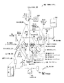
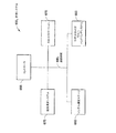
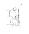
- 238000010586 diagram Methods 0.000 description 1
- 239000006185 dispersion Substances 0.000 description 1
- 239000002019 doping agent Substances 0.000 description 1
- 230000000694 effects Effects 0.000 description 1
- 230000005684 electric field Effects 0.000 description 1
- 238000005516 engineering process Methods 0.000 description 1
- 239000000284 extract Substances 0.000 description 1
- 238000001914 filtration Methods 0.000 description 1
- 238000010438 heat treatment Methods 0.000 description 1
- 239000007943 implant Substances 0.000 description 1
- 239000012535 impurity Substances 0.000 description 1
- 150000002500 ions Chemical class 0.000 description 1
- 230000001678 irradiating effect Effects 0.000 description 1
- 238000013178 mathematical model Methods 0.000 description 1
- 230000035515 penetration Effects 0.000 description 1
- 230000000704 physical effect Effects 0.000 description 1
- 238000012545 processing Methods 0.000 description 1
- 230000001902 propagating effect Effects 0.000 description 1
- 239000010453 quartz Substances 0.000 description 1
- 230000035945 sensitivity Effects 0.000 description 1
- 238000000926 separation method Methods 0.000 description 1
- 229910021332 silicide Inorganic materials 0.000 description 1
- FVBUAEGBCNSCDD-UHFFFAOYSA-N silicide(4-) Chemical compound [Si-4] FVBUAEGBCNSCDD-UHFFFAOYSA-N 0.000 description 1
- VYPSYNLAJGMNEJ-UHFFFAOYSA-N silicon dioxide Inorganic materials O=[Si]=O VYPSYNLAJGMNEJ-UHFFFAOYSA-N 0.000 description 1
- 210000002784 stomach Anatomy 0.000 description 1
- 239000000126 substance Substances 0.000 description 1
- 238000000427 thin-film deposition Methods 0.000 description 1
- 239000010936 titanium Substances 0.000 description 1
- 229910052719 titanium Inorganic materials 0.000 description 1
- 238000003949 trap density measurement Methods 0.000 description 1
Images


Classifications
-
- G—PHYSICS
- G01—MEASURING; TESTING
- G01R—MEASURING ELECTRIC VARIABLES; MEASURING MAGNETIC VARIABLES
- G01R31/00—Arrangements for testing electric properties; Arrangements for locating electric faults; Arrangements for electrical testing characterised by what is being tested not provided for elsewhere
- G01R31/28—Testing of electronic circuits, e.g. by signal tracer
- G01R31/2851—Testing of integrated circuits [IC]
- G01R31/2855—Environmental, reliability or burn-in testing
- G01R31/2856—Internal circuit aspects, e.g. built-in test features; Test chips; Measuring material aspects, e.g. electro migration [EM]
- G01R31/2858—Measuring of material aspects, e.g. electro-migration [EM], hot carrier injection
-
- G—PHYSICS
- G01—MEASURING; TESTING
- G01N—INVESTIGATING OR ANALYSING MATERIALS BY DETERMINING THEIR CHEMICAL OR PHYSICAL PROPERTIES
- G01N21/00—Investigating or analysing materials by the use of optical means, i.e. using sub-millimetre waves, infrared, visible or ultraviolet light
- G01N21/17—Systems in which incident light is modified in accordance with the properties of the material investigated
- G01N21/1702—Systems in which incident light is modified in accordance with the properties of the material investigated with opto-acoustic detection, e.g. for gases or analysing solids
-
- G—PHYSICS
- G01—MEASURING; TESTING
- G01N—INVESTIGATING OR ANALYSING MATERIALS BY DETERMINING THEIR CHEMICAL OR PHYSICAL PROPERTIES
- G01N21/00—Investigating or analysing materials by the use of optical means, i.e. using sub-millimetre waves, infrared, visible or ultraviolet light
- G01N21/84—Systems specially adapted for particular applications
- G01N21/88—Investigating the presence of flaws or contamination
- G01N21/95—Investigating the presence of flaws or contamination characterised by the material or shape of the object to be examined
- G01N21/9501—Semiconductor wafers
-
- G—PHYSICS
- G01—MEASURING; TESTING
- G01R—MEASURING ELECTRIC VARIABLES; MEASURING MAGNETIC VARIABLES
- G01R31/00—Arrangements for testing electric properties; Arrangements for locating electric faults; Arrangements for electrical testing characterised by what is being tested not provided for elsewhere
- G01R31/28—Testing of electronic circuits, e.g. by signal tracer
- G01R31/282—Testing of electronic circuits specially adapted for particular applications not provided for elsewhere
- G01R31/2831—Testing of materials or semi-finished products, e.g. semiconductor wafers or substrates
-
- G—PHYSICS
- G01—MEASURING; TESTING
- G01N—INVESTIGATING OR ANALYSING MATERIALS BY DETERMINING THEIR CHEMICAL OR PHYSICAL PROPERTIES
- G01N21/00—Investigating or analysing materials by the use of optical means, i.e. using sub-millimetre waves, infrared, visible or ultraviolet light
- G01N21/17—Systems in which incident light is modified in accordance with the properties of the material investigated
- G01N21/1702—Systems in which incident light is modified in accordance with the properties of the material investigated with opto-acoustic detection, e.g. for gases or analysing solids
- G01N2021/1706—Systems in which incident light is modified in accordance with the properties of the material investigated with opto-acoustic detection, e.g. for gases or analysing solids in solids
-
- G—PHYSICS
- G01—MEASURING; TESTING
- G01R—MEASURING ELECTRIC VARIABLES; MEASURING MAGNETIC VARIABLES
- G01R31/00—Arrangements for testing electric properties; Arrangements for locating electric faults; Arrangements for electrical testing characterised by what is being tested not provided for elsewhere
- G01R31/28—Testing of electronic circuits, e.g. by signal tracer
- G01R31/302—Contactless testing
- G01R31/308—Contactless testing using non-ionising electromagnetic radiation, e.g. optical radiation
- G01R31/311—Contactless testing using non-ionising electromagnetic radiation, e.g. optical radiation of integrated circuits
Landscapes
- Physics & Mathematics (AREA)
- Engineering & Computer Science (AREA)
- General Physics & Mathematics (AREA)
- Biochemistry (AREA)
- Analytical Chemistry (AREA)
- Chemical & Material Sciences (AREA)
- General Health & Medical Sciences (AREA)
- Life Sciences & Earth Sciences (AREA)
- Immunology (AREA)
- Pathology (AREA)
- Health & Medical Sciences (AREA)
- General Engineering & Computer Science (AREA)
- Computer Hardware Design (AREA)
- Microelectronics & Electronic Packaging (AREA)
- Environmental & Geological Engineering (AREA)
- Testing Or Measuring Of Semiconductors Or The Like (AREA)
- Investigating Or Analyzing Materials By The Use Of Ultrasonic Waves (AREA)
- Measurement Of Resistance Or Impedance (AREA)
- Measurement Of Length, Angles, Or The Like Using Electric Or Magnetic Means (AREA)
- Length Measuring Devices Characterised By Use Of Acoustic Means (AREA)
- Length Measuring Devices With Unspecified Measuring Means (AREA)
- Investigating Or Analysing Materials By Optical Means (AREA)
Applications Claiming Priority (2)
| Application Number | Priority Date | Filing Date | Title |
|---|---|---|---|
| US11/104,093 US7372584B2 (en) | 2005-04-11 | 2005-04-11 | Dual photo-acoustic and resistivity measurement system |
| PCT/US2006/010616 WO2006110282A2 (en) | 2005-04-11 | 2006-03-22 | Dual photo-acoustic and resistivity measurement system |
Publications (2)
| Publication Number | Publication Date |
|---|---|
| JP2008537781A true JP2008537781A (ja) | 2008-09-25 |
| JP2008537781A5 JP2008537781A5 (enExample) | 2011-12-08 |
Family
ID=37082851
Family Applications (1)
| Application Number | Title | Priority Date | Filing Date |
|---|---|---|---|
| JP2008505351A Pending JP2008537781A (ja) | 2005-04-11 | 2006-03-22 | デュアル光音響および抵抗測定システム |
Country Status (4)
| Country | Link |
|---|---|
| US (1) | US7372584B2 (enExample) |
| EP (1) | EP1869430A2 (enExample) |
| JP (1) | JP2008537781A (enExample) |
| WO (1) | WO2006110282A2 (enExample) |
Cited By (1)
| Publication number | Priority date | Publication date | Assignee | Title |
|---|---|---|---|---|
| JP2014077782A (ja) * | 2012-09-20 | 2014-05-01 | National Institute Of Advanced Industrial & Technology | 焼き入れ深さ測定装置、焼き入れ深さ測定方法、表層深さ測定装置、表層深さ測定方法 |
Families Citing this family (7)
| Publication number | Priority date | Publication date | Assignee | Title |
|---|---|---|---|---|
| FR2887334B1 (fr) * | 2005-06-20 | 2007-08-24 | Centre Nat Rech Scient | Dispositif et procede de caracterisation de structure par effet de longueur d'onde dans un systeme photo-acoustique |
| US20070024870A1 (en) * | 2005-08-01 | 2007-02-01 | Girard Mark T | Apparatuses and methods for measuring head suspensions and head suspension assemblies |
| DE202010006062U1 (de) * | 2010-04-23 | 2010-07-22 | Helmut Fischer GmbH Institut für Elektronik und Messtechnik | Messsonde zur zerstörungsfreien Messung der Dicke dünner Schichten |
| CN102288825A (zh) * | 2011-06-08 | 2011-12-21 | 沈阳飞机工业(集团)有限公司 | 碳纤维复合材料制件表面铝层电阻值测量方法 |
| GB2503722A (en) * | 2012-07-06 | 2014-01-08 | Sonex Metrology Ltd | A photoacoustic inspection device |
| US9093335B2 (en) * | 2012-11-29 | 2015-07-28 | Taiwan Semiconductor Manufacturing Company, Ltd. | Calculating carrier concentrations in semiconductor Fins using probed resistance |
| US11668644B2 (en) | 2021-03-30 | 2023-06-06 | Onto Innovation Inc. | Opto-acoustic measurement of a transparent film stack |
Citations (5)
| Publication number | Priority date | Publication date | Assignee | Title |
|---|---|---|---|---|
| JPS6370102A (ja) * | 1986-09-10 | 1988-03-30 | Mitsubishi Petrochem Co Ltd | 導電体肉厚非破壊測定法 |
| JPS6375808U (enExample) * | 1986-11-06 | 1988-05-20 | ||
| JPH09263934A (ja) * | 1996-03-29 | 1997-10-07 | Toppan Printing Co Ltd | 膜形成方法及びその装置 |
| JP2002516985A (ja) * | 1998-05-28 | 2002-06-11 | コーニンクレッカ フィリップス エレクトロニクス エヌ ヴィ | 少なくとも一つの層を含む構造の特徴を測定する方法及び装置 |
| JP2004325217A (ja) * | 2003-04-24 | 2004-11-18 | Nikon Corp | 搬送装置 |
Family Cites Families (15)
| Publication number | Priority date | Publication date | Assignee | Title |
|---|---|---|---|---|
| US3416078A (en) * | 1965-07-08 | 1968-12-10 | Motorola Inc | Method of determining resistivity of a thin layer |
| US3609537A (en) * | 1969-04-01 | 1971-09-28 | Ibm | Resistance standard |
| NL7008274A (enExample) * | 1970-06-06 | 1971-12-08 | ||
| US3676775A (en) * | 1971-05-07 | 1972-07-11 | Ibm | Method for measuring resistivity |
| US3783375A (en) * | 1973-02-21 | 1974-01-01 | Westinghouse Electric Corp | Means for calibrating a four-probe resistivity measuring device |
| US4710030A (en) * | 1985-05-17 | 1987-12-01 | Bw Brown University Research Foundation | Optical generator and detector of stress pulses |
| US5379109A (en) * | 1992-06-17 | 1995-01-03 | The United States Of America As Represented By The Secretary Of The Navy | Method and apparatus for non-destructively measuring local resistivity of semiconductors |
| TW280928B (enExample) * | 1994-10-24 | 1996-07-11 | At & T Corp | |
| US5546811A (en) * | 1995-01-24 | 1996-08-20 | Massachusetts Instittue Of Technology | Optical measurements of stress in thin film materials |
| US6008906A (en) * | 1995-08-25 | 1999-12-28 | Brown University Research Foundation | Optical method for the characterization of the electrical properties of semiconductors and insulating films |
| US5748318A (en) * | 1996-01-23 | 1998-05-05 | Brown University Research Foundation | Optical stress generator and detector |
| US5844684A (en) * | 1997-02-28 | 1998-12-01 | Brown University Research Foundation | Optical method for determining the mechanical properties of a material |
| US6038026A (en) * | 1998-07-07 | 2000-03-14 | Brown University Research Foundation | Apparatus and method for the determination of grain size in thin films |
| US6393915B1 (en) * | 1999-07-29 | 2002-05-28 | Koninklijke Philips Electronics N.V. | Method and device for simultaneously measuring multiple properties of multilayer films |
| US7050160B1 (en) * | 2002-10-11 | 2006-05-23 | Kla-Tencor Technologies Corporation | Process and apparatus for integrating sheet resistance measurements and reflectance measurements of a thin film in a common apparatus |
-
2005
- 2005-04-11 US US11/104,093 patent/US7372584B2/en not_active Expired - Lifetime
-
2006
- 2006-03-22 JP JP2008505351A patent/JP2008537781A/ja active Pending
- 2006-03-22 WO PCT/US2006/010616 patent/WO2006110282A2/en not_active Ceased
- 2006-03-22 EP EP06739420A patent/EP1869430A2/en not_active Withdrawn
Patent Citations (5)
| Publication number | Priority date | Publication date | Assignee | Title |
|---|---|---|---|---|
| JPS6370102A (ja) * | 1986-09-10 | 1988-03-30 | Mitsubishi Petrochem Co Ltd | 導電体肉厚非破壊測定法 |
| JPS6375808U (enExample) * | 1986-11-06 | 1988-05-20 | ||
| JPH09263934A (ja) * | 1996-03-29 | 1997-10-07 | Toppan Printing Co Ltd | 膜形成方法及びその装置 |
| JP2002516985A (ja) * | 1998-05-28 | 2002-06-11 | コーニンクレッカ フィリップス エレクトロニクス エヌ ヴィ | 少なくとも一つの層を含む構造の特徴を測定する方法及び装置 |
| JP2004325217A (ja) * | 2003-04-24 | 2004-11-18 | Nikon Corp | 搬送装置 |
Cited By (1)
| Publication number | Priority date | Publication date | Assignee | Title |
|---|---|---|---|---|
| JP2014077782A (ja) * | 2012-09-20 | 2014-05-01 | National Institute Of Advanced Industrial & Technology | 焼き入れ深さ測定装置、焼き入れ深さ測定方法、表層深さ測定装置、表層深さ測定方法 |
Also Published As
| Publication number | Publication date |
|---|---|
| WO2006110282A3 (en) | 2007-03-15 |
| WO2006110282A2 (en) | 2006-10-19 |
| US7372584B2 (en) | 2008-05-13 |
| EP1869430A2 (en) | 2007-12-26 |
| US20060227342A1 (en) | 2006-10-12 |
Similar Documents
| Publication | Publication Date | Title |
|---|---|---|
| US5748317A (en) | Apparatus and method for characterizing thin film and interfaces using an optical heat generator and detector | |
| US6175416B1 (en) | Optical stress generator and detector | |
| US5748318A (en) | Optical stress generator and detector | |
| US6348967B1 (en) | Method and device for measuring the thickness of opaque and transparent films | |
| US6504618B2 (en) | Method and apparatus for decreasing thermal loading and roughness sensitivity in a photoacoustic film thickness measurement system | |
| US5228776A (en) | Apparatus for evaluating thermal and electrical characteristics in a sample | |
| US20220364850A1 (en) | Second-harmonic generation for critical dimensional metrology | |
| CN1662808B (zh) | 用于检测不透明膜层埋覆缺陷的光学技术 | |
| EP1417450B1 (en) | Method and apparatus for increasing signal to noise ratio in a photoacoustic film thickness measurement system | |
| KR20020079727A (ko) | 집적 회로들의 특성화를 위한 광학적 방법 | |
| CN106077956A (zh) | 一种去除薄膜或涂层的激光加工方法及设备 | |
| CN105453243A (zh) | 光声基底评估系统和方法 | |
| JP2008537781A (ja) | デュアル光音響および抵抗測定システム | |
| JP2008537781A5 (enExample) | ||
| JP4025369B2 (ja) | 材料の機械的特性を判別する光学方法 | |
| EP4540576A1 (en) | Dimensional metrology using non-linear optics | |
| Liu et al. | A novel method and device for solder joint quality inspection by using laser ultrasound | |
| Logan | Optical metrology of thin films | |
| Logan et al. | Microelectronic Film thickness determination using a laserbased ultrasonic technique | |
| CN120102464A (zh) | 一种基于激光超声的半导体材料激光剥片裂纹实时在线监测装置及方法 | |
| JP2001083068A (ja) | 近接場光学顕微鏡 |
Legal Events
| Date | Code | Title | Description |
|---|---|---|---|
| A621 | Written request for application examination |
Free format text: JAPANESE INTERMEDIATE CODE: A621 Effective date: 20090316 |
|
| A977 | Report on retrieval |
Free format text: JAPANESE INTERMEDIATE CODE: A971007 Effective date: 20110603 |
|
| A131 | Notification of reasons for refusal |
Free format text: JAPANESE INTERMEDIATE CODE: A131 Effective date: 20110613 |
|
| A601 | Written request for extension of time |
Free format text: JAPANESE INTERMEDIATE CODE: A601 Effective date: 20110908 |
|
| A602 | Written permission of extension of time |
Free format text: JAPANESE INTERMEDIATE CODE: A602 Effective date: 20110915 |
|
| A601 | Written request for extension of time |
Free format text: JAPANESE INTERMEDIATE CODE: A601 Effective date: 20111011 |
|
| A521 | Request for written amendment filed |
Free format text: JAPANESE INTERMEDIATE CODE: A523 Effective date: 20111013 |
|
| A524 | Written submission of copy of amendment under article 19 pct |
Free format text: JAPANESE INTERMEDIATE CODE: A524 Effective date: 20111013 |
|
| A602 | Written permission of extension of time |
Free format text: JAPANESE INTERMEDIATE CODE: A602 Effective date: 20111018 |
|
| A02 | Decision of refusal |
Free format text: JAPANESE INTERMEDIATE CODE: A02 Effective date: 20120305 |