JP2008503029A - Memory device including data retention latch - Google Patents
Memory device including data retention latch Download PDFInfo
- Publication number
- JP2008503029A JP2008503029A JP2007527283A JP2007527283A JP2008503029A JP 2008503029 A JP2008503029 A JP 2008503029A JP 2007527283 A JP2007527283 A JP 2007527283A JP 2007527283 A JP2007527283 A JP 2007527283A JP 2008503029 A JP2008503029 A JP 2008503029A
- Authority
- JP
- Japan
- Prior art keywords
- state
- bit line
- value
- output
- memory
- Prior art date
- Legal status (The legal status is an assumption and is not a legal conclusion. Google has not performed a legal analysis and makes no representation as to the accuracy of the status listed.)
- Pending
Links
Images


Classifications
-
- G—PHYSICS
- G11—INFORMATION STORAGE
- G11C—STATIC STORES
- G11C7/00—Arrangements for writing information into, or reading information out from, a digital store
- G11C7/10—Input/output [I/O] data interface arrangements, e.g. I/O data control circuits, I/O data buffers
-
- G—PHYSICS
- G11—INFORMATION STORAGE
- G11C—STATIC STORES
- G11C7/00—Arrangements for writing information into, or reading information out from, a digital store
- G11C7/10—Input/output [I/O] data interface arrangements, e.g. I/O data control circuits, I/O data buffers
- G11C7/1051—Data output circuits, e.g. read-out amplifiers, data output buffers, data output registers, data output level conversion circuits
- G11C7/106—Data output latches
-
- G—PHYSICS
- G11—INFORMATION STORAGE
- G11C—STATIC STORES
- G11C7/00—Arrangements for writing information into, or reading information out from, a digital store
- G11C7/10—Input/output [I/O] data interface arrangements, e.g. I/O data control circuits, I/O data buffers
- G11C7/1051—Data output circuits, e.g. read-out amplifiers, data output buffers, data output registers, data output level conversion circuits
- G11C7/1069—I/O lines read out arrangements
-
- G—PHYSICS
- G11—INFORMATION STORAGE
- G11C—STATIC STORES
- G11C7/00—Arrangements for writing information into, or reading information out from, a digital store
- G11C7/10—Input/output [I/O] data interface arrangements, e.g. I/O data control circuits, I/O data buffers
- G11C7/1078—Data input circuits, e.g. write amplifiers, data input buffers, data input registers, data input level conversion circuits
- G11C7/1087—Data input latches
-
- G—PHYSICS
- G11—INFORMATION STORAGE
- G11C—STATIC STORES
- G11C7/00—Arrangements for writing information into, or reading information out from, a digital store
- G11C7/10—Input/output [I/O] data interface arrangements, e.g. I/O data control circuits, I/O data buffers
- G11C7/1078—Data input circuits, e.g. write amplifiers, data input buffers, data input registers, data input level conversion circuits
- G11C7/1096—Write circuits, e.g. I/O line write drivers
-
- G—PHYSICS
- G11—INFORMATION STORAGE
- G11C—STATIC STORES
- G11C7/00—Arrangements for writing information into, or reading information out from, a digital store
- G11C7/12—Bit line control circuits, e.g. drivers, boosters, pull-up circuits, pull-down circuits, precharging circuits, equalising circuits, for bit lines
-
- G—PHYSICS
- G11—INFORMATION STORAGE
- G11C—STATIC STORES
- G11C8/00—Arrangements for selecting an address in a digital store
- G11C8/16—Multiple access memory array, e.g. addressing one storage element via at least two independent addressing line groups
Landscapes
- Engineering & Computer Science (AREA)
- Microelectronics & Electronic Packaging (AREA)
- Static Random-Access Memory (AREA)
Abstract
複数の対の相補ビット線(200,202)および複数のラッチ回路を含むメモリ素子。複数の対の相補ビット線の各対はメモリ・セル(31,37)の列と結合している。各ラッチ回路は、データ線と結合している入力と、データ線の値により相補ラッチ値を供給するための第1の出力および第2の出力とを含む。複数の各ラッチの場合、第1の出力は、第1のビット線の値が、メモリ素子の動作中、第1の出力により連続的に決まるように複数のうちの一対の第1のビット線と結合し、第2の出力は、第2のビット線の値が、メモリ素子の動作中、第2の出力により連続的に決まるように一対の第2のビット線と結合している。A memory device including a plurality of pairs of complementary bit lines (200, 202) and a plurality of latch circuits. Each pair of the plurality of pairs of complementary bit lines is coupled to a column of memory cells (31, 37). Each latch circuit includes an input coupled to the data line and a first output and a second output for providing a complementary latch value depending on the value of the data line. For each of the plurality of latches, the first output is a pair of first bit lines of the plurality such that the value of the first bit line is continuously determined by the first output during operation of the memory element. And the second output is coupled to a pair of second bit lines such that the value of the second bit line is continuously determined by the second output during operation of the memory element.
Description
本発明は、集積回路に関し、特にメモリ素子に関する。 The present invention relates to integrated circuits, and more particularly to memory devices.
多ポート・メモリ素子の場合には、メモリ読み出し動作およびメモリ書き込み動作は、このような動作を行うために必要な時間の長さにより重大な影響を受ける。書き込み動作中、入力データ・アサート時間は、メモリ素子の属性に関連する復号遅延により異なる場合がある。例えば、アサート時間が不十分な場合には、入力データの依存性に関連する不確実さにより、メモリ内に書き込み中の偽値データによりプロセッサが障害を起こす場合がある。 In the case of multi-port memory devices, memory read and memory write operations are significantly affected by the length of time required to perform such operations. During a write operation, the input data assert time may vary depending on the decoding delay associated with the attributes of the memory element. For example, if the assertion time is insufficient, the processor may fail due to false value data being written into memory due to uncertainties associated with input data dependencies.
それ故、メモリの性能を改善するメモリ設計が求められている。 Therefore, there is a need for memory designs that improve memory performance.
以下に本発明について説明するが、これは例示としてのものであって、本発明は添付の図面に限定されない。図面中、類似の参照番号は類似の要素を示す。
当業者であれば、図面中の要素は、簡単に明確に表示するためのものであって、必ずしも正確な縮尺でないことを理解することができるだろう。例えば、本発明の実施形態を容易に理解できるように、図面中の要素のうちのあるものの寸法は他の要素より誇張してある。
The present invention is described below by way of example, and the present invention is not limited to the attached drawings. In the drawings, like reference numbers indicate like elements.
Those skilled in the art will appreciate that the elements in the drawings are for simplicity and clarity and are not necessarily to scale. For example, the dimensions of some of the elements in the drawings are exaggerated over other elements so that embodiments of the invention can be readily understood.
一実施形態の場合には、メモリ素子は、ビット線と、メモリ・セルの列と、ラッチ回路とを含む。メモリ・セルの列はビット線と結合している。ラッチ回路は、データ線と結合している入力と、データ線の値によりラッチした値を供給する出力とを有する。出力は、ビット線の値が、メモリ素子の動作中出力により連続的に決まるようにビット線と結合している。 In one embodiment, the memory element includes a bit line, a column of memory cells, and a latch circuit. A column of memory cells is coupled to a bit line. The latch circuit has an input coupled to the data line and an output for supplying a value latched by the value of the data line. The output is coupled to the bit line such that the value of the bit line is continuously determined by the output during operation of the memory element.
一実施形態は、メモリ素子を動作するための方法に関する。メモリ・セルの列のメモリ・セルに対して、複数の読み出しおよび複数の書き込みが行われる。ビット線の値はメモリ・セルの列と結合していて、ビット線の値は、メモリ素子の動作中、ラッチ出力により連続的に制御される。一実施形態の場合には、ラッチ出力の値は、第1の状態から第2の状態へのクロック信号の状態の変化により決まる時点で、ラッチ入力の値に応じて変化することができる。一実施形態の場合には、値はメモリ・セルの列のメモリ・セルに書き込むことができる。この場合、書き込みは、例えば、ビット線の状態の変化を含む。一実施形態の場合には、値をメモリ・セルの列のメモリ・セルに書き込むことができる。この場合、書き込みは、例えば、非書込み状態から書込み状態への書込み線の状態の変化を含む。 One embodiment relates to a method for operating a memory device. Multiple reads and multiple writes are performed on the memory cells in the column of memory cells. The value of the bit line is coupled to the column of memory cells, and the value of the bit line is continuously controlled by the latch output during operation of the memory element. In one embodiment, the value of the latch output can change according to the value of the latch input at a time determined by the change in state of the clock signal from the first state to the second state. In one embodiment, the value can be written to a memory cell in the column of memory cells. In this case, writing includes, for example, a change in the state of the bit line. In one embodiment, values can be written to memory cells in a column of memory cells. In this case, writing includes, for example, a change in the state of the writing line from the non-writing state to the writing state.
一実施形態の場合には、メモリ素子は、ビット線と、メモリ・セルの列と、ラッチ回路とを含む。メモリ・セルの列はビット線と結合している。ラッチ回路は、データ線と結合している入力と、データ線の値によりラッチした値を供給するための出力とを有する。出力は、ビット線に接続している。 In one embodiment, the memory element includes a bit line, a column of memory cells, and a latch circuit. A column of memory cells is coupled to a bit line. The latch circuit has an input coupled to the data line and an output for providing a value latched by the value of the data line. The output is connected to the bit line.
一実施形態の場合には、メモリ素子は、複数の対の相補ビット線と、複数のラッチ回路とを含む。複数の対の相補ビット線の各対は、メモリ・セルの列と結合している。各ラッチ回路は、データ線と結合している入力と、データ線の値により相補ラッチ値を供給するための第1の出力および第2の出力とを有する。複数のラッチ回路の各ラッチの場合、第1の出力は、第1のビット線の値が、メモリ素子の動作中、第1の出力により連続的に決まるように複数の対の第1のビット線と結合していて、第2の出力は、第2のビット線の値が、メモリ素子の動作中、第2の出力により連続的に決まるように対の第2のビット線と結合している。 In one embodiment, the memory element includes a plurality of pairs of complementary bit lines and a plurality of latch circuits. Each pair of pairs of complementary bit lines is coupled to a column of memory cells. Each latch circuit has an input coupled to the data line and a first output and a second output for providing a complementary latch value depending on the value of the data line. For each latch of the plurality of latch circuits, the first output is the first bit of the plurality of pairs such that the value of the first bit line is continuously determined by the first output during operation of the memory element. The second output is coupled to the second bit line of the pair such that the value of the second bit line is continuously determined by the second output during operation of the memory element. Yes.
一実施形態の場合には、メモリ素子は、ビット線と、メモリ・セルの列と、ラッチ回路とを含む。メモリ・セルの列はビット線と結合している。ラッチ回路は、データ線と結合している入力と、データ線の値によりラッチした値を供給するための出力とを有する。出力は、メモリ素子の動作中、出力のところの値が変化した場合だけ、ビット線の値が変化するようにビット線と結合している。 In one embodiment, the memory element includes a bit line, a column of memory cells, and a latch circuit. A column of memory cells is coupled to a bit line. The latch circuit has an input coupled to the data line and an output for providing a value latched by the value of the data line. The output is coupled to the bit line such that the value of the bit line changes only when the value at the output changes during operation of the memory element.
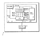
図1は、本発明の一実施形態による集積回路2である。集積回路2は、コア3と、バス・インタフェース・ユニット(BIU)6とを含む。コア3は、クロック回路4と、実行ユニット5と、メモリ制御装置7と、メモリ10とを含む。一実施形態の場合には、コア3は、例えば、プロセッサ・コアであってもよいし、メモリ10は、例えば、多ポート・レジスタ・ファイルにより特徴づけることができる。
FIG. 1 is an
一実施形態の場合には、集積回路2の正常な動作中、メモリ10に対して、実行ユニット5からメモリ制御装置7に供給される制御信号8に基づいて、書き込みアクセスまたは読み出しアクセスが行われる。制御信号8は、メモリ読み出し動作またはメモリ書き込み動作をスタートするために使用することができる。実行ユニット5は、例えば、メモリ10内にデータを格納し、メモリ10からデータを読み出すために、制御信号8を発行する中央処理装置(CPU)であっても、またはデジタル信号処理装置であってもよい。一実施形態の場合には、メモリ10にいつデータを書き込むことができるか、またはメモリ10からいつデータを読み出すことができるかを決定するためのタイミング機構として使用されているクロック信号29(CLK29)は、クロック回路4からメモリ制御装置7、実行ユニット5およびメモリ10に供給される。メモリ制御装置7は、実行ユニット5からクロック信号29および制御信号8を受信し、実行ユニット5により読み出し動作が要求されたのかまたは書き込み動作が要求されたのかに基づいて、書き込み動作可能信号60(WR EN60)または読み出し動作可能信号14(READ EN14)をアサートする。
In one embodiment, during normal operation of the integrated
読み出し動作中、RD ADDRESS15およびREAD EN14が、メモリ制御装置7からメモリ10に供給される。メモリ10は、READ EN14を受信し、RD ADDRESS15が指定するメモリ・アドレス位置を動作可能にする。RD ADDRESS15が指定するメモリ・アドレス位置内のデータはメモリ10から読み出され、データ線214を介してDATA−OUT212として実行ユニット5に供給される。
During the read operation, RD ADDRESS 15 and READ EN 14 are supplied from the
書き込み動作中、WR ADDRESS75およびWR EN60はメモリ制御装置7からメモリ10に供給される。メモリ10は、WR EN60を受信し、書き込み動作に対するWR ADDRESS75が指定するメモリ10内のメモリ・アドレス位置を動作可能にする。実行ユニット5からのデータ(DATA−IN211)は、データ線213を介してメモリ10に供給され、WR ADDRESS75が指定するメモリ10のメモリ・アドレス位置に書き込まれる。集積回路2は、他の実施形態の場合には他の構成を有することができる。
During the write operation, WR ADDRESS 75 and WR EN 60 are supplied from the
図2は、本発明の一実施形態によるメモリ10である。メモリ10は、読み出し行デコーダ13と、読み出しワード線ドライバ38と、書き込みワード線ドライバ39と、書き込みビット線ラッチ76と、列制御ロジック25と、列アレイ回路11と、列アレイ回路12と、インバータ70と、書き込み行デコーダ62と、列回路77とを含む。読み出しワード線ドライバ38は、読み出しワード線ドライバ16と、読み出しワード線ドライバ19と、読み出しワード線ドライバ22とを含む。書き込みワード線ドライバ39は、書き込みワード線ドライバ58と、書き込みワード線ドライバ61と、書き込みワード線ドライバ64とを含む。列アレイ回路11は、書き込みビット線ラッチ28と、ビットセル(メモリ・セル)31と、ビットセル34と、ビットセル37と、列回路40とを含む。列アレイ回路12は、書き込みビット線ラッチ43と、ビットセル46と、ビットセル49と、ビットセル52と、列回路55とを含む。説明を分かり易くするために、ビットセル46、ビットセル49、ビットセル52、ビットセル31、ビットセル34およびビットセル37をビットセル・アレイ69と呼ぶことにし、書き込みワード線ドライバ39および書き込み行デコーダ62をワード線発生回路と呼ぶことにする。図の実施形態の場合には、ビットセル31はビットセル46と同じ行に位置する。
FIG. 2 is a
一実施形態の場合には、読み出し動作中、メモリ10の読み出し行デコーダ13は、メモリ制御装置7(図1)から読み出し動作可能信号14および読み出しアドレス15を受信し、クロック回路4(図1)からクロック信号29を受信する。読み出し行デコーダ13は、読み出しアドレス15を復号し、読み出しアクセスができるようにビットセル・アレイ69のビット・セルの行を決定する。ビットセル・アレイ69は、ビット・セルの1つまたは複数の行または列を含むことができる。読み出し行デコーダ13は、行動作可能信号18を復号した行アドレスに対応する読み出しワード線ドライバ38のうちの少なくとも1つに出力する。復号した行アドレスに対応する読み出しワード線ドライバ38の読み出しワード線ドライバは、ビット・セルの選択した1つまたは複数の行に供給される読み出しワード線信号をアサートする。図の実施形態の場合には、読み出しワード線ドライバ16、読み出しワード線ドライバ19、または読み出しワード線ドライバ22が、読み出しワード線信号RWL0、RWL1、RWLNのいずれかをそれぞれアサートする。ビット・セルの選択した行は、読み出しビット線信号(RBL0およびRBLB0)を列回路40への入力として供給し、読み出しビット線信号(RBL1およびRBLB1)を列回路55への入力として供給する。ビット・セル・アレイ69が複数の行のビット・セルを有している場合には、読み出しビット線信号RBL0およびRBLB0および読み出しビット線信号RBL1およびRBLB1を列回路40および列回路55に入力として供給する前に、ビット・セルの1つまたは複数の追加行に供給することができる。同様に、ビット・セル・アレイ69がビット・セルの複数の列を有している場合に、読み出しワード線信号RWL0、RWL1およびRWLNをビット・セルの1つまたは複数の追加列に供給することができる。
In one embodiment, during the read operation, the
列回路40および列回路55は、それぞれ読み出しビット線信号RBL0およびRBLB0および読み出しビット線信号RBL1およびRBLB1を受信する。列回路40は、出力データ(DATA−OUT0およびDATA−OUTB0)を生成するために、読み出し線ビット信号RBL0およびRBLB0を使用し、列回路55は、出力データ(DATA−OUT1およびDATA−OUTB1)を生成するために、読み出しビット線信号を使用する。次に、出力データは、さらに処理を行うために図1の実行ユニット5のような実行ユニットに供給することができる。メモリ10の他の実施形態は、図2に示すものに限定されない1つの列アレイ回路11または複数の列アレイ回路を含むことができることに留意されたい。
一実施形態の場合には、書き込み動作中、書き込み行デコーダ62は、書き込み動作可能信号60、クロック信号29および書き込みアドレス75を受信する。書き込み行デコーダ62は書き込みアドレス75を復号し、ビット・セルのどの行を書き込みアクセスのために動作可能にするのかを決定する。書き込み行デコーダ62は、行動作可能信号68を復号した行アドレスに対応する書き込みワード線ドライバ39のうちの少なくとも1つに出力する。復号した行アドレスに対応する書き込みワード線ドライバ39の書き込みワード線ドライバは、ビット・セルの選択した1つまたは複数の行に供給される書き込みワード線信号をアサートする。図の実施形態の場合には、書き込みワード線ドライバ58、書き込みワード線ドライバ61、および書き込みワード線ドライバ64が、書き込みワード線ドライバ39をビットセル・アレイ69に結合する書き込みワード線を介して、書き込みワード線信号WWL0、WWL1およびWWLNのいずれかをそれぞれアサートする。一実施形態の場合には、書き込みワード線信号は、例えば、クロック信号29の状態の変化により決まる時点で、非書込み状態から書込み状態に変化することができる。例えば、実行ユニット5(図示せず)から供給することができる入力データ(DATA−IN0およびDATA−IN1)は、書き込みビット線ラッチ76(書き込みビット線ラッチ28および書き込みビット線ラッチ43)に転送される。書き込みビット線ラッチ76は、入力データおよびインバータ70により反転される反転クロック信号29(CLKB30)を受信する。書き込みビット線ラッチ76は、入力データを書き込みビット線信号WBL0、WBL1として、および書き込みビット線信号WBLB0、WBLBの補足を、書き込みビット線ラッチ76をビットセル・アレイ69と結合する書き込みビット線上に駆動するためにCLKB30を使用する。次に、書き込みビット線信号が、ビットセル・アレイ69のビットセルの選択した行上に書き込まれる。ビット・セル・アレイ69がビット・セルの複数の行を有している場合には、書き込みビット線信号WBL0およびWBLB0および書き込みビット線信号WBL1およびWBLB1を、ビット・セルの1つまたは複数の追加行に供給することができる。同様に、ビット・セル・アレイ69がビット・セルの複数の列を有している場合には、書き込みワード線信号WWL0、WWL1およびWWLNをビット・セルの1つまたは複数の追加列に供給することができる。メモリ10は、他の実施形態の場合には他の構成を有することができる。
In one embodiment, during a write operation, the
図3は、列アレイ回路11の一実施形態である。図に示すように、列アレイ回路11は、書き込みビット線ラッチ28と、ビットセル31と、ビットセル37と、列回路40とを含む。書き込みビット線ラッチ28は、書き込みビット線200および書き込みビット線202を介してビットセル31およびビットセル37と結合している。一実施形態の場合には、書き込みビット線202は、書き込みビット線200の相補ビット線である。ビットセル31およびビットセル37は、読み出しビット線204および読み出しビット線206を介して列回路40と結合している。他の実施形態の場合には、追加のビット・セルを列アレイ回路11に追加することができる。ビットセル34は図3には図示していない。
FIG. 3 is an embodiment of the
書き込み動作中、列アレイ回路11の書き込みビット線ラッチ28は、インバータ70(図2)からクロックバー信号30(CLKB30)を、実行ユニット5(図1)から入力データ(DATA−IN0)を受信する。NORゲート107は、DATA−IN0およびクロックバー信号30を否定論理和(NOR)し、その出力をNMOSトランジスタ119に供給する。NORゲート103は、クロックバー信号30および入力データDATA−IN0の逆数を否定論理和し、その出力をNMOSトランジスタ116に供給する。
During the write operation, the write
通常、DATA−IN0およびクロックバー信号30は、アサート値または非アサート値をとることができる。一実施形態の場合には、クロックバー信号30が高レベルの場合には、NORゲート107の出力およびNORゲート103の出力は低レベルである。その結果、NMOSトランジスタ119およびNMOSトランジスタ116はオフになり、インバータ113とクロス結合しているインバータ110を含むラッチ180は、もしあった場合には、ラッチ180に前に書き込んだデータ値を能動的に保持する。
In general, DATA-IN0 and
一実施形態の場合には、クロックバー信号30が低レベルであり、DATA−IN0が高レベルである場合には、NORゲート107の出力は低レベルであり、NORゲート103の出力は高レベルである。その結果、NMOSトランジスタ119はオフになり、NMOSトランジスタ116はオンになり、ノード114は低レベルであり、インバータ110の出力は高レベルである。インバータ110の出力は、インバータ113およびインバータ124により反転される。インバータ113は、インバータ110の出力を反転し、その出力をインバータ127に供給する。書き込みビット線信号WBL0としての書き込みビット線200上で転移するインバータ127の出力は高レベルである。書き込みビット線バー信号WBLB0としての書き込みビット線202上で転移するインバータ124の出力は低レベルである。両方の書き込みビット線信号WBL0および書き込みビット線バー信号WBLB0はビットセル31に供給される。
In one embodiment, when the
一実施形態の場合には、クロックバー信号30が低レベルであり、DATA−IN0が低レベルである場合には、NORゲート107の出力は高レベルであり、NORゲート103の出力は低レベルである。その結果、NMOSトランジスタ119がオンになり、NMOSトランジスタ116がオフになる。NMOSトランジスタ119がオンになるので、ノード115が低レベルになり、インバータ113の出力は高レベルになる。書き込みビット線バー信号WBLB0として書き込みビット線202上で転移するインバータ124の出力は高レベルであり、書き込みビット線バー信号WBL0として書き込みビット線204に転移するインバータ127の出力は低レベルである。それ故、書き込みビット線ラッチ28の出力のところの書き込みビット線信号WBL0および書き込みビット線バー信号WBLB0の値は、クロックバー信号30の状態の変化により決まる時点での入力データ線のところのDATA−IN0の値による値を変える。同様に、書き込みビット線200および書き込みビット線202の書き込みビット線信号WBL0および書き込みビット線バー信号WBLB0の値は、クロック信号の状態の変化により決まる時点での入力データ線上のDATA−IN0の値に応じて変化することができる。書き込みビット線信号WBL0および書き込みビット線バー信号WBLB0は、ビットセル31に供給される。
In one embodiment, when the
ビットセル31は、NMOSトランジスタ133の電流端子のところでインバータ127の出力から書き込みビット信号WBL0を受信し、NMOSトランジスタ136の電流端子のところでインバータ124の出力から書き込みビット線バ−信号WBLB0を受信する。NMOSトランジスタ133およびNMOSトランジスタ136の制御端子に供給される書き込みワード線信号WWL0が高レベルである場合には、NMOSトランジスタ133およびNMOSトランジスタ136がオンになる。ノード122は書き込みビット線200に転移された値になり、ノード123は、書き込みビット線202に転移された値になる。それ故、WWL0が高レベルである場合には、ビットセル31は、列アレイ回路11内へ入力として供給される入力データDATA−IN0を格納する。WWL0が低レベルである場合には、NMOSトランジスタ133およびNMOSトランジスタ136がオフなり、書き込みビット線200および書き込みビット線202から書き込まれたデータ値が、インバータ121およびインバータ130により格納される。
Bit cell 31 receives write bit signal WBL0 from the output of
読み出し動作中、読み出しワード線208上の読み出しワード線信号RWL0が高レベルである場合には、NMOSトランジスタ139およびNMOSトランジスタ145がオンになる。ノード122のところに格納している値の逆数およびノード123のところに格納している値の逆数が、それぞれNMOSトランジスタ142およびNMOSトランジスタ148により、読み出しビット線バー信号RBLB0として読み出しビット線204に転送され、読み出しビット線信号RBL0として読み出しビット線206に転送される。列回路40へ入力として供給される予備充電信号(PCH)が高レベルである場合には、PMOSトランジスタ151およびPMOSトランジスタ154がオフになり、読み出しビット線204上の読み出しビット線信号RBLB0の値がインバータ157に供給され、読み出しビット線206上の読み出しビット線信号RBL0の値がインバータ163に供給される。インバータ157の出力は、出力データDATA−OUT0として実行ユニット(図示せず)およびPMOSトランジスタ160の制御端子に供給される。同様に、インバータ163の出力は、出力データ(DATA−OUTB0)として実行ユニット(図示せず)およびPMOSトランジスタ166の制御端子に供給される。読み出しビット線信号RBL0および読み出しビット線信号RBLB0の値により、PMOSトランジスタ160またはPMOSトランジスタ166をオフにすることができる。他の実施形態の場合には、書き込みビット線ラッチ28、ビットセル31、ビットセル37、および/または列回路40は、他の構成を有することができる。図の実施形態の場合には、DATA−IN0信号は、シングル・エンド信号であるが、他の実施形態の場合には、この信号は差動信号のような他の形の信号であってもよい。
During the read operation, when the read word line signal RWL0 on the read word line 208 is at a high level, the
図4は、本発明の一実施形態によるビットセル31に対して読み出しおよび書き込みを行うための種々の信号を示すタイミング図である。一実施形態に示すように、読み出し動作中、読み出し動作可能信号14およびクロック信号29が高レベルである場合には、読み出しワード線信号RWL0は高レベルである。読み出しワード線信号RWL0は、例えば、読み出し行デコーダ13および読み出しワード線ドライバ38により遅延が生じた場合には、高レベルであるとアサートすることができる。読み出しワード線信号RWL0が高レベルになると、読み出しビット線信号RBL0が低レベルになり、読み出しビット線バー信号RBLB0が高レベルになるか、または読み出しビット線信号RBL0が高レベルになり、読み出しビット線バー信号RBLB0が低レベルになる。読み出しビット線信号RBL0または読み出しビット線バー信号RBLB0が低レベルになると、DATA−OUT0またはDATA−OUTB0が高レベルになる。クロック信号29が低レベルである場合には、読み出しワード線信号RWL0が低レベルであり、読み出しビット線信号RBL0および読み出しビット線バー信号RBLB0が高レベルであり、DATA−OUT0およびDATA−OUTB0が低レベルである。
FIG. 4 is a timing diagram illustrating various signals for reading and writing to the bitcell 31 according to one embodiment of the present invention. As shown in one embodiment, during the read operation, when the read enable
図4に示すように、DATA−IN0およびクロック信号29が高レベル(クロックバー信号30が低レベル)である場合には、書き込みビット線信号WBL0が高レベルであり、書き込みビット線バー信号WBLB0が低レベルである。書き込み動作中、書き込み動作可能信号60およびクロック信号29が高レベルである場合には、書き込みワード線信号WWL0は高レベルである。書き込みワード線信号WWL0は、例えば、書き込み行デコーダ62および書き込みワード線ドライバ39により遅延が生じた場合には、高レベルであるとアサートすることができる。クロック信号29が低レベルである場合には、書き込みワード線信号WWL0は低レベルになる。
As shown in FIG. 4, when DATA-IN0 and
図4のタイミング図を見れば分かるように、復号遅延は、書き込みワード線信号WWL0のアサートへのクロック信号29のアサートに関連する。ラッチ遅延は、書き込みビット線信号WBL0のアサートへのクロック信号29のアサートに関連する。一実施形態の場合には、書き込み動作中、書き込みビット線信号WBL0は、書き込みワード線信号WWL0が低レベルになるまで高い値に保持される。同様に、書き込みビット線バー信号WBLB0は、書き込みワード線信号WWL0が低レベルになるまで低い値に保持される。DATA−IN0は、クロック信号29が低レベルになるまで高レベルに保持される。図に示すように、DATA−IN0アサート時間は、書き込みワード線信号WWL0に関連する復号遅延の影響を受けない。
As can be seen from the timing diagram of FIG. 4, the decoding delay is related to the assertion of the
今まで特定の実施形態を参照しながら本発明を説明してきたが、通常の当業者であれば、下記の特許請求の範囲に記載する本発明の範囲から逸脱することなしに種々の修正および変更を行うことができることを理解することができるだろう。それ故、上記明細書および図面は本発明を制限するものではなく、例示としてのものと見なすべきであり、このようなすべての修正は本発明の範囲内に含まれる。 Although the invention has been described with reference to specific embodiments, those skilled in the art will recognize that various modifications and changes can be made without departing from the scope of the invention as set forth in the claims below. You will be able to understand that you can do that. Therefore, the above specification and drawings should not be construed as limiting the invention, but as examples, and all such modifications are included within the scope of the invention.
特定の実施形態を参照しながら種々の利益、種々の他の利点および問題の解決方法を説明してきたが、このような種々の利益、種々の他の利点、問題の解決方法および任意の利益、利点または問題の解決方法を実行し、より優れたものにすることができる任意の要素は、請求項のいずれかまたはすべての重要で、必要なまたは不可欠な機能または要素であると解釈すべきではない。 While various benefits, various other advantages and solutions to problems have been described with reference to particular embodiments, such various benefits, various other advantages, solutions to problems and optional benefits, Any element that can perform an advantage or solve a problem and make it better should not be construed as an important, necessary or essential function or element of any or all of the claims. Absent.
Claims (34)
ビット線と、
同ビット線と結合しているメモリ・セルの列と、
データ線と結合している入力および同データ線の値によりラッチされた値を供給する出力を有するラッチ回路と、を備え、
前記出力は前記ビット線と結合して、メモリ素子の動作中、前記ビット線の値が前記出力により連続的に決まる、メモリ素子。 A memory element,
Bit lines,
A column of memory cells coupled to the bit line;
A latch circuit having an input coupled to the data line and an output for providing a value latched by the value of the data line;
The output is coupled to the bit line, and the value of the bit line is continuously determined by the output during operation of the memory element.
前記ラッチ回路の出力が、前記一対のインバータの第1のインバータの入力および前記一対のインバータの第2のインバータの出力と結合している請求項1に記載のメモリ素子。 The latch circuit includes a pair of cross-coupled inverters;
The memory element according to claim 1, wherein an output of the latch circuit is coupled to an input of a first inverter of the pair of inverters and an output of a second inverter of the pair of inverters.
前記書き込み信号を供給するために前記ワード線と結合している出力を有し、クロック信号を受信するための入力を含むワード線生成回路とをさらに備え、前記書き込み信号が、前記ワード線生成回路の前記入力のところで受信する前記クロック信号の状態の変化により決まる時点で状態を変化させ、
前記ワード線生成回路が受信するクロック信号および前記ラッチの第2の入力のところで受信するクロック信号が、共通のクロック信号により生成される請求項8に記載のメモリ素子。 A word line coupled to a memory cell in the column of memory cells to send a write signal to the memory cell;
A word line generation circuit having an output coupled to the word line for supplying the write signal and including an input for receiving a clock signal, wherein the write signal is the word line generation circuit Change state at a time determined by a change in state of the clock signal received at the input of
9. The memory element according to claim 8, wherein the clock signal received by the word line generation circuit and the clock signal received at the second input of the latch are generated by a common clock signal.
前記書き込み信号が、前記第1の状態から前記第2の状態への共通のクロック信号の状態の変化により決まる時点で非書込み状態から書込み状態に変化する請求項10に記載のメモリ素子。 The value at the output of the latch circuit is changed according to the value of the data line at the time determined by the change in the state of the common clock signal from the first state to the second state,
The memory device according to claim 10, wherein the write signal changes from a non-write state to a write state at a time determined by a change in state of a common clock signal from the first state to the second state.
前記第2のビット線と結合しているメモリ・セルの第2の列と、
第2のデータ線と結合している第2の入力と、前記第2のデータ線の値によりラッチされた値を供給する第2の出力とを有する第2のラッチ回路とをさらに備え、
前記第2のラッチ回路の第2の出力が前記第2のビット線と結合して、メモリ素子の動作中に、前記第2のビット線の値が前記第2の出力により連続的に決まる請求項1に記載のメモリ素子。 A second bit line;
A second column of memory cells coupled to the second bit line;
A second latch circuit having a second input coupled to the second data line and a second output for providing a value latched by the value of the second data line;
The second output of the second latch circuit is coupled to the second bit line, and the value of the second bit line is continuously determined by the second output during operation of the memory element. Item 2. The memory element according to Item 1.
前記動作中、ラッチ出力により、前記メモリ・セルの列と結合しているビット線の値を連続的に制御するステップと、を含むメモリ素子を動作するための方法。 Operating a memory device including performing a plurality of reads and writes to a memory cell in a column of memory cells;
Continuously controlling a value of a bit line coupled to the column of memory cells with a latch output during the operation.
前記書込み線の前記状態を変化させる前記ステップが、前記第1の状態から前記第2の状態へのクロック信号の状態の変化により決まる時点で、前記状態を変化させるステップをさらに含む請求項23に記載の方法。 The step of changing the state of the bit line comprises changing the state at a time determined by a change in state of the clock signal from a first state to a second state;
24. The method of claim 23, further comprising the step of changing the state at a time when the step of changing the state of the write line is determined by a change in state of a clock signal from the first state to the second state. The method described.
前記書き込みステップの後で、前記メモリ・セルの列のメモリ・セルにもう1つの値を書き込むステップをさらに含み、もう1つの値を書き込む同ステップが、前記ビット線の状態を変化させるステップを含み、前記書き込みおよびもう1つの値の書き込みの状態の変化の間に前記列のメモリ・セルへ他の書き込みが行われず、
前記ビット線が、前記書き込みの状態の変化の時点からもう1つの値の書き込みの状態の変化まで、前記第2の状態のままである請求項22に記載の方法。 The writing step includes changing the state of the bit line from a first state to a second state;
After the writing step, the method further includes a step of writing another value to a memory cell in the column of the memory cell, and the step of writing another value includes changing the state of the bit line. No other writes to the memory cells in the column during the write and another value write state change,
23. The method according to claim 22, wherein the bit line remains in the second state from the time of the change of the write state to the change of the write state of another value.
動作中、第2のラッチ出力によりメモリ・セルの第2の列と結合している第2のビット線の値を連続的に制御するステップをさらに含む請求項20に記載の方法。 The step of operating the memory element further comprises performing a plurality of reads and writes to memory cells in a second column of memory cells;
21. The method of claim 20, further comprising continuously controlling a value of a second bit line coupled to a second column of memory cells with a second latch output during operation.
ビット線と、
前記ビット線と結合しているメモリ・セルの列と、
データ線と結合している入力と、前記データ線の値によりラッチされた値を供給する出力とを有するラッチ回路とを備え、前記出力が前記ビット線に接続しているメモリ素子。 A memory element,
Bit lines,
A column of memory cells coupled to the bit line;
A memory device comprising: a latch circuit having an input coupled to a data line; and an output for supplying a value latched by the value of the data line, the output connected to the bit line.
前記第2のビット線と結合しているメモリ・セルの第2の列と、
第2のデータ線と結合している第2の入力と、前記第2のデータ線の値によりラッチされた値を供給する第2の出力とを有する第2のラッチ回路とをさらに備え、前記第2の出力が、前記第2のビット線に接続している請求項31に記載のメモリ素子。 A second bit line;
A second column of memory cells coupled to the second bit line;
A second latch circuit having a second input coupled to a second data line and a second output for providing a value latched by a value of the second data line; 32. The memory device according to claim 31, wherein a second output is connected to the second bit line.
複数の対の相補ビット線であって、各対がメモリ・セルの列と結合している複数の対の相補ビット線と、
複数のラッチ回路であって、各ラッチ回路がデータ線と結合している入力と、前記データ線の値により相補ラッチ値を供給するための第1の出力および第2の出力とを含む複数のラッチ回路とを備え、
前記複数の各ラッチに対して、前記第1の出力が、前記第1のビット線の値が、メモリ素子の動作中、前記第1の出力により連続的に決まるように前記複数の対の一対の第1のビット線と結合し、前記第2の出力が、前記第2のビット線の値が、メモリ素子の動作中、前記第2の出力により連続的に決まるように前記対の第2のビット線と結合しているメモリ素子。 A memory element,
A plurality of pairs of complementary bit lines, each pair coupled to a column of memory cells;
A plurality of latch circuits, each including an input coupled to a data line, and a first output and a second output for supplying a complementary latch value according to the value of the data line; And a latch circuit,
For each of the plurality of latches, the first output is a pair of the plurality of pairs such that the value of the first bit line is continuously determined by the first output during operation of the memory element. And the second output of the pair of second bit lines is such that the value of the second bit line is continuously determined by the second output during operation of the memory element. Memory element coupled to the bit line of.
ビット線と、
前記ビット線と結合しているメモリ・セルの列と、
データ線と結合している入力と、前記データ線の値によりラッチされた値を供給する出力とを有するラッチ回路とを備え、前記出力が、メモリ素子の動作中、前記出力のところの値が変化した場合だけ、前記ビット線の前記値が変化するように前記ビット線と結合しているメモリ素子。 A memory element,
Bit lines,
A column of memory cells coupled to the bit line;
A latch circuit having an input coupled to the data line and an output for supplying a value latched by the value of the data line, the value at the output being during operation of the memory element. A memory device coupled to the bit line such that the value of the bit line changes only when it changes.
Applications Claiming Priority (2)
| Application Number | Priority Date | Filing Date | Title |
|---|---|---|---|
| US10/865,274 US7349266B2 (en) | 2004-06-10 | 2004-06-10 | Memory device with a data hold latch |
| PCT/US2005/015858 WO2006001910A2 (en) | 2004-06-10 | 2005-05-05 | Memory device with a data hold latch |
Publications (2)
| Publication Number | Publication Date |
|---|---|
| JP2008503029A true JP2008503029A (en) | 2008-01-31 |
| JP2008503029A5 JP2008503029A5 (en) | 2008-06-26 |
Family
ID=35505511
Family Applications (1)
| Application Number | Title | Priority Date | Filing Date |
|---|---|---|---|
| JP2007527283A Pending JP2008503029A (en) | 2004-06-10 | 2005-05-05 | Memory device including data retention latch |
Country Status (6)
| Country | Link |
|---|---|
| US (1) | US7349266B2 (en) |
| EP (1) | EP1915502A4 (en) |
| JP (1) | JP2008503029A (en) |
| KR (1) | KR20070029193A (en) |
| CN (1) | CN101023237B (en) |
| WO (1) | WO2006001910A2 (en) |
Families Citing this family (9)
| Publication number | Priority date | Publication date | Assignee | Title |
|---|---|---|---|---|
| TWI261167B (en) * | 2004-12-29 | 2006-09-01 | Via Networking Technologies In | Method and related apparatus for realizing two-port synchronous memory device |
| US7623404B2 (en) * | 2006-11-20 | 2009-11-24 | Freescale Semiconductor, Inc. | Memory device having concurrent write and read cycles and method thereof |
| US8189408B2 (en) * | 2009-11-17 | 2012-05-29 | Freescale Semiconductor, Inc. | Memory device having shifting capability and method thereof |
| US8456945B2 (en) * | 2010-04-23 | 2013-06-04 | Advanced Micro Devices, Inc. | 10T SRAM for graphics processing |
| WO2016031023A1 (en) * | 2014-08-28 | 2016-03-03 | 株式会社 東芝 | Semiconductor storage device |
| US9384825B2 (en) * | 2014-09-26 | 2016-07-05 | Qualcomm Incorporated | Multi-port memory circuits |
| KR20180058478A (en) * | 2016-11-24 | 2018-06-01 | 에스케이하이닉스 주식회사 | Semiconductor device, semiconductor system including thereof and read and write operation method for the semiconductor device |
| US20210098057A1 (en) * | 2019-09-26 | 2021-04-01 | Qualcomm Incorporated | Sram low-power write driver |
| US20210327501A1 (en) * | 2020-04-20 | 2021-10-21 | Stmicroelectronics International N.V. | Lower power memory write operation |
Citations (4)
| Publication number | Priority date | Publication date | Assignee | Title |
|---|---|---|---|---|
| JPH0485789A (en) * | 1990-07-27 | 1992-03-18 | Nec Corp | Memory device |
| JPH10308662A (en) * | 1997-05-09 | 1998-11-17 | Sharp Corp | Cmos logic circuit and its driving method |
| JP2000133724A (en) * | 1998-10-27 | 2000-05-12 | Fujitsu Ltd | Semiconductor memory device |
| JP2001312888A (en) * | 2000-04-28 | 2001-11-09 | Texas Instr Japan Ltd | Semiconductor storage device |
Family Cites Families (32)
| Publication number | Priority date | Publication date | Assignee | Title |
|---|---|---|---|---|
| JP2501344B2 (en) * | 1987-12-26 | 1996-05-29 | 株式会社東芝 | Data transfer circuit |
| US5185722A (en) * | 1989-11-22 | 1993-02-09 | Sharp Kabushiki Kaisha | Semiconductor memory device having a memory test circuit |
| JPH04216392A (en) * | 1990-12-18 | 1992-08-06 | Mitsubishi Electric Corp | Semiconductor storage device provided with block write function |
| JPH06103781A (en) * | 1992-09-21 | 1994-04-15 | Sharp Corp | Memory cell circuit |
| JP3317746B2 (en) * | 1993-06-18 | 2002-08-26 | 富士通株式会社 | Semiconductor storage device |
| JP3547466B2 (en) * | 1993-11-29 | 2004-07-28 | 株式会社東芝 | Memory device, serial-parallel data conversion circuit, method for writing data to memory device, and serial-parallel data conversion method |
| US5515315A (en) * | 1993-12-24 | 1996-05-07 | Sony Corporation | Dynamic random access memory |
| KR0165159B1 (en) * | 1994-07-28 | 1999-02-01 | 사또 후미오 | Semiconductor memory device |
| US5677703A (en) * | 1995-01-06 | 1997-10-14 | Texas Instruments Incorporated | Data loading circuit for digital micro-mirror device |
| US5612713A (en) * | 1995-01-06 | 1997-03-18 | Texas Instruments Incorporated | Digital micro-mirror device with block data loading |
| JP2900854B2 (en) * | 1995-09-14 | 1999-06-02 | 日本電気株式会社 | Semiconductor storage device |
| EP1014270A4 (en) * | 1996-10-24 | 2004-10-06 | Mitsubishi Electric Corp | Microcomputer with memory and processor provided on the same chip |
| JP3615009B2 (en) * | 1997-02-12 | 2005-01-26 | 株式会社東芝 | Semiconductor memory device |
| KR100245276B1 (en) * | 1997-03-15 | 2000-02-15 | 윤종용 | Burst mode random access memory device |
| JP3592887B2 (en) * | 1997-04-30 | 2004-11-24 | 株式会社東芝 | Nonvolatile semiconductor memory device |
| JPH1139877A (en) * | 1997-07-15 | 1999-02-12 | Mitsubishi Electric Corp | Semiconductor storage device |
| JPH11224492A (en) * | 1997-11-06 | 1999-08-17 | Toshiba Corp | Semiconductor memory, non-volatile semiconductor memory, and flash memory |
| US5936898A (en) * | 1998-04-02 | 1999-08-10 | Vanguard International Semiconductor Corporation | Bit-line voltage limiting isolation circuit |
| JPH11317074A (en) * | 1998-04-30 | 1999-11-16 | Nec Corp | Word line control circuit |
| US6195301B1 (en) * | 1998-12-30 | 2001-02-27 | Texas Instruments Incorporated | Feedback driver for memory array bitline |
| JP2000207900A (en) * | 1999-01-12 | 2000-07-28 | Mitsubishi Electric Corp | Synchronizing type semiconductor memory |
| US6324110B1 (en) * | 1999-03-12 | 2001-11-27 | Monolithic Systems Technology, Inc. | High-speed read-write circuitry for semi-conductor memory |
| KR100319892B1 (en) * | 1999-06-30 | 2002-01-10 | 윤종용 | Method and circuit for latching data line in the data output path of a synchronous semiconductor memory device |
| JP3586591B2 (en) * | 1999-07-01 | 2004-11-10 | シャープ株式会社 | Defective address data storage circuit and method for writing defective address data for nonvolatile semiconductor memory device having redundant function |
| US6262920B1 (en) * | 1999-08-25 | 2001-07-17 | Micron Technology, Inc. | Program latch with charge sharing immunity |
| JP2003157682A (en) * | 2001-11-26 | 2003-05-30 | Mitsubishi Electric Corp | Nonvolatile semiconductor memory |
| JP2003233986A (en) * | 2002-02-07 | 2003-08-22 | Sony Corp | Semiconductor memory device |
| US6570799B1 (en) * | 2002-03-14 | 2003-05-27 | United Memories, Inc. | Precharge and reference voltage technique for dynamic random access memories |
| US6674673B1 (en) * | 2002-08-26 | 2004-01-06 | International Business Machines Corporation | Column redundancy system and method for a micro-cell embedded DRAM (e-DRAM) architecture |
| US6845059B1 (en) * | 2003-06-26 | 2005-01-18 | International Business Machines Corporation | High performance gain cell architecture |
| JP2005056452A (en) * | 2003-08-04 | 2005-03-03 | Hitachi Ltd | Memory and semiconductor device |
| JP4309304B2 (en) * | 2004-04-23 | 2009-08-05 | 株式会社東芝 | Semiconductor memory device and control method thereof |
-
2004
- 2004-06-10 US US10/865,274 patent/US7349266B2/en active Active
-
2005
- 2005-05-05 KR KR1020067026035A patent/KR20070029193A/en not_active Application Discontinuation
- 2005-05-05 WO PCT/US2005/015858 patent/WO2006001910A2/en not_active Application Discontinuation
- 2005-05-05 EP EP05744165A patent/EP1915502A4/en not_active Ceased
- 2005-05-05 CN CN2005800189027A patent/CN101023237B/en active Active
- 2005-05-05 JP JP2007527283A patent/JP2008503029A/en active Pending
Patent Citations (4)
| Publication number | Priority date | Publication date | Assignee | Title |
|---|---|---|---|---|
| JPH0485789A (en) * | 1990-07-27 | 1992-03-18 | Nec Corp | Memory device |
| JPH10308662A (en) * | 1997-05-09 | 1998-11-17 | Sharp Corp | Cmos logic circuit and its driving method |
| JP2000133724A (en) * | 1998-10-27 | 2000-05-12 | Fujitsu Ltd | Semiconductor memory device |
| JP2001312888A (en) * | 2000-04-28 | 2001-11-09 | Texas Instr Japan Ltd | Semiconductor storage device |
Also Published As
| Publication number | Publication date |
|---|---|
| KR20070029193A (en) | 2007-03-13 |
| US20050286327A1 (en) | 2005-12-29 |
| US7349266B2 (en) | 2008-03-25 |
| WO2006001910A3 (en) | 2006-09-14 |
| WO2006001910A2 (en) | 2006-01-05 |
| CN101023237A (en) | 2007-08-22 |
| EP1915502A4 (en) | 2009-08-05 |
| EP1915502A2 (en) | 2008-04-30 |
| CN101023237B (en) | 2010-05-05 |
Similar Documents
| Publication | Publication Date | Title |
|---|---|---|
| JP5080059B2 (en) | Execution of read and write operations in the same cycle of the SRAM device | |
| JP2008503029A (en) | Memory device including data retention latch | |
| US6636445B2 (en) | Fast cycle ram having improved data write operation | |
| JP5179496B2 (en) | MEMORY CIRCUIT AND MEMORY WRITE METHOD | |
| JP2005044456A5 (en) | ||
| JP2007323801A (en) | Sram cell, sram array, and control method of sram | |
| CN107408409B (en) | Low power, line-oriented memory write assist circuit | |
| KR100902125B1 (en) | Dram for low power consumption and driving method thereof | |
| JP2006523360A (en) | Memory device with sense amplifier and self-timed latch | |
| JP5114209B2 (en) | SRAM with improved cell stability and method thereof | |
| JP2008027493A (en) | Semiconductor memory device | |
| JPH07230691A (en) | Semiconductor memory | |
| US6967882B1 (en) | Semiconductor memory including static memory | |
| US6339560B1 (en) | Semiconductor memory based on address transitions | |
| US7821854B2 (en) | Semiconductor memory | |
| JP2000021168A (en) | Semiconductor memory and semiconductor device provided therewith | |
| WO2011161798A1 (en) | Semiconductor storage device and method for controlling semiconductor storage device | |
| US6252818B1 (en) | Apparatus and method for operating a dual port memory cell | |
| JP2004281002A (en) | Semiconductor memory device | |
| TWI749598B (en) | Memory apparatus and method of burst read and burst write thereof | |
| US9030887B2 (en) | Semiconductor memory device and information processing apparatus | |
| US11049534B2 (en) | Column control circuit and semiconductor device including the same | |
| JP4143515B2 (en) | Semiconductor memory device | |
| CN107025930B (en) | Address detector for enabling/disabling burst mode reads in SRAM | |
| CN114664338A (en) | Dual port memory, read data output control method, read data output control device and read data output control medium |
Legal Events
| Date | Code | Title | Description |
|---|---|---|---|
| A521 | Request for written amendment filed |
Free format text: JAPANESE INTERMEDIATE CODE: A523 Effective date: 20080502 |
|
| A621 | Written request for application examination |
Free format text: JAPANESE INTERMEDIATE CODE: A621 Effective date: 20080502 |
|
| A977 | Report on retrieval |
Free format text: JAPANESE INTERMEDIATE CODE: A971007 Effective date: 20100816 |
|
| A131 | Notification of reasons for refusal |
Free format text: JAPANESE INTERMEDIATE CODE: A131 Effective date: 20100824 |
|
| A601 | Written request for extension of time |
Free format text: JAPANESE INTERMEDIATE CODE: A601 Effective date: 20101124 |
|
| A602 | Written permission of extension of time |
Free format text: JAPANESE INTERMEDIATE CODE: A602 Effective date: 20101201 |
|
| A601 | Written request for extension of time |
Free format text: JAPANESE INTERMEDIATE CODE: A601 Effective date: 20101224 |
|
| A602 | Written permission of extension of time |
Free format text: JAPANESE INTERMEDIATE CODE: A602 Effective date: 20110106 |
|
| A601 | Written request for extension of time |
Free format text: JAPANESE INTERMEDIATE CODE: A601 Effective date: 20110124 |
|
| A521 | Request for written amendment filed |
Free format text: JAPANESE INTERMEDIATE CODE: A523 Effective date: 20110128 |
|
| A602 | Written permission of extension of time |
Free format text: JAPANESE INTERMEDIATE CODE: A602 Effective date: 20110131 |
|
| A02 | Decision of refusal |
Free format text: JAPANESE INTERMEDIATE CODE: A02 Effective date: 20111004 |