JP2008311347A - Semiconductor module and its manufacturing method - Google Patents
Semiconductor module and its manufacturing method Download PDFInfo
- Publication number
- JP2008311347A JP2008311347A JP2007156303A JP2007156303A JP2008311347A JP 2008311347 A JP2008311347 A JP 2008311347A JP 2007156303 A JP2007156303 A JP 2007156303A JP 2007156303 A JP2007156303 A JP 2007156303A JP 2008311347 A JP2008311347 A JP 2008311347A
- Authority
- JP
- Japan
- Prior art keywords
- interposer
- semiconductor chip
- tape substrate
- semiconductor module
- wiring pattern
- Prior art date
- Legal status (The legal status is an assumption and is not a legal conclusion. Google has not performed a legal analysis and makes no representation as to the accuracy of the status listed.)
- Withdrawn
Links
Images


Classifications
-
- H—ELECTRICITY
- H01—ELECTRIC ELEMENTS
- H01L—SEMICONDUCTOR DEVICES NOT COVERED BY CLASS H10
- H01L2224/00—Indexing scheme for arrangements for connecting or disconnecting semiconductor or solid-state bodies and methods related thereto as covered by H01L24/00
- H01L2224/01—Means for bonding being attached to, or being formed on, the surface to be connected, e.g. chip-to-package, die-attach, "first-level" interconnects; Manufacturing methods related thereto
- H01L2224/10—Bump connectors; Manufacturing methods related thereto
- H01L2224/15—Structure, shape, material or disposition of the bump connectors after the connecting process
- H01L2224/16—Structure, shape, material or disposition of the bump connectors after the connecting process of an individual bump connector
- H01L2224/161—Disposition
- H01L2224/16151—Disposition the bump connector connecting between a semiconductor or solid-state body and an item not being a semiconductor or solid-state body, e.g. chip-to-substrate, chip-to-passive
- H01L2224/16221—Disposition the bump connector connecting between a semiconductor or solid-state body and an item not being a semiconductor or solid-state body, e.g. chip-to-substrate, chip-to-passive the body and the item being stacked
- H01L2224/16225—Disposition the bump connector connecting between a semiconductor or solid-state body and an item not being a semiconductor or solid-state body, e.g. chip-to-substrate, chip-to-passive the body and the item being stacked the item being non-metallic, e.g. insulating substrate with or without metallisation
Abstract
Description
本発明は、半導体モジュール及びその製造方法に関するものである。 The present invention relates to a semiconductor module and a manufacturing method thereof.
電子機器の小型化及び高性能化等を目的として、複数の半導体チップ及び受動部品等をインターポーザ上に搭載することによってモジュールを形成する、MCM(Multi Chip Module)、SiP(System in a Package)等と呼ばれる半導体モジュールが案出されている。下記特許文献には、半導体モジュールに関する技術の一例が開示されている。
受動部品を有する半導体モジュールにおいて、インターポーザ上に半導体チップと受動部品とを並べて配置する場合、受動部品を配置するための領域を確保しなければならず、半導体モジュールの小型化、特に、インターポーザの表面と平行な面内における半導体モジュールの小型化が困難となる。 In a semiconductor module having passive components, when a semiconductor chip and passive components are arranged side by side on an interposer, an area for arranging the passive components must be secured, and the semiconductor module is reduced in size, particularly the surface of the interposer. It becomes difficult to reduce the size of the semiconductor module in a plane parallel to the surface.
また、インターポーザ上に半導体チップと受動部品とを並べて配置するために、製造工程がインターポーザと半導体チップ及び受動部品のそれぞれとを接続する工程を有する場合、その工程が複雑又は煩雑になる可能性がある。 Further, in order to arrange the semiconductor chip and the passive component side by side on the interposer, when the manufacturing process includes a step of connecting the interposer, the semiconductor chip, and the passive component, the process may be complicated or complicated. is there.
本発明はこのような事情に鑑みてなされたものであって、受動部品を有する場合であっても小型化が可能な半導体モジュール及びその製造方法を提供することを目的としている。 The present invention has been made in view of such circumstances, and an object of the present invention is to provide a semiconductor module that can be miniaturized even when it has passive components, and a method of manufacturing the same.
本発明の半導体モジュールは、上記課題を解決するために、インターポーザと、能動面と裏面とを有し、能動面がインターポーザと対向して配置された半導体チップと、第1の面に配線パターンを有し、第1の面とは反対側の第2の面を半導体チップの裏面に対向して配置されたテープ基板と、テープ基板の第1の面に実装されて配線パターンに電気的に接続された複数の受動部品と、を備え、テープ基板は、配線パターンに接続する複数の外延リードを有し、当該外延リードを介して配線パターンがインターポーザに電気的に接続されていることを特徴とする。 In order to solve the above problems, a semiconductor module of the present invention has an interposer, a semiconductor chip having an active surface and a back surface, the active surface being arranged to face the interposer, and a wiring pattern on the first surface. A tape substrate having a second surface opposite to the first surface and facing the back surface of the semiconductor chip; and mounted on the first surface of the tape substrate and electrically connected to the wiring pattern The tape substrate has a plurality of extending leads connected to the wiring pattern, and the wiring pattern is electrically connected to the interposer via the extending lead. To do.
本発明の半導体モジュールによれば、半導体チップをその能動面側を対向させてインターポーザに実装するとともに、半導体チップの裏面側に配置したテープ基板上に受動部品を配置するようにしたので、半導体モジュールの小型化、特にインターポーザの表面に平行な面内における半導体モジュールの小型化を実現することができる。さらに、本発明では、テープ基板を用いており、半導体モジュールの高さ方向における小型化、すなわち薄型化を実現することができる。また、本発明によれば、複数のリードを一括してインターポーザに接続することにより、ワイヤレスボンディングとすることができるので、半導体モジュールを製造する時の工程の複雑化等を抑制することができる。 According to the semiconductor module of the present invention, the semiconductor chip is mounted on the interposer with the active surface facing the semiconductor chip, and the passive component is disposed on the tape substrate disposed on the back surface of the semiconductor chip. Downsizing, particularly downsizing of the semiconductor module in a plane parallel to the surface of the interposer. Further, in the present invention, a tape substrate is used, and the semiconductor module can be reduced in size in the height direction, that is, reduced in thickness. In addition, according to the present invention, since a plurality of leads are connected to the interposer at a time, wireless bonding can be achieved, so that it is possible to suppress complication of processes when manufacturing a semiconductor module.
また、外延リードは、その先端に金バンプまたはハンダバンプを有していることが好ましい。
このような構成によれば、リードの先端に設けられた金バンプまたはハンダバンプにより、リードとインターポーザ側接続端子との接続部分の信頼性が向上し、テープ基板とインターポーザとを良好に接続することができる。
Moreover, it is preferable that the extended lead has a gold bump or a solder bump at its tip.
According to such a configuration, the gold bump or the solder bump provided at the tip of the lead improves the reliability of the connection portion between the lead and the interposer side connection terminal, and can satisfactorily connect the tape substrate and the interposer. it can.
また、半導体チップは、インターポーザに対してフリップチップ実装されていることが好ましい。
このような構成によれば、半導体チップの能動面とインターポーザとを良好に接続することができる。また、このようなワイヤレスボンディングを採用することにより、半導体モジュールを製造する時の工程の複雑化等を抑制することができる。
The semiconductor chip is preferably flip-chip mounted on the interposer.
According to such a configuration, the active surface of the semiconductor chip and the interposer can be satisfactorily connected. In addition, by adopting such wireless bonding, it is possible to suppress the complexity of the process when manufacturing the semiconductor module.
本発明の半導体モジュールの製造方法は、能動面と裏面とを有する半導体チップと、第1の面側に形成された配線パターンと当該配線パターンに接続する外延リードとを有するテープ基板と、を用意し、インターポーザに、能動面がインターポーザと対向するようにして半導体チップを実装する工程と、半導体チップの裏面に、第1の面とは反対側の第2の面を対向させてテープ基板を貼り合わせる工程と、テープ基板の第1の面上に受動部品を実装する工程と、インターポーザと配線パターンとを、外延リードを介して電気的に接続する工程と、を含むことを特徴とする。 A semiconductor module manufacturing method of the present invention includes a semiconductor chip having an active surface and a back surface, and a tape substrate having a wiring pattern formed on the first surface side and an extended lead connected to the wiring pattern. Mounting the semiconductor chip on the interposer so that the active surface faces the interposer, and attaching the tape substrate with the second surface opposite to the first surface facing the back surface of the semiconductor chip. And a step of mounting a passive component on the first surface of the tape substrate, and a step of electrically connecting the interposer and the wiring pattern via an extended lead.
本発明の半導体モジュールの製造方法によれば、半導体チップをその能動面側を対向させてインターポーザに実装するとともに、半導体チップの裏面側に配置したテープ基板上に受動部品を配置するようにしたので、半導体モジュールの小型化、特にインターポーザの表面に平行な面内における半導体モジュールの小型化を実現することができる。さらに、本発明では、テープ基板を用いており、半導体モジュールの高さ方向における小型化、すなわち薄型化を実現することができる。また、本発明によれば、複数のリードを一括してインターポーザに接続することにより、ワイヤレスボンディングとすることができるので、半導体モジュールを製造する時の工程の複雑化等を抑制することができる。 According to the method for manufacturing a semiconductor module of the present invention, the semiconductor chip is mounted on the interposer with its active surface facing and the passive component is disposed on the tape substrate disposed on the back surface of the semiconductor chip. The semiconductor module can be downsized, particularly, the semiconductor module can be downsized in a plane parallel to the surface of the interposer. Further, in the present invention, a tape substrate is used, and the semiconductor module can be reduced in size in the height direction, that is, reduced in thickness. In addition, according to the present invention, since a plurality of leads are connected to the interposer at a time, wireless bonding can be achieved, so that it is possible to suppress complication of processes when manufacturing a semiconductor module.
また、第1のインターポーザに半導体チップを実装した後、半導体チップにテープ基板を貼り合わせることが好ましい。
このような製造方法によれば、テープ基板は複数のリードを有していることから、インターポーザに半導体チップを実装した後にテープ基板を半導体チップ上に貼り合わせることによって、インターポーザに対する半導体チップの位置決め精度が向上するとともに作業性が良くなるという利点がある。
Moreover, it is preferable that a tape substrate is bonded to the semiconductor chip after the semiconductor chip is mounted on the first interposer.
According to such a manufacturing method, since the tape substrate has a plurality of leads, the semiconductor chip is mounted on the interposer, and then the tape substrate is bonded onto the semiconductor chip, thereby positioning the semiconductor chip relative to the interposer. As a result, there is an advantage that workability is improved.
<半導体モジュール>
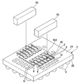
本発明の半導体モジュールについて説明する。図1は、本実施形態に係る半導体モジュール1を模式的に示す斜視図、図2は、断面図であって、図1のA−A線断面矢視図に相当する。また、図3は、本実施形態に係る半導体モジュール1の一部を拡大した平面図である。なお、以下の説明に用いる各図面では、各部材を認識可能な大きさとするため、各部材の縮尺を適宜変更している。
<Semiconductor module>
The semiconductor module of the present invention will be described. FIG. 1 is a perspective view schematically showing a
図1、図2及び図3において、半導体モジュール1は、インターポーザ2と、能動面3Aと裏面3Bとを有し、能動面3Aがインターポーザ2と対向するように配置された半導体チップ3と、半導体チップ3の裏面3Bと対向するように配置されたテープ基板40と、テープ基板40上又はインターポーザ2上に配置された受動部品4とを備えている。本発明の半導体モジュール1は、TAB(Tape Automated Bonding)技術を用いたパッケージである。
1, 2, and 3, a
インターポーザ2は、半導体チップ3の能動面3Aに対向する上面2Aと、その上面2Aとは反対側の下面2Bとを有している。
The
テープ基板40は、半導体チップ3の裏面3Bに対向する下面40B(第2の面)と、その下面40Bとは反対側の上面40A(第1の面)とを有している。
The
半導体チップ3は、インターポーザ2の上面2Aに実装され、その能動面3Aとインターポーザ2の上面2Aとが電気的に接続されている。また、半導体チップ3の裏面3Bとテープ基板40の下面40Bとは、例えば樹脂等の接着剤で接着されている。
The
インターポーザ2は、例えばエポキシ樹脂、ポリイミド樹脂等の合成樹脂(有機材料)、セラミックス、及びガラス等の絶縁性の材料によって形成された基板と、その基板に形成された導電性の配線パターンとを備えている。
The
テープ基板40は、例えばポリエステル樹脂、ポリイミド樹脂等の合成樹脂(有機材料)によって形成された絶縁性の薄膜フィルム41(図2参照)と、その上面40A側に形成された導電性の配線パターンとを備えている。この配線パターンは、複数の電極(端子)を含むCu配線からなる。
The
半導体チップ3は、シリコン基板を含み、トランジスタ、メモリ素子等を含む電子回路(集積回路)を有する。
The
受動部品4は、抵抗、コンデンサ、及びインダクタ等を含む。本実施形態においては、半導体モジュール1が複数の受動部品4を備えている。インターポーザ2及びテープ基板40に複数の受動部品が実装されている。
The
インターポーザ2の上面2Aには、端子5、12が形成されており、テープ基板40の上面40Aには、端子8(第1の端子)が形成されている。この端子8は、テープ基板40の上面40Aに形成された配線パターンの一部であって、配線パターンは、端子8、配線7によって構成される。
端子5、端子8及び端子12はそれぞれ電極パッド(ランド)であり、これら端子5,8、12の表面は例えば金(Au)によってメッキされている。以下の説明においては、端子5、8、12を適宜、電極パッド5,8,12と称する。
The
電極パッド8は、複数の受動部品4に対応するように、テープ基板40の上面40Aにおいて複数形成されている。図1及び図3において、受動部品4は、テープ基板40の上面40Aに6つ配置されており、電極パッド8は、1つの受動部品4に対して2つずつ、全部で12箇所に形成されている。そして、これらの電気パッド8に対応して、電気パッド5も12箇所に形成されている。この場合、電気パッド8は、テープ基板40の上面40Aの対向する二辺に沿って並ぶように形成されている。
A plurality of
薄膜フィルム41の側縁には、配線7とそれぞれ電気的に接続するアウタリード6(外延リード)が設けられている。このアウタリード6は、配線7に接続して、上面40Aから外延して形成されており、配線7との接続部、すなわち薄膜フィルム41の側縁において、インターポーザ2側にガルウィング状に折り曲げられている。
Outer leads 6 (extended leads) that are electrically connected to the
アウタリード6の先端には、端子42が形成され、端子42の下面には、不図示のバンプが形成されている。そして、このバンプを介して端子42と端子5が電気的に接続され、テープ基板40上の電極パッド8がインターポーザ2と電気的に接続されることになる。
端子8、配線7、外延リード6、端子42から構成される部材を、配線リード19と呼ぶ。
A
A member composed of the
なお、端子42も電極パッド(ランド)であり、端子42の表面は例えば金(Au)によってメッキされている。以下の説明においては、端子42を適宜、電極パッド42と称する。
The terminal 42 is also an electrode pad (land), and the surface of the terminal 42 is plated with, for example, gold (Au). In the following description, the terminal 42 is appropriately referred to as an
なお、図1において、アウタリード6は12本形成され、端子42は12個形成されている。また、アウタリード6は、Cu配線からなり、電気パッド42の下面に形成されたバンプは金及び無鉛はんだからなる。
In FIG. 1, twelve
本実施形態においては、図1,2において、テープ基板40は、半導体チップ3の裏面3Bに対して下面40B側を対向させた状態で貼り合わされている。半導体チップ3の裏面3Bとテープ基板40の下面40Bとは接着剤35によって接続されている。接着剤35としては、例えば樹脂等を用いることができる。
In this embodiment, in FIGS. 1 and 2, the
また、本実施形態では、インターポーザ2に対して、半導体チップ3がフリップチップ実装されている。半導体チップ3の能動面3Aには、金及び無鉛はんだの少なくとも一方を含むバンプ30が形成されている。また、インターポーザ2の上面2Aには、半導体チップ3のバンプ30と電気的に接続可能な接続端子21が形成されている。そして、半導体チップ3がインターポーザ2に対してフリップチップ実装されることによって、インターポーザ2の上面2Aと半導体チップ3の能動面3Aとが電気的に接続される。本実施形態では、フリップチップ実装において、バンプ30と接続端子21とを位置合わせし、荷重を加えつつ所定の方向に振動させ、その摩擦熱によってバンプ30と接続端子21とを機械的且つ電気的に接続する方法(超音波接合)が用いられる。
In the present embodiment, the
半導体チップ3をインターポーザ2上に実装する際の接合材としては、異方性導電フィルム(ACF:Anisotropic Conductive Film)、異方性導電ペースト(ACP:Anisotropic Conductive Paste)、非導電性フィルム(NCF:Non Conductive Film)、及び非導電性ペースト(NCP:Non Conductive Paste)の少なくとも一つを用いることができる。また、実装する際、加熱しつつ加圧するようにしてもよいし、超音波を作用させながら実装してもよい。なお、接合材を用いない場合には、半導体チップ3をインターポーザ2に実装した後、半導体チップ3とインターポーザ2との間にアンダーフィル材を充填してもよい。
As a bonding material for mounting the
また、半導体チップ3は、インターポーザ2の上面2Aの一部の領域2Cに実装されている。以下の説明において、インターポーザ2の上面2Aのうち、半導体チップ3が実装される領域2Cを適宜、実装領域2C、と称する。
Further, the
本実施形態においては、インターポーザ2の上面2Aのうち半導体チップ3が実装された実装領域2C以外の非実装領域2Dにも、受動部品4が実装されている。受動部品4は、インターポーザ2の上面2Aに形成された電極パッド12と電気的に接続される。本実施形態においては、受動部品4及びその受動部品4と接続される電極パッド12の少なくとも一部は、実装領域2Cに実装された半導体チップ3を囲むように複数設けられている。
In the present embodiment, the
また、インターポーザ2のうち、半導体チップ3が実装される上面2Aとは反対側の下面2Bには、例えばマザーボード等の外部機器と電気的に接続可能な端子13が形成されている。本実施形態においては、端子13は、はんだボールによって形成されている。
Further, in the
また、インターポーザ2の上面2A側に実装された半導体チップ3、当該半導体チップ3の裏面3B側に実装されたテープ基板40、当該テープ基板40上に実装された受動部品4等は、樹脂14(図2)によって覆われている。樹脂14は型(モールド)を形成する。図1においては、樹脂14は省略されている。
Further, the
なお、電極パッド5,8,12やアウタリード6の数は上記した数に特に限定されるものではなく、必要な数だけ適宜設けられる。
The number of
[半導体モジュールの製造方法]
次に、半導体モジュール1を製造する手順の一例について図4〜図9を用いて説明する。なお、本実施形態においては、既存の半導体チップ3を用いて半導体モジュール1を構成してもよいし、以下に説明するように半導体チップ3を始めから形成することとしてもよい。
[Method of manufacturing semiconductor module]
Next, an example of a procedure for manufacturing the
シリコン基板の第1面に集積回路等を形成し能動面3Aとし、その能動面3Aにバンプ30を形成した後、それを図5に示すようにダイシング(切断)して半導体チップ3を得る。
一方、インターポーザ2の上面2Aには接続端子21、及び電極パッド5、電極パッド12を形成する。
そして、図4(a)に示すように、インターポーザ2の実装領域2Cに、半導体チップ3を、その能動面3Aがインターポーザ2の上面2Aに対向するように配置する。そして、図4(b)に示すように、半導体チップ3をインターポーザ2上にフリップチップ実装する。この実装によって、半導体チップ3とインターポーザ2とが電気的に接続される。
An integrated circuit or the like is formed on the first surface of the silicon substrate to form an
On the other hand, the
Then, as shown in FIG. 4A, the
このフリップチップ実装には、金属圧着式、ろう材や異方性導電材を用いた加圧加熱式、超音波振動式(超音波加熱方式)などを用いることができる。本実施形態では、上述したように超音波接合(Au−Au接合)することにより、狭ピッチに対応した電気接続を可能としている。これは、半導体チップ3のバンプ30とインターポーザ2の接続端子21との接合に留まらず、能動面3Aと上面2Aとの接着性を向上させる手段としても有効である。
For the flip chip mounting, a metal crimping method, a pressure heating method using a brazing material or an anisotropic conductive material, an ultrasonic vibration method (ultrasonic heating method), or the like can be used. In the present embodiment, as described above, ultrasonic connection (Au—Au bonding) is performed to enable electrical connection corresponding to a narrow pitch. This is effective not only for bonding the
また、別の工程においてテープ基板40を形成する。なお、本実施形態においては、既存のテープ基板40を用いて半導体モジュール1を構成してもよいし、以下に説明するようにテープ基板40を始めから形成することとしてもよい。
Further, the
テープ基板40は、図6に示すように、ポリイミドテープなどに代表される薄膜フィルム41の絶縁基材に、Cuから成る配線リード19を載置して接着することで形成する。配線リード19の一部はアウタリード6として薄膜フィルム41から外延しており、配線リード19の両先端には、電極パッド8及び電極パッド42を形成されている。
As shown in FIG. 6, the
そして、図4(c)に示すように、このテープ基板40を、半導体チップ3の裏面3Bに、下面40Bを対向させた状態で、接着剤35によって張り合わせる。この接着剤35は、例えばインクジェット法、ディスペンス法、印刷法等を用いて、半導体チップ3の裏面3B及びテープ基板40の下面40Bの少なくとも一方に供給可能である。
Then, as shown in FIG. 4C, the
次に、図4(d)に示すように、インターポーザ2の電極パッド5とテープ基板40の電極パッド42とを電気的に接続する。
この電極パッド5と電極パッド42とを接続する方法としては、図7に示すような、一括ボンディング方式を採用することができる。これは、あらかじめ電極パッド42に不図示のバンプを形成しておき、12対の電極パッド5と電極パッド42をそれぞれ対向させた状態で、加圧圧着治具50によって一括して加圧を行う、Au−Au熱圧着方法である。
この電気的な接続によって、後工程でテープ基板40の電極パッド8に載置される受動部品4とインターポーザ2とが電気的に接続されることになる。
Next, as shown in FIG. 4D, the
As a method of connecting the
By this electrical connection, the
そして、図4(e)に示すように、テープ基板40の電極パッド8上及び、インターポーザ2の電極パッド12上に、受動部品4を載置してそれぞれ接続する。例えば、電極パッド8上の受動部品4は、図3に示すように配置することができる。
And as shown in FIG.4 (e), the
ここで、受動部品4と電極パッド8または電極パッド12とは、導電性材料を含む接着剤を介することによって、電気的に接続(ボンディング)される。この接着剤としては、例えば導電性樹脂、無鉛はんだ等を用いることができる。そして、この接着剤は、例えばインクジェット法、ディスペンス法、印刷法等を用いて、受動部品4及びインターポーザ2の電極パッド8の少なくとも一方に供給可能である。
Here, the
最後に、図4(e)に示すように、インターポーザ2の上面2A側に実装された半導体チップ3、テープ基板40、受動部品4、アウタリード6等を覆うように、モールドを形成するための樹脂14を供給する。
Finally, as shown in FIG. 4E, a resin for forming a mold so as to cover the
また、インターポーザ2のうち、半導体チップ3が実装される上面2Aとは反対側の下面2Bに、例えばマザーボード等の外部機器と電気的に接続可能なはんだボール等の端子13を形成する。
Further, in the
以上説明したように、本実施形態によれば、インターポーザ2に、能動面3Aを対向させて半導体チップ3を実装するとともに、半導体チップ3の裏面3Bと対向するように受動部品4が接続されたテープ基板40を配置するようにしたので、半導体モジュール1の小型化、特にインターポーザ2の表面(上面2A、下面2B)、及びテープ基板40の表面(上面40A、下面40B)と平行な面内における半導体モジュール1の小型化を実現することができる。
As described above, according to the present embodiment, the
すなわち、受動部品4を有する半導体モジュール1において、全ての受動部品4を、例えばインターポーザ2の上面2Aに設け、インターポーザ2上に半導体チップ3と受動部品4とを並べるように配置する場合、受動部品4を配置するための領域を確保しなければならず、半導体モジュール1の小型化、特に、インターポーザ2の上面2Aと平行な面内における半導体モジュール1の小型化が困難となる。
That is, in the
本実施形態においては、図2に示すように、半導体モジュール1に実装される受動部品4の少なくとも一部を、半導体チップ3を介してテープ基板40上に実装するようにしたので、半導体モジュール1の小型化を実現することができる。
In the present embodiment, as shown in FIG. 2, at least a part of the
また、本実施形態においては、半導体モジュール1を製造する際、インターポーザ2とテープ基板40とを電気的に接続した後、すなわち、インターポーザ2の電極パッド5に対してテープ基板40の配線リード19を接続した後に、インターポーザ2に受動部品4を実装するようにしたので、インターポーザ2上の受動部品4が加圧圧着治具50による接続の妨げになることを避けることができる。これにより、半導体モジュール1を製造する際の工程の複雑化等を抑制できる。
In the present embodiment, when the
また、本実施形態の配線リード19は、その先端に電極パッド42を備えたバンプ付のリードであることから、治具による加圧によって断線することもなく、電極パッド5との電気的接続を良好にすることができる。
In addition, since the
また、本実施形態においては、半導体チップ3上に、受動部品4とインターポーザ2とを電気的に接続する配線パターンを有したテープ基板40を備えたことから、半導体チップ3側の裏面3Bに配線パターンを形成する必要がなく、各部材を組み立てるだけでよいことになる。これにより、製造工程が簡略化され、半導体モジュール1を製造する際の工程の複雑化等を抑制できる。
In the present embodiment, since the
また、テープ基板40を用いることで、半導体モジュール1の高さ方向における小型化、すなわち薄型化を実現することができる。
Further, by using the
<他の製造方法>
本発明の半導体モジュールの製造方法の他の実施形態について図8及び図9を用いて説明する。
上述の実施形態においては、インターポーザ2に半導体チップ3を先に実装し、その後半導体チップ3上にテープ基板40を実装するようにしたが、他の実施形態においては、半導体チップ3とテープ基板40とを先に貼り合わせ、その後、テープ基板40を備えた半導体チップ3をインターポーザ2に実装するようにしてもよい。
<Other manufacturing methods>
Another embodiment of the semiconductor module manufacturing method of the present invention will be described with reference to FIGS.
In the above-described embodiment, the
例えば、図8に示すように、テープ基板40上を下面40B側を上にした状態で、半導体チップ3を裏面3Bを下面40Bに対向させて配置し、半導体チップ3とテープ基板40とを貼り合わせる。その後、一体となされた半導体チップ3とテープ基板40とを裏返して、図4(c)に示すように、インターポーザ2の上面2Aに対向させる。この後の工程は、先に述べた製造方法と同様である。
For example, as shown in FIG. 8, the
以上、添付図面を参照しながら本発明に係る好適な実施形態について説明したが、本発明は係る例に限定されないことは言うまでもなく、上記各実施形態を組み合わせても良い。当業者であれば、特許請求の範囲に記載された技術的思想の範疇内において、各種の変更例または修正例に想到し得ることは明らかであり、それらについても当然に本発明の技術的範囲に属するものと了解される。 The preferred embodiments according to the present invention have been described above with reference to the accompanying drawings. However, it goes without saying that the present invention is not limited to such examples, and the above embodiments may be combined. It is obvious for those skilled in the art that various changes or modifications can be conceived within the scope of the technical idea described in the claims. It is understood that it belongs to.
例えば、上述の実施形態においては、インターポーザ2の上面2Aに、受動部品4を接続可能な領域2Dを設けているが、所定数の受動部品4の全てをテープ基板40の上面40Aに接続可能であるならば、領域2Dは無くてもよい。こうすることにより、より一層、半導体モジュール1を小型化することができる。
For example, in the above-described embodiment, the
また、上述の実施形態においては、インターポーザ2上に受動部品4を実装する工程と、テープ基板40上に受動部品4を実装する工程とを同時に行うこととしたが、電極パッド42を電極パッド5に接続する前に、テープ基板上の受動部品のみ実装しても良い。
In the above embodiment, the step of mounting the
また、上述の実施形態においては、電極パッド42にバンプを備える構成としたが、インターポーザ2の電極パッド5上にバンプを設けるようにしてもよい。
In the above-described embodiment, the
1…半導体モジュール、2…インターポーザ、2A…上面、3…半導体チップ、3A…能動面、3B…裏面、4…受動部品、5,8,12…電極パッド(端子)、7…配線、6…アウタリード(外延リード)、10…接続端子、19…配線リード、2C…実装領域、2D…領域、40…テープ基板、40A…上面、40B…下面、42…電極パッド(端子)
DESCRIPTION OF
Claims (5)
能動面と裏面とを有し、前記能動面が前記インターポーザと対向して配置された半導体チップと、
第1の面に配線パターンを有し、前記第1の面とは反対側の第2の面を前記半導体チップの前記裏面に対向して配置されたテープ基板と、
前記テープ基板の前記第1の面に実装されて前記配線パターンに電気的に接続された複数の受動部品と、を備え、
前記テープ基板は、前記配線パターンに接続する複数の外延リードを有し、当該外延リードを介して前記配線パターンが前記インターポーザに電気的に接続されていることを特徴とする半導体モジュール。 With an interposer,
A semiconductor chip having an active surface and a back surface, wherein the active surface is disposed to face the interposer;
A tape substrate having a wiring pattern on the first surface, and a second surface opposite to the first surface disposed opposite the back surface of the semiconductor chip;
A plurality of passive components mounted on the first surface of the tape substrate and electrically connected to the wiring pattern,
The tape substrate has a plurality of external leads connected to the wiring pattern, and the wiring pattern is electrically connected to the interposer via the external leads.
インターポーザに、前記能動面が前記インターポーザと対向するようにして前記半導体チップを実装する工程と、
前記半導体チップの前記裏面に、前記第1の面とは反対側の第2の面を対向させて前記テープ基板を貼り合わせる工程と、
前記テープ基板の前記第1の面上に受動部品を実装する工程と、
前記インターポーザと前記配線パターンとを、前記外延リードを介して電気的に接続する工程と、を含むことを特徴とする半導体モジュールの製造方法。 Preparing a semiconductor chip having an active surface and a back surface, a tape substrate having a wiring pattern formed on the first surface side and an extending lead connected to the wiring pattern;
Mounting the semiconductor chip on an interposer so that the active surface faces the interposer;
Bonding the tape substrate to the back surface of the semiconductor chip with the second surface opposite to the first surface facing the second surface;
Mounting passive components on the first surface of the tape substrate;
And a step of electrically connecting the interposer and the wiring pattern via the extension leads.
Priority Applications (1)
| Application Number | Priority Date | Filing Date | Title |
|---|---|---|---|
| JP2007156303A JP2008311347A (en) | 2007-06-13 | 2007-06-13 | Semiconductor module and its manufacturing method |
Applications Claiming Priority (1)
| Application Number | Priority Date | Filing Date | Title |
|---|---|---|---|
| JP2007156303A JP2008311347A (en) | 2007-06-13 | 2007-06-13 | Semiconductor module and its manufacturing method |
Publications (2)
| Publication Number | Publication Date |
|---|---|
| JP2008311347A true JP2008311347A (en) | 2008-12-25 |
| JP2008311347A5 JP2008311347A5 (en) | 2010-07-22 |
Family
ID=40238719
Family Applications (1)
| Application Number | Title | Priority Date | Filing Date |
|---|---|---|---|
| JP2007156303A Withdrawn JP2008311347A (en) | 2007-06-13 | 2007-06-13 | Semiconductor module and its manufacturing method |
Country Status (1)
| Country | Link |
|---|---|
| JP (1) | JP2008311347A (en) |
Cited By (2)
| Publication number | Priority date | Publication date | Assignee | Title |
|---|---|---|---|---|
| JP2012129555A (en) * | 2009-01-20 | 2012-07-05 | Altera Corp | Ic package having capacitors arranged on insertion layer |
| US9160048B2 (en) | 2012-06-04 | 2015-10-13 | Fujitsu Limited | Electronic device with terminal circuits |
-
2007
- 2007-06-13 JP JP2007156303A patent/JP2008311347A/en not_active Withdrawn
Cited By (3)
| Publication number | Priority date | Publication date | Assignee | Title |
|---|---|---|---|---|
| JP2012129555A (en) * | 2009-01-20 | 2012-07-05 | Altera Corp | Ic package having capacitors arranged on insertion layer |
| JP2012518893A (en) * | 2009-01-20 | 2012-08-16 | アルテラ コーポレイション | IC package having a capacitor disposed on an insertion layer |
| US9160048B2 (en) | 2012-06-04 | 2015-10-13 | Fujitsu Limited | Electronic device with terminal circuits |
Similar Documents
| Publication | Publication Date | Title |
|---|---|---|
| US8786102B2 (en) | Semiconductor device and method of manufacturing the same | |
| US8432033B2 (en) | Electronic device and manufacturing method therefor | |
| US7679178B2 (en) | Semiconductor package on which a semiconductor device can be stacked and fabrication method thereof | |
| JP2008166439A (en) | Semiconductor device and manufacturing method thereof | |
| US6521483B1 (en) | Semiconductor device, method of manufacture thereof, circuit board, and electronic device | |
| KR20060101385A (en) | A semiconductor device and a manufacturing method of the same | |
| JP2007267113A (en) | Piezoelectric device and manufacturing method therefor | |
| TW579560B (en) | Semiconductor device and its manufacturing method | |
| JP4965989B2 (en) | Electronic component built-in substrate and method for manufacturing electronic component built-in substrate | |
| JP2001077294A (en) | Semiconductor device | |
| US6410366B1 (en) | Semiconductor device and manufacturing method thereof, circuit board and electronic equipment | |
| JP2000269407A (en) | Electronic module and electronic apparatus | |
| JP2008218758A (en) | Electronic circuit mounting structure | |
| US20100032802A1 (en) | Assembling of Electronic Members on IC Chip | |
| JP3847602B2 (en) | Stacked semiconductor device, method for manufacturing the same, motherboard mounted with semiconductor device, and method for manufacturing motherboard mounted with semiconductor device | |
| JP2008311347A (en) | Semiconductor module and its manufacturing method | |
| JP3332555B2 (en) | Semiconductor device and manufacturing method thereof | |
| JP4417974B2 (en) | Manufacturing method of stacked semiconductor device | |
| US8975758B2 (en) | Semiconductor package having interposer with openings containing conductive layer | |
| JP2003249606A (en) | Semiconductor device and interposer | |
| WO2001033623A1 (en) | Semiconductor device and its manufacturing method | |
| JP3879803B2 (en) | Semiconductor device and manufacturing method thereof, circuit board, and electronic apparatus | |
| JP2008021842A (en) | Semiconductor module, and manufacturing method of semiconductor module | |
| JP2003133509A (en) | Semiconductor package and method for manufacturing the same | |
| JP2008306037A (en) | Semiconductor module and method for manufacturing the same |
Legal Events
| Date | Code | Title | Description |
|---|---|---|---|
| A521 | Request for written amendment filed |
Free format text: JAPANESE INTERMEDIATE CODE: A523 Effective date: 20100603 |
|
| A621 | Written request for application examination |
Free format text: JAPANESE INTERMEDIATE CODE: A621 Effective date: 20100603 |
|
| A521 | Request for written amendment filed |
Free format text: JAPANESE INTERMEDIATE CODE: A821 Effective date: 20100604 |
|
| A761 | Written withdrawal of application |
Free format text: JAPANESE INTERMEDIATE CODE: A761 Effective date: 20110314 |
|
| A521 | Request for written amendment filed |
Free format text: JAPANESE INTERMEDIATE CODE: A821 Effective date: 20110315 |