JP2008257525A - Power unit - Google Patents
Power unit Download PDFInfo
- Publication number
- JP2008257525A JP2008257525A JP2007099811A JP2007099811A JP2008257525A JP 2008257525 A JP2008257525 A JP 2008257525A JP 2007099811 A JP2007099811 A JP 2007099811A JP 2007099811 A JP2007099811 A JP 2007099811A JP 2008257525 A JP2008257525 A JP 2008257525A
- Authority
- JP
- Japan
- Prior art keywords
- power supply
- circuit
- output voltage
- voltage
- switching
- Prior art date
- Legal status (The legal status is an assumption and is not a legal conclusion. Google has not performed a legal analysis and makes no representation as to the accuracy of the status listed.)
- Pending
Links
Images

Abstract
Description
本発明は、スイッチング電源回路とシリーズ電源回路とを備える電源装置に関するものである。 The present invention relates to a power supply device including a switching power supply circuit and a series power supply circuit.
シリーズ電源回路は、出力電圧に応じた電圧値を検出して、この検出電圧と所定の基準電圧とを比較する。その比較結果に応じて、制御トランジスタのオン状態における導通状態、すなわち、コレクタ・エミッタ間の電圧の大きさを制御する。具体的には、検出電圧が基準電圧よりも高ければコレクタ・エミッタ間電圧を高め、逆に低ければコレクタ・エミッタ間電圧を低下させる。これにより出力電圧が安定化するので、シリーズ電源回路は、入力電圧から目標とする出力電圧を高精度に発生することができる。 The series power supply circuit detects a voltage value corresponding to the output voltage, and compares this detected voltage with a predetermined reference voltage. According to the comparison result, the conduction state in the ON state of the control transistor, that is, the magnitude of the voltage between the collector and the emitter is controlled. Specifically, when the detection voltage is higher than the reference voltage, the collector-emitter voltage is increased, and conversely, when the detection voltage is lower, the collector-emitter voltage is decreased. As a result, the output voltage is stabilized, so that the series power supply circuit can generate the target output voltage from the input voltage with high accuracy.
しかしながら、シリーズ電源回路では、入力電圧を電圧降下させることによって出力電圧を発生させているので、必然的に比較的大きな電力損失が発生してしまう。この電力損失は入力電圧と出力電圧の差が大きいほど大きくなる。 However, in the series power supply circuit, since the output voltage is generated by dropping the input voltage, a relatively large power loss inevitably occurs. This power loss increases as the difference between the input voltage and the output voltage increases.
一方、電力損失を低減可能な電源回路としてスイッチング電源回路が知られている。このスイッチング電源回路では、入力電圧をスイッチング素子のオンオフ動作によって断続させ、コイルとコンデンサとによって平滑化する。このように、スイッチング電源回路は、スイッチング素子のオンオフ動作によって出力電圧の調整を行なうので、電力損失を低減することができる。 On the other hand, a switching power supply circuit is known as a power supply circuit capable of reducing power loss. In this switching power supply circuit, the input voltage is intermittently turned on and off by the switching element, and smoothed by the coil and the capacitor. Thus, since the switching power supply circuit adjusts the output voltage by the on / off operation of the switching element, it is possible to reduce power loss.
しかしながら、スイッチング電源回路では、スイッチング素子のオンオフ動作に伴って、リップル電圧等のノイズが発生してしまう。 However, in the switching power supply circuit, noise such as ripple voltage is generated with the on / off operation of the switching element.
このため、例えば特許文献1に開示されるように、スイッチング電源回路とシリーズ電源回路とを直列に接続した電源装置が提案されている。この電源装置によれば、入力電圧は、スイッチング電源回路で予め電圧降下された後にシリーズ電源回路に与えられるので、電力損失の低減を図ることができるとともに、スイッチング電源回路によるノイズはシリーズ電源回路によって平滑化されるため、ノイズの抑制も図ることができる。
シリーズ電源回路の制御トランジスタに入力される電圧が高いほど、そこで発生する電力損失が大きくなるとともに、発生する熱量が大きくなる。従って、何らかの原因で前段のスイッチング電源回路がオン状態で故障してしまうと、シリーズ電源回路の制御トランジスタにおいて発生する熱量が大きくなる。そのため、スイッチング電源回路がオン状態で故障してしまうと、シリーズ電源回路の制御トランジスタが熱破壊する恐れがある。 The higher the voltage input to the control transistor of the series power supply circuit, the greater the power loss generated there and the greater the amount of heat generated. Therefore, if the switching power supply circuit in the previous stage breaks down for some reason, the amount of heat generated in the control transistor of the series power supply circuit increases. Therefore, if the switching power supply circuit fails in the on state, the control transistor of the series power supply circuit may be thermally destroyed.
本発明は、この事情に基づいて成されたものであり、その目的とするところは、スイッチング電源回路とシリーズ電源回路とを備えた電源装置において、シリーズ電源回路の制御トランジスタの熱破壊を防止することにある。 The present invention has been made based on this situation, and an object thereof is to prevent thermal destruction of a control transistor of a series power supply circuit in a power supply apparatus including a switching power supply circuit and a series power supply circuit. There is.
その目的を達成するための請求項1記載の発明は、スイッチング素子のオンオフ状態をスイッチング制御回路によって制御することで、入力電圧を当該入力電圧よりも低い中間出力電圧に変換して出力するスイッチング電源回路と、制御トランジスタを備え、当該制御トランジスタのオン状態における導通状態を調節することによって、前記中間出力電圧を所定の目標出力電圧まで電圧降下させて出力するシリーズ電源回路とを備えた電源装置であって、前記シリーズ電源回路は、前記中間出力電圧が予め設定された入力上限電圧以上であるか否かを判定することによって、前記中間出力電圧が過電圧であるか否かを判定する過電圧判定部を備え、その過電圧判定部によって過電圧であると判定された場合には前記制御トランジスタをオフにすることを特徴とする。 In order to achieve the object, the invention according to claim 1 is a switching power supply that converts an input voltage to an intermediate output voltage lower than the input voltage and outputs it by controlling an on / off state of the switching element by a switching control circuit. A power supply apparatus comprising a circuit and a series power supply circuit that includes a control transistor and outputs the intermediate output voltage by dropping the intermediate output voltage to a predetermined target output voltage by adjusting a conduction state in an ON state of the control transistor. The series power supply circuit determines whether or not the intermediate output voltage is an overvoltage by determining whether or not the intermediate output voltage is equal to or higher than a preset input upper limit voltage. And when the overvoltage determination unit determines that the overvoltage is present, the control transistor is turned off. And wherein the Rukoto.
スイッチング電源回路がオン状態で故障すると、スイッチング電源回路から出力される中間出力電圧が高くなる。この場合、請求項1の発明では、過電圧検出部によって中間出力電圧が過電圧であると判定されて、制御トランジスタがオフされる。従って、制御トランジスタの熱破壊が防止できる。 When the switching power supply circuit fails in the on state, the intermediate output voltage output from the switching power supply circuit increases. In this case, according to the first aspect of the present invention, the overvoltage detector determines that the intermediate output voltage is an overvoltage, and the control transistor is turned off. Therefore, thermal destruction of the control transistor can be prevented.
以下、本発明の電源装置の実施の形態を図面に基づいて説明する。図1は、本発明が適用された電源装置10全体の概略構成を示す図である。 Embodiments of a power supply apparatus according to the present invention will be described below with reference to the drawings. FIG. 1 is a diagram showing a schematic configuration of an entire power supply apparatus 10 to which the present invention is applied.
図1において、入力端子12は、図示しない車載バッテリに接続されており、その車載バッテリから入力電圧Vinの信号が入力される。この入力端子12は、その下流側にノーマリオン型のMOSFETからなるスイッチング素子14が接続されている。このスイッチング素子14は、後述するスイッチング制御回路30から与えられる駆動パルス信号SPによってオンオフ動作する。
In FIG. 1, the
スイッチング素子14の下流には、スイッチング素子14から断続して出力される電圧を平滑化するために、平滑回路20が接続されている。平滑回路20は、スイッチング素子14の出力側(ソース)に接続されたチョークコイル22と、このチョークコイル22の両端とグランド側との間に接続されたフリーホイールダイオード24およびコンデンサ26とから構成される。
A
平滑回路20の出力は、スイッチング制御回路30に入力される。このスイッチング制御回路30は、スイッチング素子14のオンオフ状態を制御するものであり、スイッチング素子14、平滑回路20、およびこのスイッチング制御回路30によって、スイッチング電源回路16が構成される。
The output of the
スイッチング制御回路30は、抵抗直列回路31および基準電源回路32を備えている。抵抗直列回路31は、抵抗R1および抵抗R2が直列接続されたものであり、入力された電圧に応じた帰還電圧Vf1を生成する。基準電源回路32は、平滑回路20の出力電圧の基準となる第1基準電圧Vref1を発生させる。
The
基準電源回路32にて発生する第1基準電圧Vref1および抵抗直列回路31によって生成された帰還電圧Vf1はエラーアンプ33に入力される。エラーアンプ33は入力された第1基準電圧Vref1と帰還電圧Vf1との差を増幅して出力する。
The first reference voltage Vref1 generated in the reference
スイッチング制御回路30は、さらに、スイッチング素子14をオンオフ動作させるための駆動パルス信号SPを生成するPWM(Pulse Width Modulation)回路34を備えている。エラーアンプ33からの増幅出力と三角波発生回路35で発生した三角波とがこのPWM回路34に入力される。PWM回路34は、エラーアンプ33の増幅出力と三角波発生回路35で発生した三角波とを比較し、三角波が増幅出力を上回っている期間にLoレベルの信号を発生し、下回っている期間にHiレベルの信号を発生することによって、スイッチング素子14を駆動するための駆動パルス信号SPを生成する。
The
なお、本実施形態のスイッチング素子14はノーマリオン型のMOSFETからなるため、PWM回路34からLoレベルの信号が出力されたときにオンし、Hiレベルの信号が出力されたときにオフする。駆動回路36は、PWM回路34から出力された駆動パルス信号SPを、スイッチング素子14を駆動できるレベルまで増幅する回路である。
Since the switching element 14 of the present embodiment is formed of a normally-on type MOSFET, it is turned on when a Lo level signal is output from the
スイッチング素子14がオン・オフされることによって入力電圧Vinの信号はPWM変調される。そして、PWM変調された信号が平滑回路20で平滑化されることによって、後述するシリーズ電源回路40の目標出力電圧に近い所定の中間出力電圧Vout1の信号となる。この中間出力電圧Vout1は、抵抗R1、R2の値および基準電源回路32にて発生させる第1基準電圧Vref1を調整することによって調整可能であり、たとえば、目標出力電圧を5Vとすると、中間出力電圧Vout1は6.5Vに設定される。
When the switching element 14 is turned on / off, the signal of the input voltage Vin is PWM-modulated. Then, the PWM modulated signal is smoothed by the
上記構成のスイッチング電源回路16にシリーズ電源回路40が直列に接続されている。このシリーズ電源回路40は、PNP型である制御トランジスタ42、およびコントロール回路44を備えている。
A series power supply circuit 40 is connected in series to the switching power supply circuit 16 having the above configuration. The series power supply circuit 40 includes a
コントロール回路44には中間出力電圧Vout1が入力される。また、制御トランジスタ42の出力電圧Vout2は、出力端子48に出力されるとともに、コントロール回路44にも入力される。
The
コントロール回路44は、出力電圧Vout2に応じて制御トランジスタ42のベース電流を制御することで、その出力電圧Vout2を目標出力電圧(5V)に制御する。ただし、中間出力電圧Vout1が予め設定された入力上限電圧以上である場合には制御トランジスタ42をオフにする。
The
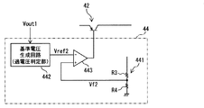
図2は、上記コントロール回路44の具体的回路構成例を示す図である。図2に示すコントロール回路44は、抵抗直列回路441、基準電圧生成回路442、エラーアンプ443を備えている。
FIG. 2 is a diagram showing a specific circuit configuration example of the
抵抗直列回路441は、抵抗R3および抵抗R4が直列接続されたものであり、抵抗R3の一方の端(抵抗R4側とは反対側の端)の電位は出力電圧Vout2である。この抵抗直列回路441は、出力電圧Vout2を分圧して帰還電圧Vf2を生成する。
The
基準電圧生成回路442は所定の第2基準電圧Vref2を発生させる。ただし、この基準電圧生成回路442は過電圧判定部としても機能しており、中間出力電圧Vout1が予め設定された入力上限電圧以上である場合には、中間出力電圧Vout1が過電圧であると判定する。そして、制御トランジスタ42をオフにするために、第2基準電圧Vref2を0Vにする。なお、入力上限電圧は、正常時の中間出力電圧Vout1の変動範囲の上限値よりも大きい値であって、入力電圧Vinよりも低い値に設定されている。
The reference
エラーアンプ443は、第2基準電圧Vref2と帰還電圧Vf2の差を増幅して出力する。この出力は制御トランジスタ42のベースに入力される。このように構成されていることにより、エラーアンプ443の出力によって制御トランジスタ42のベース電流が制御され、また、制御トランジスタ42の出力電圧Vout2は式1に示す値となる。
(式1) Vout2=Vref2・(R3+R4)/R4
上記式1からも分かるように、第2基準電圧Vref2が0Vのときは、出力電圧Vout2は0V、すなわち制御トランジスタ42はオフとなる。
The
(Expression 1) Vout2 = Vref2 · (R3 + R4) / R4
As can be seen from the above equation 1, when the second reference voltage Vref2 is 0V, the output voltage Vout2 is 0V, that is, the
以上、説明したように本実施形態の電源装置10によれば、仮に、スイッチング電源回路16がオン状態で故障し、スイッチング電源回路16から出力される中間出力電圧Vout1が高くなったとしても、基準電圧生成回路442にて中間出力電圧Vout1が過電圧であると判定されて、制御トランジスタ42がオフされる。従って、制御トランジスタ42の熱破壊が防止できる。
As described above, according to the power supply device 10 of the present embodiment, even if the switching power supply circuit 16 fails in the ON state and the intermediate output voltage Vout1 output from the switching power supply circuit 16 becomes high, the reference The
以上、本発明の実施形態を説明したが、本発明は上述の実施形態に限定されるものではなく、本発明の要旨を逸脱しない範囲内で種々変更して実施することができる。 Although the embodiments of the present invention have been described above, the present invention is not limited to the above-described embodiments, and various modifications can be made without departing from the scope of the present invention.
10:電源装置
14:スイッチング素子
16:スイッチング電源回路
30:スイッチング制御回路
40:シリーズ電源回路
42:制御トランジスタ
44:コントロール回路
441:抵抗直列回路
442:基準電圧生成回路(過電圧生成回路)
443:エラーアンプ
10: power supply device 14: switching element 16: switching power supply circuit 30: switching control circuit 40: series power supply circuit 42: control transistor 44: control circuit 441: resistor series circuit 442: reference voltage generating circuit (overvoltage generating circuit)
443: Error amplifier
Claims (1)
制御トランジスタを備え、当該制御トランジスタのオン状態における導通状態を調節することによって、前記中間出力電圧を所定の目標出力電圧まで電圧降下させて出力するシリーズ電源回路とを備えた電源装置であって、
前記シリーズ電源回路は、前記中間出力電圧が予め設定された入力上限電圧以上であるか否かを判定することによって、前記中間出力電圧が過電圧であるか否かを判定する過電圧判定部を備え、その過電圧判定部によって過電圧であると判定された場合には前記制御トランジスタをオフにすることを特徴とする電源装置。 A switching power supply circuit that converts the input voltage to an intermediate output voltage lower than the input voltage by controlling the on / off state of the switching element by the switching control circuit, and
A power supply device comprising a series power supply circuit that includes a control transistor and outputs the intermediate output voltage by dropping the intermediate output voltage to a predetermined target output voltage by adjusting a conduction state in an ON state of the control transistor;
The series power supply circuit includes an overvoltage determination unit that determines whether the intermediate output voltage is an overvoltage by determining whether the intermediate output voltage is equal to or higher than a preset input upper limit voltage, The power supply device, wherein the control transistor is turned off when the overvoltage determination unit determines that the voltage is overvoltage.
Priority Applications (1)
| Application Number | Priority Date | Filing Date | Title |
|---|---|---|---|
| JP2007099811A JP2008257525A (en) | 2007-04-05 | 2007-04-05 | Power unit |
Applications Claiming Priority (1)
| Application Number | Priority Date | Filing Date | Title |
|---|---|---|---|
| JP2007099811A JP2008257525A (en) | 2007-04-05 | 2007-04-05 | Power unit |
Publications (1)
| Publication Number | Publication Date |
|---|---|
| JP2008257525A true JP2008257525A (en) | 2008-10-23 |
Family
ID=39981027
Family Applications (1)
| Application Number | Title | Priority Date | Filing Date |
|---|---|---|---|
| JP2007099811A Pending JP2008257525A (en) | 2007-04-05 | 2007-04-05 | Power unit |
Country Status (1)
| Country | Link |
|---|---|
| JP (1) | JP2008257525A (en) |
Cited By (3)
| Publication number | Priority date | Publication date | Assignee | Title |
|---|---|---|---|---|
| JP2012039752A (en) * | 2010-08-06 | 2012-02-23 | Ihi Corp | Drive circuit of semiconductor element |
| JP2012085507A (en) * | 2010-09-17 | 2012-04-26 | Toshiba Lighting & Technology Corp | Switching power supply and adjustable power supply system |
| JP2020061827A (en) * | 2018-10-05 | 2020-04-16 | 株式会社デンソー | Electronic control device |
Citations (6)
| Publication number | Priority date | Publication date | Assignee | Title |
|---|---|---|---|---|
| JPH03175513A (en) * | 1989-12-04 | 1991-07-30 | Sharp Corp | Stabilized power supply device |
| JPH10232721A (en) * | 1997-02-20 | 1998-09-02 | Sharp Corp | Output controller for dc stabilized power source and dc stabilized power source |
| JP2000139023A (en) * | 1998-11-04 | 2000-05-16 | Denso Corp | Onboard power supply |
| JP2000305639A (en) * | 1999-04-23 | 2000-11-02 | Sony Corp | Constant voltage regulator circuit |
| JP2004147437A (en) * | 2002-10-24 | 2004-05-20 | Denso Corp | Multi-output power supply device and in-vehicle electronic control device |
| JP2004147391A (en) * | 2002-10-22 | 2004-05-20 | Denso Corp | Power controller |
-
2007
- 2007-04-05 JP JP2007099811A patent/JP2008257525A/en active Pending
Patent Citations (6)
| Publication number | Priority date | Publication date | Assignee | Title |
|---|---|---|---|---|
| JPH03175513A (en) * | 1989-12-04 | 1991-07-30 | Sharp Corp | Stabilized power supply device |
| JPH10232721A (en) * | 1997-02-20 | 1998-09-02 | Sharp Corp | Output controller for dc stabilized power source and dc stabilized power source |
| JP2000139023A (en) * | 1998-11-04 | 2000-05-16 | Denso Corp | Onboard power supply |
| JP2000305639A (en) * | 1999-04-23 | 2000-11-02 | Sony Corp | Constant voltage regulator circuit |
| JP2004147391A (en) * | 2002-10-22 | 2004-05-20 | Denso Corp | Power controller |
| JP2004147437A (en) * | 2002-10-24 | 2004-05-20 | Denso Corp | Multi-output power supply device and in-vehicle electronic control device |
Cited By (4)
| Publication number | Priority date | Publication date | Assignee | Title |
|---|---|---|---|---|
| JP2012039752A (en) * | 2010-08-06 | 2012-02-23 | Ihi Corp | Drive circuit of semiconductor element |
| JP2012085507A (en) * | 2010-09-17 | 2012-04-26 | Toshiba Lighting & Technology Corp | Switching power supply and adjustable power supply system |
| JP2020061827A (en) * | 2018-10-05 | 2020-04-16 | 株式会社デンソー | Electronic control device |
| JP7063223B2 (en) | 2018-10-05 | 2022-05-09 | 株式会社デンソー | Electronic control device |
Similar Documents
| Publication | Publication Date | Title |
|---|---|---|
| JP4912067B2 (en) | Semiconductor integrated circuit and electronic device having the same | |
| JP3574394B2 (en) | Switching power supply | |
| JP3691500B2 (en) | Switching power supply | |
| JP4985003B2 (en) | DC-DC converter | |
| JP5050715B2 (en) | Light emitting diode drive circuit | |
| JP2007006651A (en) | Switching control circuit and self-excited dc-dc converter | |
| JP2007258227A (en) | Led drive circuit | |
| JP2011103725A (en) | Power factor improvement type switching power supply device | |
| JP2010051053A (en) | Control circuit for boost dc-dc converters and boost dc-dc converter | |
| WO2018043228A1 (en) | Switching power supply device and semiconductor device | |
| JP6932056B2 (en) | Switching regulator | |
| JP4969204B2 (en) | Overcurrent protection circuit | |
| JP2008257525A (en) | Power unit | |
| US20090200998A1 (en) | Buck switching regulator with improved mode transition and control method thereof | |
| US20140097811A1 (en) | Current-limit system and method | |
| JP2007097286A (en) | Switching regulator and its drive method | |
| JP4745711B2 (en) | Switching regulator | |
| JP5476141B2 (en) | Switching power supply circuit | |
| JP2008011585A (en) | Switching regulator | |
| JP5032447B2 (en) | Switching power supply | |
| JP2008271758A (en) | Dc-dc converter | |
| JP4423648B2 (en) | Discharge lamp lighting device | |
| JP2018082574A (en) | Switching power supply device | |
| JP4096621B2 (en) | Switching power supply | |
| JP2006129643A (en) | Switching control unit and semiconductor integrated circuit device |
Legal Events
| Date | Code | Title | Description |
|---|---|---|---|
| A621 | Written request for application examination |
Free format text: JAPANESE INTERMEDIATE CODE: A621 Effective date: 20090526 |
|
| A977 | Report on retrieval |
Effective date: 20110817 Free format text: JAPANESE INTERMEDIATE CODE: A971007 |
|
| A131 | Notification of reasons for refusal |
Effective date: 20110823 Free format text: JAPANESE INTERMEDIATE CODE: A131 |
|
| A02 | Decision of refusal |
Effective date: 20120110 Free format text: JAPANESE INTERMEDIATE CODE: A02 |