JP2008235010A - Method of manufacturing display device - Google Patents
Method of manufacturing display device Download PDFInfo
- Publication number
- JP2008235010A JP2008235010A JP2007072965A JP2007072965A JP2008235010A JP 2008235010 A JP2008235010 A JP 2008235010A JP 2007072965 A JP2007072965 A JP 2007072965A JP 2007072965 A JP2007072965 A JP 2007072965A JP 2008235010 A JP2008235010 A JP 2008235010A
- Authority
- JP
- Japan
- Prior art keywords
- transfer layer
- substrate
- display device
- layer
- manufacturing
- Prior art date
- Legal status (The legal status is an assumption and is not a legal conclusion. Google has not performed a legal analysis and makes no representation as to the accuracy of the status listed.)
- Pending
Links
- 238000004519 manufacturing process Methods 0.000 title claims abstract description 50
- 239000000758 substrate Substances 0.000 claims abstract description 181
- 238000000034 method Methods 0.000 claims abstract description 92
- 239000000463 material Substances 0.000 claims abstract description 83
- 230000008569 process Effects 0.000 claims abstract description 34
- 238000010438 heat treatment Methods 0.000 claims description 51
- 238000000576 coating method Methods 0.000 claims description 27
- 230000001681 protective effect Effects 0.000 claims description 25
- 239000011248 coating agent Substances 0.000 claims description 24
- 238000006243 chemical reaction Methods 0.000 claims description 22
- 230000008018 melting Effects 0.000 claims description 21
- 238000002844 melting Methods 0.000 claims description 21
- 230000009477 glass transition Effects 0.000 claims description 20
- 239000011368 organic material Substances 0.000 claims description 17
- 238000010030 laminating Methods 0.000 claims description 3
- 230000003287 optical effect Effects 0.000 claims description 2
- 239000010410 layer Substances 0.000 abstract description 262
- 239000002346 layers by function Substances 0.000 abstract description 5
- 239000010408 film Substances 0.000 description 66
- YXFVVABEGXRONW-UHFFFAOYSA-N Toluene Chemical compound CC1=CC=CC=C1 YXFVVABEGXRONW-UHFFFAOYSA-N 0.000 description 27
- 230000005525 hole transport Effects 0.000 description 26
- 230000015572 biosynthetic process Effects 0.000 description 23
- 238000002347 injection Methods 0.000 description 16
- 239000007924 injection Substances 0.000 description 16
- 230000003647 oxidation Effects 0.000 description 15
- 238000007254 oxidation reaction Methods 0.000 description 15
- 239000000243 solution Substances 0.000 description 10
- 239000004020 conductor Substances 0.000 description 9
- 239000011521 glass Substances 0.000 description 9
- 239000012044 organic layer Substances 0.000 description 8
- 238000010586 diagram Methods 0.000 description 7
- 239000011159 matrix material Substances 0.000 description 7
- 238000005229 chemical vapour deposition Methods 0.000 description 6
- 230000000052 comparative effect Effects 0.000 description 6
- 239000011810 insulating material Substances 0.000 description 6
- 239000011241 protective layer Substances 0.000 description 6
- 238000007639 printing Methods 0.000 description 5
- 238000007740 vapor deposition Methods 0.000 description 5
- 229910052782 aluminium Inorganic materials 0.000 description 4
- 229910021417 amorphous silicon Inorganic materials 0.000 description 4
- MWPLVEDNUUSJAV-UHFFFAOYSA-N anthracene Chemical compound C1=CC=CC2=CC3=CC=CC=C3C=C21 MWPLVEDNUUSJAV-UHFFFAOYSA-N 0.000 description 4
- 239000011651 chromium Substances 0.000 description 4
- 230000001678 irradiating effect Effects 0.000 description 4
- 239000000203 mixture Substances 0.000 description 4
- 238000002360 preparation method Methods 0.000 description 4
- 230000009467 reduction Effects 0.000 description 4
- 230000007261 regionalization Effects 0.000 description 4
- 238000007789 sealing Methods 0.000 description 4
- 239000002904 solvent Substances 0.000 description 4
- IJGRMHOSHXDMSA-UHFFFAOYSA-N Atomic nitrogen Chemical compound N#N IJGRMHOSHXDMSA-UHFFFAOYSA-N 0.000 description 3
- PXHVJJICTQNCMI-UHFFFAOYSA-N Nickel Chemical compound [Ni] PXHVJJICTQNCMI-UHFFFAOYSA-N 0.000 description 3
- XAGFODPZIPBFFR-UHFFFAOYSA-N aluminium Chemical compound [Al] XAGFODPZIPBFFR-UHFFFAOYSA-N 0.000 description 3
- QVGXLLKOCUKJST-UHFFFAOYSA-N atomic oxygen Chemical compound [O] QVGXLLKOCUKJST-UHFFFAOYSA-N 0.000 description 3
- 239000003086 colorant Substances 0.000 description 3
- VBVAVBCYMYWNOU-UHFFFAOYSA-N coumarin 6 Chemical compound C1=CC=C2SC(C3=CC4=CC=C(C=C4OC3=O)N(CC)CC)=NC2=C1 VBVAVBCYMYWNOU-UHFFFAOYSA-N 0.000 description 3
- 238000000151 deposition Methods 0.000 description 3
- 230000006866 deterioration Effects 0.000 description 3
- 229910001873 dinitrogen Inorganic materials 0.000 description 3
- 230000000694 effects Effects 0.000 description 3
- 230000006872 improvement Effects 0.000 description 3
- 229910052751 metal Inorganic materials 0.000 description 3
- 239000002184 metal Substances 0.000 description 3
- 229910052760 oxygen Inorganic materials 0.000 description 3
- 239000001301 oxygen Substances 0.000 description 3
- 230000002093 peripheral effect Effects 0.000 description 3
- BASFCYQUMIYNBI-UHFFFAOYSA-N platinum Chemical compound [Pt] BASFCYQUMIYNBI-UHFFFAOYSA-N 0.000 description 3
- 230000002829 reductive effect Effects 0.000 description 3
- 229920005989 resin Polymers 0.000 description 3
- 239000011347 resin Substances 0.000 description 3
- VYPSYNLAJGMNEJ-UHFFFAOYSA-N silicon dioxide Inorganic materials O=[Si]=O VYPSYNLAJGMNEJ-UHFFFAOYSA-N 0.000 description 3
- HQVNEWCFYHHQES-UHFFFAOYSA-N silicon nitride Chemical compound N12[Si]34N5[Si]62N3[Si]51N64 HQVNEWCFYHHQES-UHFFFAOYSA-N 0.000 description 3
- 239000007787 solid Substances 0.000 description 3
- 238000004544 sputter deposition Methods 0.000 description 3
- XLYOFNOQVPJJNP-UHFFFAOYSA-N water Chemical compound O XLYOFNOQVPJJNP-UHFFFAOYSA-N 0.000 description 3
- DIVZFUBWFAOMCW-UHFFFAOYSA-N 4-n-(3-methylphenyl)-1-n,1-n-bis[4-(n-(3-methylphenyl)anilino)phenyl]-4-n-phenylbenzene-1,4-diamine Chemical compound CC1=CC=CC(N(C=2C=CC=CC=2)C=2C=CC(=CC=2)N(C=2C=CC(=CC=2)N(C=2C=CC=CC=2)C=2C=C(C)C=CC=2)C=2C=CC(=CC=2)N(C=2C=CC=CC=2)C=2C=C(C)C=CC=2)=C1 DIVZFUBWFAOMCW-UHFFFAOYSA-N 0.000 description 2
- VYZAMTAEIAYCRO-UHFFFAOYSA-N Chromium Chemical compound [Cr] VYZAMTAEIAYCRO-UHFFFAOYSA-N 0.000 description 2
- -1 Methoxydiphenylamino Chemical group 0.000 description 2
- ZOKXTWBITQBERF-UHFFFAOYSA-N Molybdenum Chemical compound [Mo] ZOKXTWBITQBERF-UHFFFAOYSA-N 0.000 description 2
- 239000004840 adhesive resin Substances 0.000 description 2
- 229920006223 adhesive resin Polymers 0.000 description 2
- 229910045601 alloy Inorganic materials 0.000 description 2
- 239000000956 alloy Substances 0.000 description 2
- 239000003990 capacitor Substances 0.000 description 2
- 229910052804 chromium Inorganic materials 0.000 description 2
- 239000010949 copper Substances 0.000 description 2
- 230000008021 deposition Effects 0.000 description 2
- ZUOUZKKEUPVFJK-UHFFFAOYSA-N diphenyl Chemical compound C1=CC=CC=C1C1=CC=CC=C1 ZUOUZKKEUPVFJK-UHFFFAOYSA-N 0.000 description 2
- 238000005401 electroluminescence Methods 0.000 description 2
- 238000011156 evaluation Methods 0.000 description 2
- 238000000605 extraction Methods 0.000 description 2
- 239000010931 gold Substances 0.000 description 2
- 238000004770 highest occupied molecular orbital Methods 0.000 description 2
- 230000000873 masking effect Effects 0.000 description 2
- 229910052750 molybdenum Inorganic materials 0.000 description 2
- 239000011733 molybdenum Substances 0.000 description 2
- 229910052757 nitrogen Inorganic materials 0.000 description 2
- 230000035699 permeability Effects 0.000 description 2
- MCJGNVYPOGVAJF-UHFFFAOYSA-N quinolin-8-ol Chemical compound C1=CN=C2C(O)=CC=CC2=C1 MCJGNVYPOGVAJF-UHFFFAOYSA-N 0.000 description 2
- 229910052814 silicon oxide Inorganic materials 0.000 description 2
- 229910052709 silver Inorganic materials 0.000 description 2
- 238000002834 transmittance Methods 0.000 description 2
- 238000001771 vacuum deposition Methods 0.000 description 2
- UWRZIZXBOLBCON-VOTSOKGWSA-N (e)-2-phenylethenamine Chemical class N\C=C\C1=CC=CC=C1 UWRZIZXBOLBCON-VOTSOKGWSA-N 0.000 description 1
- 229910001316 Ag alloy Inorganic materials 0.000 description 1
- WKBOTKDWSSQWDR-UHFFFAOYSA-N Bromine atom Chemical compound [Br] WKBOTKDWSSQWDR-UHFFFAOYSA-N 0.000 description 1
- RYGMFSIKBFXOCR-UHFFFAOYSA-N Copper Chemical compound [Cu] RYGMFSIKBFXOCR-UHFFFAOYSA-N 0.000 description 1
- PXGOKWXKJXAPGV-UHFFFAOYSA-N Fluorine Chemical compound FF PXGOKWXKJXAPGV-UHFFFAOYSA-N 0.000 description 1
- XEEYBQQBJWHFJM-UHFFFAOYSA-N Iron Chemical compound [Fe] XEEYBQQBJWHFJM-UHFFFAOYSA-N 0.000 description 1
- 229910002668 Pd-Cu Inorganic materials 0.000 description 1
- 239000004642 Polyimide Substances 0.000 description 1
- 229910052581 Si3N4 Inorganic materials 0.000 description 1
- 229910004298 SiO 2 Inorganic materials 0.000 description 1
- XUIMIQQOPSSXEZ-UHFFFAOYSA-N Silicon Chemical compound [Si] XUIMIQQOPSSXEZ-UHFFFAOYSA-N 0.000 description 1
- BQCADISMDOOEFD-UHFFFAOYSA-N Silver Chemical compound [Ag] BQCADISMDOOEFD-UHFFFAOYSA-N 0.000 description 1
- 238000010521 absorption reaction Methods 0.000 description 1
- 239000000853 adhesive Substances 0.000 description 1
- 230000001070 adhesive effect Effects 0.000 description 1
- 230000002411 adverse Effects 0.000 description 1
- 229910021431 alpha silicon carbide Inorganic materials 0.000 description 1
- 229910003481 amorphous carbon Inorganic materials 0.000 description 1
- 238000005452 bending Methods 0.000 description 1
- HFACYLZERDEVSX-UHFFFAOYSA-N benzidine Chemical class C1=CC(N)=CC=C1C1=CC=C(N)C=C1 HFACYLZERDEVSX-UHFFFAOYSA-N 0.000 description 1
- 235000010290 biphenyl Nutrition 0.000 description 1
- 239000004305 biphenyl Substances 0.000 description 1
- GDTBXPJZTBHREO-UHFFFAOYSA-N bromine Substances BrBr GDTBXPJZTBHREO-UHFFFAOYSA-N 0.000 description 1
- 229910052794 bromium Inorganic materials 0.000 description 1
- 239000000919 ceramic Substances 0.000 description 1
- 230000008859 change Effects 0.000 description 1
- 229910017052 cobalt Inorganic materials 0.000 description 1
- 239000010941 cobalt Substances 0.000 description 1
- GUTLYIVDDKVIGB-UHFFFAOYSA-N cobalt atom Chemical compound [Co] GUTLYIVDDKVIGB-UHFFFAOYSA-N 0.000 description 1
- 150000001875 compounds Chemical class 0.000 description 1
- 229910052802 copper Inorganic materials 0.000 description 1
- 150000004985 diamines Chemical class 0.000 description 1
- 239000000284 extract Substances 0.000 description 1
- 229910052731 fluorine Inorganic materials 0.000 description 1
- 239000011737 fluorine Substances 0.000 description 1
- PCHJSUWPFVWCPO-UHFFFAOYSA-N gold Chemical compound [Au] PCHJSUWPFVWCPO-UHFFFAOYSA-N 0.000 description 1
- 229910052737 gold Inorganic materials 0.000 description 1
- 229910052736 halogen Inorganic materials 0.000 description 1
- 150000002367 halogens Chemical class 0.000 description 1
- 150000007857 hydrazones Chemical class 0.000 description 1
- AMGQUBHHOARCQH-UHFFFAOYSA-N indium;oxotin Chemical compound [In].[Sn]=O AMGQUBHHOARCQH-UHFFFAOYSA-N 0.000 description 1
- 230000010354 integration Effects 0.000 description 1
- 239000011229 interlayer Substances 0.000 description 1
- 238000001459 lithography Methods 0.000 description 1
- 238000002156 mixing Methods 0.000 description 1
- IBHBKWKFFTZAHE-UHFFFAOYSA-N n-[4-[4-(n-naphthalen-1-ylanilino)phenyl]phenyl]-n-phenylnaphthalen-1-amine Chemical compound C1=CC=CC=C1N(C=1C2=CC=CC=C2C=CC=1)C1=CC=C(C=2C=CC(=CC=2)N(C=2C=CC=CC=2)C=2C3=CC=CC=C3C=CC=2)C=C1 IBHBKWKFFTZAHE-UHFFFAOYSA-N 0.000 description 1
- GIFAOSNIDJTPNL-UHFFFAOYSA-N n-phenyl-n-(2-phenylphenyl)naphthalen-1-amine Chemical group C1=CC=CC=C1N(C=1C2=CC=CC=C2C=CC=1)C1=CC=CC=C1C1=CC=CC=C1 GIFAOSNIDJTPNL-UHFFFAOYSA-N 0.000 description 1
- ZNPWYAMBOPRTHW-UHFFFAOYSA-N naphthalene-1,2-dicarbonitrile Chemical compound C1=CC=CC2=C(C#N)C(C#N)=CC=C21 ZNPWYAMBOPRTHW-UHFFFAOYSA-N 0.000 description 1
- 229910052759 nickel Inorganic materials 0.000 description 1
- 238000007645 offset printing Methods 0.000 description 1
- 239000002245 particle Substances 0.000 description 1
- 238000000059 patterning Methods 0.000 description 1
- 125000001997 phenyl group Chemical group [H]C1=C([H])C([H])=C(*)C([H])=C1[H] 0.000 description 1
- 229920002120 photoresistant polymer Polymers 0.000 description 1
- 239000004033 plastic Substances 0.000 description 1
- 229920003023 plastic Polymers 0.000 description 1
- 229910052697 platinum Inorganic materials 0.000 description 1
- 229920001721 polyimide Polymers 0.000 description 1
- 239000010453 quartz Substances 0.000 description 1
- 230000005855 radiation Effects 0.000 description 1
- 238000002310 reflectometry Methods 0.000 description 1
- 230000002441 reversible effect Effects 0.000 description 1
- 238000005070 sampling Methods 0.000 description 1
- 229910052710 silicon Inorganic materials 0.000 description 1
- 239000010703 silicon Substances 0.000 description 1
- HBMJWWWQQXIZIP-UHFFFAOYSA-N silicon carbide Chemical compound [Si+]#[C-] HBMJWWWQQXIZIP-UHFFFAOYSA-N 0.000 description 1
- 239000004332 silver Substances 0.000 description 1
- 230000003595 spectral effect Effects 0.000 description 1
- 238000005507 spraying Methods 0.000 description 1
- 125000005504 styryl group Chemical group 0.000 description 1
- 229910052715 tantalum Inorganic materials 0.000 description 1
- GUVRBAGPIYLISA-UHFFFAOYSA-N tantalum atom Chemical compound [Ta] GUVRBAGPIYLISA-UHFFFAOYSA-N 0.000 description 1
- 239000010409 thin film Substances 0.000 description 1
- 239000012780 transparent material Substances 0.000 description 1
- 150000004961 triphenylmethanes Chemical class 0.000 description 1
- WFKWXMTUELFFGS-UHFFFAOYSA-N tungsten Chemical compound [W] WFKWXMTUELFFGS-UHFFFAOYSA-N 0.000 description 1
- 229910052721 tungsten Inorganic materials 0.000 description 1
- 239000010937 tungsten Substances 0.000 description 1
- 229920002554 vinyl polymer Polymers 0.000 description 1
- YVTHLONGBIQYBO-UHFFFAOYSA-N zinc indium(3+) oxygen(2-) Chemical compound [O--].[Zn++].[In+3] YVTHLONGBIQYBO-UHFFFAOYSA-N 0.000 description 1
Images


Classifications
-
- H—ELECTRICITY
- H05—ELECTRIC TECHNIQUES NOT OTHERWISE PROVIDED FOR
- H05B—ELECTRIC HEATING; ELECTRIC LIGHT SOURCES NOT OTHERWISE PROVIDED FOR; CIRCUIT ARRANGEMENTS FOR ELECTRIC LIGHT SOURCES, IN GENERAL
- H05B33/00—Electroluminescent light sources
- H05B33/10—Apparatus or processes specially adapted to the manufacture of electroluminescent light sources
-
- C—CHEMISTRY; METALLURGY
- C23—COATING METALLIC MATERIAL; COATING MATERIAL WITH METALLIC MATERIAL; CHEMICAL SURFACE TREATMENT; DIFFUSION TREATMENT OF METALLIC MATERIAL; COATING BY VACUUM EVAPORATION, BY SPUTTERING, BY ION IMPLANTATION OR BY CHEMICAL VAPOUR DEPOSITION, IN GENERAL; INHIBITING CORROSION OF METALLIC MATERIAL OR INCRUSTATION IN GENERAL
- C23C—COATING METALLIC MATERIAL; COATING MATERIAL WITH METALLIC MATERIAL; SURFACE TREATMENT OF METALLIC MATERIAL BY DIFFUSION INTO THE SURFACE, BY CHEMICAL CONVERSION OR SUBSTITUTION; COATING BY VACUUM EVAPORATION, BY SPUTTERING, BY ION IMPLANTATION OR BY CHEMICAL VAPOUR DEPOSITION, IN GENERAL
- C23C14/00—Coating by vacuum evaporation, by sputtering or by ion implantation of the coating forming material
- C23C14/04—Coating on selected surface areas, e.g. using masks
- C23C14/048—Coating on selected surface areas, e.g. using masks using irradiation by energy or particles
-
- H—ELECTRICITY
- H10—SEMICONDUCTOR DEVICES; ELECTRIC SOLID-STATE DEVICES NOT OTHERWISE PROVIDED FOR
- H10K—ORGANIC ELECTRIC SOLID-STATE DEVICES
- H10K71/00—Manufacture or treatment specially adapted for the organic devices covered by this subclass
- H10K71/10—Deposition of organic active material
- H10K71/18—Deposition of organic active material using non-liquid printing techniques, e.g. thermal transfer printing from a donor sheet
-
- H—ELECTRICITY
- H10—SEMICONDUCTOR DEVICES; ELECTRIC SOLID-STATE DEVICES NOT OTHERWISE PROVIDED FOR
- H10K—ORGANIC ELECTRIC SOLID-STATE DEVICES
- H10K71/00—Manufacture or treatment specially adapted for the organic devices covered by this subclass
-
- H—ELECTRICITY
- H10—SEMICONDUCTOR DEVICES; ELECTRIC SOLID-STATE DEVICES NOT OTHERWISE PROVIDED FOR
- H10K—ORGANIC ELECTRIC SOLID-STATE DEVICES
- H10K71/00—Manufacture or treatment specially adapted for the organic devices covered by this subclass
- H10K71/40—Thermal treatment, e.g. annealing in the presence of a solvent vapour
-
- Y—GENERAL TAGGING OF NEW TECHNOLOGICAL DEVELOPMENTS; GENERAL TAGGING OF CROSS-SECTIONAL TECHNOLOGIES SPANNING OVER SEVERAL SECTIONS OF THE IPC; TECHNICAL SUBJECTS COVERED BY FORMER USPC CROSS-REFERENCE ART COLLECTIONS [XRACs] AND DIGESTS
- Y02—TECHNOLOGIES OR APPLICATIONS FOR MITIGATION OR ADAPTATION AGAINST CLIMATE CHANGE
- Y02E—REDUCTION OF GREENHOUSE GAS [GHG] EMISSIONS, RELATED TO ENERGY GENERATION, TRANSMISSION OR DISTRIBUTION
- Y02E10/00—Energy generation through renewable energy sources
- Y02E10/50—Photovoltaic [PV] energy
- Y02E10/549—Organic PV cells
-
- Y—GENERAL TAGGING OF NEW TECHNOLOGICAL DEVELOPMENTS; GENERAL TAGGING OF CROSS-SECTIONAL TECHNOLOGIES SPANNING OVER SEVERAL SECTIONS OF THE IPC; TECHNICAL SUBJECTS COVERED BY FORMER USPC CROSS-REFERENCE ART COLLECTIONS [XRACs] AND DIGESTS
- Y02—TECHNOLOGIES OR APPLICATIONS FOR MITIGATION OR ADAPTATION AGAINST CLIMATE CHANGE
- Y02P—CLIMATE CHANGE MITIGATION TECHNOLOGIES IN THE PRODUCTION OR PROCESSING OF GOODS
- Y02P70/00—Climate change mitigation technologies in the production process for final industrial or consumer products
- Y02P70/50—Manufacturing or production processes characterised by the final manufactured product
Abstract
Description
本発明は、表示装置の製造方法に関し、特には有機電界発光素子を用いた表示装置の製造において、発光層の形成に塗布成膜法および熱転写法を適用した場合であっても発光効率および輝度半減寿命を充分に高く維持できる表示装置の製造方法に関する。 The present invention relates to a method for manufacturing a display device, and in particular, in the manufacture of a display device using an organic electroluminescent element, even if a coating film forming method and a thermal transfer method are applied to the formation of a light emitting layer, the light emission efficiency and luminance The present invention relates to a method for manufacturing a display device capable of maintaining a sufficiently high half-life.
有機材料のエレクトロルミネッセンス(Electroluminescence)を利用した有機電界発光素子は、下部電極と上部電極との間に、正孔輸送層や発光層を積層させた有機層を設けてなり、低電圧直流駆動による高輝度発光が可能な発光素子として注目されている。 An organic electroluminescent element using electroluminescence of an organic material has an organic layer in which a hole transport layer and a light emitting layer are laminated between a lower electrode and an upper electrode, and is driven by a low voltage direct current drive. It attracts attention as a light emitting element capable of emitting light with high luminance.
このような有機電界発光素子を用いたフルカラーの表示装置は、R(赤)、G(緑)、B(青)の各色の有機電界発光素子を基板上に配列形成してなる。このような表示装置の製造においては、少なくとも各色に発光する有機発光材料からなる発光層を、発光素子毎にパターン形成する必要がある。そして、発光層のパターン形成は、例えばシートに開口パターンを設けてなるマスクを介して発光材料を蒸着または塗布するシャドーマスキング法、さらにはインクジェット法によって行われている。 A full-color display device using such organic electroluminescent elements is formed by arranging organic electroluminescent elements of each color of R (red), G (green), and B (blue) on a substrate. In manufacturing such a display device, it is necessary to pattern-form a light emitting layer made of an organic light emitting material that emits light of each color for each light emitting element. The pattern of the light emitting layer is formed by, for example, a shadow masking method in which a light emitting material is deposited or applied through a mask in which an opening pattern is provided on a sheet, and further an ink jet method.
ところが、シャドーマスキング法によるパターン形成では、マスクに形成する開口パターンのさらなる微細化加工が困難であること、およびマスクの撓みや延びによって発光素子領域への位置精度の高いパターン形成が困難であること等から、さらなる有機電界発光素子の微細化および高集積化が困難となっている。また、開口パターンが形成されたマスクの接触により、先に形成された有機層を主体とした機能層に破壊が生じ易く、製造歩留まりを低下させる要因になっている。 However, in the pattern formation by the shadow masking method, it is difficult to further refine the opening pattern formed in the mask, and it is difficult to form a pattern with high positional accuracy in the light emitting element region due to the bending and extension of the mask. For these reasons, it is difficult to further miniaturize and increase the integration of the organic electroluminescence device. In addition, due to the contact of the mask in which the opening pattern is formed, the functional layer mainly formed of the organic layer is easily broken, which causes a reduction in manufacturing yield.
また、インクジェット法によるパターン形成は、そのパターニング精度の限界から、発光素子の微細化および高集積化、および基板の大型化が困難となっている。 In addition, pattern formation by the ink jet method makes it difficult to miniaturize and highly integrate light-emitting elements and increase the size of a substrate due to limitations in patterning accuracy.
そこで、有機材料で構成された発光層やその他の機能層の新たなパターン形成方法として、エネルギー源(熱源)を用いた転写法(すなわち熱転写法)が提案されている。熱転写法を用いた表示装置の製造は、例えば次のように行う。先ず、表示装置の基板(以下、装置基板と称する)上に下部電極を形成しておく。一方、別の基板(以下、転写用基板と称する)上に、光熱変換層を介して発光層を成膜しておく。そして、発光層と下部電極とを対向させる状態で、装置基板と転写用基板とを配置し、転写用基板側からレーザ光を照射することにより、装置基板の下部電極上に発光層を熱転写させる。この際、スポット照射させたレーザ光を走査させることにより、下部電極上の所定領域のみに位置精度良好に発光層が熱転写される(以上下記特許文献1参照)。
Therefore, a transfer method using an energy source (heat source) (that is, a thermal transfer method) has been proposed as a new pattern forming method for a light-emitting layer made of an organic material and other functional layers. The display device using the thermal transfer method is manufactured as follows, for example. First, a lower electrode is formed on a substrate of a display device (hereinafter referred to as a device substrate). On the other hand, a light emitting layer is formed on another substrate (hereinafter referred to as a transfer substrate) via a photothermal conversion layer. Then, the device substrate and the transfer substrate are arranged with the light emitting layer and the lower electrode facing each other, and the light emitting layer is thermally transferred onto the lower electrode of the device substrate by irradiating laser light from the transfer substrate side. . In this case, the light emitting layer is thermally transferred with good positional accuracy only to a predetermined region on the lower electrode by scanning the spot-irradiated laser beam (see
しかしながら、このような熱転写法の適用は、発光素子の微細化には有利であるものの、シャドウマスク法によって製造された発光素子と比較して、発光効率および輝度半減寿命が低下すると言う問題がある。 However, although the application of such a thermal transfer method is advantageous for miniaturization of a light emitting device, there is a problem that luminous efficiency and luminance half-life are reduced as compared with a light emitting device manufactured by a shadow mask method. .
そこで、以上のような熱転写法を適用した表示装置の製造方法においては、装置基板および転写用基板を加熱しながら輻射線照射によって熱転写することにより、発光効率および輝度半減寿命を改善する方法が提案されている(下記特許文献2参照)。また、熱転写後に装置基板を加熱処理することにより、酸素や水蒸気による発光層の劣化を防止し発光効率や輝度寿命を改善する方法も提案されている(下記特許文献3参照)。
Therefore, in the method of manufacturing a display device using the thermal transfer method as described above, a method for improving the light emission efficiency and the luminance half-life is proposed by thermally transferring the device substrate and the transfer substrate by radiation while heating. (See
ところで、転写用基板上への発光層等の成膜は、真空蒸着法によって行われていたが、さらに材料の使用効率や生産性を高める方法として、有機発光材料を溶剤に溶解させた溶液を塗布または印刷することによって塗膜形成する方法が提案されている(下記特許文献4参照)。 By the way, the film formation of the light emitting layer or the like on the transfer substrate was performed by a vacuum vapor deposition method. However, as a method for further improving the use efficiency and productivity of the material, a solution obtained by dissolving an organic light emitting material in a solvent is used. A method of forming a coating film by applying or printing has been proposed (see Patent Document 4 below).
しかしながら、転写用基板上への発光層等の成膜を塗布形成によって行った場合、上記特許文献2に記載されているような転写時の加熱処理や、特許文献3の記載されているような転写後の加熱処理を行っても、十分に発光効率や輝度寿命を改善することができないという問題があった。
そこで本発明は、支持基板上に塗布形成した有機材料を含む転写層を、熱転写によって装置基板上にパターン形成した場合であっても、この転写層を発光層とした発光素子における発光効率および輝度半減寿命を高く維持できる表示装置の製造方法を提供することを目的とする。
However, when the film formation of the light emitting layer or the like on the transfer substrate is performed by coating, the heat treatment at the time of transfer as described in
Therefore, the present invention provides a light emitting efficiency and luminance in a light emitting element using a light emitting layer as a light emitting layer even when a transfer layer containing an organic material coated and formed on a support substrate is patterned on a device substrate by thermal transfer. An object of the present invention is to provide a method for manufacturing a display device capable of maintaining a high half-life.
このような目的を達成するための本発明の表示装置の製造方法は、先ず、有機発光材料を含有する転写層を支持基板上に塗布形成する工程を行い、次に転写層を加熱処理する工程を行う。そして、加熱処理された転写層を装置基板上に熱転写する工程を行うことを特徴としている。 In order to achieve such an object, the method for manufacturing a display device of the present invention includes a step of first applying and forming a transfer layer containing an organic light emitting material on a support substrate, and then a step of heat-treating the transfer layer. I do. And it is characterized by performing the process of thermally transferring the heat-treated transfer layer onto the apparatus substrate.
転写層が熱転写される装置基板上には、下部電極が形成されており、この下部電極上に転写層をパターン転写する。そして、転写層に積層させて、他の機能層や上部電極を形成することにより、下部電極と上部電極との間に有機発光材料を含む転写層を挟持してなる発光素子(有機電界発光素子)を設ける。 A lower electrode is formed on the device substrate on which the transfer layer is thermally transferred, and the transfer layer is pattern-transferred onto the lower electrode. A light emitting device (organic electroluminescent device) in which a transfer layer containing an organic light emitting material is sandwiched between a lower electrode and an upper electrode by forming another functional layer or an upper electrode by laminating the transfer layer. ).
このような構成の製造方法では、塗布形成された転写層に対して加熱処理を行った後に熱転写を行う手順としたことにより、この加熱処理を行わない場合と比較して、熱転写された転写層の膜密度が高められ、この転写層を発光層とした発光素子における発光効率および輝度寿命が向上することが確認された。 In the manufacturing method having such a configuration, the heat-transferred transfer layer is compared with the case where the heat-transfer is not performed because the heat-transfer is performed after the heat-treating is performed on the coated transfer layer. It was confirmed that the light emission efficiency and the luminance life of the light emitting device using the transfer layer as the light emitting layer were improved.
以上説明したように本発明によれば、支持基板上に塗布形成した有機発光材料を含有する転写層を、熱転写によって装置基板上にパターン形成した場合であっても、この転写層を発光層とした発光素子における発光効率および輝度半減寿命を高く維持することが可能な表示装置を得ることが可能になる。この結果、支持基板上への転写層の形成に際して、蒸着法と比較して材料使用効率や生産性が良好な塗布形成を適用した表示装置の製造が実現化され、表示装置の低コスト化を図ることが可能になる。 As described above, according to the present invention, even when a transfer layer containing an organic light emitting material applied and formed on a support substrate is patterned on a device substrate by thermal transfer, the transfer layer is used as a light emitting layer. It is possible to obtain a display device capable of maintaining high light emission efficiency and luminance half life in the light emitting element. As a result, in the formation of the transfer layer on the support substrate, it is possible to manufacture a display device that employs coating formation that has better material use efficiency and productivity than the vapor deposition method, thereby reducing the cost of the display device. It becomes possible to plan.
以下、赤(R)、緑(G)、青(B)の各色に発光する有機電界発光素子を基板上に配列形成してなるフルカラーの表示装置の製造に本発明を適用した実施の形態を、図1のフローチャートに沿って、図2〜図4の断面工程図を参照して説明する。 Hereinafter, an embodiment in which the present invention is applied to the manufacture of a full-color display device in which organic electroluminescent elements emitting light of red (R), green (G), and blue (B) are arranged on a substrate will be described. 1 will be described with reference to the sectional process diagrams of FIGS.
先ず、装置基板上へ有機電界発光素子の形成(工程S1〜工程S6)に先立ち、下記工程S11、S12のようにして、各色の発光層の熱転写の際に用いる転写用基板の作製を各色毎に行う。 First, prior to the formation of the organic electroluminescent elements on the device substrate (steps S1 to S6), a transfer substrate used for thermal transfer of the light emitting layer of each color is prepared for each color as in steps S11 and S12 below. To do.
<赤色の転写用基板の作製:工程S11>
赤色の転写用基板(赤色転写基板)の作製においては、先ず工程S11において、支持基板上に転写層を塗布形成した転写用基板の作製を行う。図2を参照し、先ず支持基板31を用意する。ここで用いる支持基板31は、十分に平滑で光透過性を有し、かつ加熱処理の温度に対する耐久性を有する材質であれば良く、ガラス基板、石英基板、または透光性セラミック基板等からなる。また、加熱温度に対する寸法制御性に問題がない範囲であれば、樹脂基板を用いても良い。
<Production of Red Transfer Substrate: Step S11>
In the production of a red transfer substrate (red transfer substrate), first, in step S11, a transfer substrate having a transfer layer applied and formed on a support substrate is produced. With reference to FIG. 2, a
次に、支持基板31上の全面に、光熱変換層33および酸化保護膜34を介して、赤色の発光層を形成するための転写層として、赤色転写層35rを塗布形成する。
Next, a
このうち、光熱変換層33を構成する材料としては、次に行う熱転写の工程において熱源として用いるレーザ光の波長範囲に対して低い反射率を持つ材料が好ましく用いられる。例えば、固体レーザ光原からの波長800nm程度のレーザ光を用いる場合には、クロム(Cr)やモリブデン(Mo)等が低反射率、高融点を持つ材料として好ましいが、これらに限定されることは無い。ここでは例えば、スパッタリング法により、Moを200nmの膜厚に成膜してなる光熱変換層33を形成することとする。
Among these, as the material constituting the
また酸化保護層34を構成する材料としては、SiNXやSiO2等が挙げられる。ここでは例えば、CVD(chemical vapor deposition)法を用いて酸化保護層34を形成することとする。
Examples of the material constituting the
そして赤色転写層35rは、主に正孔輸送性を有するホスト材料と、赤色発光性のゲスト材料(有機発光材料)とで構成される。このうちゲスト材料は、蛍光性のものでも燐光性のものでもよいが、発光特性の制御の容易さから蛍光性のものが好ましい。このような赤色転写層35rは、例えば、ホスト材料に正孔輸送性材料のα−NPD(α-naphtyl phenil diamine)を用い、赤色発光性のゲスト材料として2,6≡ビス[(4’≡メトキシジフェニルアミノ)スチリル]≡1,5≡ジシアノナフタレン(BSN)を30重量%混合したものにより、膜厚45nm程度に構成される。
The
このような赤色転写層35rを支持基板31上に塗膜形成する方法としては、α−NPDにBSNを30重量%の比率で混合したものをトルエン中に1重量%の濃度で溶解し、溶液とする。スピンコーターを使用し、前述の光熱変換層33、酸化保護層34を形成した支持基板31上に滴下し回転数1500rpmで回転させて塗膜を形成する。この条件では回転中に溶剤(トルエン)が蒸発し乾燥した赤色転写層35rの塗膜が得られる。
As a method of forming such a
<工程S12>
次に工程S12においては、支持基板31上に塗布形成した赤色転写層35rを加熱処理する。この加熱処理は、赤色転写層35rを構成する有機材料のガラス転移点以上でかつ融点より低い温度で行われる。例えば本実施形態においては、赤色転写層35rを構成する主材料としてα−NPDが用いられており、そのガラス転移温度は96℃であり、融点は285℃である。このため、加熱処理は、主材料であるα−NPDのガラス転移点より高く、融点以下の温度範囲で行われ、例えば150℃において30分程度行われる。尚、この加熱処理は、真空状態を含む不活性な雰囲気中において行うこととする。
<Step S12>
Next, in step S12, the
<緑色の転写用基板の作製:工程S11>
緑色の転写用基板(緑色転写基板)30gの作製も同様に行う。すなわち、先ず工程S11において、支持基板31上の全面に、光熱変換層33および酸化保護膜34を介して、緑色の発光層を形成するための転写層として、緑色転写層35gを塗布形成する。このうち、緑色転写層35g以外の光熱変換層33および酸化保護膜34の構成は、赤色転写基板30rと同様であって良い。
<Production of Green Transfer Substrate: Step S11>
The green transfer substrate (green transfer substrate) 30g is produced in the same manner. That is, first, in step S11, a
緑色転写層35gは、主に電子輸送性を有するホスト材料と、緑色発光性のゲスト材料(有機発光材料)とで構成されている。このうち、ホスト材料は、以降に説明する正孔輸送層を構成する材料と比較して電子輸送性が高ければ良い。具体的には、正孔輸送層を構成するα−NPDの最高占有軌道のエネルギー準位(以下、HOMOと略す)よりも、緑色材料層に用いるホスト材料のHOMOが低い準位であり、より具体的には両者の差が0.2eV以上であれば良い。またゲスト材料は、蛍光性のものでも燐光性のものでもよいが、発光特性の制御の容易さから蛍光性のものが好ましい。
The
このような緑色転写層35gは、例えば電子輸送性のホスト材料であるADN(anthracene dinaphtyl)に、緑色発光性のゲスト材料であるクマリン6を5重量%で混合した材料によって構成され、30nm程度の膜厚で塗膜形成されていることとする。
Such a
このような緑色転写層35gを支持基板31上に塗膜形成する方法としては、ADNにクマリン6を5重量%の比率で混合したものをトルエン中に0.8重量%の濃度で溶解し、溶液とする。スピンコーターを使用し、前述の光熱変換層33、酸化保護層34を形成した支持基板31上に滴下し回転数1500rpmで回転させて塗膜を形成する。この条件により回転中に溶剤(トルエン)が蒸発し乾燥した緑色転写層35gの塗膜が得られる。
As a method for forming such a
<工程S12>
次に工程S12においては、支持基板31上に塗布形成した緑色転写層35gを加熱処理する。この加熱処理は、緑色発光層35gを構成する有機材料のガラス転移点以上でかつ融点より低い温度で行われる。例えば本実施形態においては、緑色転写層35gを構成する主材料としてADNが用いられており、そのガラス転移温度は106℃であり融点は389℃である。このため、加熱処理は、主材料であるADNのガラス転移点より高く、融点以下の温度範囲で行われ、例えば160℃において30分程度行われる。尚、この加熱処理は、真空状態を含む不活性な雰囲気中において行うこととする。
<Step S12>
Next, in step S12, the
<青色の転写用基板の作製:工程S11>
青色の転写用基板(青色転写基板)30bの作製も同様に行う。すなわち、先ず工程S11において、支持基板31上の全面に、光熱変換層33および酸化保護膜34を介して、青色の発光層を形成するための転写層として、青色転写層35bを塗布形成する。このうち、青色転写層35b以外の光熱変換層33および酸化保護膜34の構成は、赤色転写基板30rと同様であって良い。
<Preparation of Blue Transfer Substrate: Step S11>
The blue transfer substrate (blue transfer substrate) 30b is similarly manufactured. That is, first, in step S11, the
青色転写層35bは、主に電子輸送性を有するホスト材料と、青色発光のゲスト材料(有機発光発光材料)とで構成されている。このうち、ホスト材料は、上述した緑色転写層(35g)と同様に、正孔輸送層を構成する材料と比較して電子輸送性が高ければ良く、またゲスト材料は、蛍光性のものでも燐光性のものでもよいが、発光特性の制御の容易さから蛍光性のものが好ましい。
The
このような青色転写層35bは、例えば電子輸送性のホスト材料であるADN(anthracene dinaphtyl)に、青色発光性のゲスト材料である4,4’≡ビス[2≡{4≡(N,N≡ジフェニルアミノ)フェニル}ビニル]ビフェニル(DPAVBi)を2.5重量%で混合した材料によって構成され、30nm程度の膜厚で塗膜形成されていることとする。
Such a
このような青色転写層35bを支持基板31上に塗布形成する方法としては、ADNにDPAVBiを2.5重量%の比率で混合したものをトルエン中に0.8重量%の濃度で溶解し、溶液とする。スピンコーターを使用し、前述の光熱変換層33、酸化保護層34を形成した支持基板31上に滴下し回転数1500rpmで回転させて塗膜を形成する。この条件により回転中に溶剤(トルエン)が蒸発し乾燥した青色転写層35bの塗膜が得られる。
As a method of coating and forming such a
<工程S12>
次の工程S12においては、支持基板31上に塗布形成した青色転写層35bを加熱処理する。この加熱処理は、青色発光層35bを構成する有機材料のガラス転移点以上でかつ融点よりも低い温度で行われる。例えば本実施形態においては、青色転写層35bを構成する主材料として、緑色転写層35gと同様のADNが用いられているため、例えば160℃において30分程度行われる。尚、この加熱処理は、真空状態を含む不活性な雰囲気中において行うこととする。
<Step S12>
In the next step S12, the
以上のようにして作製した各色の転写用基板30r,30g,30bを用い、装置基板上への有機電界発光素子の形成を以下の工程S1〜S6のように行う。
Using the
<工程S1>
先ず、工程S1においては、図3(1)に示すように、装置基板1上に下部電極3などの形成を行う。
<Process S1>
First, in step S1, the
有機電界発光素子が配列形成される装置基板1は、ガラス、シリコン、プラスチック基板、さらにはTFT(thin film transistor)が形成されたTFT基板などからなる。特にここで作製する表示装置が基板1側から発光を取り出す透過型である場合には、この基板1は光透過性を有する材料で構成されることとする。
The
次に、この装置基板1上の各画素に、第1電荷を供給する下部電極3をパターン形成する。ここで、第1電荷が正電荷である場合、下部電極3は陽極として形成される。一方、第1電荷が負電荷である場合、下部電極3は陰極として形成される。
Next, the
この下部電極3は、ここで作製する表示装置の駆動方式によって適する形状にパターンニングされていることとする。例えば、この表示装置の駆動方式が単純マトリックス方式である場合には、この下部電極3は例えば複数の画素で連続したストライプ状に形成される。また、表示装置の駆動方式が画素毎にTFTを備えたアクティブマトリックス方式である場合には、下部電極3は複数配列された各画素に対応させてパターン形成され、同様に各画素に設けられたTFTに対して、これらのTFTを覆う層間絶縁膜に形成されたコンタクトホール(図示省略)を介してそれぞれが接続される状態で形成されることとする。
It is assumed that the
またこの下部電極3は、ここで作製する表示装置の光取り出し方式によってそれぞれ適する材質が選択して用いられることとする。すなわち、この表示装置が基板1と反対側から発光光を取り出す上面発光型である場合には、高反射性材料で下部電極3を構成する。一方、この表示装置が、基板1側から発光光を取り出す透過型または両面発光型である場合には、光透明性材料で下部電極3を構成する。
The
例えばここでは、表示装置が上面発光型であり、第1電荷を正電荷とし、下部電極3を陽極として用いることとする。この場合、下部電極10は、銀(Ag)、アルミニウム(Al)、クロム(Cr)、鉄(Fe)、コバルト(Co)、ニッケル(Ni)、銅(Cu)、タンタル(Ta)、タングステン(W)、プラチナ(Pt)さらには金(Au)のように、反射率の高い導電性材料、及びその合金で構成される。
For example, here, the display device is a top emission type, and the first charge is a positive charge and the
尚、表示装置が上面発光型であるが、下部電極3を陰極として用いる(つまり第1電荷を負電荷とする)場合には、下部電極3は仕事関数が小さな導電性材料を用いて構成される。このような導電性材料としては、例えば、Li、Mg、Ca等の活性な金属とAg、Al、In等の金属との合金、或いはこれらを積層した構造を使用できる。また、機能層4との間に例えば、Li、Mg、Ca等の活性な金属とフッ素、臭素等のハロゲンや酸素等との化合物層を薄く挿入した構造としても良い。
Although the display device is a top emission type, when the
これに対して、表示装置が透過型、または両面発光型であり下部電極3を陽極として用いる場合には、ITO(Indium−Tin−Oxide)やIZO(Inidium−Zinc−Oxide)のように、透過率の高い導電性材料で下部電極3を構成する。
On the other hand, when the display device is a transmissive type or a double-sided light emitting type and the
尚、ここで作製する表示装置の駆動方式としてアクティブマトリックス方式を採用する場合には、有機電界発光素子の開口率を確保するために、表示装置を上面発光型とすることが望ましい。 Note that in the case where the active matrix method is adopted as the driving method of the display device manufactured here, it is desirable that the display device be a top emission type in order to ensure the aperture ratio of the organic electroluminescent element.
次に、以上のような下部電極3(ここでは陽極)を形成した後、これらの下部電極3の周縁を覆う状態で、絶縁膜5をパターン形成する。これにより、この絶縁膜5に形成された窓から下部電極3を露出させた部分を、各有機電界発光素子が設けられる画素領域とする。この絶縁膜5は、例えばポリイミドやフォトレジスト等の有機絶縁材料や、酸化シリコンのような無機絶縁材料を用いて構成さることとする。
Next, after forming the lower electrode 3 (in this case, an anode) as described above, the insulating
その後、下部電極3および絶縁膜5を覆う共通層として、第1電荷注入層(すなわちここでは正孔注入層)7を形成する。このような正孔注入層7は、一般的な正孔注入材料を用いて構成され、一例としてm−MTDATA〔4,4,4 -tris(3-methylphenylphenylamino)triphenylamine〕を10nmの膜厚で蒸着成膜する。
Thereafter, a first charge injection layer (that is, a hole injection layer here) 7 is formed as a common layer covering the
次に、正孔注入層7を覆う共通層として、第1電荷輸送層(すなわちここでは正孔輸送層)9を形成する。このような正孔輸送層9は、一般的な正孔輸送材料を用いて構成され、一例としてα−NPD[4,4-bis(N-1-naphthyl-N-phenylamino)biphenyl]を35nmの膜厚で蒸着成膜する。尚、正孔輸送層9を構成する一般的な正孔輸送材料としては、例えばベンジジン誘導体、スチリルアミン誘導体、トリフェニルメタン誘導体、ヒドラゾン誘導体などがいられる。 Next, a first charge transport layer (that is, here, a hole transport layer) 9 is formed as a common layer covering the hole injection layer 7. Such a hole transport layer 9 is composed of a general hole transport material, and α-NPD [4,4-bis (N-1-naphthyl-N-phenylamino) biphenyl] is 35 nm as an example. Vapor deposition is performed with a film thickness. In addition, as a general hole transport material which comprises the hole transport layer 9, a benzidine derivative, a styrylamine derivative, a triphenylmethane derivative, a hydrazone derivative etc. are mentioned, for example.
また以上の正孔注入層7および正孔輸送層9は、それぞれを複数層からなる積層構造として形成しても良い。 Moreover, you may form the above hole injection layer 7 and the hole transport layer 9 as a laminated structure which consists of multiple layers, respectively.
<工程S2>
次の工程S2では、図3(2)に示すように、一部の画素における下部電極3の上方に、熱転写法によって赤色の転写層からなる赤色発光層11rをパターン形成する。
<Process S2>
In the next step S2, as shown in FIG. 3B, a red
ここでは先ず、工程S11,S12のようにして作製した赤色転写基板30rを、正孔輸送層9が形成された装置基板1に対向配置させる。この際、赤色転写層35rと正孔輸送層9とが向き合うように、赤色転写基板30rと装置基板1とを配置する。また、装置基板1と赤色転写基板30rとを密着させる。このようにした場合であっても、装置基板1側の絶縁膜5上に赤色転写層35bが支持された状態となり、下部電極3上の正孔輸送層9の部分に赤色転写基板30rが接触することはない。
Here, first, the
次に、このような状態で装置基板1に対向配置された赤色転写基板30r側から、例えば波長800nmのレーザhrを照射する。この際、赤色発光素子の形成画素に対応する部分に、レーザhrを選択的にスポット照射する。
Next, a laser hr with a wavelength of, for example, 800 nm is irradiated from the
これにより、光熱変換層33にレーザ光hrを吸収させ、その熱を利用して赤色転写層35rを基板1側に熱転写させる。そして、基板1上に成膜された正孔輸送層9上に、赤色転写層35rを位置精度良好に熱転写させてなる正孔輸送性の赤色発光層11rをパターン形成する。
As a result, the light-to-
またここでは、赤色発光素子の形成部分(画素領域)において絶縁膜5から露出している下部電極3上が、赤色発光層11rによって完全に覆われるように、レーザ光hr照射に行うことが重要である。
Further, here, it is important to perform the laser light hr irradiation so that the
そして、次の工程S3で、全ての画素に対して発光層がパターン形成されて熱転写が終了したか否かを判断し、終了した(YES)と判断されるまでは、繰り返し工程S2に戻る。 Then, in the next step S3, it is determined whether or not the light emitting layer is patterned for all the pixels and the thermal transfer is completed, and the process returns to the repeating step S2 until it is determined that the transfer is completed (YES).
そして、図4(1)および図4(2)に示すように、赤色発光層11rが形成されていない他の画素における下部電極3の上方に、緑色発光層11gおよび青色発光層11bを順次パターン形成する。これらの緑色発光層11gおよび青色発光層11bは、上述した赤色発光層11rの形成と同様に転写法によって順次形成する。
Then, as shown in FIGS. 4A and 4B, the green
つまり、先ず図4(1)に示すように、工程S11,S12のようにして作製した緑色転写基板30gを、正孔輸送層9が形成された装置基板1に対向配置させ、緑色転写基板30g側から緑色発光素子の形成画素に対応する部分に、レーザhrを選択的にスポット照射する。
That is, as shown in FIG. 4A, first, the
これにより、装置基板1上に成膜された正孔輸送層9上に選択的に緑色転写層35gを熱転写させてなる緑色発光層11gをパターン形成する。このような熱転写は、図3(2)を用いて説明した赤色発光層11rのパターン形成と同様に、緑色転写層35gを構成する各材料が、略均一に混ざり合わせた状態で緑色発光層11gが形成されるように行われることとする。
As a result, a green
また、図4(2)に示すように、工程S11,S12のようにして作製した青色転写基板30bを、正孔輸送層9、赤色発光層11rおよび緑色発光層11gが形成された基板1に対向配置させ、青色転写基板30b側から青色発光素子の形成画素に対応する部分に、レーザhrを選択的にスポット照射する。
Further, as shown in FIG. 4B, the
これにより、装置基板1上に成膜された正孔輸送層9の上に選択的に青色転写層35bを熱転写させてなる青色発光層11bをパターン形成する。このような熱転写は、図3(2)を用いて説明した赤色発光層11rのパターン形成と同様に、青色転写層35bを構成する各材料が、略均一に混ざり合わせた状態で青色発光層11bが形成されるように行われることとする。
As a result, the blue
尚、以上のように繰り返し行われる熱転写の工程は、大気圧中でも可能であるが、真空中で行うことが望ましい。真空中で熱転写を行うことにより、より低エネルギーでのレーザを使用した転写が可能になり、転写される発光層に与えられる熱的な悪影響を軽減することが出来る。さらに、熱転写の工程を真空中で行うことにより、基板同士の密着性が高まり、転写のパターン精度が良好になり、望ましい。しかも、全プロセスを連続して真空中で行うようにすることで、素子の劣化を防ぐことが可能である。 The thermal transfer process repeatedly performed as described above can be performed under atmospheric pressure, but it is preferable to perform it in a vacuum. By performing thermal transfer in a vacuum, transfer using a laser with lower energy becomes possible, and the thermal adverse effect on the light emitting layer to be transferred can be reduced. Furthermore, it is desirable that the thermal transfer process be performed in a vacuum so that the adhesion between the substrates is increased and the pattern accuracy of the transfer is improved. In addition, deterioration of the device can be prevented by performing the entire process continuously in a vacuum.
また、以上のように繰り返し3回行われる熱転写の工程は、どの順に行っても良い。 Further, the thermal transfer process repeatedly performed three times as described above may be performed in any order.
<工程S3>
そして工程S3において、全ての熱転写が終了したか否かを判断し、終了した(YES)と判断された場合に、次の工程S4に進む。
<Process S3>
Then, in step S3, it is determined whether or not all of the thermal transfer has been completed. If it is determined that the transfer has been completed (YES), the process proceeds to the next step S4.
<工程S4>
工程S4の加熱処理は、各色の発光層(転写層)11r,11g,11bを構成する有機材料のガラス転移点以上でかつ融点より低い温度で行われる。ここでは、各色の発光層11r,11g,11b、すなわち各色の転写層(35r,35g,35b)は、異なる有機材料を用いて構成されている。このため、これらの転写層を構成している主な有機材料(例えばホスト材料)のうちの最も高いガラス転移点以上で、かつこれらの有機材料のうちの最も低い融点よりも低い温度で加熱処理が行われることとする。
<Step S4>
The heat treatment in step S4 is performed at a temperature not lower than the melting point and lower than the melting point of the organic material constituting the light emitting layers (transfer layers) 11r, 11g, and 11b of the respective colors. Here, the
また、転写用基板35r、35g、35bの作製における工程S12での加熱処理より低い温度で、本工程S4の加熱処理を行うことが好ましい。工程S12の加熱処理よりも高い温度で本工程S4の加熱処理を行うと、正孔輸送層9と発光層11r,11g,11bとの反応が生じたりして好ましくない。
In addition, it is preferable to perform the heat treatment in this step S4 at a temperature lower than the heat treatment in step S12 in the production of the
またさらに好ましくは、装置基板1上に形成されている有機材料層、すなわち正孔注入層7、正孔輸送層9、および赤色発光層11r、緑色発光層11g、青色発光層11bを構成する各有機材料の融点よりも低い範囲で、かつ正孔輸送層9および赤色発光層11rを構成する各有機材料のガラス転移点付近の温度での加熱処理を行う。これにより、正孔輸送層9および赤色発光層11rの露出表面を平坦化する。
More preferably, the organic material layers formed on the
ここでの、ガラス移転付近の温度とは、正孔輸送層9を支配的に構成している有機材料のガラス転移点と、赤色発光層11r、緑色発光層11g、青色発光層11bを支配的に構成している有機材料のガラス転移点との中間の温度±30℃以内の温度であることとする。
Here, the temperature near the glass transfer is dominant over the glass transition point of the organic material that predominantly constitutes the hole transport layer 9, and the red
例えば本実施形態においては、正孔輸送層9および赤色発光層11rを構成する主材料としてα−NPDが用いられており、また緑色発光層11gと青色発光層11bを構成する主材料としてADNが用いられている。α−NPDのガラス転移温度は96℃であり、ADNのガラス転移点は106℃である。このため、加熱処理は、例えば100℃において30分程度行われる。尚、この加熱処理は、真空状態を含む不活性な雰囲気中において行うこととする。
For example, in the present embodiment, α-NPD is used as the main material constituting the hole transport layer 9 and the red
<工程S5>
以上の後には、工程S5において、装置基板1上にさらに上層の形成を行う。
<Step S5>
After the above, an upper layer is further formed on the
先ず、図5(1)に示すように、各色発光層11r,11g,11bが形成された装置基板1上の全面を覆う状態で、第2電荷輸送層(すなわちここでは電子輸送層)13を成膜する。この電子輸送層13は、基板1上の全面に共通層として蒸着成膜される。このような電子輸送層13は、一般的な電子輸送材料を用いて構成され、一例として8≡ヒドロキシキノリンアルミニウム(Alq3 )を20nm程度の膜厚で蒸着してなる。
First, as shown in FIG. 5A, the second charge transport layer (that is, the electron transport layer in this case) 13 is formed in a state of covering the entire surface of the
以上までで成膜した正孔注入層7、正孔輸送層9、各色発光層11r,11g,11b、および電子輸送層13によって、有機層15が構成される。
The
次に、図5(2)に示すように、電子輸送層13上に第1電荷注入層(すなわちここでは電子注入層)17を成膜する。この電子注入層17は、装置基板1上の全面に共通層として蒸着成膜される。このような電子注入層17は、一般的な電子注入材料を用いて構成され、一例としてLiFを真空蒸着法により約0.3nm(蒸着速度〜0.01nm/sec)の膜厚で形成してなる。
Next, as shown in FIG. 5 (2), a first charge injection layer (that is, an electron injection layer here) 17 is formed on the electron transport layer 13. The
次に、電子注入層17上に、上部電極19を形成する。この上部電極19は、下部電極3が陽極である場合には陰極として用いられ、下部電極3が陰極である場合には陽極として用いられ、ここでは陰極として形成される。
Next, the upper electrode 19 is formed on the
また、ここで作製する表示装置が単純マトリックス方式である場合には、例えば下部電極3のストライプと交差するストライプ状に上部電極19が形成される。一方、この表示装置が、アクティブマトリックス方式である場合には、この上部電極19は、基板1上の一面を覆う状態で成膜されたベタ膜状に形成され、各画素に共通の電極として用いられることとする。この場合、下部電極3と同一層で補助電極(図示省略)を形成し、この補助電極に対して上部電極19を接続させることで、上部電極19の電圧降下を防止する構成とすることができる。
When the display device manufactured here is a simple matrix system, the upper electrode 19 is formed in a stripe shape intersecting with the stripe of the
そして、下部電極3と上部電極19との交差部において、各色発光層11r,11g,11bをそれぞれ含む有機層15等が挟持された各部分に、赤色発光素子21r、緑色発光素子21g、および青色発光素子21bがそれぞれ形成される。
Then, at the intersection of the
尚、この上部電極19は、ここで作製する表示装置の光取り出し方式によってそれぞれ適する材質が選択して用いられることとする。すなわち、この表示装置が装置基板1と反対側から各色発光層11r,11g,11bでの発光光を取り出す上面発光型または両面発光型である場合には、光透過性材料または半透過性材料で上部電極19を構成する。一方、この表示装置が、装置基板1側からのみ発光光を取り出す下面発光型である場合には、高反射性材料で上部電極19を構成する。
The upper electrode 19 is selected and used according to the light extraction method of the display device manufactured here. That is, in the case where the display device is a top emission type or a double emission type that takes out light emitted from the
ここでは、表示装置が上面発光型であり、下部電極3を陽極電極として用いるため、上部電極19は陰極電極として用いられることになる。この場合、上部電極19は、有機層15に対して電子を効率的に注入できるように、下部電極3の形成工程で例示した仕事関数の小さい材料のうちから光透過性の良好な材料を用いて形成されることとする。
Here, since the display device is a top emission type and the
このため例えば、真空蒸着法により10nmの膜厚で形成されたMgAgからなる共通の陰極として、上部電極19を形成する。この際、下地に対して影響を及ぼすことのない程度に、成膜粒子のエネルギーが小さい成膜方法、例えば蒸着法やCVD(chemical vapor deposition)法によって、上部電極19の成膜を行うこととする。 Therefore, for example, the upper electrode 19 is formed as a common cathode made of MgAg formed with a film thickness of 10 nm by a vacuum deposition method. At this time, the upper electrode 19 is formed by a film formation method in which the energy of the film formation particles is small enough not to affect the base, for example, a vapor deposition method or a CVD (chemical vapor deposition) method. To do.
また、表示装置が上面発光型である場合、上部電極19を半透過性として構成することにより、上部電極19と下部電極3との間で共振器構造を構成することで取り出し光の強度が高められるように設計されることが好ましい。
Further, when the display device is a top emission type, the upper electrode 19 is configured to be semi-transmissive, so that a resonator structure is formed between the upper electrode 19 and the
また、表示装置が透過型であり、上部電極19を陰極電極として用いる場合には、仕事関数が小さくかつ反射率の高い導電性材料で上部電極19を構成する。さらに表示装置が透過型であり、上部電極19を陽極電極として用いる場合には、反射率の高い導電性材料で上部電極19を構成する。 When the display device is a transmissive type and the upper electrode 19 is used as a cathode electrode, the upper electrode 19 is made of a conductive material having a low work function and high reflectivity. Furthermore, when the display device is a transmissive type and the upper electrode 19 is used as an anode electrode, the upper electrode 19 is made of a highly reflective conductive material.
<工程S6>
以上のようにして各色の有機電界発光素子21r,21g,21bを形成した後には、工程S6において有機電界発光素子21r,21g,21bを封止する。ここでは、上部電極19を覆う状態で保護膜(図示省略)を成膜する。この保護膜は、有機層15への水分の到達防止を目的とし、透過水性,吸水性の低い材料を用いて十分な膜厚で形成されることとする。さらに、ここで作製する表示装置が上面発光型である場合には、この保護膜は各色発光層11r,11g,11bで発生した光を透過する材料からなり、例えば80%程度の透過率が確保されていることとする。
<Step S6>
After forming the organic electroluminescent elements 21r, 21g, and 21b for each color as described above, the organic electroluminescent elements 21r, 21g, and 21b are sealed in step S6. Here, a protective film (not shown) is formed so as to cover the upper electrode 19. This protective film is intended to prevent moisture from reaching the
このような保護膜は、絶縁性材料で構成されていて良い。保護膜を絶縁性材料で構成する場合には、無機アモルファス性の絶縁性材料、例えばアモルファスシリコン(α−Si),アモルファス炭化シリコン(α−SiC),アモルファス窒化シリコン(α−Si1-x Nx )さらにはアモルファスカーボン(α−C)等を好適に用いることができる。このような無機アモルファス性の絶縁性材料は、グレインを構成しないため透水性が低く、良好な保護膜となる。 Such a protective film may be made of an insulating material. When the protective film is made of an insulating material, an inorganic amorphous insulating material such as amorphous silicon (α-Si), amorphous silicon carbide (α-SiC), amorphous silicon nitride (α-Si1-x Nx) Furthermore, amorphous carbon (α-C) or the like can be suitably used. Such an inorganic amorphous insulating material does not constitute grains, and thus has low water permeability and becomes a good protective film.
例えば、アモルファス窒化シリコンからなる保護膜を形成する場合には、CVD法によって2〜3μmの膜厚に形成されることとする。ただし、この際、有機層15の劣化による輝度の低下を防止するため成膜温度を常温に設定し、さらに、保護膜の剥がれを防止するために膜のストレスを最小になる条件で成膜することが望ましい。
For example, when forming a protective film made of amorphous silicon nitride, it is formed to a thickness of 2 to 3 μm by a CVD method. At this time, however, the film formation temperature is set to room temperature in order to prevent a decrease in luminance due to deterioration of the
また、ここで作製する表示装置がアクティブマトリックス方式であって、基板1上の一面を覆う共通電極として上部電極19が設けられている場合には、保護膜は、導電性材料を用いて構成されても良い。保護膜を導電性材料で構成する場合には、ITOやIZOのような透明導電性材料が用いられる。
In addition, when the display device manufactured here is an active matrix system and the upper electrode 19 is provided as a common electrode that covers one surface of the
尚、以上のような各色発光層11r,11g,11bを覆う各層は、マスクを用いることなくベタ膜状に形成される。
In addition, each layer which covers each color
ここで、以上術した工程S12での転写層の加熱処理から、工程S5の上層の形成まで、さらに好ましくは工程S6の保護膜の形成までは、大気暴露されることなく一連の真空状態を含む不活性な雰囲気中で行われることが重要である。これらの途中工程で、転写用基板や装置基板を大気中の酸素や水分に曝すことは、特性の低下を招くために避けなければならない。 Here, from the heat treatment of the transfer layer in the above-described step S12 to the formation of the upper layer of the step S5, more preferably, the formation of the protective film in the step S6 includes a series of vacuum states without being exposed to the atmosphere. It is important to be performed in an inert atmosphere. In these intermediate steps, exposure of the transfer substrate or the device substrate to oxygen or moisture in the atmosphere must be avoided because it causes deterioration of characteristics.
そして、以上のように保護膜が形成された装置基板1に対して、保護膜側に接着用の樹脂材料を介して保護基板を貼り合わせる。接着用の樹脂材料としては、例えば紫外線硬化樹脂が用いられる。また保護基板としては例えばガラス基板が用いられる。ただし、ここで作製する表示装置が上面発光型である場合には、接着用の樹脂材料および保護基板は、光透過性を有する材料で構成されることが必須となる。
Then, the protective substrate is bonded to the
以上により、基板1上に各色発光素子21r,21g,21bを配列形成してなるフルカラーの表示装置23を完成させる。
As described above, the full-color display device 23 in which the light emitting elements 21r, 21g, and 21b are formed on the
以上説明したように本実施形態の製造方法では、転写用基板の作製において、工程S11(図2参照)で各支持基板31上に転写層35r,35g,35bを塗布形成した後に、工程S12で転写層35r,35g,35bを加熱処理する工程を加えている。そして、工程S2においては、このようにして作製した転写用基板を用いて、装置基板上に転写層35r、35g、35bを熱転写することによって、有機電界発光素子の発光効率の向上と、輝度劣化の抑制とを図ることが可能であることが確認された。
As described above, in the manufacturing method of the present embodiment, in the production of the transfer substrate, the
またこの結果、転写用基板の作製において、蒸着法と比較して材料使用効率や生産性が良好な塗布形成を適用した表示装置の製造を実現でき、有機電界発光素子を用いた表示装置の低コスト化を図ることが可能になる。 As a result, in the production of a transfer substrate, it is possible to realize the manufacture of a display device using a coating method that has better material use efficiency and productivity than the vapor deposition method, and the display device using an organic electroluminescent element is low. Cost can be reduced.
尚、以上の実施形態では、第1電荷が正電荷、第2電荷が負電荷であって、下部電極3を陽極、上部電極19を陰極とした場合を説明した。しかしながら、本発明は、第1電荷が負電荷であり、第2電荷が正電荷であって、下部電極3が陰極であり、上部電極19が陽極である場合にも適用可能である。このような場合には下部電極3〜上部電極19との間の各層7〜17は、逆の積層順となり、この間の形成手順も逆にすれば良い。
In the above embodiment, the case where the first charge is a positive charge, the second charge is a negative charge, the
また実施形態では、図2を参照し、転写用基板30r,30g,30bの作製において支持基板31上に転写層35r,35g,35bを塗布形成する方法として、スピンコーターを用いたスピンコート法を適用した例を示した。しかしながら、転写層35r,35g,35bの塗布形成は、スリットコート法、スプレーコート法などの塗工方式やフレキソ印刷方式、グラビアオフセット印刷方式、インクジェット方式などの印刷方式を用いても良い。
In the embodiment, referring to FIG. 2, as a method for coating and forming the
また転写層35r,35g,35bの塗布形成においては、例えば印刷方式を適用することにより、支持基板上にパターン形成しても良い。この場合には、工程S2の熱転写においては、広い範囲にレーザ光を一括照射することで、パターン形成された転写層が目的の形成画素に対応する部分に一括転写される。
In the coating formation of the
さらに、転写用基板30r,30g,30bの作製においては、支持基板1上に光熱変換層33をパターン形成し、この上部に酸化保護膜34を介して転写層35r,35g,35bを全面に塗布形成しても良い。この場合であっても、工程S2の熱転写においては、広い範囲にレーザ光を一括照射することで、パターン形成された転写層が目的の形成画素に対応する部分に一括転写される。
Further, in the production of the
またさらに他の実施形態として、転写用基板30r,30g,30bの作製において、例えば印刷法を用いることによって、同一の支持基板31上に複数種類の有機発光材料を含有する各転写層35r,35g,35bをパターン形成しても良い。支持基板31上には、パターン形成される各転写層35r,35g,35bを位置合わせ用のマーカーも配置される。
As still another embodiment, in the production of the
この場合、工程S12の加熱処理においては、各転写層35r,35g,35bを構成する有機材料のガラス転移点以上でかつ融点より低い温度で行われることとする。このため、例えば各転写層35r,35g,35bに対するして設定される加熱処理温度のうち、最も低い温度を採用すれば良い。前述した実施形態の例で言えば、赤色転写層30rに対する工程S12での熱処理温度が150℃であり、緑色転写層35gと青色転写層35bに対する工程S12での熱処理温度が160℃であるため、3種類の転写層30r,35g,35bを同一の支持基板31上にパターン形成した場合の工程S12での熱処理温度は150℃とする。
In this case, the heat treatment in step S12 is performed at a temperature not lower than the melting point and lower than the melting point of the organic material constituting each
このように作製された転写用基板を用いた場合であっても、工程S2の熱転写においては、広い範囲にレーザ光を一括照射することで、パターン形成された転写層が目的の形成画素に対応する部分に転写される。しかも、複数種類の転写層30r,30g,30bを一度の熱転写によって一括して装置基板上に熱転写できる。また、この場合であっても、支持基板31上の転写層に対して加熱処理を行わない場合に比較して、十分な特性向上の効果を得ることができる。
Even in the case of using the transfer substrate manufactured in this way, in the thermal transfer in step S2, the pattern-formed transfer layer corresponds to the target formation pixel by irradiating a wide area with laser light. It is transferred to the part to be In addition, a plurality of types of
さらに、以上実施形態に基づいて説明した本発明は、上述した共通層を分離した素子においても、また、例えば特開2003−272860に示されるように、発光層を有する有機層のユニット(発光ユニット)を積層してなるタンデム型の有機EL素子においても有効であり、同様の効果を得ることができる。 Furthermore, the present invention described above based on the embodiment is not limited to the above-described element from which the common layer is separated. This is also effective in a tandem organic EL element formed by laminating), and the same effect can be obtained.
また、上述の実施形態では、支持基板31上においての転写層35r,35g,35bの加熱処理(工程S12)と共に、この転写層を装置基板上に熱転写した発光層11r,11g,11bの加熱処理(工程S4)を行っている。このように、2回の加熱処理を行うことにより、工程S12の加熱処理のみと比較して、さらに有機電界発光素子の特性向上を図ることができる。
In the above-described embodiment, the heat treatment of the
≪表示装置の概略構成≫
図6は、上記実施形態によって製造される表示装置23の全体構成の一例を示す図であり、図6(A)は概略構成図、図6(B)は画素回路の構成図である。ここでは、アクティブマトリックス方式の表示装置に本発明を適用した実施形態を説明する。
≪Schematic configuration of display device≫
FIGS. 6A and 6B are diagrams showing an example of the entire configuration of the display device 23 manufactured according to the embodiment. FIG. 6A is a schematic configuration diagram, and FIG. 6B is a configuration diagram of a pixel circuit. Here, an embodiment in which the present invention is applied to an active matrix display device will be described.
図6(A)に示すように、この表示装置23の装置基板1上には、表示領域1aとその周辺領域1bとが設定されている。表示領域1aは、複数の走査線41と複数の信号線43とが縦横に配線されており、それぞれの交差部に対応して1つの画素aが設けられた画素アレイ部として構成されている。これらの各画素aに、図5(2)に示した有機電界発光素子21r,21g,21bの何れかが設けられている。また周辺領域1bには、走査線41を走査駆動する走査線駆動回路bと、輝度情報に応じた映像信号(すなわち入力信号)を信号線43に供給する信号線駆動回路cとが配置されている。
As shown in FIG. 6A, a display region 1a and its
図6(B)に示すように、各画素aに設けられる画素回路は、例えば有機電界発光素子21r,21g,21bの何れか1つと、駆動トランジスタTr1、書き込みトランジスタ(サンプリングトランジスタ)Tr2、および保持容量Csで構成されている。そして、走査線駆動回路bによる駆動によって、書き込みトランジスタTr2を介して信号線43から書き込まれた映像信号が保持容量Csに保持され、保持された信号量に応じた電流が駆動トランジスタTr1から各有機電界発光素子21r,21g,21bに供給され、この電流値に応じた輝度で有機電界発光素子21r,21g,21bが発光する。
As shown in FIG. 6B, the pixel circuit provided in each pixel a includes, for example, any one of organic electroluminescent elements 21r, 21g, and 21b, a driving transistor Tr1, a writing transistor (sampling transistor) Tr2, and a holding circuit. It is comprised by the capacity | capacitance Cs. Then, the video signal written from the
尚、以上のような画素回路の構成は、あくまでも一例であり、必要に応じて画素回路内に容量素子を設けたり、さらに複数のトランジスタを設けて画素回路を構成しても良い。また、周辺領域1bには、画素回路の変更に応じて必要な駆動回路が追加される。
Note that the configuration of the pixel circuit as described above is merely an example, and a capacitor element may be provided in the pixel circuit as necessary, or a plurality of transistors may be provided to configure the pixel circuit. Further, a necessary drive circuit is added to the
以上説明した本発明に係る表示装置は、図7に開示したような、封止された構成のモジュール形状のものをも含む。例えば、画素アレイ部である表示領域1aを囲むようにシーリング部51が設けられ、このシーリング部51を接着剤として、透明なガラス等の対向部(封止基板52)に貼り付けられ形成された表示モジュールが該当する。この透明な封止基板52には、カラーフィルタ、保護膜、遮光膜等が設けられてもよい。尚、表示領域1aが形成された表示モジュールとしての装置基板1には、外部から表示領域1a(画素アレイ部)への信号等を入出力するためのフレキシブルプリント基板53が設けられていても良い。
The display device according to the present invention described above includes a module shape having a sealed configuration as disclosed in FIG. For example, a sealing
≪適用例≫
以上説明した本発明に係る表示装置は、図8〜図12に示す様々な電子機器、例えば、デジタルカメラ、ノート型パーソナルコンピュータ、携帯電話等の携帯端末装置、ビデオカメラなど、電子機器に入力された映像信号、若しくは、電子機器内で生成した映像信号を、画像若しくは映像として表示するあらゆる分野の電子機器の表示装置に適用することが可能である。以下に、本発明が適用される電子機器の一例について説明する。
≪Application example≫
The display device according to the present invention described above is input to various electronic devices shown in FIGS. 8 to 12, such as digital cameras, notebook personal computers, mobile terminal devices such as mobile phones, and video cameras. The present invention can be applied to display devices for electronic devices in various fields that display a video signal or a video signal generated in the electronic device as an image or video. An example of an electronic device to which the present invention is applied will be described below.
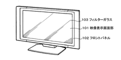
図8は、本発明が適用されるテレビを示す斜視図である。本適用例に係るテレビは、フロントパネル102やフィルターガラス103等から構成される映像表示画面部101を含み、その映像表示画面部101として本発明に係る表示装置を用いることにより作成される。 FIG. 8 is a perspective view showing a television to which the present invention is applied. The television according to this application example includes a video display screen unit 101 including a front panel 102, a filter glass 103, and the like, and is created by using the display device according to the present invention as the video display screen unit 101.
図9は、本発明が適用されるデジタルカメラを示す図であり、(A)は表側から見た斜視図、(B)は裏側から見た斜視図である。本適用例に係るデジタルカメラは、フラッシュ用の発光部111、表示部112、メニュースイッチ113、シャッターボタン114等を含み、その表示部112として本発明に係る表示装置を用いることにより作製される。 9A and 9B are diagrams showing a digital camera to which the present invention is applied. FIG. 9A is a perspective view seen from the front side, and FIG. 9B is a perspective view seen from the back side. The digital camera according to this application example includes a light emitting unit 111 for flash, a display unit 112, a menu switch 113, a shutter button 114, and the like, and is manufactured by using the display device according to the present invention as the display unit 112.
図10は、本発明が適用されるノート型パーソナルコンピュータを示す斜視図である。本適用例に係るノート型パーソナルコンピュータは、本体121に、文字等を入力するとき操作されるキーボード122、画像を表示する表示部123等を含み、その表示部123として本発明に係る表示装置を用いることにより作製される。 FIG. 10 is a perspective view showing a notebook personal computer to which the present invention is applied. A notebook personal computer according to this application example includes a main body 121 including a keyboard 122 that is operated when characters and the like are input, a display unit 123 that displays an image, and the like. It is produced by using.
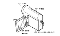
図11は、本発明が適用されるビデオカメラを示す斜視図である。本適用例に係るビデオカメラは、本体部131、前方を向いた側面に被写体撮影用のレンズ132、撮影時のスタート/ストップスイッチ133、表示部134等を含み、その表示部134として本発明に係る表示装置を用いることにより作製される。 FIG. 11 is a perspective view showing a video camera to which the present invention is applied. The video camera according to this application example includes a main body 131, a lens 132 for shooting an object on a side facing forward, a start / stop switch 133 at the time of shooting, a display unit 134, and the like. It is manufactured by using such a display device.
図12は、本発明が適用される携帯端末装置、例えば携帯電話機を示す図であり、(A)は開いた状態での正面図、(B)はその側面図、(C)は閉じた状態での正面図、(D)は左側面図、(E)は右側面図、(F)は上面図、(G)は下面図である。本適用例に係る携帯電話機は、上側筐体141、下側筐体142、連結部(ここではヒンジ部)143、ディスプレイ144、サブディスプレイ145、ピクチャーライト146、カメラ147等を含み、そのディスプレイ144やサブディスプレイ145として本発明に係る表示装置を用いることにより作製される。 12A and 12B are diagrams showing a mobile terminal device to which the present invention is applied, for example, a mobile phone. FIG. 12A is a front view in an opened state, FIG. 12B is a side view thereof, and FIG. (D) is a left side view, (E) is a right side view, (F) is a top view, and (G) is a bottom view. The mobile phone according to this application example includes an upper housing 141, a lower housing 142, a connecting portion (here, a hinge portion) 143, a display 144, a sub display 145, a picture light 146, a camera 147, and the like. And the sub display 145 is manufactured by using the display device according to the present invention.
次に、本発明の具体的な実施例、および実施例に対する比較例として、フルカラー表示装置を構成する各色発光の有機電界発光素子の製造手順を説明し、次にこれらの評価結果を説明する。 Next, as a specific example of the present invention and a comparative example to the example, a manufacturing procedure of organic electroluminescent elements for light emission of each color constituting the full-color display device will be described, and then the evaluation results will be described.
≪実施例≫
表示装置を構成する各色発光素子21r,21g,21bを、本発明に基づいて以下のように個別に作製した(図1〜図3参照)。
<Example>
Each color light emitting element 21r, 21g, 21b constituting the display device was individually manufactured as follows based on the present invention (see FIGS. 1 to 3).
<赤色発光素子21rの作製>
(工程S11)
支持基板31となるガラス基板の上に、厚さ200nmのモリブデンからなる光熱変換層33を通常のスパッタリング法により成膜した。次いで、光熱変換層33上に、窒化シリコンSiNXからなる酸化保護層34を100nmの膜厚でCVD法によって成膜した。
<Preparation of Red Light Emitting Element 21r>
(Process S11)
On the glass substrate used as the
次に、赤色転写層35rを塗布形成した。この際、α−NPDにBSNを30重量%の比率で混合したものをトルエン中に1重量%の濃度で溶解し、溶液とした。スピンコーターを使用し、前述の光熱変換層、酸化保護層を形成したガラス基板上に滴下し回転数1500rpmで回転させて塗膜(赤色転写層35r)を形成した。
Next, a
(工程S12)
塗布形成した赤色転写層35rを加熱処理した。赤色転写層35rを構成する主材料としてα−NPDが用いられており、そのガラス転移温度は96℃である。このため、加熱処理は、このガラス転移点より高く、融点以下の温度範囲で行われる。そこで窒素ガス中150℃において30分間加熱処理した。
(Process S12)
The
(工程S1)
装置基板1となるガラス基板の上に、銀合金層であるAPC(Ag-Pd-Cu)層(膜厚120nm)、ITOからなる透明導電層(膜厚10nm)をこの順に形成した2層構造の下部電極3を陽極としてパターン形成した。次に下部電極3の周縁を覆う状態で酸化シリコンの絶縁膜5をスパッタリング法により約2μmの厚さで成膜し、リソグラフィー法により下部電極3を露出させ、画素領域とした。その表面の上に、正孔注入層7として、m−MTDATAを10nmの膜厚で蒸着した。次に、正孔輸送層9として、α−NPDを35nmの膜厚で蒸着した。
(Process S1)
A two-layer structure in which an APC (Ag-Pd-Cu) layer (thickness 120 nm), which is a silver alloy layer, and a transparent conductive layer (thickness 10 nm) made of ITO are formed in this order on a glass substrate to be the device substrate 1 A pattern was formed using the
(工程S2)
成膜された有機層同士が向き合う状態で、上記工程S11,S12において作製した赤色転写基板30rを装置基板1の上に配置し、真空中で密着させた。両基板は、絶縁膜5の厚さによって、約2μmの小さな間隙が維持される。この状態で、装置基板1の画素領域に相等する領域に、転写用基板30rの裏側から波長800nmのレーザ光線を照射することにより、転写用基板30rから赤色転写層35rを熱転写させ、正孔輸送性の赤色発光層11rを形成した。レーザ光線のスポットサイズは、300μm×10μmとした。レーザ光線は、該光線の長手寸法に対して直交する方向において走査した。エネルギー密度は、1.8J/cm2とした。
(Process S2)
With the formed organic layers facing each other, the
(工程S4)
熱転写によって正孔輸送性の赤色発光層11rをパターン形成された装置基板1全体を30分間、加熱処理する工程を行った。この場合、正孔輸送層9のα−NPDのガラス転移温度が96℃であるため、100℃の設定温度を採用した。
(Process S4)
The
(工程S5)
加熱処理の後、電子輸送層13を成膜した。電子輸送層13として、8≡ヒドロキシキノリンアルミニウム(Alq3)を20nm程度の膜厚で蒸着成膜した。続いて、電子注入層17として、LiFを約0.3nm(蒸着速度〜0.01nm/sec)の膜厚で蒸着成膜した。次いで、上部電極19となる陰極としてMgAgを10nmの膜厚で蒸着成膜し、赤色発光素子21rを得た。
(Process S5)
After the heat treatment, an electron transport layer 13 was formed. As the electron transport layer 13, 8≡hydroxyquinoline aluminum (Alq 3) was deposited to a thickness of about 20 nm. Subsequently, LiF was deposited as an
<緑色発光素子21gの作製>
上記工程S11およびS12によって作製する転写用基板30gとして、正孔輸送性の赤色転写層35rを電子輸送性の緑色転写層35gに換えたものを用意した。
<Preparation of green light emitting element 21g>
As the
(工程S11)
緑色転写層35gの塗布形成においては、ADNからなるホスト材料に、クマリン6からなる緑色発光性のゲスト材料を5重量%の割合で混合したものをトルエンに対して0.8重量%の濃度で溶解した溶液を作製し、光熱変換層33および酸化保護層34が成膜された支持基板31上に、前記溶液を滴下しスピンコーターを使用して1500rpmの回転数で回転させて塗膜(緑色転写層35g)を形成した。
(Process S11)
In the coating formation of the
(工程S12)
塗布形成した緑色転写層35gを加熱処理した。緑色転写層35gを構成する主材料としてADNが用いられており、そのガラス転移温度は106℃である。この加熱処理は、このガラス転移点より高く、融点以下の温度範囲で行われる。そこで窒素ガス中160℃において30分間加熱処理した。
(Process S12)
The applied
以上のようにして作製した緑色転写基板30gを用い、工程S1〜工程S5を上記赤色発光素子の作製と同様に行い、緑色発光素子21gを得た。尚、工程S4の加熱処理においては、工程S12よりも低温の100℃での温度設定を採用した。
Using the
<青色発光素子21bの作製>
上記工程S11およびS12によって作製する転写用基板30bとして、正孔輸送性の赤色転写層35rを電子輸送性の青色転写層35bに換えたものを用意した。
<Preparation of Blue Light Emitting Element 21b>
As the
(工程S11)
青色転写層35bの塗布形成においては、ADNからなるホスト材料に、DPAVBiからなる青色発光性のゲスト材料を2.5重量%の割合で混合したものをトルエンに対して0.8重量%の濃度で溶解した溶液を作製し、光熱変換層33および酸化保護層34が成膜された支持基板31条に、前記溶液を滴下しスピンコーターを使用して1500rpmの回転数で回転させて塗膜(青色転写層35b)を形成した。
(Process S11)
In the coating formation of the
(工程S12)
塗布形成した緑色転写層35bを加熱処理した。青色発光層11bを構成する主材料としてADNが用いられており、そのガラス転移温度は106℃である。この加熱処理は、このガラス転移点より高く、融点以下の温度範囲で行われる。そこで窒素ガス中160℃において30分間加熱処理した。
(Process S12)
The
以上のようにして作製した青色転写基板30bを用い、工程S1〜工程S5を上記赤色発光素子の作製と同様に行い、青色発光素子21bを得た。尚、工程S4の加熱処理においては、工程S12よりも低温の100℃での温度設定を採用した。
Using the
≪比較例≫
表示装置を構成する各色発光素子を、上述した実施例における工程S12の加熱処理と、工程S4の加熱処理を省略して個別に作製した。
≪Comparative example≫
Each color light emitting element constituting the display device was individually manufactured by omitting the heat treatment in step S12 and the heat treatment in step S4 in the above-described embodiment.
≪評価結果≫
以上のようにして作製した実施例の各色発光素子および比較例の各色発光素子について、10mA/cm2の定電流密度を印加した状態で、分光放射輝度計を用いて色度(CIE-x,CIE-y)および発光効率を測定した。また、実施例と比較例で同色の発光素子が同輝度で発光するように電流印加を設定した状態で寿命試験を行い、100時間経過後の輝度減少率を測定した。これらの結果を下記表1に示す。
≪Evaluation results≫
The chromaticity (CIE-x, CIE) was measured using a spectral radiance meter in a state where a constant current density of 10 mA /

この表1から、赤色発光素子においては、比較例で作製した発光素子に対して、実施例で作製した発光素子は、発光効率が5.99[Cd/A]から7.7[Cd/A]と約30%の大幅な向上が確認されただけではなく、輝度減少率にみる発光寿命も28%から10%の大幅な向上が確認された。 According to Table 1, in the red light emitting element, the light emitting element manufactured in the example has a light emission efficiency of 5.99 [Cd / A] to 7.7 [Cd / A] as compared with the light emitting element manufactured in the comparative example. ], A significant improvement of about 30% was confirmed, and the light emission lifetime in terms of the luminance reduction rate was also confirmed to be a significant improvement of 28% to 10%.
また、緑色発光素子および青色発光素子においても、比較例で作製した発光素子に対して、実施例で作製した発光素子での発光効率の向上が確認され、輝度減少率にみる発光寿命も大幅に向上することが確認された。 In addition, in the green light emitting element and the blue light emitting element, it was confirmed that the luminous efficiency of the light emitting element manufactured in the example was improved with respect to the light emitting element manufactured in the comparative example, and the light emission lifetime in terms of the luminance reduction rate was greatly increased. It was confirmed to improve.
以上の結果から本発明の方法を適用して表示装置を作製することにより、転写用基板の作製において転写層を塗布成膜した場合であっても、赤色発光素子、緑色発光素子、および青色発光素子の全てにおいて、輝度半減寿命を高く維持した状態で発光効率の向上を図り、フルカラーの表示装置における表示性能を向上させることが可能であることが確認された。 From the above results, a display device is manufactured by applying the method of the present invention, so that a red light emitting element, a green light emitting element, and a blue light emitting element can be formed even when a transfer layer is applied and formed in the manufacture of a transfer substrate. It was confirmed that in all the elements, it was possible to improve the light emission efficiency while maintaining a high luminance half-life, and to improve the display performance in a full-color display device.
1…装置基板、3…下部電極(陽極)、11r…赤色発光層、11g…緑色発光層、11b…青色発光層、19…上部電極(陰極)、21r…赤色発光素子、21g…緑色発光素子、21b…青色発光素子、23…表示装置、31…支持基板、33…熱変換層、35r…赤色転写層、35g…緑色転写層、35b…青色転写層
DESCRIPTION OF
Claims (12)
前記支持基板上において前記転写層を加熱処理する工程と、
前記加熱処理された転写層を装置基板上に熱転写する工程とを行う
ことを特徴とする表示装置の製造方法。 Coating and forming a transfer layer containing an organic light emitting material on a support substrate;
Heat-treating the transfer layer on the support substrate;
And a step of thermally transferring the heat-treated transfer layer onto an apparatus substrate.
前記加熱処理は、前記転写層を構成する有機材料のガラス転移点以上でかつ融点より低い温度で行われる
ことを特徴とする表示装置の製造方法。 In the manufacturing method of the display device according to claim 1,
The method for manufacturing a display device, wherein the heat treatment is performed at a temperature higher than or equal to a glass transition point of an organic material constituting the transfer layer and lower than a melting point.
前記加熱工程は、不活性な雰囲気中で行われる
ことを特徴とする表示装置の製造方法。 In the manufacturing method of the display device according to claim 1,
The method for manufacturing a display device, wherein the heating step is performed in an inert atmosphere.
前記装置基板上に熱転写された転写層を加熱処理する工程を行う
ことを特徴とする表示装置の製造方法。 In the manufacturing method of the display device according to claim 1,
A method of manufacturing a display device, comprising: performing a heat treatment on a transfer layer thermally transferred onto the device substrate.
前記装置基板上に熱転写された転写層の加熱処理は、当該転写層を構成する有機光材料のガラス転移点以上でかつ融点より低い温度で行われる
ことを特徴とする表示装置の製造方法。 In the manufacturing method of the display device according to claim 4,
The method for manufacturing a display device, wherein the heat treatment of the transfer layer thermally transferred onto the device substrate is performed at a temperature not lower than the glass transition point of the organic optical material constituting the transfer layer and lower than the melting point.
前記装置基板上に熱転写された転写層の加熱処理は、前記支持基板上において行われる前記転写層の加熱処理よりも低い温度で行われる
ことを特徴とする表示装置の製造方法。 In the manufacturing method of the display device according to claim 5,
The method for manufacturing a display device, wherein the heat treatment of the transfer layer thermally transferred onto the device substrate is performed at a lower temperature than the heat treatment of the transfer layer performed on the support substrate.
前記転写層を装置基板上に熱転写する工程では、前記装置基板上に形成された下部電極上に前記転写層を熱転写し、
前記転写層が熱転写された前記装置基板上に、当該転写層に積層させる状態で上部電極を形成する工程を行う
ことを特徴とする表示装置の製造方法。 In the manufacturing method of the display device according to claim 1,
In the step of thermally transferring the transfer layer onto the device substrate, the transfer layer is thermally transferred onto a lower electrode formed on the device substrate,
A method of manufacturing a display device, comprising: forming an upper electrode on the device substrate onto which the transfer layer has been thermally transferred, in a state of being laminated on the transfer layer.
前記上部電極を形成した後に、前記下部電極から当該上部電極までを積層してなる発光素子を覆う状態で保護膜を形成する工程を行うと共に、
前記転写層を加熱転写する工程から前記保護膜を形成する工程までを一連の不活性な雰囲気中で行う
を特徴とする表示装置の製造方法。 In the manufacturing method of the display device according to claim 7,
After forming the upper electrode, performing a step of forming a protective film in a state of covering the light emitting element formed by laminating the lower electrode to the upper electrode,
A method for manufacturing a display device, wherein the process from the step of transferring the transfer layer to the step of forming the protective film is performed in a series of inert atmospheres.
前記支持基板上に前記転写層を塗布形成する工程では、当該支持基板上の全面に当該転写層を形成し、
前記転写層を装置基板上に熱転写する工程では、当該転写層の一部を当該装置基板上にパターン転写する
ことを特徴とする表示装置の製造方法。 In the manufacturing method of the display device according to claim 1,
In the step of applying and forming the transfer layer on the support substrate, the transfer layer is formed on the entire surface of the support substrate,
In the process of thermally transferring the transfer layer onto the device substrate, a part of the transfer layer is pattern transferred onto the device substrate.
前記転写層を塗布形成する工程では、前記支持基板上に当該転写層をパターン形成し、
前記転写層を装置基板上に熱転写する工程では、パターン形成された当該転写層を当該装置基板上に一括転写する
ことを特徴とする表示装置の製造方法。 In the manufacturing method of the display device according to claim 1,
In the step of coating and forming the transfer layer, the transfer layer is patterned on the support substrate,
In the step of thermally transferring the transfer layer onto the device substrate, the pattern-formed transfer layer is collectively transferred onto the device substrate.
前記転写層を塗布形成する工程では、前記支持基板上に異なる種類の有機発光材料を含有する各転写層を個別にパターン形成する
ことを特徴とする表示装置の製造方法。 In the manufacturing method of the display device according to claim 10,
In the step of applying and forming the transfer layer, each transfer layer containing different kinds of organic light-emitting materials is individually patterned on the support substrate.
前記転写層を塗布形成する工程では、前記支持基板上にパターン形成された熱変換層を覆う状態で、当該支持基板上の全面に当該転写層を形成し、
前記転写層を装置基板上に熱転写する工程では、パターン形成された前記熱変換層上における当該転写層部分のみを当該装置基板上に一括転写する
ことを特徴とする表示装置の製造方法。 In the manufacturing method of the display device according to claim 1,
In the step of coating and forming the transfer layer, the transfer layer is formed on the entire surface of the support substrate in a state of covering the heat conversion layer patterned on the support substrate,
In the step of thermally transferring the transfer layer onto the device substrate, only the transfer layer portion on the patterned heat conversion layer is collectively transferred onto the device substrate.
Priority Applications (5)
| Application Number | Priority Date | Filing Date | Title |
|---|---|---|---|
| JP2007072965A JP2008235010A (en) | 2007-03-20 | 2007-03-20 | Method of manufacturing display device |
| TW97107223A TW200904240A (en) | 2007-03-20 | 2008-02-29 | Method for manufacturing display device |
| KR20080023271A KR20080085705A (en) | 2007-03-20 | 2008-03-13 | Method for manufacturing display device |
| CN2008100875012A CN101272643B (en) | 2007-03-20 | 2008-03-19 | Method for manufacturing display device |
| US12/051,603 US20080233827A1 (en) | 2007-03-20 | 2008-03-19 | Method for manufacturing display device |
Applications Claiming Priority (1)
| Application Number | Priority Date | Filing Date | Title |
|---|---|---|---|
| JP2007072965A JP2008235010A (en) | 2007-03-20 | 2007-03-20 | Method of manufacturing display device |
Publications (2)
| Publication Number | Publication Date |
|---|---|
| JP2008235010A true JP2008235010A (en) | 2008-10-02 |
| JP2008235010A5 JP2008235010A5 (en) | 2008-11-13 |
Family
ID=39775224
Family Applications (1)
| Application Number | Title | Priority Date | Filing Date |
|---|---|---|---|
| JP2007072965A Pending JP2008235010A (en) | 2007-03-20 | 2007-03-20 | Method of manufacturing display device |
Country Status (5)
| Country | Link |
|---|---|
| US (1) | US20080233827A1 (en) |
| JP (1) | JP2008235010A (en) |
| KR (1) | KR20080085705A (en) |
| CN (1) | CN101272643B (en) |
| TW (1) | TW200904240A (en) |
Cited By (4)
| Publication number | Priority date | Publication date | Assignee | Title |
|---|---|---|---|---|
| WO2011114873A1 (en) * | 2010-03-18 | 2011-09-22 | 株式会社半導体エネルギー研究所 | Film-forming method and film-forming substrate production method |
| JP2011195870A (en) * | 2010-03-18 | 2011-10-06 | Semiconductor Energy Lab Co Ltd | Film forming method |
| US8900675B2 (en) | 2010-03-18 | 2014-12-02 | Semiconductor Energy Laboratory Co., Ltd. | Deposition method and method for manufacturing deposition substrate |
| US8951816B2 (en) | 2010-03-18 | 2015-02-10 | Semiconductor Energy Laboratory Co., Ltd. | Film forming method |
Families Citing this family (8)
| Publication number | Priority date | Publication date | Assignee | Title |
|---|---|---|---|---|
| WO2012091243A1 (en) * | 2010-12-27 | 2012-07-05 | 제일모직 주식회사 | Thermal transfer film |
| JP5695535B2 (en) | 2011-09-27 | 2015-04-08 | 株式会社東芝 | Manufacturing method of display device |
| TW201321871A (en) * | 2011-11-29 | 2013-06-01 | Au Optronics Corp | Display panel and manufacturing method thereof |
| KR20150012530A (en) * | 2013-07-25 | 2015-02-04 | 삼성디스플레이 주식회사 | Donor substrate for trnasfer and manufacturing method of organic light emitting diode display |
| JP6392874B2 (en) * | 2013-12-26 | 2018-09-19 | カティーバ, インコーポレイテッド | Apparatus and techniques for heat treatment of electronic devices |
| KR102303994B1 (en) * | 2014-10-20 | 2021-09-23 | 삼성디스플레이 주식회사 | Method for manufacturing substrate for organic light emitting diode |
| CN107221548A (en) * | 2016-03-22 | 2017-09-29 | 上海和辉光电有限公司 | OLED display panel, intelligent display glass device and preparation method |
| US10615345B2 (en) * | 2016-06-03 | 2020-04-07 | The Trustees Of Princeton University | Method and device for using an organic underlayer to enable crystallization of disordered organic thin films |
Citations (11)
| Publication number | Priority date | Publication date | Assignee | Title |
|---|---|---|---|---|
| JP2002216957A (en) * | 2001-01-19 | 2002-08-02 | Sharp Corp | Manufacturing method of organic led display panel by using transcription method and organic led display panel manufactured by it |
| JP2003077657A (en) * | 2001-09-05 | 2003-03-14 | Sharp Corp | Coating liquid for forming organic led layer, donor film for organic led, manufacturing method for organic led display panel using the same, and organic led display panel |
| JP2003187972A (en) * | 2001-12-20 | 2003-07-04 | Dainippon Printing Co Ltd | Manufacturing method of organic el element and organic el transferring body and transferred body |
| JP2003347054A (en) * | 2002-05-29 | 2003-12-05 | Sharp Corp | Film for thin film transfer, its manufacturing method, and organic el element using same |
| JP2004193018A (en) * | 2002-12-12 | 2004-07-08 | Fuji Photo Film Co Ltd | Manufacturing method of organic electroluminescent element and organic electroluminescent element |
| JP2005116238A (en) * | 2003-10-03 | 2005-04-28 | Tdk Corp | Organic el element and organic el display |
| WO2005059951A2 (en) * | 2003-12-19 | 2005-06-30 | Cambridge Display Technology Limited | Optical device comprising a charge transport layer of insoluble organic material and method for the production thereof |
| JP2006086069A (en) * | 2004-09-17 | 2006-03-30 | Three M Innovative Properties Co | Organic electroluminescent element and its manufacturing method |
| JP2006108098A (en) * | 2004-10-05 | 2006-04-20 | Samsung Sdi Co Ltd | Manufacturing method for donor substrate and manufacturing method for organic electroluminescence display device using donor substrate |
| JP2006123546A (en) * | 2004-10-19 | 2006-05-18 | Samsung Sdi Co Ltd | Manufacturing method of donor substrate and organic electroluminescence display apparatus |
| JP2006231407A (en) * | 2005-02-22 | 2006-09-07 | Samsung Sdi Co Ltd | Laser irradiation device and laser induced thermal imaging method |
Family Cites Families (8)
| Publication number | Priority date | Publication date | Assignee | Title |
|---|---|---|---|---|
| US7005166B2 (en) * | 2001-06-19 | 2006-02-28 | Dai Nippon Printing Co., Ltd. | Method for fluorescent image formation, print produced thereby and thermal transfer sheet thereof |
| US6699597B2 (en) * | 2001-08-16 | 2004-03-02 | 3M Innovative Properties Company | Method and materials for patterning of an amorphous, non-polymeric, organic matrix with electrically active material disposed therein |
| KR100490539B1 (en) * | 2002-09-19 | 2005-05-17 | 삼성에스디아이 주식회사 | Organic electroluminescence device and manufacturing method thereof |
| US7052355B2 (en) * | 2003-10-30 | 2006-05-30 | General Electric Company | Organic electro-optic device and method for making the same |
| US20050123850A1 (en) * | 2003-12-09 | 2005-06-09 | 3M Innovative Properties Company | Thermal transfer of light-emitting dendrimers |
| KR100731728B1 (en) * | 2004-08-27 | 2007-06-22 | 삼성에스디아이 주식회사 | Donor substrate for laser induced thermal imaging method and method for fabricating organic electro-luminescence display device by the same |
| KR20060020030A (en) * | 2004-08-30 | 2006-03-06 | 삼성에스디아이 주식회사 | Fabricating method of donor device |
| KR100611767B1 (en) * | 2004-08-30 | 2006-08-10 | 삼성에스디아이 주식회사 | donor substrate for laser induced thermal imaging and method of fabricating electroluminescence display device using the same substrate |
-
2007
- 2007-03-20 JP JP2007072965A patent/JP2008235010A/en active Pending
-
2008
- 2008-02-29 TW TW97107223A patent/TW200904240A/en unknown
- 2008-03-13 KR KR20080023271A patent/KR20080085705A/en not_active Application Discontinuation
- 2008-03-19 CN CN2008100875012A patent/CN101272643B/en not_active Expired - Fee Related
- 2008-03-19 US US12/051,603 patent/US20080233827A1/en not_active Abandoned
Patent Citations (12)
| Publication number | Priority date | Publication date | Assignee | Title |
|---|---|---|---|---|
| JP2002216957A (en) * | 2001-01-19 | 2002-08-02 | Sharp Corp | Manufacturing method of organic led display panel by using transcription method and organic led display panel manufactured by it |
| JP2003077657A (en) * | 2001-09-05 | 2003-03-14 | Sharp Corp | Coating liquid for forming organic led layer, donor film for organic led, manufacturing method for organic led display panel using the same, and organic led display panel |
| JP2003187972A (en) * | 2001-12-20 | 2003-07-04 | Dainippon Printing Co Ltd | Manufacturing method of organic el element and organic el transferring body and transferred body |
| JP2003347054A (en) * | 2002-05-29 | 2003-12-05 | Sharp Corp | Film for thin film transfer, its manufacturing method, and organic el element using same |
| JP2004193018A (en) * | 2002-12-12 | 2004-07-08 | Fuji Photo Film Co Ltd | Manufacturing method of organic electroluminescent element and organic electroluminescent element |
| JP2005116238A (en) * | 2003-10-03 | 2005-04-28 | Tdk Corp | Organic el element and organic el display |
| WO2005059951A2 (en) * | 2003-12-19 | 2005-06-30 | Cambridge Display Technology Limited | Optical device comprising a charge transport layer of insoluble organic material and method for the production thereof |
| JP2007520858A (en) * | 2003-12-19 | 2007-07-26 | ケンブリッジ ディスプレイ テクノロジー リミテッド | Optical device |
| JP2006086069A (en) * | 2004-09-17 | 2006-03-30 | Three M Innovative Properties Co | Organic electroluminescent element and its manufacturing method |
| JP2006108098A (en) * | 2004-10-05 | 2006-04-20 | Samsung Sdi Co Ltd | Manufacturing method for donor substrate and manufacturing method for organic electroluminescence display device using donor substrate |
| JP2006123546A (en) * | 2004-10-19 | 2006-05-18 | Samsung Sdi Co Ltd | Manufacturing method of donor substrate and organic electroluminescence display apparatus |
| JP2006231407A (en) * | 2005-02-22 | 2006-09-07 | Samsung Sdi Co Ltd | Laser irradiation device and laser induced thermal imaging method |
Cited By (6)
| Publication number | Priority date | Publication date | Assignee | Title |
|---|---|---|---|---|
| WO2011114873A1 (en) * | 2010-03-18 | 2011-09-22 | 株式会社半導体エネルギー研究所 | Film-forming method and film-forming substrate production method |
| JP2011195870A (en) * | 2010-03-18 | 2011-10-06 | Semiconductor Energy Lab Co Ltd | Film forming method |
| US8815352B2 (en) | 2010-03-18 | 2014-08-26 | Semiconductor Energy Laboratory Co., Ltd. | Film forming method and method for manufacturing film-formation substrate |
| US8900675B2 (en) | 2010-03-18 | 2014-12-02 | Semiconductor Energy Laboratory Co., Ltd. | Deposition method and method for manufacturing deposition substrate |
| US8951816B2 (en) | 2010-03-18 | 2015-02-10 | Semiconductor Energy Laboratory Co., Ltd. | Film forming method |
| JP5666556B2 (en) * | 2010-03-18 | 2015-02-12 | 株式会社半導体エネルギー研究所 | Film forming method and film forming substrate manufacturing method |
Also Published As
| Publication number | Publication date |
|---|---|
| KR20080085705A (en) | 2008-09-24 |
| CN101272643B (en) | 2010-10-13 |
| CN101272643A (en) | 2008-09-24 |
| US20080233827A1 (en) | 2008-09-25 |
| TW200904240A (en) | 2009-01-16 |
Similar Documents
| Publication | Publication Date | Title |
|---|---|---|
| JP2008235010A (en) | Method of manufacturing display device | |
| KR101202515B1 (en) | Methods of making displays | |
| US9209233B2 (en) | Method for manufacturing display and display | |
| US7691783B2 (en) | Transfer substrate, method for fabricating display device, and display device | |
| JP4793071B2 (en) | Display device and manufacturing method of display device | |
| JP2007173145A (en) | Substrate for transfer, transfer method and manufacturing method for organic electroluminescent element | |
| JP4957929B2 (en) | Method for manufacturing donor substrate and display device | |
| KR101361017B1 (en) | Method for manufacturing a display device | |
| US20100159165A1 (en) | Transfer substrate and method of manufacturing a display apparatus | |
| KR20060109840A (en) | Display device and a method of manufacturing the same | |
| JP2010034022A (en) | Donor substrate, and manufacturing method of display | |
| US20090038550A1 (en) | Evaporation source, manufacturing method of the same and manufacturing method of an organic el display device | |
| JP4396864B2 (en) | Display device and manufacturing method thereof | |
| US7993806B2 (en) | Transfer substrate, and fabrication process of organic electroluminescent devices | |
| JP2013137931A (en) | Light-emitting element, method of manufacturing the same, display device, and electronic apparatus | |
| JP2009146715A (en) | Donor substrate, and manufacturing method for display device | |
| TW201349618A (en) | Organic electroluminescence unit, method of manufacturing organic electroluminescence unit, and electronic apparatus | |
| JP2009146716A (en) | Display device and donor substrate | |
| JP2008311103A (en) | Manufacturing method of display device, and the display device | |
| JP2009266451A (en) | Method for manufacturing display, and transfer substrate | |
| JP2008235011A (en) | Method of manufacturing display method | |
| JP2006309955A (en) | Manufacturing method for organic electroluminescent element, and organic electroluminescent element | |
| JP2010192826A (en) | Donor substrate and method of manufacturing display device | |
| JP2011034852A (en) | Method of manufacturing donor substrate, donor substrate, and method of manufacturing display device | |
| JP2011108421A (en) | Manufacturing method of display device |
Legal Events
| Date | Code | Title | Description |
|---|---|---|---|
| A521 | Request for written amendment filed |
Free format text: JAPANESE INTERMEDIATE CODE: A523 Effective date: 20080916 |
|
| A621 | Written request for application examination |
Free format text: JAPANESE INTERMEDIATE CODE: A621 Effective date: 20080916 |
|
| A977 | Report on retrieval |
Free format text: JAPANESE INTERMEDIATE CODE: A971007 Effective date: 20090806 |
|
| A131 | Notification of reasons for refusal |
Free format text: JAPANESE INTERMEDIATE CODE: A131 Effective date: 20090811 |
|
| A521 | Request for written amendment filed |
Free format text: JAPANESE INTERMEDIATE CODE: A523 Effective date: 20090917 |
|
| A131 | Notification of reasons for refusal |
Free format text: JAPANESE INTERMEDIATE CODE: A131 Effective date: 20091020 |
|
| RD02 | Notification of acceptance of power of attorney |
Free format text: JAPANESE INTERMEDIATE CODE: A7422 Effective date: 20091021 |
|
| A521 | Request for written amendment filed |
Free format text: JAPANESE INTERMEDIATE CODE: A821 Effective date: 20091026 |
|
| RD04 | Notification of resignation of power of attorney |
Free format text: JAPANESE INTERMEDIATE CODE: A7424 Effective date: 20091109 |
|
| A521 | Request for written amendment filed |
Free format text: JAPANESE INTERMEDIATE CODE: A523 Effective date: 20091214 |
|
| A02 | Decision of refusal |
Free format text: JAPANESE INTERMEDIATE CODE: A02 Effective date: 20101019 |